
Integrated Microprocessor User’s Manual - Digi-Key Sheets/Motorola PDFs/MCF5206... · NEW JERSEY,...
449
MOTOROLA, 1997 All Rights Reserved. μ Motorola reserves the right to make changes without further notice to any products herein. Motorola makes no warranty, representation or guarantee regarding the suitability of its products for any particular purpose, nor does Motorola assume any liability arising out of the application or use of any product or circuit, and specifically disclaims any and all liability, including without limitation consequential or incidental damages. "Typical" parameters can and do vary in different applications. All operating parameters, including "Typicals" must be validated for each customer application by customer's technical experts. Motorola does not convey any license under its patent rights nor the rights of others. Motorola products are not designed, intended, or authorized for use as components in systems intended for surgical implant into the body, or other applications intended to support or sustain life, or for any other application in which the failure of the Motorola product could create a situation where personal injury or death may occur. Should Buyer purchase or use Motorola products for any such unintended or unauthorized application, Buyer shall indemnify and hold Motorola and its officers, employees, subsidiaries, affiliates, and distributors harmless against all claims, costs, damages, and expenses, and reasonable attorney fees arising out of, directly or indirectly, any claim of personal injury or death associated with such unintended or unauthorized use, even if such claim alleges that Motorola was negligent regarding the design or manufacture of the part. Motorola and are registered trademarks of Motorola, Inc. Motorola, Inc. is an Equal Opportunity/Affirmative Action Employer. MCF5206 ColdFire Integrated Microprocessor User’s Manual TM
Transcript of Integrated Microprocessor User’s Manual - Digi-Key Sheets/Motorola PDFs/MCF5206... · NEW JERSEY,...

MOTOROLA, 1997 All Rights Reserved.
µ
Motorola reserves the right to make changes without further notice to any products herein. Motorola makes no warranty, representation or guarantee regarding the suitability of its products for any particular purpose, nor does Motorola assume any liability arising out of the application or use of any product or circuit, and specifically disclaims any and all liability, including without limitation consequential or incidental damages. "Typical" parameters can and do vary in different applications. All operating parameters, including "Typicals" must be validated for each customer application by customer's technical experts. Motorola does not convey any license under its patent rights nor the rights of others. Motorola products are not designed, intended, or authorized for use as components in systems intended for surgical implant into the body, or other applications intended to support or sustain life, or for any other application in which the failure of the Motorola product could create a situation where personal injury or death may occur. Should Buyer purchase or use Motorola products for any such unintended or unauthorized application, Buyer shall indemnify and hold Motorola and its officers, employees, subsidiaries, affiliates, and distributors harmless against all claims, costs, damages, and expenses, and reasonable attorney fees arising out of, directly or indirectly, any claim of personal injury or death associated with such unintended or unauthorized use, even if such claim alleges that Motorola was negligent regarding the design or manufacture of the part. Motorola and are registered trademarks of Motorola, Inc. Motorola, Inc. is an Equal Opportunity/Affirmative Action Employer.
MCF5206
ColdFire
Integrated Microprocessor
User’s Manual
TM


MOTOROLA
MCF5206 USER’S MANUAL
iii
DOCUMENTATION FEEDBACK
FAX 512-891-8593—Documentation Comments Only (no technical questions please)http: / / www.mot.com/hpesd/docs_survey.html—Documentation Feedback Only
The Technical Communications Department welcomes your suggestions for improving ourdocumentation and encourages you to complete the documentation feedback form at theWorld Wide Web address listed above. In return for your efforts, you will receive a smalltoken of our appreciation. Your help helps us measure how well we are serving your infor-mation requirements.
The Technical Communications Department also provides a fax number for you to submitany questions or comments about this document or how to order other documents. Pleaseprovide the part number and revision number (located in upper right-hand corner of thecover) and the title of the document. When referring to items in the manual, please referenceby the page number, paragraph number, figure number, table number, and line number ifneeded. Please do not fax technical questions to this number.
When sending a fax, please provide your name, company, fax number, and phone numberincluding area code.
For Internet Access:
Web Only: http: // www.mot.com/aesop
For Hotline Questions:
FAX (US or Canada): 1-800-248-8567
iv
MCF5206 USER’S MANUAL
MOTOROLA
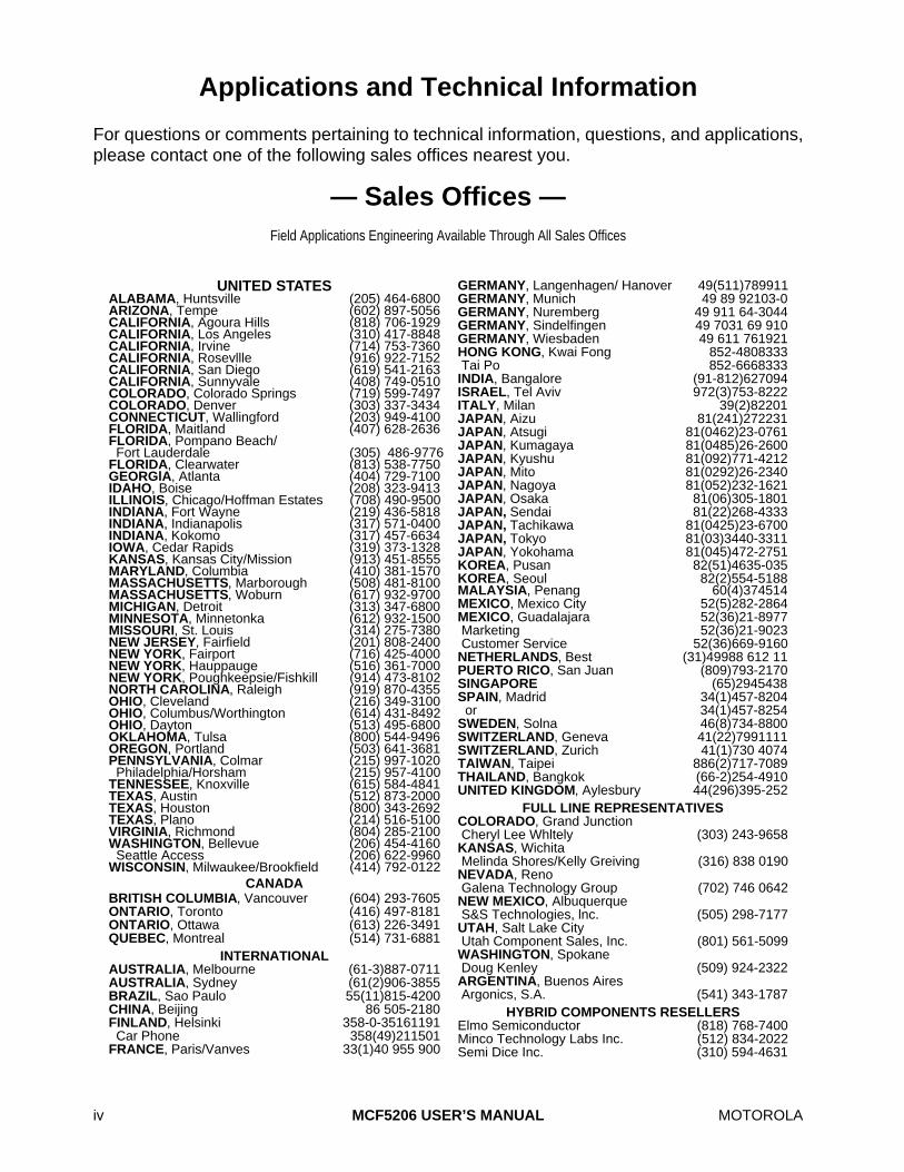
Applications and Technical Information
For questions or comments pertaining to technical information, questions, and applications,please contact one of the following sales offices nearest you.
— Sales Offices —
Field Applications Engineering Available Through All Sales Offices
UNITED STATES
ALABAMA
, Huntsville (205) 464-6800
ARIZONA
, Tempe (602) 897-5056
CALIFORNIA
, Agoura Hills (818) 706-1929
CALIFORNIA
, Los Angeles (310) 417-8848
CALIFORNIA
, Irvine (714) 753-7360
CALIFORNIA
, Rosevllle (916) 922-7152
CALIFORNIA
, San Diego (619) 541-2163
CALIFORNIA
, Sunnyvale (408) 749-0510
COLORADO
, Colorado Springs (719) 599-7497
COLORADO
, Denver (303) 337-3434
CONNECTICUT
, Wallingford (203) 949-4100
FLORIDA
, Maitland (407) 628-2636
FLORIDA
, Pompano Beach/ Fort Lauderdale (305) 486-9776
FLORIDA
, Clearwater (813) 538-7750
GEORGlA
, Atlanta (404) 729-7100
IDAHO
, Boise (208) 323-9413
ILLINOIS
, Chicago/Hoffman Estates (708) 490-9500
INDlANA
, Fort Wayne (219) 436-5818
INDIANA
, Indianapolis (317) 571-0400
INDIANA
, Kokomo (317) 457-6634
IOWA
, Cedar Rapids (319) 373-1328
KANSAS
, Kansas City/Mission (913) 451-8555
MARYLAND
, Columbia (410) 381-1570
MASSACHUSETTS
, Marborough (508) 481-8100
MASSACHUSETTS
, Woburn (617) 932-9700
MICHIGAN
, Detroit (313) 347-6800
MINNESOTA
, Minnetonka (612) 932-1500
MISSOURI
, St. Louis (314) 275-7380
NEW JERSEY
, Fairfield (201) 808-2400
NEW YORK
, Fairport (716) 425-4000
NEW YORK
, Hauppauge (516) 361-7000
NEW YORK
, Poughkeepsie/Fishkill (914) 473-8102
NORTH CAROLINA
, Raleigh (919) 870-4355
OHIO
, Cleveland (216) 349-3100
OHIO
, Columbus/Worthington (614) 431-8492
OHIO
, Dayton (513) 495-6800
OKLAHOMA
, Tulsa (800) 544-9496
OREGON
, Portland (503) 641-3681
PENNSYLVANIA
, Colmar (215) 997-1020 Philadelphia/Horsham (215) 957-4100
TENNESSEE
, Knoxville (615) 584-4841
TEXAS
, Austin (512) 873-2000
TEXAS
, Houston (800) 343-2692
TEXAS
, Plano (214) 516-5100
VIRGINIA
, Richmond (804) 285-2100
WASHINGTON
, Bellevue (206) 454-4160 Seattle Access (206) 622-9960
WISCONSIN
, Milwaukee/Brookfield (414) 792-0122
CANADABRITISH COLUMBIA
, Vancouver (604) 293-7605
ONTARIO
, Toronto (416) 497-8181
ONTARIO
, Ottawa (613) 226-3491
QUEBEC
, Montreal (514) 731-6881
INTERNATIONALAUSTRALIA
, Melbourne (61-3)887-0711
AUSTRALIA
, Sydney (61(2)906-3855
BRAZIL
, Sao Paulo 55(11)815-4200
CHINA
, Beijing 86 505-2180
FINLAND
, Helsinki 358-0-35161191 Car Phone 358(49)211501
FRANCE
, Paris/Vanves 33(1)40 955 900
GERMANY
, Langenhagen/ Hanover 49(511)789911
GERMANY
, Munich 49 89 92103-0
GERMANY
, Nuremberg 49 911 64-3044
GERMANY
, Sindelfingen 49 7031 69 910
GERMANY
, Wiesbaden 49 611 761921
HONG KONG
, Kwai Fong 852-4808333 Tai Po 852-6668333
INDIA
, Bangalore (91-812)627094
ISRAEL
, Tel Aviv 972(3)753-8222
ITALY
, Milan 39(2)82201
JAPAN
, Aizu 81(241)272231
JAPAN
, Atsugi 81(0462)23-0761
JAPAN
, Kumagaya 81(0485)26-2600
JAPAN
, Kyushu 81(092)771-4212
JAPAN
, Mito 81(0292)26-2340
JAPAN
, Nagoya 81(052)232-1621
JAPAN
, Osaka 81(06)305-1801
JAPAN,
Sendai 81(22)268-4333
JAPAN,
Tachikawa 81(0425)23-6700
JAPAN,
Tokyo 81(03)3440-3311
JAPAN
, Yokohama 81(045)472-2751
KOREA
, Pusan 82(51)4635-035
KOREA
, Seoul 82(2)554-5188
MALAYSIA
, Penang 60(4)374514
MEXICO
, Mexico City 52(5)282-2864
MEXICO
, Guadalajara 52(36)21-8977 Marketing 52(36)21-9023 Customer Service 52(36)669-9160
NETHERLANDS
, Best (31)49988 612 11
PUERTO RICO
, San Juan (809)793-2170
SINGAPORE
(65)2945438
SPAIN
, Madrid 34(1)457-8204 or 34(1)457-8254
SWEDEN
, Solna 46(8)734-8800
SWITZERLAND
, Geneva 41(22)7991111
SWITZERLAND
, Zurich 41(1)730 4074
TAlWAN
, Taipei 886(2)717-7089
THAILAND
, Bangkok (66-2)254-4910
UNITED KINGDOM
, Aylesbury 44(296)395-252
FULL LINE REPRESENTATIVESCOLORADO
, Grand Junction Cheryl Lee Whltely (303) 243-9658
KANSAS
, Wichita Melinda Shores/Kelly Greiving (316) 838 0190
NEVADA
, Reno Galena Technology Group (702) 746 0642
NEW MEXICO
, Albuquerque S&S Technologies, lnc. (505) 298-7177
UTAH
, Salt Lake City Utah Component Sales, Inc. (801) 561-5099
WASHINGTON
, Spokane Doug Kenley (509) 924-2322
ARGENTINA
, Buenos Aires Argonics, S.A. (541) 343-1787
HYBRID COMPONENTS RESELLERS
Elmo Semiconductor (818) 768-7400Minco Technology Labs Inc. (512) 834-2022Semi Dice Inc. (310) 594-4631

MOTOROLA
MCF5206 USER’S MANUAL
v
PREFACE
The
MCF5206 ColdFire Integrated Microprocessor User’s Manual
describes theprogramming, capabilities, and operation of the MCF5206 device. Refer to the
MCF5200ColdFire Family Programmer’s Reference Manual
for information on the ColdFire Family ofmicroprocessors.
TRADEMARKS
All trademarks reside with their respective owners.
CONTENTS
This user manual is organized as follows:
Section 1: IntroductionSection 2: Signal DescriptionSection 3: ColdFire CoreSection 4: Instruction CacheSection 5: SRAMSection 6: Bus OperationSection 7: System Integration Module (SIM)Section 8: Chip-Select ModuleSection 9: Parallel Port (General-Purpose I/O) ModuleSection 10: DRAM ControllerSection 11: UART ModuleSection 12: M-Bus ModuleSection 13: Timer ModuleSection 14: Debug SupportSection 15: IEEE 1149.1 Test Access Port (JTAG)Section 16: Electrical CharacteristicsSection 17: Mechanical CharacteristicsAppendix A: Memory MapAppendix B: Porting from M68K ArchitecturesIndex
MOTOROLA
MCF5206 USERÕS MANUAL Rev 1.0
i
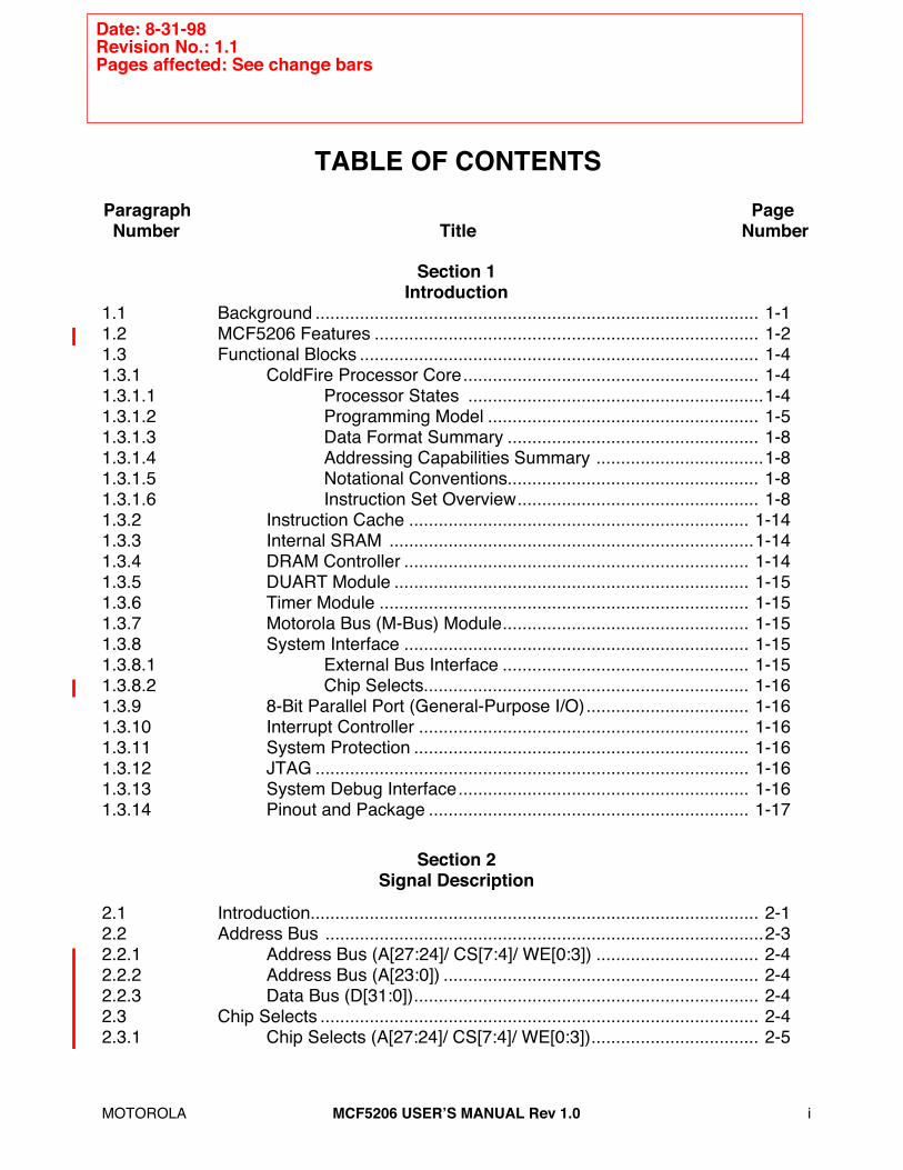
TABLE OF CONTENTS
Paragraph PageNumber Title Number
Section 1Introduction
1.1 Background .......................................................................................... 1-11.2 MCF5206 Features .............................................................................. 1-21.3 Functional Blocks ................................................................................. 1-41.3.1 ColdFire Processor Core............................................................ 1-41.3.1.1 Processor States ............................................................1-41.3.1.2 Programming Model ....................................................... 1-51.3.1.3 Data Format Summary ................................................... 1-81.3.1.4 Addressing Capabilities Summary ..................................1-81.3.1.5 Notational Conventions................................................... 1-81.3.1.6 Instruction Set Overview................................................. 1-81.3.2 Instruction Cache ..................................................................... 1-141.3.3 Internal SRAM ..........................................................................1-141.3.4 DRAM Controller ...................................................................... 1-141.3.5 DUART Module ........................................................................ 1-151.3.6 Timer Module ........................................................................... 1-151.3.7 Motorola Bus (M-Bus) Module.................................................. 1-151.3.8 System Interface ...................................................................... 1-151.3.8.1 External Bus Interface .................................................. 1-151.3.8.2 Chip Selects.................................................................. 1-161.3.9 8-Bit Parallel Port (General-Purpose I/O)................................. 1-161.3.10 Interrupt Controller ................................................................... 1-161.3.11 System Protection .................................................................... 1-161.3.12 JTAG ........................................................................................ 1-161.3.13 System Debug Interface........................................................... 1-161.3.14 Pinout and Package ................................................................. 1-17
Section 2Signal Description
2.1 Introduction........................................................................................... 2-12.2 Address Bus .........................................................................................2-32.2.1 Address Bus (A[27:24]/ CS[7:4]/ WE[0:3]) ................................. 2-42.2.2 Address Bus (A[23:0]) ................................................................ 2-42.2.3 Data Bus (D[31:0])...................................................................... 2-42.3 Chip Selects ......................................................................................... 2-42.3.1 Chip Selects (A[27:24]/ CS[7:4]/ WE[0:3]).................................. 2-5
Date: 8-31-98Revision No.: 1.1Pages affected: See change bars
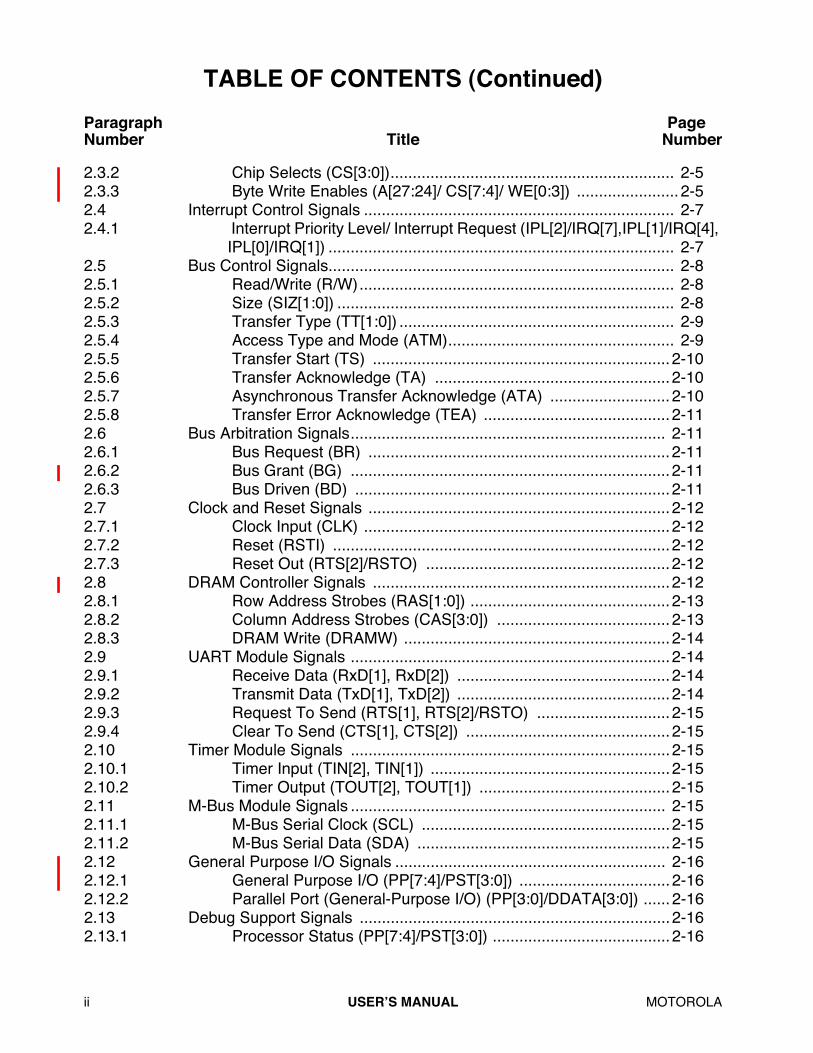
TABLE OF CONTENTS (Continued)
Paragraph PageNumber Title Number
ii
USERÕS MANUAL
MOTOROLA
2.3.2 Chip Selects (CS[3:0])................................................................ 2-52.3.3 Byte Write Enables (A[27:24]/ CS[7:4]/ WE[0:3]) ....................... 2-52.4 Interrupt Control Signals ...................................................................... 2-72.4.1 Interrupt Priority Level/ Interrupt Request (IPL[2]/IRQ[7],IPL[1]/IRQ[4],
IPL[0]/IRQ[1]) .............................................................................. 2-72.5 Bus Control Signals.............................................................................. 2-82.5.1 Read/Write (R/W)....................................................................... 2-82.5.2 Size (SIZ[1:0]) ............................................................................ 2-82.5.3 Transfer Type (TT[1:0]) .............................................................. 2-92.5.4 Access Type and Mode (ATM)................................................... 2-92.5.5 Transfer Start (TS) ...................................................................2-102.5.6 Transfer Acknowledge (TA) .....................................................2-102.5.7 Asynchronous Transfer Acknowledge (ATA) ........................... 2-102.5.8 Transfer Error Acknowledge (TEA) ..........................................2-112.6 Bus Arbitration Signals....................................................................... 2-112.6.1 Bus Request (BR) ....................................................................2-112.6.2 Bus Grant (BG) ........................................................................2-112.6.3 Bus Driven (BD) .......................................................................2-112.7 Clock and Reset Signals ....................................................................2-122.7.1 Clock Input (CLK) .....................................................................2-122.7.2 Reset (RSTI) ............................................................................2-122.7.3 Reset Out (RTS[2]/RSTO) .......................................................2-122.8 DRAM Controller Signals ...................................................................2-122.8.1 Row Address Strobes (RAS[1:0]) .............................................2-132.8.2 Column Address Strobes (CAS[3:0]) .......................................2-132.8.3 DRAM Write (DRAMW) ............................................................2-142.9 UART Module Signals ........................................................................2-142.9.1 Receive Data (RxD[1], RxD[2]) ................................................2-142.9.2 Transmit Data (TxD[1], TxD[2]) ................................................2-142.9.3 Request To Send (RTS[1], RTS[2]/RSTO) ..............................2-152.9.4 Clear To Send (CTS[1], CTS[2]) ..............................................2-152.10 Timer Module Signals ........................................................................2-152.10.1 Timer Input (TIN[2], TIN[1]) ......................................................2-152.10.2 Timer Output (TOUT[2], TOUT[1]) ...........................................2-152.11 M-Bus Module Signals ....................................................................... 2-152.11.1 M-Bus Serial Clock (SCL) ........................................................2-152.11.2 M-Bus Serial Data (SDA) .........................................................2-152.12 General Purpose I/O Signals ............................................................. 2-162.12.1 General Purpose I/O (PP[7:4]/PST[3:0]) ..................................2-162.12.2 Parallel Port (General-Purpose I/O) (PP[3:0]/DDATA[3:0]) ...... 2-162.13 Debug Support Signals ......................................................................2-162.13.1 Processor Status (PP[7:4]/PST[3:0]) ........................................2-16

TABLE OF CONTENTS (Continued)
Paragraph PageNumber Title Number
MOTOROLA
USERÕS MANUAL
iii
2.13.2 Debug Data (PP[3:0]/DDATA[3:0])........................................... 2-172.13.3 Development Serial Clock (TRST/DSCLK) ..............................2-172.13.4 Break Point (TMS/BKPT) .........................................................2-172.13.5 Development Serial Input (TDI/DSI) .........................................2-182.13.6 Development Serial Output (TDO/DSO) ..................................2-182.14 JTAG Signals .....................................................................................2-182.14.1 Test Clock (TCK) ......................................................................2-182.14.2 Test Reset (TRST/DSCLK) ......................................................2-182.14.3 Test Mode Select (TMS/BKPT) ................................................2-192.14.4 Test Data Input (TDI/DSI) .........................................................2-192.14.5 Test Data Output (TDO/DSO) ..................................................2-192.15 Test Signals ........................................................................................2-192.15.1 Motorola Test Mode (MTMOD) ................................................2-192.15.2 High Impedance (HIZ) ..............................................................2-202.16 Signal Summary .................................................................................2-20
Section 3ColdFire Core
3.1 Processor Pipelines ..............................................................................3-13.2 Processor Register Description ............................................................3-23.2.1 User Programming Model ..........................................................3-23.2.1.1 Data Registers (D0ÐD7) .................................................3-23.2.1.2 Address Registers (A0ÐA6) ............................................3-23.2.1.3 Stack Pointer (A7) ...........................................................3-23.2.1.4 Program Counter (PC).....................................................3-23.2.1.5 Condition Code Register (CCR) ......................................3-33.2.2 Supervisor Programming Model .................................................3-43.2.2.1 Status Register ...............................................................3-43.2.2.2 Vector Base Register (VBR) ...........................................3-53.3 Exception Processing Overview ...........................................................3-53.4 Exception Stack Frame Definition ........................................................3-73.5 Processor Exceptions ...........................................................................3-83.5.1 Access Error Exception ..............................................................3-83.5.2 Address Error Exception ............................................................3-93.5.3 Illegal Instruction Exception ........................................................3-93.5.4 Privilege Violation .......................................................................3-93.5.5 Trace Exception .........................................................................3-93.5.6 Debug Interrupt ........................................................................3-103.5.7 RTE and Format Error Exceptions ...........................................3-103.5.8 TRAP Instruction Exceptions ....................................................3-103.5.9 Interrupt Exception ...................................................................3-10

TABLE OF CONTENTS (Continued)
Paragraph PageNumber Title Number
iv
USERÕS MANUAL
MOTOROLA
3.5.10 Fault-on-Fault Halt ...................................................................3-113.5.11 Reset Exception .......................................................................3-113.6 Instruction Execution Timing ..............................................................3-113.6.1 Timing Assumptions .................................................................3-123.6.2 MOVE Instruction Execution Times .........................................3-12
Section 4Instruction Cache
4.1 Features Of Instruction Cache .............................................................4-14.2 Instruction Cache Physical Organization .............................................4-14.3 Instruction Cache Operation ................................................................4-24.3.1 Interaction With Other Modules ..................................................4-34.3.2 Memory Reference Attributes ....................................................4-34.3.3 Cache Coherency and Invalidation ............................................4-34.3.4 Reset ..........................................................................................4-44.3.5 Cache Miss Fetch Algorithm/Line Fills .......................................4-44.4 Instruction Cache Programming Model ................................................4-54.4.1 Instruction Cache Registers Memory Map .................................4-54.4.2 Instruction Cache Register .........................................................4-64.4.2.1 Cache Control Register (CACR) .....................................4-64.4.2.2 Access Control Registers (ACR0, ACR1) ....................... 4-8
Section 5SRAM
5.1 SRAM Features ....................................................................................5-15.2 SRAM Operation ..................................................................................5-15.3 Programming Model .............................................................................5-15.3.1 SRAM Register Memory Map ....................................................5-15.3.2 SRAM Registers .........................................................................5-25.3.2.1 SRAM Base Address Register (RAMBAR) ..................... 5-25.3.3 SRAM Initialization .....................................................................5-35.3.4 Power Management ...................................................................5-4
Section 6Bus Operation
6.1 Features ...............................................................................................6-16.2 Bus And Control Signals ......................................................................6-16.2.1 Address Bus (A[27:0]) ................................................................6-16.2.2 Data Bus (D[31:0]) ..................................................................... 6-2

TABLE OF CONTENTS (Continued)
Paragraph PageNumber Title Number
MOTOROLA
USERÕS MANUAL
v
6.2.3 Transfer Start (TS) .....................................................................6-26.2.4 Read/Write (R/W) .......................................................................6-26.2.5 Size (SIZ[1:0]) ............................................................................6-26.2.6 Transfer Type (TT[1:0]) ..............................................................6-26.2.7 Access Type and Mode (ATM) ...................................................6-36.2.8 Asynchronous Transfer Acknowledge (ATA) .............................6-36.2.9 Transfer Acknowledge (TA) ........................................................6-46.2.10 Transfer Error Acknowledge (TEA) ............................................6-46.3 Bus Exceptions .....................................................................................6-56.3.1 Double Bus Fault ........................................................................6-56.4 Bus Characteristics ..............................................................................6-56.5 Data Transfer Mechanism ....................................................................6-66.5.1 Bus Sizing ..................................................................................6-76.5.2 Bursting Read Transfers: Word, Longword, and Line ..............6-156.5.3 Bursting Write Transfers: Word, Longword, and Line ..............6-186.5.4 Burst-Inhibited Read Transfer: Word, Longword, and Line ......6-216.5.5 Burst-Inhibited Write Transfer: Word, Longword, and Line ......6-246.5.6 Asynchronous-Acknowledge Read Transfer ............................6-276.5.7 Asynchronous Acknowledge Write Transfer ............................6-306.5.8 Bursting Read Transfers with Asynchronous Acknowledge .....6-326.5.9 Bursting Write Transfers with Asynchronous Acknowledge .....6-356.5.10 Burst-Inhibited Read Transfers with Async. Acknowledge .......6-396.5.11 Burst-Inhibited Write Transfers with Async. Acknowledge .......6-426.5.12 Termination Tied to GND .........................................................6-456.6 Misaligned Operands .........................................................................6-466.7 Acknowledge Cycles ..........................................................................6-476.7.1 Interrupt Acknowledge Cycle ....................................................6-486.8 Bus Errors ..........................................................................................6-516.9 Bus Arbitration ....................................................................................6-536.9.1 Two Master Bus Arbitration Protocol (Two-Wire Mode) ...........6-536.9.2 External Bus Master Arbitration Protocol (Three-Wire Mode) ...6-616.10 Alternate Bus Master Operation .........................................................6-676.10.1 Alternate Master Read Transfer (MCF5206 Termination).........6-686.10.2 Alternate Master Write Transfer (MCF5206 Termination) .........6-716.10.3 Alternate Master Bursting Read (MCF5206 Termination) ........6-736.10.4 Alternate Master Bursting Write (MCF5206 Termination) .........6-766.11 Reset Operation .................................................................................6-806.11.1 Master Reset ............................................................................6-806.11.2 Normal Reset ...........................................................................6-826.11.3 Software Watchdog Timer Reset Operation .............................6-83
Section 7

TABLE OF CONTENTS (Continued)
Paragraph PageNumber Title Number
vi
USERÕS MANUAL
MOTOROLA
System Integration Module
7.1 Introduction .......................................................................................... 7-17.1.1 Features .....................................................................................7-17.2 SIM Operation ......................................................................................7-17.2.1 Module Base Address Register (MBAR) ....................................7-17.2.2 Bus Time-Out Monitor ................................................................7-27.2.3 Spurious Interrupt Monitor ..........................................................7-27.2.4 Software Watchdog Timer.......................................................... 7-37.2.5 Interrupt Controller .....................................................................7-37.3 Programming Model .............................................................................7-67.3.1 SIM Registers Memory Map .......................................................7-67.3.2 SIM Registers .............................................................................7-77.3.2.1 Module Base Address Register (MBAR) ........................ 7-77.3.2.2 SIM Configuration Register (SIMR) ................................7-97.3.2.3 Interrupt Control Register (ICR) ......................................7-97.3.2.4 Interrupt Mask Register (IMR) ......................................7-117.3.2.5 Interrupt-Pending Register (IPR) ..................................7-127.3.2.6 Reset Status Register (RSR) ........................................7-137.3.2.7 System Protection Control Register (SYPCR) .............. 7-147.3.2.8 Software Watchdog Interrupt Vector Reg. (SWIVR)...... 7-157.3.2.9 Software Watchdog Service Register (SWSR) ............. 7-167.3.2.10 Pin Assignment Register (PAR) ...................................7-16
Section 8Chip-Select Module
8.1 Introduction ..........................................................................................8-18.1.1 Features .....................................................................................8-18.2 Chip Select Module I/O ........................................................................8-18.2.1 Control Signals ...........................................................................8-18.2.1.1 Chip Select (CS[7:0]) ......................................................8-18.2.1.2 Write Enable (WE[3:0]) ...................................................8-18.2.1.3 Address Bus ...................................................................8-38.2.1.4 Data Bus .........................................................................8-48.2.1.5 Transfer Acknowledge (TA) ............................................8-48.3 Chip Select Operation ..........................................................................8-48.3.1 Chip Select Bank Definition ........................................................8-58.3.1.1 Base Address and Address Masking ..............................8-58.3.1.2 Access Permissions .......................................................8-68.3.1.3 Control Features .............................................................8-6

TABLE OF CONTENTS (Continued)
Paragraph PageNumber Title Number
MOTOROLA
USERÕS MANUAL
vii
8.3.1.3.1 8-, 16-, and 32-Bit Port Sizing ....................................................8-78.3.1.3.2 Termination ................................................................................8-78.3.1.3.3 Bursting Control ..........................................................................8-78.3.1.3.4 Address Setup and Hold Control ................................................8-88.3.2 Global Chip Select Operation .....................................................8-88.3.3 General Chip Select Operation ..................................................8-88.3.3.1 NonBurst Transfer with No Address Setup and Hold .....8-98.3.3.2 NonBurst Transfer with Address Setup ........................8-108.3.3.3 NonBurst Transfer With Address Setup and Hold ........8-128.3.3.4 Burst Transfer ...............................................................8-148.3.3.5 Burst Transfer With Address Setup ..............................8-168.3.3.6 Burst Transfer With Address Setup and Hold ...............8-188.3.4 Alternate Master Chip Select Operation ...................................8-218.3.4.1 Alternate Master NonBurst Transfer .............................8-218.3.4.2 Alternate Master Burst Transfer ....................................8-238.3.4.3 Alternate Master Burst Transfer With Address Setup and Hold
.......................................................................................8-258.4 Programming Model ...........................................................................8-278.4.1 Chip Select Registers Memory Map......................................... 8-278.4.2 Chip Select Controller Registers ..............................................8-298.4.2.1 Chip Select Address Register (CSAR0 - CSAR7) ........8-298.4.2.2 Chip Select Mask Register (CSMR0 - CSMR7)............ 8-308.4.2.3 Chip Select Control Register (CSCR0 - CSCR7) .........8-328.4.2.4 Default MemoryControl Register (DMCR) ....................8-38
Section 9Parallel Port (General-Purpose I/O) Module
9.1 Introduction ...........................................................................................9-19.2 Parallel Port Operation .........................................................................9-19.3 Programming Model .............................................................................9-19.3.1 Parallel Port Registers Memory Map ..........................................9-19.3.2 Parallel Port Registers ................................................................9-29.3.2.1 Port A Data Direction Register (PADDR) ........................9-29.3.2.2 Port A Data Register (PADAT) .......................................9-2
Section 10 DRAM Controller
10.1 Introduction .........................................................................................10-110.1.1 Features ...................................................................................10-110.2 DRAM Controller I/O ..........................................................................10-1

TABLE OF CONTENTS (Continued)
Paragraph PageNumber Title Number
viii
USERÕS MANUAL
MOTOROLA
10.2.1 Control Signals .........................................................................10-110.2.1.1 Row Address Strobes (RAS[0], RAS[1]) ....................... 10-110.2.1.2 Column Address Strobes (CAS[0:3]).............................10-210.2.1.3 DRAM Write (DRAMW) ................................................10-310.2.2 Address Bus .............................................................................10-310.2.3 Data Bus ..................................................................................10-410.3 DRAM Controller Operation ...............................................................10-410.3.1 Reset Operation .......................................................................10-410.3.1.1 Master Reset ................................................................10-510.3.1.2 Normal Reset ................................................................10-510.3.2 Definition of DRAM Banks ........................................................10-510.3.2.1 Base Address and Address Masking ............................10-510.3.2.2 Access Permissions .....................................................10-710.3.2.3 Timing ...........................................................................10-810.3.2.4 Page Mode ...................................................................10-810.3.2.5 Port Size/Page Size ......................................................10-810.3.2.6 Address Multiplexing ....................................................10-810.3.3 Normal Mode Operation .........................................................10-1510.3.3.1 NonBurst Transfer In Normal Mode ............................10-1610.3.3.2 Burst Transfer In Normal Mode ..................................10-1810.3.4 Fast Page Mode Operation ....................................................10-2010.3.4.1 Burst Transfer In Fast Page Mode .............................10-2110.3.4.2 Page Hit Read Transfer In Fast Page Mode .............. 10-2310.3.4.3 Page Hit Write Transfer in Fast Page Mode ............... 10-2510.3.4.4 Page Miss Transfer in Fast Page Mode ..................... 10-2710.3.4.5 Bus Arbitration ............................................................10-3010.3.5 Burst Page Mode Operation ...................................................10-3210.3.6 Extended Data-Out (EDO) DRAM Operation ......................... 10-3510.3.7 Refresh Operation ..................................................................10-3810.3.8 External Master Use of the DRAM Controller ........................ 10-4010.3.8.1 External Master Non-Burst Transfer in Normal Mode
.....................................................................................10-4110.3.8.2 External Master Burst Transfer in Normal Mode ........ 10-4410.3.8.3 External Master Burst Transfer in Burst Page Mode ..10-4710.3.8.4 Limitations ..................................................................10-5010.4 Programming Model .........................................................................10-5110.4.1 DRAM Controller Registers Memory Map ..............................10-5110.4.2 DRAM Controller Registers ....................................................10-5110.4.2.1 DRAM Controller Refresh Register (DCRR) ............... 10-5110.4.2.2 DRAM Controller Timing Register (DCTR) ................. 10-5210.4.2.3 DRAM Controller Address Reg. (DCAR0 - DCAR1) ... 10-5810.4.2.4 DRAM Controller Mask Reg. (DCMR0 - DCMR1) ....... 10-59

TABLE OF CONTENTS (Continued)
Paragraph PageNumber Title Number
MOTOROLA
USERÕS MANUAL
ix
10.4.2.5 DRAM Controller Control Reg. (DCCR0 - DCCR1) .....10-6010.5 DRAM Initialization Example ............................................................10-61
Section 11UART Modules
11.1 Module Overview.................................................................................11-211.1.1 Serial Communication Channel.................................................11-211.1.2 Baud-Rate Generator/Timer......................................................11-311.1.3 Interrupt Control Logic...............................................................11-311.2 UART Module Signal Definitions .........................................................11-311.2.1 Transmitter Serial Data Output (TxD)........................................11-311.2.2 Receiver Serial Data Input (RxD) ..............................................11-411.2.3 Request-to-Send (RTS).............................................................11-411.2.4 Clear-to-Send (CTS) .................................................................11-411.3 Operation.............................................................................................11-511.3.1 Baud-Rate Generator/Timer......................................................11-511.3.2 Transmitter and Receiver Operating Modes .............................11-611.3.2.1 Transmitter.....................................................................11-611.3.2.2 Receiver.........................................................................11-911.3.2.3 FIFO Stack...................................................................11-1111.3.3 Looping Modes........................................................................11-1211.3.3.1 Automatic Echo Mode..................................................11-1211.3.3.2 Local Loopback Mode..................................................11-1211.3.3.3 Remote Loopback Mode..............................................11-1311.3.4 Multidrop Mode........................................................................11-1411.3.5 Bus Operation .........................................................................11-1611.3.5.1 Read Cycles ................................................................11-1611.3.5.2 Write Cycles.................................................................11-1611.3.5.3 Interrupt Acknowledge Cycles .....................................11-1611.4 Register Description and Programming ............................................11-1611.4.1 Register Description ................................................................11-1611.4.1.1 Mode Register 1 (UMR1).............................................11-1711.4.1.2 Mode Register 2 (UMR2).............................................11-1911.4.1.3 Status Register (USR) .................................................11-2111.4.1.4 Clock Select Register (UCSR).....................................11-2411.4.1.5 Command Register (UCR)...........................................11-2411.4.1.6 Receiver Buffer (URB) .................................................11-2711.4.1.7 Transmitter Buffer (UTB) .............................................11-2811.4.1.8 Input Port Change Register (UIPCR)...........................11-2811.4.1.9 Auxiliary Control Register (UACR)...............................11-2911.4.1.10 Interrupt Status Register (UISR)..................................11-29
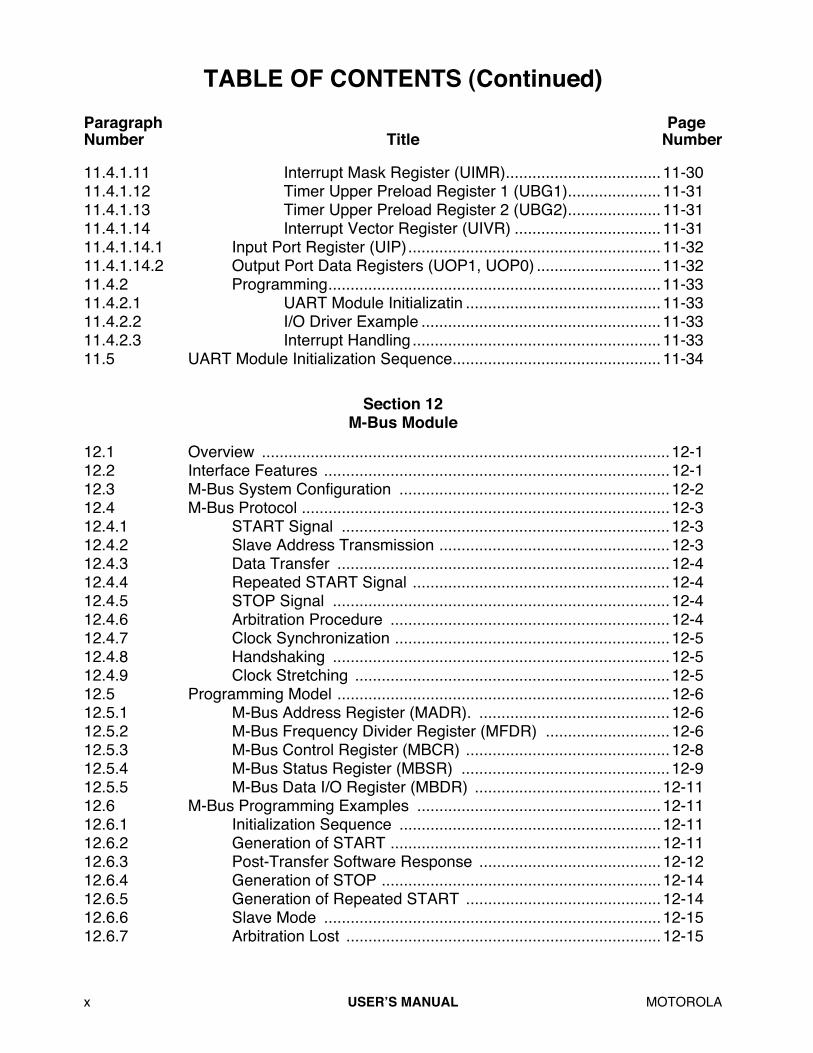
TABLE OF CONTENTS (Continued)
Paragraph PageNumber Title Number
x
USERÕS MANUAL
MOTOROLA
11.4.1.11 Interrupt Mask Register (UIMR)...................................11-3011.4.1.12 Timer Upper Preload Register 1 (UBG1)..................... 11-3111.4.1.13 Timer Upper Preload Register 2 (UBG2)..................... 11-3111.4.1.14 Interrupt Vector Register (UIVR) .................................11-3111.4.1.14.1 Input Port Register (UIP).........................................................11-3211.4.1.14.2 Output Port Data Registers (UOP1, UOP0) ............................11-3211.4.2 Programming...........................................................................11-3311.4.2.1 UART Module Initializatin ............................................11-3311.4.2.2 I/O Driver Example ......................................................11-3311.4.2.3 Interrupt Handling ........................................................11-3311.5 UART Module Initialization Sequence...............................................11-34
Section 12M-Bus Module
12.1 Overview ............................................................................................12-112.2 Interface Features ..............................................................................12-112.3 M-Bus System Configuration .............................................................12-212.4 M-Bus Protocol ...................................................................................12-312.4.1 START Signal ..........................................................................12-312.4.2 Slave Address Transmission ....................................................12-312.4.3 Data Transfer ...........................................................................12-412.4.4 Repeated START Signal ..........................................................12-412.4.5 STOP Signal ............................................................................12-412.4.6 Arbitration Procedure ...............................................................12-412.4.7 Clock Synchronization ..............................................................12-512.4.8 Handshaking ............................................................................12-512.4.9 Clock Stretching .......................................................................12-512.5 Programming Model ...........................................................................12-612.5.1 M-Bus Address Register (MADR). ...........................................12-612.5.2 M-Bus Frequency Divider Register (MFDR) ............................12-612.5.3 M-Bus Control Register (MBCR) ..............................................12-812.5.4 M-Bus Status Register (MBSR) ...............................................12-912.5.5 M-Bus Data I/O Register (MBDR) ..........................................12-1112.6 M-Bus Programming Examples .......................................................12-1112.6.1 Initialization Sequence ...........................................................12-1112.6.2 Generation of START .............................................................12-1112.6.3 Post-Transfer Software Response .........................................12-1212.6.4 Generation of STOP ...............................................................12-1412.6.5 Generation of Repeated START ............................................12-1412.6.6 Slave Mode ............................................................................12-1512.6.7 Arbitration Lost .......................................................................12-15
TABLE OF CONTENTS (Continued)
Paragraph PageNumber Title Number
MOTOROLA
USERÕS MANUAL
xi
Section 13Timer Module
13.1 Overview of the Timer Module ...........................................................13-113.2 Overview of Key Features ..................................................................13-113.3 Understanding the General-Purpose Timer Units ..............................13-213.3.1 Selecting the Prescaler ............................................................13-313.3.2 Working with Capture Mode .....................................................13-313.3.3 Configuring the Timer for Reference Compare ........................13-313.3.4 Configuring the Timer for Output Mode ....................................13-313.3.5 Interrupts ...................................................................................13-313.4 Programming Model ...........................................................................13-413.4.1 Understanding the General-Purpose Timer Registers .............13-413.4.1.1 Timer Mode Register (TMR) .........................................13-513.4.1.2 Timer Reference Register (TRR) ..................................13-613.4.1.3 Timer Capture Register (TCR) ......................................13-613.4.1.4 Timer Counter (TCN) ....................................................13-613.4.1.5 Timer Event Register (TER) .........................................13-7
Section 14Debug Support
14.1 Real-Time Trace..................................................................................14-114.2 Background Debug Mode....................................................................14-414.2.1 CPU Halt ...................................................................................14-514.2.2 BDM Serial Interface .................................................................14-614.2.3 BDM Command Set ..................................................................14-714.2.3.1 BDM Command Set Summary ......................................14-714.2.3.2 ColdFire BDM Commands.............................................14-814.2.3.3 Command Sequence Diagram ......................................14-914.2.3.4 Command Set Descriptions .........................................14-10

TABLE OF CONTENTS (Continued)
Paragraph PageNumber Title Number
xii
USERÕS MANUAL
MOTOROLA
14.2.3.4.1 Read A/D Register (RAREG/RDREG) ....................................14-1114.2.3.4.2 Write A/D Register (WAREG/WDREG)...................................14-1214.2.3.4.3 Read Memory Location (READ)..............................................14-1314.2.3.4.4 Write Memory Location (WRITE) ............................................14-1514.2.3.4.5 Dump Memory Block (DUMP).................................................14-1714.2.3.4.6 Fill Memory Block (FILL) .........................................................14-2014.2.3.4.7 Resume Execution (GO) .........................................................14-2114.2.3.4.8 No Operation (NOP)................................................................14-2214.2.3.4.9 Read Control Register (RCREG) ............................................14-2214.2.3.4.10 Write Control Register (WCREG)............................................14-2414.2.3.4.11 Read Debug Module Register (REMREG)..............................14-2414.2.3.4.12 Write Debug Module Register (WDMREG).............................14-2514.2.3.4.13 Unassigned Opcodes..............................................................14-2614.3 Real-Time Debug Support ................................................................14-2714.3.1 Programming Model................................................................14-2714.3.1.1 Address Breakpoint Registers (ABLR, ABHR) ............ 14-2814.3.1.2 Address Attribute Breakpoint Register (AATR) ........... 14-2814.3.1.3 Program Counter Breakdown Register (PBR, PBMR) 14-3014.3.1.4 Data Breakpoint Register (DBR, DBMR)..................... 14-3014.3.1.5 Trigger Definition Register (TDR) ................................14-3114.3.1.6 Configuration/Status Register (CSR)...........................14-3314.3.2 Theory of Operation ................................................................14-3514.3.2.1 Reuse of Debug Module Hardware .............................14-3714.3.3 Concurrent BDM and Processor Operation ............................14-3714.4 Motorola Recommended BDM Pinout...............................................14-3814.4.1 Differences Between the ColdFire BDM and a CPU32 BDM..14-38
Section 15IEEE 1149.1 Test Access Port (JTAG)
15.1 Overview ............................................................................................15-215.2 JTAG Pin Descriptions .......................................................................15-215.3 JTAG Register Descriptions ...............................................................15-315.3.1 JTAG Instruction Shift Register ...............................................15-315.3.1.1 EXTEST Instruction ......................................................15-315.3.1.2 ID Code ........................................................................15-415.3.1.3 SAMPLE/PRELOAD Instruction ................................... 15-415.3.1.4 HIGHZ Instruction .........................................................15-415.3.1.5 CLAMP Instruction ........................................................15-515.3.1.6 BYPASS Instruction ......................................................15-515.3.2 ID Code Register ......................................................................15-515.3.3 JTAG Boundary-Scan Register ................................................15-6
TABLE OF CONTENTS (Continued)
Paragraph PageNumber Title Number
MOTOROLA
USERÕS MANUAL
xiii
15.3.4 JTAG Bypass Register ...........................................................15-1015.4 TAP Controller ..................................................................................15-1015.5 Restrictions .......................................................................................15-1215.6 Disabling the IEEE 1149.1 Standard Operation ...............................15-1215.7 Motorola MCF5206 BSDL Description .............................................15-1315.8 Obtaining the IEEE 1149.1 Standard ...............................................15-13
Section 16Electrical Characteristics
16.1 Maximum Ratings ...............................................................................16-116.1.1 Supply, Input Voltage and Storage Temperature .....................16-116.1.2 Operating Temperature ............................................................16-116.1.3 Thermal Resistance .................................................................16-216.1.4 Output Loading .........................................................................16-216.2 DC Electrical Specifications ...............................................................16-216.3 AC Electrical Specifications ................................................................16-316.3.1 Clock Input Timing Specifications ............................................16-316.3.2 Clock Input Timing Diagram .....................................................16-316.3.3 Processor Bus Input Timing Specifications ..............................16-416.3.4 Input Timing Waveform Diagram ..............................................16-416.3.5 Processor Bus Output Timing Specifications ...........................16-516.3.6 Output Timing Waveform Diagram ...........................................16-616.3.7 Processor Bus Timing Diagrams ..............................................16-716.3.8 Timer Module AC Timing Specifications ................................16-1316.3.9 Timer Module Timing Diagram ...............................................16-1316.3.10 UART Module AC Timing Specifications ................................16-1416.3.11 UART Module Timing Diagram ..............................................16-1416.3.12 M-Bus Module AC Timing Specifications ...............................16-1516.3.12.1 Input Timing Specifications Between SCL and SDA ...16-1516.3.12.2 Output Timing Specifications Between SCL and SDA 16-1516.3.12.3 Timing Specifications Between CLK and SCL, SDA ...16-1616.3.13 M-Bus Module Timing Diagram ..............................................16-1616.3.14 General Purpose I/O Port AC Timing Specifications ..............16-1716.3.15 General Purpose I/O Port Timing Diagram ............................16-1716.3.16 IEEE 1149.1 (JTAG) AC Timing Specifications ......................16-1816.3.17 IEEE 1149.1 (JTAG) Timing Diagram ....................................16-18
Section 17 Mechanical Data

TABLE OF CONTENTS (Continued)
Paragraph PageNumber Title Number
xiv
USERÕS MANUAL
MOTOROLA
Appendix AMcF5206 Memory Map Summary
Appendix BPorting From M68K Architecture
B.1 C Compilers and Host Software........................................................... B-1B.2 Target Software Port ............................................................................B-1B.3 Initialization Code .................................................................................B-2B.4 Exception Handlers ..............................................................................B-2B.5 Supervisor Registers ............................................................................B-3
MOTOROLA
MCF5206 USERÕS MANUAL Rev 1.0
xv
LIST OF ILLUSTRATIONS
Figure PageNumber Title Number
1-1. MCF5206 Block Diagram................................................................................. 1-41-2. Programming Model......................................................................................... 1-7
3-1. ColdFire Processor Core Pipelines .................................................................. 3-13-2. User Programming Model ................................................................................3-33-3. Supervisor Programming Mode ....................................................................... 3-43-4. Status Register................................................................................................. 3-43-5. Exception Stack Frame Form........................................................................... 3-7
4-1. Instruction Cache Block Diagram......................................................................4-2
6-1. Signal Relationships to CLK............................................................................. 6-66-2. Internal Operand Representation..................................................................... 6-76-3. MCF5206 Interface to Various Port Sizes........................................................ 6-86-4. Byte-, Word-, and Longword-Read Transfer Flowchart ................................. 6-106-5. Longword-Read Transfer From a 32-Bit Port (No Wait States) ..................... 6-116-6. Byte-, Word-, and Longword-Write Transfer Flowchart ..................................6-136-7. Word-Write Transfer to a 16-Bit Port (No Wait States) .................................. 6-146-8. Bursting Word-, Longword-, and Line-Read Transfer Flowchart.................... 6-166-9. Bursting Word-Read From an 8-Bit Port (No Wait States)............................. 6-176-10. Word-, Longword-, and Line-Write Transfer Flowchart ...................................6-196-11. Line-Write Transfer to a 32-Bit Port (No Wait States) ....................................6-206-12. Burst-Inhibited Word-, Longword-, and Line-Read Transfer Flowchart.......... 6-226-13. Burst-Inhibited Longword Read From an 8-Bit Port (No Wait States) ............6-236-14. Burst-Inhibited Byte-, Word-, and Longword-Write Transfer Flowchart .........6-256-15. Burst-Inhibited Longword-Write Transfer to a 16-Bit Port
(No Wait States) .............................................................................................6-266-16. Byte-, Word-, and Longword-Read Transfer with Asynchronous Termination Flow-
chart (One Wait State) ...................................................................................6-286-17. Byte-Read Transfer from an 8-Bit Port Using Asynchronous Termination (One Wait
State) .............................................................................................................6-296-18. Byte-, Word-, and Longword-Write Transfer with Asynchronous Termination Flow-
chart ...............................................................................................................6-306-19. Byte-Write Transfer to a 32-Bit Port Using Asynchronous Termination (One Wait
State) .............................................................................................................6-31
Date: 8-31-98Revision No.: 1.1Pages affected: See change bars

LIST OF ILLUSTRATIONS (Continued)
Figure PageNumber Title Number
xvi
MCF5206 USERÕS MANUAL Rev 1.0
MOTOROLA
6-20. Bursting Word-, Longword-, and Line-Read Transfer with Asynchronous Termination Flowchart .......................................................................................................6-33
6-21. Bursting Longword-Read from 16-Bit Port Using Asynchronous Termination (One Wait State) .....................................................................................................6-34
6-22. Word-, Longword-, and Line-Write Transfer Flowchart with Asynchronous Termina-tion .................................................................................................................6-36
6-23. Bursting Line-Write from 32-Bit Port Using Asynchronous Termination (One Wait State) .............................................................................................................6-37
6-24. Burst-Inhibited Word-, Longword-, and Line-Read Transfer with Asynchronous Ter-mination Flowchart .........................................................................................6-40
6-25. Burst-Inhibited Word Read from 8-Bit Port Using Asynchronous Termination .............................................................................................................................6-41
6-26. Burst-Inhibited Word-, Longword-, and Line-Write Transfer with Asynchronous Ter-mination Flowchart .........................................................................................6-43
6-27. Burst-Inhibited Longword-Write Transfer to 16-Bit Port Using Asynchronous Termi-nation (One Wait State) .................................................................................6-44
6-28. Example of a Misaligned Longword Transfer .................................................6-466-29. Example of a Misaligned Word Transfer........................................................ 6-466-30. Interrupt-Acknowledge Cycle Flowchart ........................................................6-496-31. Interrupt Acknowledge Bus Cycle Timing (No Wait States) ........................... 6-506-32. Bursting Longword-Read Access from 16-Bit Port Terminated with TEA Timing
........................................................................................................................6-526-33. MCF5206 Two-Wire Mode Bus Arbitration Interface .....................................6-546-34. Two-Wire Implicit and Explicit Bus Ownership............................................... 6-566-35. Two-Wire Bus Arbitration with Bus Lock Negated .........................................6-576-36. Two-Wire Bus Arbitration with Bus Lock Bit Asserted ...................................6-586-37. MCF5206 Two-Wire Bus Arbitration Protocol State Diagram ........................ 6-596-38. Three-Wire Implicit and Explicit Bus Ownership ............................................6-626-39. Three-Wire Bus Arbitration with Bus Lock Bit Asserted .................................6-646-40. MCF5206 Bus Arbitration Protocol State Diagram ........................................6-656-41. Alternate Master Read Transfer using MCF5206-Generated
Transfer Acknowledge Flowchart ...................................................................6-696-42. Alternate Master Read Transfer Using MCF5206 Transfer Acknowledge Timing (No
Wait States) ...................................................................................................6-706-43. Alternate Master Write Transfer Using MCF5206-Generated
Transfer Acknowledge Flowchart ...................................................................6-716-44. Alternate Master Write Transfer Using MCF5206 Transfer-Acknowledge Timing (No
Wait States) ...................................................................................................6-726-45. Alternate Master Bursting Read Transfer Using MCF5206-Generated Transfer-Ac-
knowledge Flowchart .....................................................................................6-746-46. Alternate Master Bursting Longword Read Transfer to an 8-Bit Port Using MCF5206
Transfer-Acknowledge Timing (No Wait States) ............................................6-75

LIST OF ILLUSTRATIONS (Continued)
Figure PageNumber Title Number
MOTOROLA
MCF5206 USERÕS MANUAL Rev 1.0
xvii
6-47. Alternate Master Bursting Write Transfer using MCF5206-Generated Transfer-Ac-knowledge Flowchart .....................................................................................6-78
6-48. Alternate Master Bursting Longword Write Transfer to a 16-Bit Port Using MCF5206 Transfer Acknowledge Timing (No Wait States) ............................................6-79
6-49. Master Reset Timing ......................................................................................6-816-50. Normal Reset Timing .....................................................................................6-826-51. Software Watchdog Timer Reset Timing .......................................................6-83
8-1. MCF5206 Interface to Various Port Sizes ........................................................8-48-2. Longword Write Transfer from a 32-Bit Port (No Wait State, No Address Setup, No
Address Hold) ..................................................................................................8-98-3. Word Write Transfer to a 16-Bit Port (One Wait State, Address Setup, No Address
Hold) ...............................................................................................................8-118-4. Byte Write Transfer from an 8-Bit Port (One Wait State, Address Setup, Address
Hold) ...............................................................................................................8-138-5. Longword Burst Read Transfer from a 16-Bit Port (No Wait States,
No Address Setup, No Address Hold) ............................................................8-158-6. Longword Burst Read Transfer from a 16-Bit Port (No Wait States, Address Setup,
No Address Hold) ...........................................................................................8-178-7. Word Burst Read Transfer from an 8-Bit Port (No Wait States, Address Setup, Ad-
dress Hold) .....................................................................................................8-198-8. Alternate Master Longword Read Transfer from a 32-Bit Port (No Wait State, No Ad-
dress Setup, No Address Hold) ......................................................................8-228-9. Alternate Master Longword Read Transfer from a 16-bit Port (no wait state, no ad-
dress setup, no address hold) ........................................................................8-248-10. Alternate Master Longword Read Transfer from a 16-Bit Port (No Wait State, With
Address Setup Or Read Address Hold) .........................................................8-268-11. Chip-Select and Write-Enable Assertion with ASET = 0 Timing ....................8-358-12. Chip-Select and Write-Enable Assertion with ASET = 1Timing .....................8-358-13. Address Hold Timing with WRAH = 0 ............................................................8-368-14. Address Hold Timing with WRAH = 1 ............................................................8-368-15. Address Hold Timing with RDAH = 0 .............................................................8-378-16. Address Hold Timing with RDAH = 1 .............................................................8-388-17. Default Memory Address Hold Timing with WRAH = 0 ..................................8-418-18. Default Memory Address Hold Timing with WRAH = 1 ..................................8-428-19. Default Memory Address Hold Timing with RDAH = 0 ...................................8-438-20. Default Memory Address Hold Timing with RDAH = 1 ...................................8-43
10-1. MCF5206 Interface to Various Port Sizes...................................................... 10-410-2. Address Multiplexing For 8-bit DRAM With 512 byte Page Size.................... 10-910-3. Connection Diagram for 4 MByte DRAM with 8-bit Port and 1 KByte Page 10-15
LIST OF ILLUSTRATIONS (Continued)
Figure PageNumber Title Number
xviii
MCF5206 USERÕS MANUAL Rev 1.0
MOTOROLA
10-4. Connection Diagram for 1MByte DRAM with 8-bit Port and 1 KByte Page .10-1510-5. Byte Read Transfers in Normal Mode with 8-bit DRAM ...............................10-1710-6. Longword Write Transfer in Normal Mode with 16-bit DRAM ...................... 10-1910-7. Word Write Transfer in Fast Page Mode with 8-bit DRAM .......................... 10-2210-8. Longword Read Transfer Followed by a Page Hit Longword Read Transfer in Fast
Page Mode with 32-bit DRAM ......................................................................10-2410-9. Word Write Transfer Followed by a Page Hit Word Write Transfer in Fast Page Mode
with 16-bit DRAM .........................................................................................10-2610-10. Byte Read Transfer Followed by a Page Miss Byte Read Transfer in Fast Page Mode
with 8-bit DRAM ...........................................................................................10-2810-11. Bus Arbitration in Fast Page Mode ..............................................................10-3110-12. Longword Write Transfer Followed by a Word Read Transfer in Burst Page Mode
with 16-bit DRAM .........................................................................................10-3310-13. Word Read Transfer Followed by a Page Miss Byte Read Transfer in Fast Page
Mode with 8-bit EDO DRAM ........................................................................10-3610-14. Alternate Master Byte Read Transfer Followed by Byte Write Transfer in Normal
Mode with 16-bit DRAM ...............................................................................10-4210-15. Alternate Master Longword Write Transfer in Normal Mode with 16-bit DRAM
......................................................................................................................10-4510-16. Alternate Master Word Read Transfer in Burst Page Mode with 8-bit DRAM
......................................................................................................................10-4810-17. Normal Mode DRAM Transfer Timing ..........................................................10-5410-18. Fast Page Mode or Burst Page Mode DRAM Transfer Timing .................... 10-5410-19. Fast Page Mode or Burst Page Mode DRAM Transfer Timing .................... 10-5510-20. Fast Page Mode Page Hit and Page Miss DRAM Transfer Timing ............. 10-5610-21. Fast Page Mode or Burst Page Mode EDO DRAM Transfer Timing ........... 10-5710-22. CAS before RAS Refresh Cycle Timing .......................................................10-58
11-1. UART Block Diagram......................................................................................11-111-2. External and Internal Interface Signals ...........................................................11-411-3. Baud-Rate Timer Generator Diagram.............................................................11-511-4. Transmitter and Receiver Functional Diagram ...............................................11-711-5. Transmitter Timing Diagram ...........................................................................11-811-6. Receiver Timing Diagram .............................................................................11-1011-7. Looping Modes Functional Diagram .............................................................11-1311-8. Multidrop Mode Timing Diagram...................................................................11-1511-9. UART Software Flowchart ............................................................................11-35
LIST OF ILLUSTRATIONS (Continued)
Figure PageNumber Title Number
MOTOROLA
MCF5206 USERÕS MANUAL Rev 1.0
xix
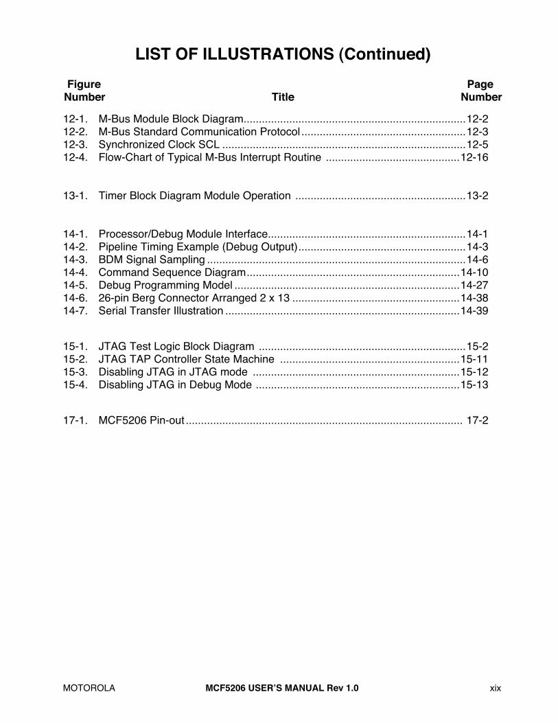
12-1. M-Bus Module Block Diagram.........................................................................12-212-2. M-Bus Standard Communication Protocol ......................................................12-312-3. Synchronized Clock SCL ................................................................................12-512-4. Flow-Chart of Typical M-Bus Interrupt Routine ............................................12-16
13-1. Timer Block Diagram Module Operation ........................................................13-2
14-1. Processor/Debug Module Interface.................................................................14-114-2. Pipeline Timing Example (Debug Output).......................................................14-314-3. BDM Signal Sampling .....................................................................................14-614-4. Command Sequence Diagram......................................................................14-1014-5. Debug Programming Model ..........................................................................14-2714-6. 26-pin Berg Connector Arranged 2 x 13 .......................................................14-3814-7. Serial Transfer Illustration .............................................................................14-39
15-1. JTAG Test Logic Block Diagram ....................................................................15-215-2. JTAG TAP Controller State Machine ...........................................................15-1115-3. Disabling JTAG in JTAG mode ....................................................................15-1215-4. Disabling JTAG in Debug Mode ...................................................................15-13
17-1. MCF5206 Pin-out ........................................................................................... 17-2
MOTOROLA
MCF5206
USERÕS MANUAL Rev 1.0
xxi
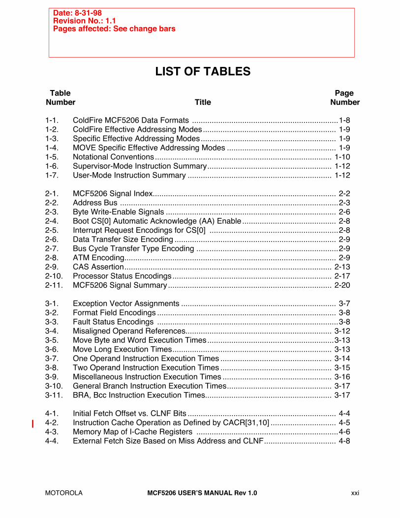
LIST OF TABLES
Table PageNumber Title Number
1-1. ColdFire MCF5206 Data Formats ...................................................................1-81-2. ColdFire Effective Addressing Modes............................................................. 1-91-3. Specific Effective Addressing Modes.............................................................. 1-91-4. MOVE Specific Effective Addressing Modes .................................................. 1-91-5. Notational Conventions................................................................................. 1-101-6. Supervisor-Mode Instruction Summary......................................................... 1-121-7. User-Mode Instruction Summary .................................................................. 1-12
2-1. MCF5206 Signal Index.................................................................................... 2-22-2. Address Bus ....................................................................................................2-32-3. Byte Write-Enable Signals .............................................................................. 2-62-4. Boot CS[0] Automatic Acknowledge (AA) Enable........................................... 2-82-5. Interrupt Request Encodings for CS[0] ...........................................................2-82-6. Data Transfer Size Encoding .......................................................................... 2-92-7. Bus Cycle Transfer Type Encoding .................................................................2-92-8. ATM Encoding................................................................................................. 2-92-9. CAS Assertion............................................................................................... 2-132-10. Processor Status Encodings......................................................................... 2-172-11. MCF5206 Signal Summary........................................................................... 2-20
3-1. Exception Vector Assignments ....................................................................... 3-73-2. Format Field Encodings .................................................................................. 3-83-3. Fault Status Encodings ...................................................................................3-83-4. Misaligned Operand References................................................................... 3-123-5. Move Byte and Word Execution Times..........................................................3-133-6. Move Long Execution Times......................................................................... 3-133-7. One Operand Instruction Execution Times ................................................... 3-143-8. Two Operand Instruction Execution Times ................................................... 3-153-9. Miscellaneous Instruction Execution Times .................................................. 3-163-10. General Branch Instruction Execution Times................................................ 3-173-11. BRA, Bcc Instruction Execution Times.......................................................... 3-17
4-1. Initial Fetch Offset vs. CLNF Bits .................................................................... 4-44-2. Instruction Cache Operation as Defined by CACR[31,10] .............................. 4-54-3. Memory Map of I-Cache Registers .................................................................4-64-4. External Fetch Size Based on Miss Address and CLNF................................. 4-8
Date: 8-31-98Revision No.: 1.1Pages affected: See change bars
LIST OF TABLES (Continued)
Figure PageNumber Title Number
xxii
MCF5206
USERÕS MANUAL Rev 1.0
MOTOROLA
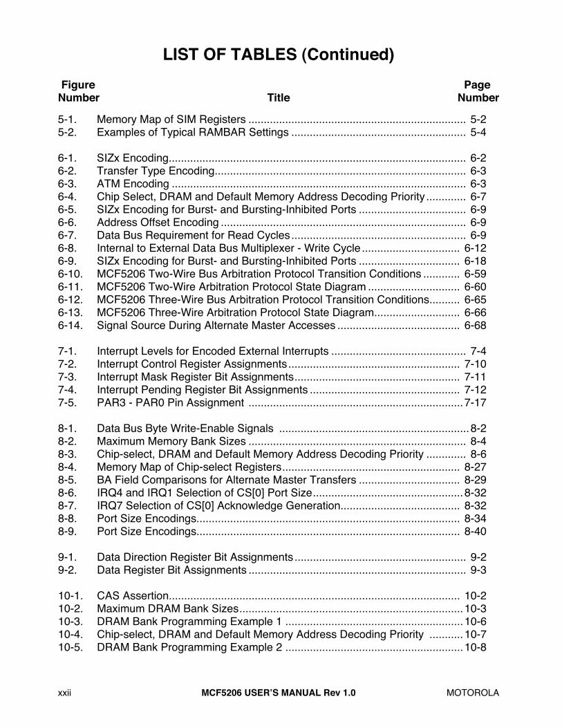
5-1. Memory Map of SIM Registers ....................................................................... 5-25-2. Examples of Typical RAMBAR Settings ......................................................... 5-4
6-1. SIZx Encoding................................................................................................. 6-26-2. Transfer Type Encoding.................................................................................. 6-36-3. ATM Encoding ................................................................................................ 6-36-4. Chip Select, DRAM and Default Memory Address Decoding Priority ............. 6-76-5. SIZx Encoding for Burst- and Bursting-Inhibited Ports ................................... 6-96-6. Address Offset Encoding ................................................................................ 6-96-7. Data Bus Requirement for Read Cycles ......................................................... 6-96-8. Internal to External Data Bus Multiplexer - Write Cycle ................................ 6-126-9. SIZx Encoding for Burst- and Bursting-Inhibited Ports ................................. 6-186-10. MCF5206 Two-Wire Bus Arbitration Protocol Transition Conditions ............ 6-596-11. MCF5206 Two-Wire Arbitration Protocol State Diagram .............................. 6-606-12. MCF5206 Three-Wire Bus Arbitration Protocol Transition Conditions.......... 6-656-13. MCF5206 Three-Wire Arbitration Protocol State Diagram............................ 6-666-14. Signal Source During Alternate Master Accesses ........................................ 6-68
7-1. Interrupt Levels for Encoded External Interrupts ............................................ 7-47-2. Interrupt Control Register Assignments ........................................................ 7-107-3. Interrupt Mask Register Bit Assignments...................................................... 7-117-4. Interrupt Pending Register Bit Assignments ................................................. 7-127-5. PAR3 - PAR0 Pin Assignment ......................................................................7-17
8-1. Data Bus Byte Write-Enable Signals ..............................................................8-28-2. Maximum Memory Bank Sizes ....................................................................... 8-48-3. Chip-select, DRAM and Default Memory Address Decoding Priority ............. 8-68-4. Memory Map of Chip-select Registers.......................................................... 8-278-5. BA Field Comparisons for Alternate Master Transfers ................................. 8-298-6. IRQ4 and IRQ1 Selection of CS[0] Port Size.................................................8-328-7. IRQ7 Selection of CS[0] Acknowledge Generation....................................... 8-328-8. Port Size Encodings...................................................................................... 8-348-9. Port Size Encodings...................................................................................... 8-40
9-1. Data Direction Register Bit Assignments ........................................................ 9-29-2. Data Register Bit Assignments ....................................................................... 9-3
10-1. CAS Assertion............................................................................................... 10-210-2. Maximum DRAM Bank Sizes.........................................................................10-310-3. DRAM Bank Programming Example 1 ..........................................................10-610-4. Chip-select, DRAM and Default Memory Address Decoding Priority ........... 10-710-5. DRAM Bank Programming Example 2 ..........................................................10-8
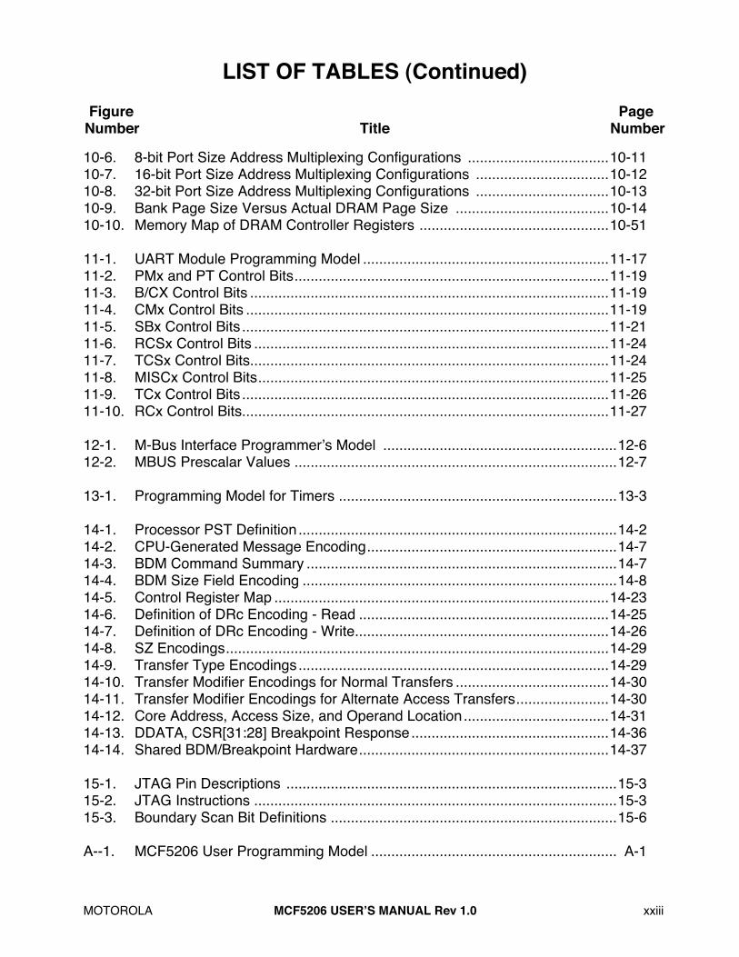
LIST OF TABLES (Continued)
Figure PageNumber Title Number
MOTOROLA
MCF5206 USERÕS MANUAL Rev 1.0
xxiii
10-6. 8-bit Port Size Address Multiplexing Configurations ...................................10-1110-7. 16-bit Port Size Address Multiplexing Configurations .................................10-1210-8. 32-bit Port Size Address Multiplexing Configurations .................................10-1310-9. Bank Page Size Versus Actual DRAM Page Size ......................................10-1410-10. Memory Map of DRAM Controller Registers ...............................................10-51
11-1. UART Module Programming Model .............................................................11-1711-2. PMx and PT Control Bits..............................................................................11-1911-3. B/CX Control Bits .........................................................................................11-1911-4. CMx Control Bits ..........................................................................................11-1911-5. SBx Control Bits ...........................................................................................11-2111-6. RCSx Control Bits ........................................................................................11-2411-7. TCSx Control Bits.........................................................................................11-2411-8. MISCx Control Bits.......................................................................................11-2511-9. TCx Control Bits ...........................................................................................11-2611-10. RCx Control Bits...........................................................................................11-27
12-1. M-Bus Interface ProgrammerÕs Model ..........................................................12-612-2. MBUS Prescalar Values ................................................................................12-7
13-1. Programming Model for Timers .....................................................................13-3
14-1. Processor PST Definition ...............................................................................14-214-2. CPU-Generated Message Encoding..............................................................14-714-3. BDM Command Summary .............................................................................14-714-4. BDM Size Field Encoding ..............................................................................14-814-5. Control Register Map ...................................................................................14-2314-6. Definition of DRc Encoding - Read ..............................................................14-2514-7. Definition of DRc Encoding - Write...............................................................14-2614-8. SZ Encodings...............................................................................................14-2914-9. Transfer Type Encodings.............................................................................14-2914-10. Transfer Modifier Encodings for Normal Transfers ......................................14-3014-11. Transfer Modifier Encodings for Alternate Access Transfers.......................14-3014-12. Core Address, Access Size, and Operand Location....................................14-3114-13. DDATA, CSR[31:28] Breakpoint Response.................................................14-3614-14. Shared BDM/Breakpoint Hardware..............................................................14-37
15-1. JTAG Pin Descriptions ..................................................................................15-315-2. JTAG Instructions ..........................................................................................15-315-3. Boundary Scan Bit Definitions .......................................................................15-6
A--1. MCF5206 User Programming Model ............................................................. A-1
MOTOROLA
MCF5206 USERÕS MANUAL Rev 1.0
1-1
2
3
4
5
6
7
8
9
10
11
12
13
14
15
16
1
SECTION 1INTRODUCTION
1.1 BACKGROUND
The MCF5206 integrated microprocessor combines a ColdFire
ª
processor core with several peripheral functions such as a DRAM controller, timers, general-purpose I/O and serial interfaces, debug module, and system integration. Designed for embedded control applications, the ColdFire core delivers enhanced performance while maintaining low system costs. To speed program execution, the on-chip instruction cache and SRAM provide one-cycle access to critical code and data. The MCF5206 greatly reduces the time required for system design and implementation by packaging common system functions on- chip and providing glueless interfaces to 8-, 16-, and 32-bit DRAM, SRAM, ROM, and I/O devices.
The revolutionary ColdFire microprocessor architecture gives cost-sensitive, high-volume applications new levels of price and performance. Based on the concept of variable-length RISC technology, ColdFire combines the architectural simplicity of conventional 32-bit RISC with a memory-saving, variable-length instruction set. The denser binary code for ColdFire processors consumes less valuable memory than any fixed-length instruction set RISC processor available. This improved code density means more efficient system memory use for a given application and requires slower, less costly memory to help achieve a target performance level.
The integrated peripheral functions provide high performance and flexibility: The DRAM controller supports as much as 512 Mbytes of DRAM; support for both page-mode and extended-data-out DRAMs; programmable full duplex DUART and a separate I
2
C
1
-compatible Motorola bus (M-Bus interface). Two 16-bit general-purpose multimode timers provide separate input and output signals. For system protection, the processor includes a programmable 16-bit software watchdog timer and several bus monitors. In addition, common system functions such as chip-selects, interrupt control, bus arbitration, and IEEE 1149.1 Test (JTAG) support are included.
A sophisticated debug interface supports both background-debug mode and real-time trace. This interface is common to all ColdFire-based processors and allows common emulator support across the entire ColdFire family.
1.2 MCF5206 FEATURES
The primary features of the MCF5206 integrated processor include the following:
1.
I
2
C
is a trademark of Phillips.
DATE: 9-1-98
REVISION NO.: 0.1
PAGES AFFECTED: SEE CHANGE BARS

Introduction
1-2
MCF5206 USERÕS MANUAL Rev 1.0
MOTOROLA
2
3
4
6
7
8
9
1
11
12
13
14
15
16
¥ ColdFire Processor Core
Ñ Variable-length RISCÑ 32-bit internal address bus with 28 bit external busÑ Chip Select and DRAM Ñ internal 32-bit decodingÑ 32-bit data busÑ 16 user-visible 32-bit wide registersÑ Supervisor / User modes for system protectionÑ Vector base register to relocate exception-vector tableÑ Optimized for high-level language constructsÑ 17 MIPS at 33 MHz
¥ 512 Byte Direct-mapped instruction cache
¥ 512 Byte on-chip SRAM
Ñ Provides one-cycle access to critical code and data
¥ DRAM Controller
Ñ Programmable refresh timer provides CAS-before-RAS refreshÑ Support for 2 separate memory banksÑ Support for page-mode DRAMs and extended-data-out (EDO) DRAMsÑ Allows external bus master access
¥ Dual Universal Synchronous/Asynchronous Receiver/Transmitter (DUART)
Ñ Full duplex operationÑ Baud-rate generatorÑ Modem control signals available (CTS, RTS)Ñ Processor-interrupt capability
¥ Dual 16-Bit General-Purpose Multimode Timers
Ñ 8-bit prescalerÑ Timer input and output pinsÑ 30ns resolution with 33 MHz system clockÑ Processor-interrupt capability
¥ Motorola Bus (M-Bus) Module
Ñ Interchip bus interface for EEPROMs, LCD controllers, A/D converters, keypads Ñ Compatible with industry-standard I
2
C BusÑ Master or slave modes support multiple mastersÑ Automatic interrupt generation with programmable level
¥ System Interface
Ñ Glueless bus interface to 8-, 16-, and 32-bit DRAM, SRAM, ROM, and I/O devicesÑ 8 programmable chip-select signalsÑ Programmable wait states and port sizesÑ Allows external bus masters to access chip-selectsÑ System protection

Introduction
MOTOROLA
MCF5206 USERÕS MANUAL Rev 1.0
1-3
¥ 16-bit software watchdog timer with prescaler¥ Double bus fault monitor¥ Bus timeout monitor¥ Spurious interrupt monitor
Ñ Programmable interrupt controller¥ Low interrupt latency¥ 3 external interrupt inputs¥ Programmable interrupt priority and autovector generator
Ñ IEEE 1149.1 test (JTAG) supportÑ 8-bit general-purpose I/O interface
¥ System Debug Support
Ñ Real-time traceÑ Background debug interface
¥ Fully Static 5.0-Volt Operation
¥ 160 Pin QFP Package
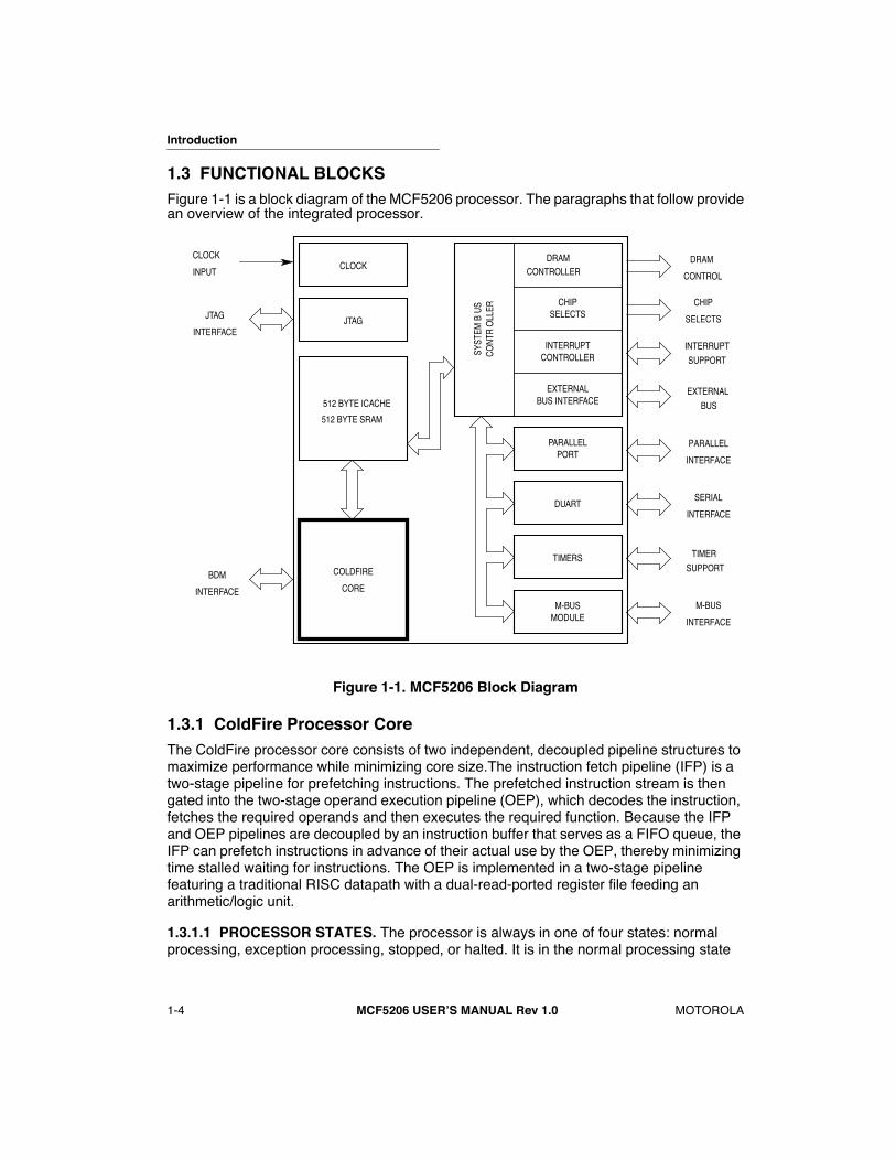
Introduction
1-4
MCF5206 USERÕS MANUAL Rev 1.0
MOTOROLA
2
3
4
6
7
8
9
1
11
12
13
14
15
16
1.3 FUNCTIONAL BLOCKS
Figure 1-1 is a block diagram of the MCF5206 processor. The paragraphs that follow providean overview of the integrated processor.
Figure 1-1. MCF5206 Block Diagram
1.3.1 ColdFire Processor Core
The ColdFire processor core consists of two independent, decoupled pipeline structures to maximize performance while minimizing core size.The instruction fetch pipeline (IFP) is a two-stage pipeline for prefetching instructions. The prefetched instruction stream is then gated into the two-stage operand execution pipeline (OEP), which decodes the instruction, fetches the required operands and then executes the required function. Because the IFP and OEP pipelines are decoupled by an instruction buffer that serves as a FIFO queue, the IFP can prefetch instructions in advance of their actual use by the OEP, thereby minimizing time stalled waiting for instructions. The OEP is implemented in a two-stage pipeline featuring a traditional RISC datapath with a dual-read-ported register file feeding an arithmetic/logic unit.
1.3.1.1 PROCESSOR STATES.
The processor is always in one of four states: normal processing, exception processing, stopped, or halted. It is in the normal processing state
DRAM
CHIP
INTERRUPT
CONTROLLER
EXTERNAL
DRAM
CONTROL
CHIP
SELECTS
INTERRUPT
SUPPORT
SERIAL
INTERFACE
CLOCK
INPUT
PARALLEL
TIMER
SUPPORTBDM
INTERFACE
BUS INTERFACE
CONTROLLER
SELECTS
PARALLELPORT
DUART
TIMERS
M-BUSMODULE
512 BYTE ICACHE
COLDFIRE
512 BYTE SRAM
CORE
JTAG
SYST
EM B
US
CO
NTR
OLL
ER
JTAG
INTERFACE
INTERFACE
M-BUS
INTERFACE
CLOCK
EXTERNAL
BUS

Introduction
MOTOROLA
MCF5206 USERÕS MANUAL Rev 1.0
1-5
when executing instructions, fetching instructions and operands, and storing instruction results.
Exception processing is the transition from program processing to system, interrupt, and exception handling; it includes fetching the exception vector, stacking operations, and refilling the instruction fetch pipe after an exception. The processor enters exception processing when an exceptional internal condition arises, such as tracing an instruction, an instruction resulting in a trap, or executing specific instructions; (External conditions, such as interrupts and access errors, also cause exceptions) and ends when the first instruction of the exception handler enters the operand execution pipeline.
Stopped mode is a reduced power operation mode that causes the processor to remain quiescent until either a reset or nonmasked interrupt occurs. The STOP instruction is used to enter this operation mode.
The processor halts when it receives an access error or generates an address error while in the exception processing state. For example, if during exception processing of one access error another access error occurs, the MCF5206 processor cannot complete the transition to normal processing nor can it save the internal machine state. The processor assumes that the system is not operational and halts. Only an external reset can restart a halted processor. When the processor executes a STOP instruction, it is in a special type of normal processing state, e.g., one without bus cycles. The processor stops but it does not halt.
The processor can also halt in a restart mode because of Background-Debug mode events.
1.3.1.2 PROGRAMMING MODEL.
The ColdFire programming model is separated into two privilege modes: supervisor and user. The S-bit in the status register (SR) indicates the current privilege mode. The processor identifies a logical address by accessing either the supervisor or user address space, which differentiates between supervisor and user modes.
User programs can access only registers specific to the user mode. System software executing in the supervisor mode can access all registers using the control registers to perform supervisory functions. User programs are thus restricted from accessing privileged information. The operating system performs management and service tasks for user programs by coordinating their activities. This difference allows the supervisor mode to protect system resources from uncontrolled accesses.
Most instructions execute in either mode but some instructions that have important system effects are privileged and can execute only in the supervisor mode. For instance, user programs cannot execute the STOP instructions. To prevent a program executing in user mode from entering the supervisor mode, instructions that can alter the S-bit in the SR are privileged. The TRAP instructions provide controlled access to operating system services for user programs.
When in normal processing, the processor employs the user mode and the user programming model . During exception processing, the processor changes from user to supervisor mode. The current SR value on the stack is saved and then the S-bit is set, forcing the processor into the supervisor mode. To return to the user mode, a system routine must execute a MOVE to SR, or an RTE, which operate in the supervisor mode, modifying
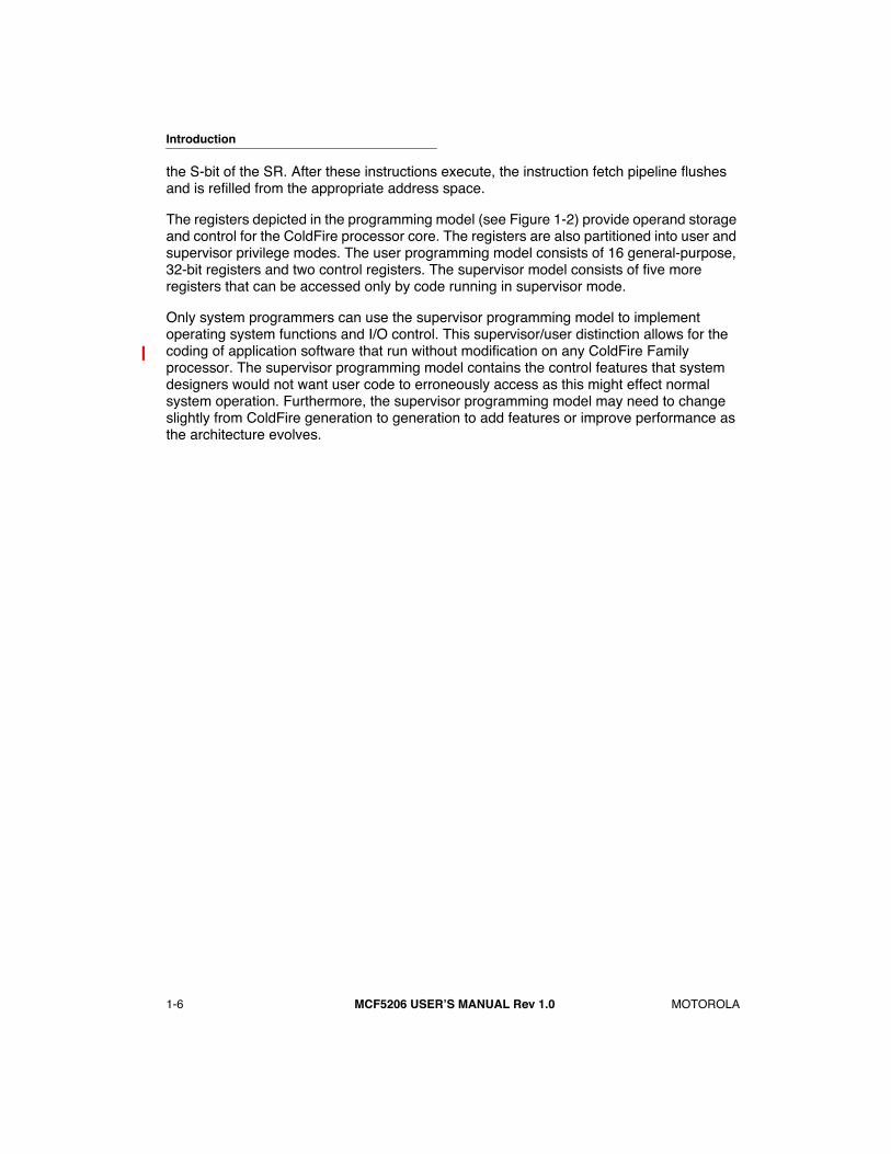
Introduction
1-6
MCF5206 USERÕS MANUAL Rev 1.0
MOTOROLA
2
3
4
6
7
8
9
1
11
12
13
14
15
16
the S-bit of the SR. After these instructions execute, the instruction fetch pipeline flushes and is refilled from the appropriate address space.
The registers depicted in the programming model (see Figure 1-2) provide operand storage and control for the ColdFire processor core. The registers are also partitioned into user and supervisor privilege modes. The user programming model consists of 16 general-purpose, 32-bit registers and two control registers. The supervisor model consists of five more registers that can be accessed only by code running in supervisor mode.
Only system programmers can use the supervisor programming model to implement operating system functions and I/O control. This supervisor/user distinction allows for the coding of application software that run without modification on any ColdFire Family processor. The supervisor programming model contains the control features that system designers would not want user code to erroneously access as this might effect normal system operation. Furthermore, the supervisor programming model may need to change slightly from ColdFire generation to generation to add features or improve performance as the architecture evolves.

Introduction
MOTOROLA
MCF5206 USERÕS MANUAL Rev 1.0
1-7
Figure 1-2. Programming Model
The user programming model includes eight data registers, seven address registers, and a stack pointer register. The address registers and stack pointer can be used as base address registers or software stack pointers, and any of the 16 registers can be used as index registers. Two control registers are available in the user mode: the program counter (PC), which contains the address of the instruction that the MCF5206 device is executing, and the lower byte of the SR, which is accessible as the Condition Code Register (CCR). The CCR contains the condition codes that reflect the results of a previous operation and can be used for conditional instruction execution in a program.
31 0
D0
D1
D2
DATAREGISTERS
D3
D4
D5
D6
D7
31 0
A0
A1
A2
ADDRESSREGISTERS
A3
A4
A5
A6
A7 STACK POINTER
PC PROGRAM COUNTER
CCR CONDITION CODE REGISTER
USER PROGRAMMING MODEL
15
31 19 (CCR) SR STATUS REGISTER
MUST BE ZEROS VBR VECTOR BASE REGISTER
CACR CACHE CONTROL REGISTER
ACR0 ACCESS CONTROL REGISTER 0
ACR1 ACCESS CONTROL REGISTER 1
SUPERVISOR PROGRAMMING MODEL

Introduction
1-8
MCF5206 USERÕS MANUAL Rev 1.0
MOTOROLA
2
3
4
6
7
8
9
1
11
12
13
14
15
16
The supervisor programming model includes the upper byte of the SR, which contains operation control information. The Vector Base Register (VBR) contains the upper 12 bits of the base address of the exception vector table, which is used in exception processing. The lower 20 bits of the VBR are forced to zero, allowing the vector table to reside on any 1 Mbyte memory boundary.
The Cache Control Register (CACR) controls enabling of the on-chip cache. Two access control registers (ACR1, ACR0) allow portions of the address space to be mapped as noncacheable
.
See subsections 4.3 and 4.4 for details on these registers
.
1.3.1.3 DATA FORMAT SUMMARY.
The processor performs all arithmetic using 2Õs complement, but operands can be signed or unsigned. Registers, memory, or instructions themselves can contain operands. The operand size for each instruction is either explicitly encoded in the instruction or implicitly defined by the instruction operation. Table1-1 summarizes the MCF5206 data formats.
1.3.1.4 ADDRESSING CAPABILITIES SUMMARY.
The MCF5206 processor supports seven addressing modes. The register indirect addressing modes support postincrement, predecrement, offset, and indexing, which are particularly useful for handling data structures common to sophisticated embedded applications and high-level languages. The program counter indirect mode also has indexing and offset capabilities. This addressing mode is typically required to support position-independent software. Besides these addressing modes, the MCF5206 processor provides index scaling features.
An instructionÕs addressing mode can specify the value of an operand or a register containing the operand. It can also specify how to derive the effective address of an operand in memory. Each addressing mode has an assembler syntax. Some instructions imply the addressing mode for an operand. These instructions include the appropriate fields for operands that use only one addressing mode. Table 1-2 summarizes the effective addressing modes of ColdFire processors. Table 1-3 summarizes the MOVE specific effective addressing modes.
1.3.1.5 NOTATIONAL CONVENTIONS.
Table 1-4 lists the notation conventions used throughout this manual, unless otherwise specified.
Table 1-1. ColdFire MCF5206 Data Formats
OPERAND DATA FORMAT SIZE
Bit 1-BitByte 8-BitsWord 16-Bits
Longword 32-Bits

Introduction
MOTOROLA
MCF5206 USERÕS MANUAL Rev 1.0
1-9
Table 1-2. ColdFire Effective Addressing Modes
ADDRESSING MODES SYNTAX
Register Direct Data
AddressDnAn
Register IndirectAddress
Address with PostincrementAddress with PredecrementAddress with Displacement
(An)(An)+Ð(An)
(d16,An)Address Register Indirect with Index
8-Bit Displacement (d8,An,Xi)
Program Counter Indirectwith Displacement (d16,PC)
Program Counter Indirect with Index 8-Bit Displacement (d8,PC,Xi)
Absolute Data Addressing ShortLong
(xxx).W(xxx).L
Immediate #<xxx>
Table 1-3. MOVE Specific Effective Addressing Modes
SOURCE <EA> DESTINATION <EA>
Dn AllAn All
(An) All(An)+ All-(An) All
(d
16
,An)
(d
16
,PC)
DnAn
(An)(An)+-(An)
(d
16
,An)
(d
8
,An,Xi)
(d
8
,PC,Xi)
DnAn
(An)(An)+-(An)
(xxx).W(xxx).L
DnAn
(An)(An)+-(An)
#<xxx>
DnAn
(An)(An)+-(An)

Introduction
1-10
MCF5206 USERÕS MANUAL Rev 1.0
MOTOROLA
2
3
4
6
7
8
9
1
11
12
13
14
15
16
Table 1-4. Notational Conventions
OPCODE WILDCARDS
cc Logical Condition (example: NE for not equal)
REGISTER OPERANDS
An Any Address Register n (example: A3 is address register 3)Ay,Ax Source and destination address registers, respectively
Dn Any Data Register n (example: D5 is data register 5)Dy,Dx Source and destination data registers, respectively
Rn Any Address or Data RegisterRy,Rx Any source and destination registers, respectively
Rw Any second destination registerRc Any Control Register (example VBR is the vector base register)
REGISTER/PORT NAMES
DDATA Debug Data PortCCR Condition Code Register (lower byte of status register)PC Program Counter
PST Processor Status PortSR Status Register
MISCELLANEOUS OPERANDS
#<data> Immediate data following the instruction word(s)<ea> Effective Address
<ea>y,<ea>x Source and Destination Effective Addresses, respectively<label> Assembly Program Label<list> List of registers (example: D3ÐD0)<size> Operand data size: Byte (B), Word (W), Longword (L)
OPERATIONS
+ Arithmetic addition or postincrement indicatorÐ Arithmetic subtraction or predecrement indicatorx Arithmetic multiplication/ Arithmetic division~ Invert; operand is logically complemented& Logical AND| Logical OR~ Logical exclusive OR
<< Shift left (example: D0 << 3 is shift D0 left 3 bits)>> Shift right (example: D0 >> 3 is shift D0 right 3 bits)
®
Source operand is moved to destination operand
¨
Two operands are exchangedsign-extended All bits of the upper portion are made equal to the high-order bit of the lower portionIf <condition>
then <operations>else <operations>
Test the condition. If true, the operations after ÔthenÕ are performed. If the condition is false and the optional ÔelseÕ clauseis present, the operations after ÔelseÕ are performed. If the condition is false and else is omitted, the instruction performs nooperation. Refer to the Bcc instruction description as an example.

Introduction
MOTOROLA
MCF5206 USERÕS MANUAL Rev 1.0
1-11
1.3.1.6 INSTRUCTION SET OVERVIEW.
The ColdFire instruction set supports high-level languages and is optimized for those instructions embedded code most commonly executes. Table 1-5 provides an alphabetized listing of the ColdFire instruction set opcode, operation, and syntax. The left operand in the syntax is always the source operand and the right operand is the destination operand.
SUBFIELDS AND QUALIFIERS
{} Optional Operation() Identifies an indirect addressd
n
Displacement Value, n-Bits Wide (example: d
16
is a 16-bit displacement)
Address Calculated Effective Address (pointer)Bit Bit Selection (example: Bit 3 of D0)
LSB Least Significant Bit (example: MSB of D0)LSW Least Significant WordMSB Most Significant BitMSW Most Significant Word
CONDITION CODE REGISTER BIT NAMES
P Branch Prediction Bit in CCRC Carry Bit in CCRN Negative Bit in CCRV Overflow Bit in CCRX Extend Bit in CCRZ Zero Bit in CCR
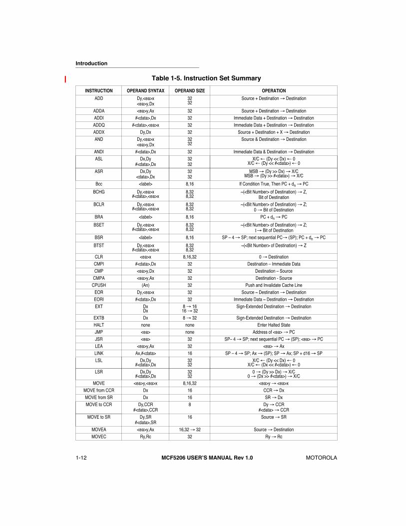
Introduction
1-12
MCF5206 USERÕS MANUAL Rev 1.0
MOTOROLA
2
3
4
6
7
8
9
1
11
12
13
14
15
16
Table 1-5. Instruction Set Summary
INSTRUCTION OPERAND SYNTAX OPERAND SIZE OPERATION
ADD Dy,<ea>x<ea>y,Dx
3232
Source + Destination
®
Destination
ADDA <ea>y,Ax 32 Source + Destination
®
DestinationADDI #<data>,Dx 32 Immediate Data + Destination
®
DestinationADDQ #<data>,<ea>x 32 Immediate Data + Destination
®
DestinationADDX Dy,Dx 32 Source + Destination + X
®
DestinationAND Dy,<ea>x
<ea>y,Dx3232
Source & Destination
®
Destination
ANDI #<data>,Dx 32 Immediate Data & Destination
®
DestinationASL Dx,Dy
#<data>,Dx3232
X/C
¬
(Dy << Dx)
¬
0X/C
¬
(Dy << #<data>)
¬
0
ASR Dx,Dy<data>,Dx
3232
MSB
®
(Dy >> Dx)
®
X/CMSB
®
(Dy >> #<data>)
®
X/C
Bcc <label> 8,16 If Condition True, Then PC + d
n
®
PC
BCHG Dy,<ea>x#<data>,<ea>x
8,328,32
~(<Bit Number> of Destination)
®
Z, Bit of Destination
BCLR Dy,<ea>x#<data>,<ea>x
8,328,32
~(<Bit Number> of Destination)
®
Z; 0
®
Bit of DestinationBRA <label> 8,16 PC + d
n
®
PC
BSET Dy,<ea>x#<data>,<ea>x
8,328,32
~(<Bit Number> of Destination)
®
Z;
1®
Bit of DestinationBSR <label> 8,16 SP Ð 4
®
SP; next sequential PC
®
(SP); PC + d
n
®
PC
BTST Dy,<ea>x#<data>,<ea>x
8,328,32
~(<Bit Number> of Destination)
®
Z
CLR <ea>x 8,16,32 0
®
DestinationCMPI #<data>,Dx 32 Destination Ð Immediate DataCMP <ea>y,Dx 32 Destination Ð Source
CMPA <ea>y,Ax 32 Destination - SourceCPUSH (An) 32 Push and Invalidate Cache Line
EOR Dy,<ea>x 32 Source ~ Destination
®
DestinationEORI #<data>,Dx 32 Immediate Data ~ Destination
®
DestinationEXT Dx
Dx8
®
1616
®
32Sign-Extended Destination
®
Destination
EXTB Dx 8
®
32 Sign-Extended Destination
®
DestinationHALT none none Enter Halted StateJMP <ea> none Address of <ea>
®
PCJSR <ea> 32 SPÐ 4
®
SP; next sequential PC
®
(SP); <ea>
®
PCLEA <ea>y,Ax 32 <ea>
®
AxLINK Ax,#<data> 16 SP Ð 4
®
SP; Ax
®
(SP); SP
®
Ax; SP + d16
®
SPLSL Dx,Dy
#<data>,Dx3232
X/C
¬
(Dy << Dx)
¬
0X/C
¬
(Dx << #<data>)
¬
0LSR Dx,Dy
#<data>,Dx3232
0
®
(Dy >> Dx)
®
X/C0
®
(Dx >> #<data>)
®
X/CMOVE <ea>y,<ea>x 8,16,32 <ea>y
®
<ea>xMOVE from CCR Dx 16 CCR
®
DxMOVE from SR Dx 16 SR
®
DxMOVE to CCR Dy,CCR
#<data>,CCR8 Dy
®
CCR#<data>
®
CCRMOVE to SR Dy,SR
#<data>,SR16 Source
®
SR
MOVEA <ea>y,Ax 16,32
®
32 Source
®
DestinationMOVEC Ry,Rc 32 Ry
®
Rc
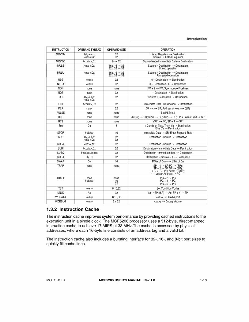
Introduction
MOTOROLA
MCF5206 USERÕS MANUAL Rev 1.0 1-13
1.3.2 Instruction CacheThe instruction cache improves system performance by providing cached instructions to the execution unit in a single clock. The MCF5206 processor uses a 512-byte, direct-mapped instruction cache to achieve 17 MIPS at 33 MHz.The cache is accessed by physical addresses, where each 16-byte line consists of an address tag and a valid bit.
The instruction cache also includes a bursting interface for 32-, 16-, and 8-bit port sizes to quickly fill cache lines.
MOVEM list,<ea>x<ea>y,list
3232
Listed Registers ® DestinationSource ® Listed Registers
MOVEQ #<data>,Dx 8 ® 32 Sign-extended Immediate Data® DestinationMULS <ea>y,Dx 16 x 16 ® 32
32 x 32 ® 32Source ´ Destination ® Destination
Signed operationMULU <ea>y,Dx 16 x 16 ® 32
32 x 32 ® 32Source ´ Destination ® Destination
Unsigned operationNEG <ea>x 32 0 Ð Destination ® Destination
NEGX <ea>x 32 0 Ð DestinationÐ X ® DestinationNOP none none PC + 2 ® PC; Synchronize PipelinesNOT <ea> 32 ~ Destination ® DestinationOR Dy,<ea>x
<ea>y,Dx32 Source | Destination ® Destination
ORI #<data>,Dx 32 Immediate Data | Destination ® DestinationPEA <ea> 32 SP Ð 4 ® SP; Address of <ea> ® (SP)
PULSE none none Set PST= $4RTE none none (SP+2) ® SR; SP+4 ® SP; (SP) ® PC; SP + FormatField ® SPRTS none none (SP) ® PC; SP + 4 ® SPScc Dx 8 If Condition True, Then 1's ® Destination;
Else 0's ® DestinationSTOP #<data> 16 Immediate Data ® SR; Enter Stopped StateSUB Dy,<ea>x
<ea>y,Dx3232
Destination - Source® Destination
SUBA <ea>y,Ax 32 Destination - Source® DestinationSUBI #<data>,Dx 32 Destination Ð Immediate Data ® DestinationSUBQ #<data>,<ea>x 32 Destination - Immediate data ® DestinationSUBX Dy,Dx 32 Destination Ð Source Ð X ® DestinationSWAP Dn 16 MSW of Dn ¬® LSW of DnTRAP none none SP Ð 4 ® SP;PC ® (SP);
SP Ð 2 ® SP;SR ® (SP);SP Ð 2 ® SP; Format ® (SP);
Vector Address ® PCTRAPF none
#<data>none1632
PC + 2 ® PCPC + 4 ® PCPC + 6 ® PC
TST <ea>y 8,16,32 Set Condition CodesUNLK Ax 32 Ax ®SP; (SP) ® Ax; SP + 4 ® SP
WDDATA <ea>y 8,16,32 <ea>y ®DDATA portWDEBUG <ea>y 2 x 32 <ea>y ® Debug Module
INSTRUCTION OPERAND SYNTAX OPERAND SIZE OPERATION
Introduction
1-14 MCF5206 USERÕS MANUAL Rev 1.0 MOTOROLA
2
3
4
6
7
8
9
1
11
12
13
14
15
16
1.3.3 Internal SRAMThe 512-byte on-chip SRAM provides one clock-cycle access for the ColdFire core. This SRAM can store processor stack and critical code or data segments to maximize performance.
1.3.4 DRAM ControllerThe MCF5206 DRAM controller provides a glueless interface for as many as two banks of DRAM, each of which can be from 128 Kbytes to 256 Mbytes in size. The controller supports an 8-, 16-, or 32-bit data bus. A unique addressing scheme allows for increases in system memory size without rerouting address lines and rewiring boards. The controller operates in fast page mode, burst-page mode, or normal mode, and supports extended-data-out (EDO) DRAMs.
DRAM operations are available to other external bus masters. The DRAM controller can generate CAS and RAS for an external master and can continue to manage refresh requests.
1.3.5 DUART ModuleA full duplex DUART module contains independent receivers and transmitters that can be clocked by the DUART internal timer. This timer is clocked by the system clock or an external clock supplied by the TIN pin. Data formats can be 5, 6, 7, or 8 bits with even, odd, or no parity, and as many as 2 stop bits in 1/16 increments. Four-byte receive buffers and two-byte transmit buffers minimize CPU service calls. The DUART module also provides several error-detection and maskable-interrupt capabilities. Modem support includes request-to-send (RTS) and clear-to-send (CTS) lines.
The system clock provides the clocking function via a programmable prescaler. You can select full duplex, autoecho loopback, local loopback, and remote loopback modes. The programmable DUART can interrupt the CPU on various normal or error-condition events.
1.3.6 Timer ModuleThe timer module includes two general-purpose timers, each of which contains a free-running 16-bit timer for use in any of three modes. One mode captures the timer value with an external event. Another mode triggers an external signal or interrupts the CPU when the timer reaches a set value, while a third mode counts external events. The timer unit has an 8-bit prescaler that allows for programming the clock input frequency, which is derived from the system clock. The programmable timer-output pin generates either an active-low pulse or toggles the output.
1.3.7 Motorola Bus (M-Bus) Module
The M-Bus interface is a two-wire, bidirectional serial bus that exchanges data between devices and is compatible with the I2C Bus standard. The M-Bus minimizes the interconnection between devices in the end system and is best suited for applications that need occasional bursts of rapid communication over short distances among several
Introduction
MOTOROLA MCF5206 USERÕS MANUAL Rev 1.0 1-15
devices. The number of devices that can be connected is limited by bus capacitance and the number of unique addresses.
1.3.8 System InterfaceThe MCF5206 processor provides a glueless interface to 8-, 16-, and 32-bit port size SRAM, ROM, and peripheral devices with independent programmable control of the assertion and negation of chip-selects and write-enables. Programmable address and data-hold times can be extended for a compatible interface to external devices and memory. The MCF5206 also supports bursting ROMs.
1.3.8.1 EXTERNAL BUS INTERFACE. The bus interface controller transfers information between the ColdFire core and memory, peripherals, or other masters on the external bus. The external bus interface provides as many as 28 bits of address bus space, a 32-bit data bus, and all associated control signals. This interface implements an extended synchronous protocol that supports bursting operations. For nonsynchronous external memory and peripherals, the MCF5206 processor provides an alternate asynchronous bus transfer acknowledgment signal.
Simple two-wire request/acknowledge bus arbitration between the MCF5206 processor and another bus master, such as a DMA device, is glueless with arbitration handled internal to the MCF5206 processor. Alternately, an external bus arbiter can control more complex three-wire (request, grant, busy) multiple-master bus arbitration, allowing overlapped bus arbitration with one clock-bus handovers.
1.3.8.2 CHIP-SELECTS . Eight programmable chip-select outputs provide signals that enable external memory and peripheral circuits for automatic wait-state insertion. These signals also interface to 8-, 16-, or 32-bit ports. In addition, other external bus masters can access chip-selects. The upper four chip-selects are multiplexed with A[27:24] of the address bus and the four write-enable signals. The base address, access permissions, and timing waveforms are all programmable with configuration registers.
1.3.9 8-Bit Parallel Port (General-Purpose I/O) An 8-bit general-purpose programmable parallel port serves as either an input or an output on a bit-by-bit basis. The parallel port is multiplexed with PST[3:0] and DDATA[3:0] debug signals.
1.3.10 Interrupt Controller The interrupt controller provides user-programmable control of three or seven external interrupt and five internal peripheral interrupts. You can program each internal interrupt to any one of seven interrupt levels and four priority levels within each of these levels. You can configure the three external interrupt signals as either fixed interrupt levels 1, 4, and 7, or as a seven-level encoded interrupt. You can program the external interrupts to any one of the four priority levels within the respective interrupt levels.

Introduction
1-16 MCF5206 USERÕS MANUAL Rev 1.0 MOTOROLA
2
3
4
6
7
8
9
1
11
12
13
14
15
16
1.3.11 System Protection The MCF5206 processor contains a 16-bit software watchdog timer with an 8-bit prescaler. The programmable software watchdog timer provides either a level 7 interrupt or a hardware reset on timeout. The MCF5206 processor also contains a reset status register that indicates the cause of the last reset.
1.3.12 JTAGTo help with system diagnostics and manufacturing testing, the MCF5206 processor includes dedicated user-accessible test logic that complies with the IEEE 1149.1 standard for boundary scan testability, often referred to as Joint Test Action Group, or JTAG. For more information, refer to the IEEE 1149.1 standard.
1.3.13 System Debug InterfaceThe ColdFire processor core debug interface supports real-time trace and Background-Debug Mode. A four-pin Background Debug Mode (BDM) interface provides system debug. The BDM is a proper subset of the BDM interface provided on MotorolaÕs 683XX Family of parts.
In real-time trace, four status lines provide information on processor activity in real time (PST pins). A 4-bit wide debug data bus (DDATA) displays operand data, which helps track the machineÕs dynamic execution path as the change-of-flow instructions execute. These signals are multiplexed with an 8-bit parallel port for application development, which does not use real-time trace.
1.3.14 Pinout and PackageThe MCF5206 device is supplied in a 160-pin plastic quad flat pack package.
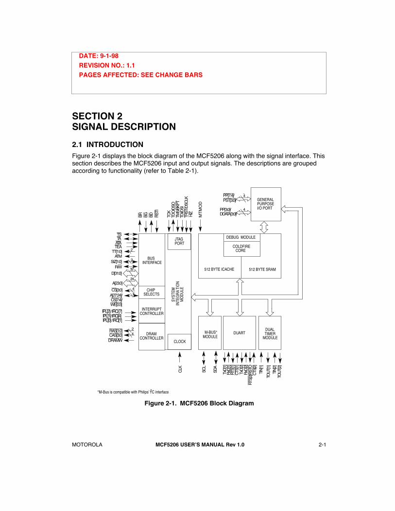
MOTOROLA
MCF5206 USERÕS MANUAL Rev 1.0
2-1
SECTION 2SIGNAL DESCRIPTION
2.1 INTRODUCTION
Figure 2-1 displays the block diagram of the MCF5206 along with the signal interface. This section describes the MCF5206 input and output signals. The descriptions are grouped according to functionality (refer to Table 2-1).
Figure 2-1. MCF5206 Block Diagram
TDO
/DSO
TDI/D
SI
TMS/
BKPT
TCK
CLK
SCL
SDA
TIN
[1]
TOU
T[1]
TA ATA TEA
R/W
SIZ[1:0]
D[31:0]
A[23:0]
IPL[2] / IRQ [7]IPL[1]/ IRQ[4] IPL[0] / IRQ[1]
TxD
[1]
RxD
[1]
RTS[
1]C
TS[1
]Tx
D[2
]R
xD[2
]RT
S[2]
/RST
OC
TS[2
]
RAS[1:0]CAS[3:0]DRAMW
24
24
32
A[27:24]/CS[7:4]/WE[0:3]
CS[3:0] 44
2ATM
TT[1:0]
TS
BR BG BD TRST
/DSC
LK
HIZ
RST
I
2
MT
MO
D
4PP[7:4]/PST[3:0]/
*M-Bus is compatible with PhilipsÕ I2C interface
4PP[3:0]/DDATA[3:0]/
TOU
T[2]
TIN
[2]
GENERALPURPOSEI/O PORT
BUSINTERFACE
JTAGPORT
CHIPSELECTS
INTERRUPTCONTROLLER
DRAMCONTROLLER
CLOCK
SYST
EMIN
TEG
RA
TIO
N
MO
DU
LE
M-BUS*MODULE
DUARTDUALTIMER
MODULE
512 BYTE SRAM512 BYTE ICACHE
COLDFIRECORE
DEBUG MODULE
DATE: 9-1-98
REVISION NO.: 1.1
PAGES AFFECTED: SEE CHANGE BARS
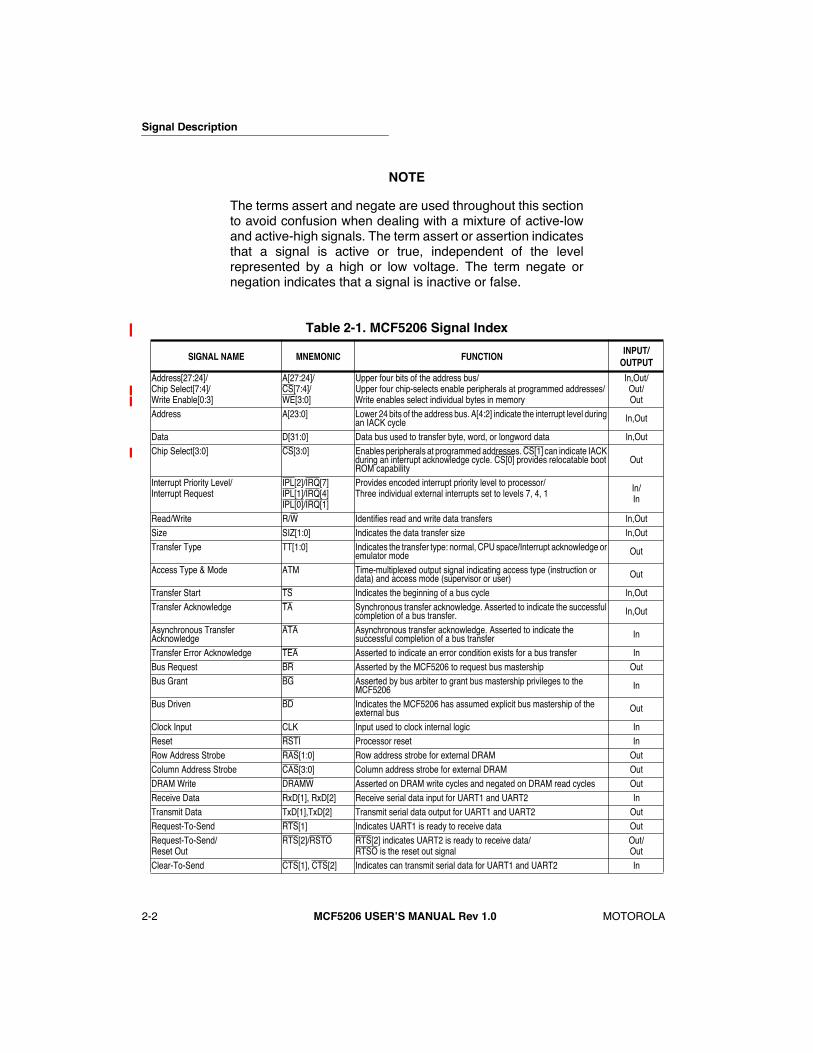
Signal Description
2-2
MCF5206 USERÕS MANUAL Rev 1.0
MOTOROLA
NOTE
The terms
assert
and
negate
are used throughout this sectionto avoid confusion when dealing with a mixture of active-lowand active-high signals. The term
assert
or
assertion
indicatesthat a signal is active or true, independent of the levelrepresented by a high or low voltage. The term
negate
or
negation
indicates that a signal is inactive or false.
Table 2-1. MCF5206 Signal Index
SIGNAL NAME MNEMONIC FUNCTIONINPUT/
OUTPUT
Address[27:24]/Chip Select[7:4]/Write Enable[0:3]
A[27:24]/CS[7:4]/WE[3:0]
Upper four bits of the address bus/ Upper four chip-selects enable peripherals at programmed addresses/Write enables select individual bytes in memory
In,Out/Out/Out
Address A[23:0] Lower 24 bits of the address bus. A[4:2] indicate the interrupt level during an IACK cycle In,Out
Data D[31:0] Data bus used to transfer byte, word, or longword data In,OutChip Select[3:0] CS[3:0] Enables peripherals at programmed addresses. CS[1] can indicate IACK
during an interrupt acknowledge cycle. CS[0] provides relocatable boot ROM capability
Out
Interrupt Priority Level/Interrupt Request
IPL[2]/IRQ[7]IPL[1]/IRQ[4]IPL[0]/IRQ[1]
Provides encoded interrupt priority level to processor/Three individual external interrupts set to levels 7, 4, 1 In/
In
Read/Write R/W Identifies read and write data transfers In,OutSize SIZ[1:0] Indicates the data transfer size In,OutTransfer Type TT[1:0] Indicates the transfer type: normal, CPU space/Interrupt acknowledge or
emulator mode Out
Access Type & Mode ATM Time-multiplexed output signal indicating access type (instruction or data) and access mode (supervisor or user) Out
Transfer Start TS Indicates the beginning of a bus cycle In,OutTransfer Acknowledge TA Synchronous transfer acknowledge. Asserted to indicate the successful
completion of a bus transfer. In,Out
Asynchronous Transfer Acknowledge
ATA Asynchronous transfer acknowledge. Asserted to indicate the successful completion of a bus transfer In
Transfer Error Acknowledge TEA Asserted to indicate an error condition exists for a bus transfer InBus Request BR Asserted by the MCF5206 to request bus mastership OutBus Grant BG Asserted by bus arbiter to grant bus mastership privileges to the
MCF5206 In
Bus Driven BD Indicates the MCF5206 has assumed explicit bus mastership of the external bus Out
Clock Input CLK Input used to clock internal logic InReset RSTI Processor reset InRow Address Strobe RAS[1:0] Row address strobe for external DRAM OutColumn Address Strobe CAS[3:0] Column address strobe for external DRAM OutDRAM Write DRAMW Asserted on DRAM write cycles and negated on DRAM read cycles OutReceive Data RxD[1], RxD[2] Receive serial data input for UART1 and UART2 InTransmit Data TxD[1],TxD[2] Transmit serial data output for UART1 and UART2 OutRequest-To-Send RTS[1] Indicates UART1 is ready to receive data OutRequest-To-Send/Reset Out
RTS[2]/RSTO RTS[2] indicates UART2 is ready to receive data/RTSO is the reset out signal
Out/Out
Clear-To-Send CTS[1], CTS[2] Indicates can transmit serial data for UART1 and UART2 In
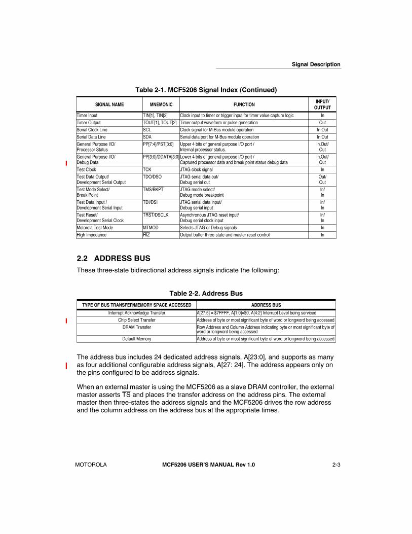
Signal Description
MOTOROLA
MCF5206 USERÕS MANUAL Rev 1.0
2-3
2.2 ADDRESS BUS
These three-state bidirectional address signals indicate the following:
The address bus includes 24 dedicated address signals, A[23:0], and supports as many as four additional configurable address signals, A[27: 24]. The address appears only on the pins configured to be address signals.
When an external master is using the MCF5206 as a slave DRAM controller, the external master asserts TS and places the transfer address on the address pins. The external master then three-states the address signals and the MCF5206 drives the row address and the column address on the address bus at the appropriate times.
Timer Input TIN[1], TIN[2] Clock input to timer or trigger input for timer value capture logic InTimer Output TOUT[1], TOUT[2] Timer output waveform or pulse generation OutSerial Clock Line SCL Clock signal for M-Bus module operation In,OutSerial Data Line SDA Serial data port for M-Bus module operation In,OutGeneral Purpose I/O/ Processor Status
PP[7:4]/PST[3:0] Upper 4 bits of general purpose I/O port /Internal processor status.
In.Out/Out
General Purpose I/O/ Debug Data
PP[3:0]/DDATA[3:0] Lower 4 bits of general purpose I/O port /Captured processor data and break point status debug data
In,Out/Out
Test Clock TCK JTAG clock signal InTest Data Output/Development Serial Output
TDO/DSO JTAG serial data out/Debug serial out
Out/Out
Test Mode Select/Break Point
TMS/BKPT JTAG mode select/Debug mode breakpoint
In/In
Test Data Input /Development Serial Input
TDI/DSI JTAG serial data input/Debug serial input
In/In
Test Reset/Development Serial Clock
TRST/DSCLK Asynchronous JTAG reset input/Debug serial clock input
In/In
Motorola Test Mode MTMOD Selects JTAG or Debug signals InHigh Impedance HIZ Output buffer three-state and master reset control In
Table 2-2. Address Bus
TYPE OF BUS TRANSFER/MEMORY SPACE ACCESSED ADDRESS BUS
Interrupt Acknowledge Transfer A[27:5] = $7FFFF, A[1:0]=$0, A[4:2] Interrupt Level being servicedChip Select Transfer Address of byte or most significant byte of word or longword being accessed
DRAM Transfer Row Address and Column Address indicating byte or most significant byte of word or longword being accessed
Default Memory Address of byte or most significant byte of word or longword being accessed
Table 2-1. MCF5206 Signal Index (Continued)
SIGNAL NAME MNEMONIC FUNCTIONINPUT/
OUTPUT
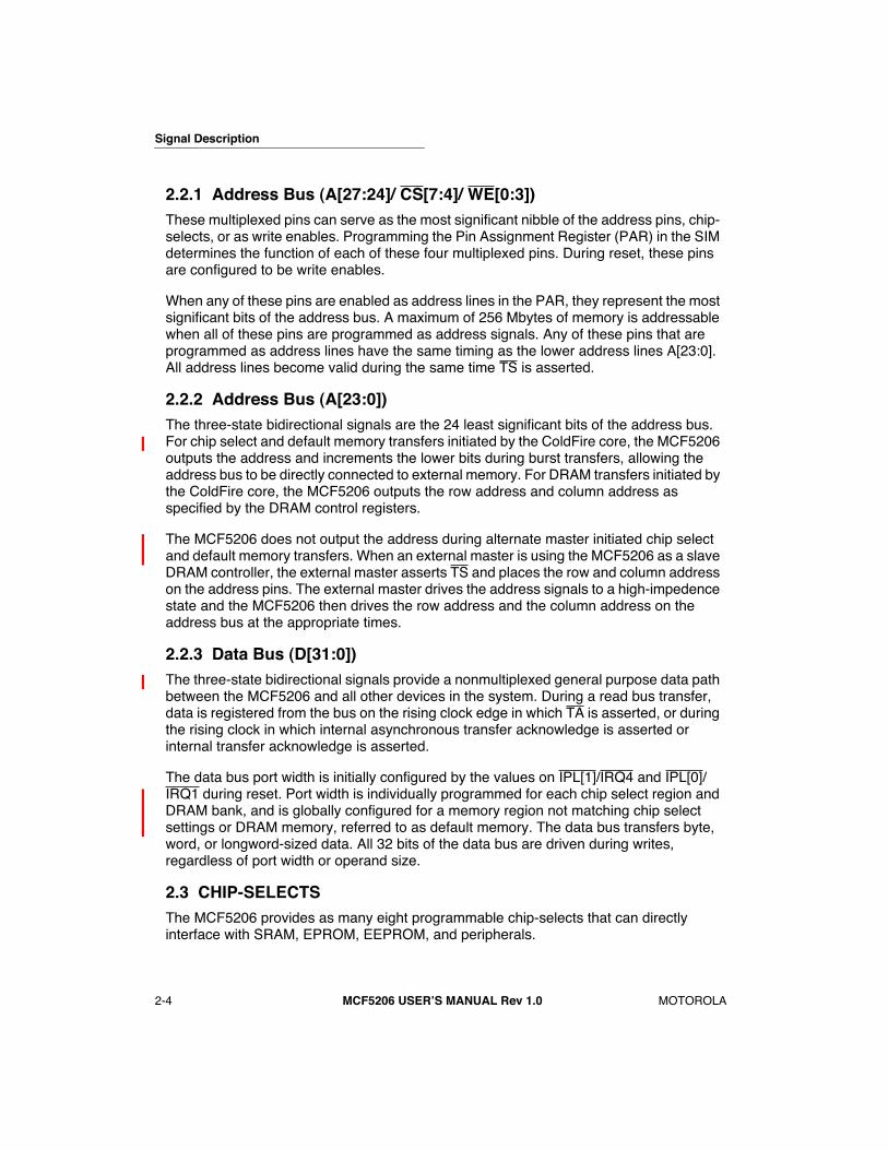
Signal Description
2-4
MCF5206 USERÕS MANUAL Rev 1.0
MOTOROLA
2.2.1 Address Bus (A[27:24]/ CS[7:4]/ WE[0:3])
These multiplexed pins can serve as the most significant nibble of the address pins, chip- selects, or as write enables. Programming the Pin Assignment Register (PAR) in the SIM determines the function of each of these four multiplexed pins. During reset, these pins are configured to be write enables.
When any of these pins are enabled as address lines in the PAR, they represent the most significant bits of the address bus. A maximum of 256 Mbytes of memory is addressable when all of these pins are programmed as address signals. Any of these pins that are programmed as address lines have the same timing as the lower address lines A[23:0]. All address lines become valid during the same time TS is asserted.
2.2.2 Address Bus (A[23:0])
The three-state bidirectional signals are the 24 least significant bits of the address bus. For chip select and default memory transfers initiated by the ColdFire core, the MCF5206 outputs the address and increments the lower bits during burst transfers, allowing the address bus to be directly connected to external memory. For DRAM transfers initiated by the ColdFire core, the MCF5206 outputs the row address and column address as specified by the DRAM control registers.
The MCF5206 does not output the address during alternate master initiated chip select and default memory transfers. When an external master is using the MCF5206 as a slave DRAM controller, the external master asserts TS and places the row and column address on the address pins. The external master drives the address signals to a high-impedence state and the MCF5206 then drives the row address and the column address on the address bus at the appropriate times.
2.2.3 Data Bus (D[31:0])
The three-state bidirectional signals provide a nonmultiplexed general purpose data path between the MCF5206 and all other devices in the system. During a read bus transfer, data is registered from the bus on the rising clock edge in which TA is asserted, or during the rising clock in which internal asynchronous transfer acknowledge is asserted or internal transfer acknowledge is asserted.
The data bus port width is initially configured by the values on IPL[1]/IRQ4 and IPL[0]/IRQ1 during reset. Port width is individually programmed for each chip select region and DRAM bank, and is globally configured for a memory region not matching chip select settings or DRAM memory, referred to as default memory. The data bus transfers byte, word, or longword-sized data. All 32 bits of the data bus are driven during writes, regardless of port width or operand size.
2.3 CHIP-SELECTS
The MCF5206 provides as many eight programmable chip-selects that can directly interface with SRAM, EPROM, EEPROM, and peripherals.
Signal Description
MOTOROLA
MCF5206 USERÕS MANUAL Rev 1.0
2-5
2.3.1 Chip-Selects (A[27:24]/ CS[7:4]/ WE[0:3])
These multiplexed pins can serve as the most significant nibble of the address pins, chip- selects, or as write enables. Programming the Pin Assignment Register (PAR) in the SIM determines the function of each of these four multiplexed pins. During reset, these pins are configured to be write-enables.
The active-low chip select output signals provide control for peripherals and memory. You can program each chip select for an address location, with masking capabilities, port size and burst-capability indication, wait-state generation, and internal/external termination. A reset disables these chip-selects.
2.3.2 Chip-Selects (CS[3:0])
These active-low output signals provide control for peripherals and memory. CS[3] and CS[2] are functionally equivalent to the upper order chip-selects previously described. However, CS[1] can also be programmed to assert during CPU space accesses including interrupt-acknowledge cycles. CS[0] provides a special function as a global chip select that lets you relocate boot ROM at any defined address space. CS[0] is the only chip select initialized during reset. Port size and termination (internal vs. external) for CS[0] are configured by the logic levels on IPL[2]/IRQ[7], IPL[1]/IRQ[4], and IPL[0]/IRQ[1] during reset.
2.3.3 Byte Write-Enables (A[27:24]/ CS[7:4]/ WE[0:3])
These multiplexed pins can serve as the most significant nibble of the address pins, chip- selects, or as write-enables. Programming the Pin Assignment Register (PAR) in the SIM determines the function of each of these four multiplexed pins. During reset, these pins are configured to be write-enables.
The active-low write-enable output signals provide control for peripherals and memory during write transfers. During write transfers, these outputs indicate which bytes within a longword transfer are being selected and which bytes of the data bus are used for the transfer. WE[0] controls D[31:24], WE[1] controls D[23:16], WE[2] controls D[15:8] and WE[3] controls D[7:0]. These generated signals provide byte data select signals that are decoded from the SIZ[1:0] and A[1:0] signals in addition to the programmed port size and burst capability of the memory being accessed, as shown in Table 2-3.
2.4 INTERRUPT CONTROL SIGNALS
The interrupt signals supply the external interrupt requests or interrupt level to the MCF5206. During reset, these pins configure the processor for the number of wait states and port size for the boot chip select (CS[0]).
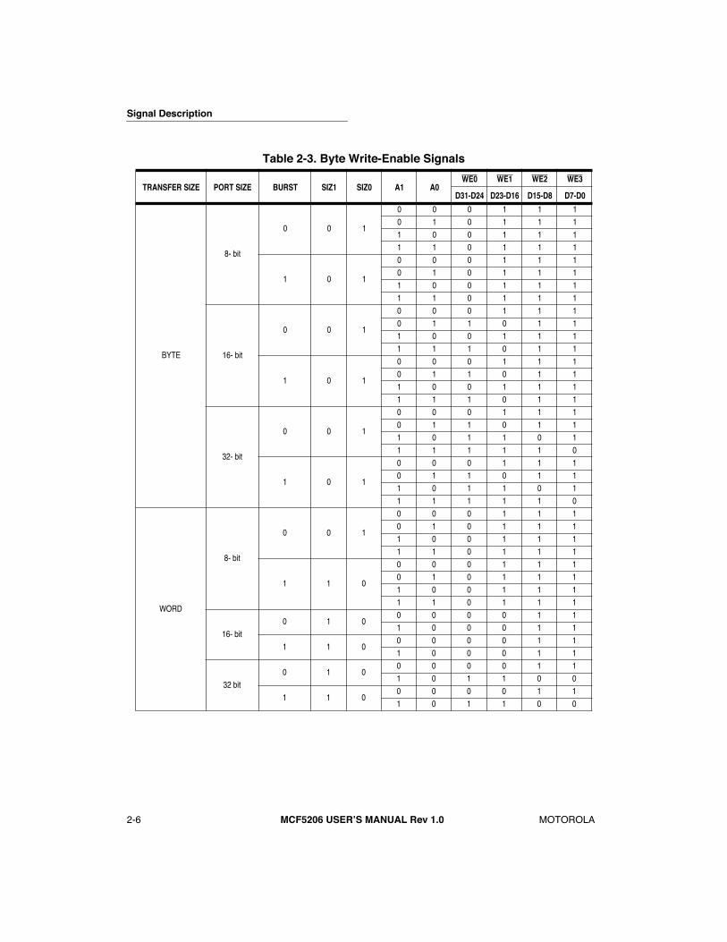
Signal Description
2-6
MCF5206 USERÕS MANUAL Rev 1.0
MOTOROLA
Table 2-3. Byte Write-Enable Signals
TRANSFER SIZE PORT SIZE BURST SIZ1 SIZ0 A1 A0WE0 WE1 WE2 WE3
D31-D24 D23-D16 D15-D8 D7-D0
BYTE
8- bit
0 0 1
0 0 0 1 1 10 1 0 1 1 11 0 0 1 1 11 1 0 1 1 1
1 0 1
0 0 0 1 1 10 1 0 1 1 11 0 0 1 1 11 1 0 1 1 1
16- bit
0 0 1
0 0 0 1 1 10 1 1 0 1 11 0 0 1 1 11 1 1 0 1 1
1 0 1
0 0 0 1 1 10 1 1 0 1 11 0 0 1 1 11 1 1 0 1 1
32- bit
0 0 1
0 0 0 1 1 10 1 1 0 1 11 0 1 1 0 11 1 1 1 1 0
1 0 1
0 0 0 1 1 10 1 1 0 1 11 0 1 1 0 11 1 1 1 1 0
WORD
8- bit
0 0 1
0 0 0 1 1 10 1 0 1 1 11 0 0 1 1 11 1 0 1 1 1
1 1 0
0 0 0 1 1 10 1 0 1 1 11 0 0 1 1 11 1 0 1 1 1
16- bit0 1 0
0 0 0 0 1 11 0 0 0 1 1
1 1 00 0 0 0 1 11 0 0 0 1 1
32 bit0 1 0
0 0 0 0 1 11 0 1 1 0 0
1 1 00 0 0 0 1 11 0 1 1 0 0

Signal Description
MOTOROLA
MCF5206 USERÕS MANUAL Rev 1.0
2-7
2.4.1 Interrupt Priority Level/ Interrupt Request (IPL[2]/IRQ[7],IPL[1]/IRQ[4], IPL[0]/IRQ[1])
You can program these three active-low input pins as either interrupt priority-level signals (IPL[2:0]) or predefined interrupt request pins (IRQ[7], IRQ[4], IRQ[1]). Programming the Pin Assignment Register (PAR) in the SIM determines the function of these pins. During reset, these pins are configured to be predefined interrupt requests.
When these pins are programmed to be interrupt priority-level signals, IPL[2:0] signals the priority level (7-1) of an external interrupt; IPL[2:0]=000 (level 7) indicates the highest unmaskable interrupt, while IPL[2:0]=111 (level 0) indicates no interrupt request. When these pins are programmed to be interrupt-request signals, the assertion of IRQ[7] generates a level 7 interrupt, IRQ[4] generates a level 4 interrupt, and IRQ[1] generates a level 1 interrupt.
LONGWORD
8-bit
0 0 1
0 0 0 1 1 10 1 0 1 1 11 0 0 1 1 11 1 0 1 1 1
1 0 0
0 0 0 1 1 10 1 0 1 1 11 0 0 1 1 11 1 0 1 1 1
16-bit0 1 0
0 0 0 0 1 11 0 0 0 1 1
1 0 00 0 0 0 1 11 0 0 0 1 1
32-bit0 0 0 0 0 0 0 0 01 0 0 0 0 0 0 0 0
LINE
8-bit
0 0 1
0 0 0 1 1 10 1 0 1 1 11 0 0 1 1 11 1 0 1 1 1
1 1 1
0 0 0 1 1 10 1 0 1 1 11 0 0 1 1 11 1 0 1 1 1
16-bit0 1 0
0 0 0 0 1 11 0 0 0 1 1
1 1 10 0 0 0 1 11 0 0 0 1 1
32-Bit0 0 0 0 0 0 0 0 01 1 1 0 0 0 0 0 0
Table 2-3. Byte Write-Enable Signals (Continued)
TRANSFER SIZE PORT SIZE BURST SIZ1 SIZ0 A1 A0WE0 WE1 WE2 WE3
D31-D24 D23-D16 D15-D8 D7-D0
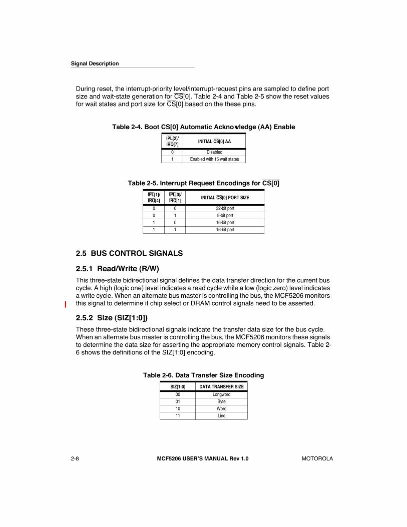
Signal Description
2-8
MCF5206 USERÕS MANUAL Rev 1.0
MOTOROLA
During reset, the interrupt-priority level/interrupt-request pins are sampled to define port size and wait-state generation for CS[0]. Table 2-4 and Table 2-5 show the reset values for wait states and port size for CS[0] based on the these pins.
2.5 BUS CONTROL SIGNALS
2.5.1 Read/Write (R/W)
This three-state bidirectional signal defines the data transfer direction for the current bus cycle. A high (logic one) level indicates a read cycle while a low (logic zero) level indicates a write cycle. When an alternate bus master is controlling the bus, the MCF5206 monitors this signal to determine if chip select or DRAM control signals need to be asserted.
2.5.2 Size (SIZ[1:0])
These three-state bidirectional signals indicate the transfer data size for the bus cycle. When an alternate bus master is controlling the bus, the MCF5206 monitors these signals to determine the data size for asserting the appropriate memory control signals. Table 2-6 shows the definitions of the SIZ[1:0] encoding.
Table 2-4. Boot CS[0] Automatic Acknowledge (AA) Enable
IPL[2]/IRQ[7]
INITIAL CS[0] AA
0 Disabled1 Enabled with 15 wait states
Table 2-5. Interrupt Request Encodings for CS[0]
IPL[1]/IRQ[4]
IPL[0]/IRQ[1]
INITIAL CS[0] PORT SIZE
0 0 32-bit port0 1 8-bit port1 0 16-bit port1 1 16-bit port
Table 2-6. Data Transfer Size Encoding
SIZ[1:0] DATA TRANSFER SIZE
00 Longword 01 Byte10 Word11 Line
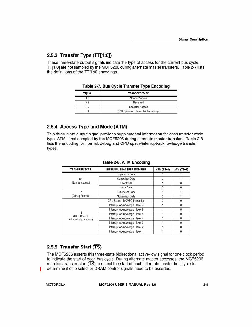
Signal Description
MOTOROLA
MCF5206 USERÕS MANUAL Rev 1.0
2-9
2.5.3 Transfer Type (TT[1:0])
These three-state output signals indicate the type of access for the current bus cycle. TT[1:0] are not sampled by the MCF5206 during alternate master transfers. Table 2-7 lists the definitions of the TT[1:0] encodings.
2.5.4 Access Type and Mode (ATM)
This three-state output signal provides supplemental information for each transfer cycle type. ATM is not sampled by the MCF5206 during alternate master transfers. Table 2-8 lists the encoding for normal, debug and CPU space/interrupt-acknowledge transfer types.
2.5.5 Transfer Start (TS)
The MCF5206 asserts this three-state bidirectional active-low signal for one clock period to indicate the start of each bus cycle. During alternate master accesses, the MCF5206 monitors transfer start (TS) to detect the start of each alternate master bus cycle to determine if chip select or DRAM control signals need to be asserted.
Table 2-7. Bus Cycle Transfer Type Encoding
TT[1:0] TRANSFER TYPE
0 0 Normal Access0 1 Reserved1 0 Emulator Access1 1 CPU Space or Interrupt Acknowledge
Table 2-8. ATM Encoding
TRANSFER TYPE INTERNAL TRANSFER MODIFIER ATM (TS=0) ATM (TS=1)
00(Normal Access)
Supervisor Code 1 1Supervisor Data 0 1
User Code 1 0User Data 0 0
10(Debug Access)
Supervisor Code 1 1Supervisor Data 0 1
11(CPU Space/
Acknowledge Access)
CPU Space - MOVEC Instruction 0 0Interrupt Acknowledge - level 7 1 0Interrupt Acknowledge - level 6 1 0Interrupt Acknowledge - level 5 1 0Interrupt Acknowledge - level 4 1 0Interrupt Acknowledge - level 3 1 0Interrupt Acknowledge - level 2 1 0Interrupt Acknowledge - level 1 1 0
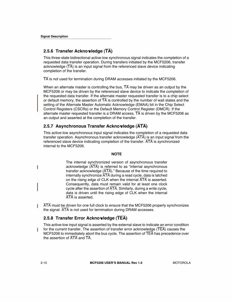
Signal Description
2-10
MCF5206 USERÕS MANUAL Rev 1.0
MOTOROLA
2.5.6 Transfer Acknowledge (TA)
This three-state bidirectional active-low synchronous signal indicates the completion of a requested data transfer operation. During transfers initiated by the MCF5206, transfer acknowledge (TA) is an input signal from the referenced slave device indicating completion of the transfer.
TA is not used for termination during DRAM accesses initiated by the MCF5206.
When an alternate master is controlling the bus, TA may be driven as an output by the MCF5206 or may be driven by the referenced slave device to indicate the completion of the requested data transfer. If the alternate master requested transfer is to a chip select or default memory, the assertion of TA is controlled by the number of wait states and the setting of the Alternate Master Automatic Acknowledge (EMAA) bit in the Chip Select Control Registers (CSCRs) or the Default Memory Control Register (DMCR). If the alternate master requested transfer is a DRAM access, TA is driven by the MCF5206 as an output and asserted at the completion of the transfer.
2.5.7 Asynchronous Transfer Acknowledge (ATA)
This active-low asynchronous input signal indicates the completion of a requested data transfer operation. Asynchronous transfer acknowledge (ATA) is an input signal from the referenced slave device indicating completion of the transfer. ATA is synchronized internal to the MCF5206.
NOTE
The internal synchronized version of asynchronous transferacknowledge (ATA) is referred to as Òinternal asynchronoustransfer acknowledge (ATA).Ó Because of the time required tointernally synchronize ATA during a read cycle, data is latchedon the rising edge of CLK when the internal ATA is asserted.Consequently, data must remain valid for at least one clockcycle after the assertion of ATA. Similarly, during a write cycle,data is driven until the rising edge of CLK when the internalATA is asserted.
ATA must be driven for one full clock to ensure that the MCF5206 properly synchronizes the signal. ATA is not used for termination during DRAM accesses.
2.5.8 Transfer Error Acknowledge (TEA)
This active-low input signal is asserted by the external slave to indicate an error condition for the current transfer. The assertion of transfer error acknowledge (TEA) causes the MCF5206 to immediately abort the bus cycle. The assertion of TEA has precedence over the assertion of ATA and TA.

Signal Description
MOTOROLA
MCF5206 USERÕS MANUAL Rev 1.0
2-11
NOTE
TEA can be asserted to a maximum of one clock after theassertion of ATA and still be recognized.
TEA has no effect during DRAM accesses.
2.6 BUS ARBITRATION SIGNALS
2.6.1 Bus Request (BR)
This active-low output signal indicates to an external arbiter that the MCF5206 needs use of the bus for one or more bus cycles. BR is negated when the MCF5206 begins an access to the external bus, and remains negated until another internal request occurs with BG negated.
2.6.2 Bus Grant (BG)
An external arbiter asserts this active-low input signal to indicate that the MCF5206 can become master of the external bus at the next rising edge of CLK. When the arbiter negates BG, the MCF5206 relinquishes the bus as soon as the current transfer is complete, provided the bus lock bit in the SIMR is not set. If the bus lock bit is set, the MCF5206 retains bus mastership until the bus lock bit is cleared. The external arbiter must not grant the bus to any other master until the MCF5206 negates BD.
2.6.3 Bus Driven (BD)
The MCF5206 asserts this active-low output signal to indicate it has assumed explicit mastership of the external bus. The MCF5206 asserts BD if BG is asserted and either the MCF5206 has a pending bus transfer or the bus lock bit in the SIMR is set to 1. If the MCF5206 is granted mastership of the external bus, but does not have a pending bus transfer and the bus lock bit in the SIMR is cleared, the BD signal is not asserted (implicit mastership of the bus is assumed).
If BG is negated to the MCF5206 during a bus transfer and the bus lock bit in the SIMR is cleared, the MCF5206 completes the last transfer of the current access, negates BD, and three-states all bus signals on the rising edge of CLK. If the MCF5206 loses bus ownership during an idle bus period with BD asserted and the bus lock bit in the SIMR cleared, the MCF5206 negates BD and three-states all bus signals on the next rising edge of CLK. If the MCF5206 loses bus ownership during an idle bus period with BD asserted and the bus lock bit in the SIMR set to 1, the MCF5206 continues to assert BD and maintains explicit ownership of the external bus until the bus lock bit in the SIMR is cleared.
Signal Description
2-12
MCF5206 USERÕS MANUAL Rev 1.0
MOTOROLA
2.7 CLOCK AND RESET SIGNALS
2.7.1 Clock Input (CLK)
CLK is the MCF5206 synchronous clock, and clocks or sequences the MCF5206 internal logic and external signals.
2.7.2 Reset (RSTI)
Asserting the active-low RSTI input causes the MCF5206 processor to enter reset exception processing. When RSTI is recognized, the address bus, data bus, TT, SIZ, R/W, ATM and TS is three-stated; BR and BD is negated.
If RSTI is asserted with HIZ asserted, the MCF5206 enters master reset mode. In this reset mode, the entire MCF5206 (including the DRAM controller refresh circuitry) is reset. You must use master reset for all power-on resets.
If RSTI is asserted with HIZ negated, the MCF5206 enters normal reset mode. In this reset mode, the DRAM controller refresh circuitry is not reset and continues to generate refresh cycles at the programmed rate and with the programmed waveform timing.
2.7.3 Reset Out (RTS[2]/RSTO)
RTS[2] is multiplexed with the RSTO signal. Programming the Pin Assignment Register (PAR) in the SIM determines the function of this pin. During reset, this pin is configured to be RSTO.
RSTO is an output that drives peripherals to reset. There are no more than two clocks from the assertion of RSTI to the assertion of RSTO, and RSTO remains asserted for at least 31 clocks after the negation of RSTI. RSTO is also asserted for at least 31 clocks on a software watchdog time-out that is programmed to generate a reset.
2.8 DRAM CONTROLLER SIGNALS
The following DRAM signals provide a glueless interface to external DRAM:
2.8.1 Row Address Strobes (RAS[1:0])
These active-low output signals provide control for the row address strobe (RAS) input pins on industry-standard DRAMs. There is one RAS output for each DRAM bank: RAS[0] controls DRAM bank 0 and RAS[1] controls DRAM bank 1. You can customize RAS timing to match the specifications of the DRAM being used by programming the DRAMC Timing Register (see
Section 10.4.2.2 DRAM Controller Timing register (DCTR).
)
.
2.8.2 Column Address Strobes (CAS[3:0])
These active-low output signals provide control for the column address strobe (CAS) input pins on industry-standard DRAMs. The CAS signals enable data byte lanes: CAS[0] controls access to D[31:24], CAS[1] to D[23:16], CAS[2] to D[15:8], and CAS[3] to D[7:0]. You should use CAS[3:0] for a 32-bit wide DRAM bank, CAS[1:0] for a 16-bit wide DRAM
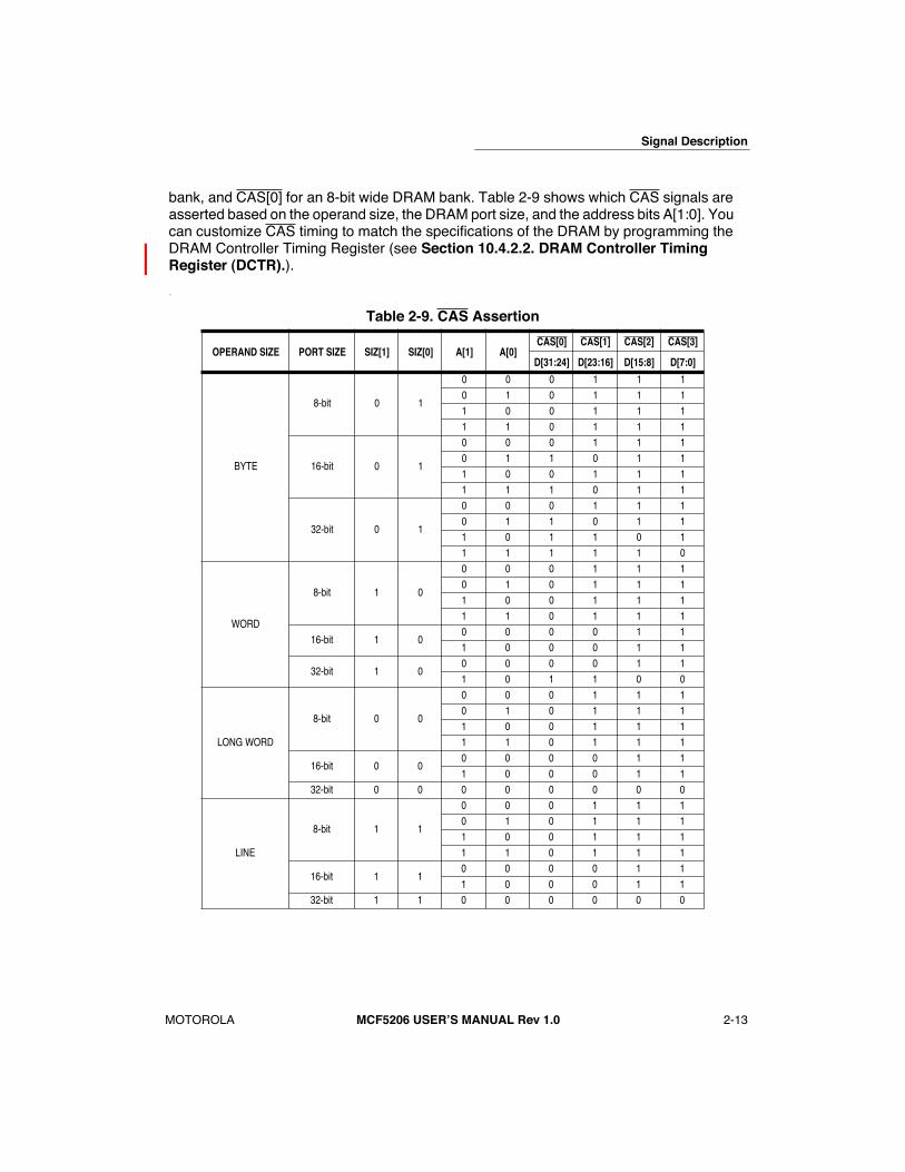
Signal Description
MOTOROLA
MCF5206 USERÕS MANUAL Rev 1.0
2-13
bank, and CAS[0] for an 8-bit wide DRAM bank. Table 2-9 shows which CAS signals are asserted based on the operand size, the DRAM port size, and the address bits A[1:0]. You can customize CAS timing to match the specifications of the DRAM by programming the DRAM Controller Timing Register (see
Section 10.4.2.2. DRAM Controller Timing Register (DCTR).
).
.
Table 2-9. CAS Assertion
OPERAND SIZE PORT SIZE SIZ[1] SIZ[0] A[1] A[0]CAS[0] CAS[1] CAS[2] CAS[3]
D[31:24] D[23:16] D[15:8] D[7:0]
BYTE
8-bit 0 1
0 0 0 1 1 10 1 0 1 1 11 0 0 1 1 11 1 0 1 1 1
16-bit 0 1
0 0 0 1 1 10 1 1 0 1 11 0 0 1 1 11 1 1 0 1 1
32-bit 0 1
0 0 0 1 1 10 1 1 0 1 11 0 1 1 0 11 1 1 1 1 0
WORD
8-bit 1 0
0 0 0 1 1 10 1 0 1 1 11 0 0 1 1 11 1 0 1 1 1
16-bit 1 00 0 0 0 1 11 0 0 0 1 1
32-bit 1 00 0 0 0 1 11 0 1 1 0 0
LONG WORD
8-bit 0 0
0 0 0 1 1 10 1 0 1 1 11 0 0 1 1 11 1 0 1 1 1
16-bit 0 00 0 0 0 1 11 0 0 0 1 1
32-bit 0 0 0 0 0 0 0 0
LINE
8-bit 1 1
0 0 0 1 1 10 1 0 1 1 11 0 0 1 1 11 1 0 1 1 1
16-bit 1 10 0 0 0 1 11 0 0 0 1 1
32-bit 1 1 0 0 0 0 0 0

Signal Description
2-14
MCF5206 USERÕS MANUAL Rev 1.0
MOTOROLA
2.8.3 DRAM Write (DRAMW)
This active-low output signal is asserted during DRAM write cycles and negated during DRAM read cycles. The DRAMW signal is negated during refresh cycles and is provided (in addition to the R/W signal) to allow refreshes to occur during non-DRAM cycles (regardless of the state of the R/W signal). The R/W signal indicates the direction of all bus transfers, while DRAMW is valid only during DRAM transfers.
2.9 UART MODULE SIGNALS
The signals listed below transfer serial data between the two UART modules (UART1 and UART2) and external peripherals.
2.9.1 Receive Data (RxD[1], RxD[2])
These are the inputs on which serial data is received by the UART modules. RxD[1] corresponds to UART1 and RxD[2] corresponds to UART2. Data is sampled on RxD[1] and RxD[2] on the rising edge of the serial clock source, with the least significant bit received first.
2.9.2 Transmit Data (TxD[1], TxD[2])
The UART modules transmit serial data on these outputs. TxD[1] corresponds to UART1 and TxD[2] corresponds to UART2. Data is transmitted on the falling edge of the serial clock source, with the least significant bit (LSB) transmitted first. When no data is being transmitted or the transmitter is disabled, these two signals are held high. TxD[1] and TxD[2] are also held high in local loopback mode.
2.9.3 Request To Send (RTS[1], RTS[2]/RSTO)
RTS[2] is multiplexed with the RSTO signal. Programming the Pin Assignment Register (PAR) in the SIM determines the function of this pin. During reset, this pin is configured to be RSTO.
The request-to-send output indicates to the peripheral device that the UART module is ready to receive data. RTS[1] corresponds to UART1 and RTS[2] corresponds to UART2.
2.9.4 Clear To Send (CTS[1], CTS[2])
Peripherals drive these inputs to indicate to the UART module that it can begin data transmission. CTS[1] corresponds to UART1 and CTS[2] corresponds to UART2.
2.10 TIMER MODULE SIGNALS
The signal descriptions that follow are the external interface to the two general purpose timer modules (Timer1 and Timer2).

Signal Description
MOTOROLA
MCF5206 USERÕS MANUAL Rev 1.0
2-15
2.10.1 Timer Input (TIN[2], TIN[1])
You can program the timer input to be the clock for the timer module. You can also program the timer module to trigger a capture on the rising edge, falling edge, or both edges of the timer input. TIN[1] corresponds to Timer1 and TIN[2] corresponds to Timer2.
2.10.2 Timer Output (TOUT[2], TOUT[1])
The programmable timer output pulses or toggles when the timer reaches the programmed count value. TOUT[1] corresponds to Timer1 and TOUT[2] corresponds to Timer2.
2.11 M-BUS MODULE SIGNALS
The M-Bus module acts as quick two-wire, bidirectional serial interface between the MCF5206 and peripherals with an M-Bus interface (e.g., LED controller, A-to-D converter, D-to-A converter). All devices connected to the M-Bus must have open-drain or open-collector outputs.
2.11.1 M-Bus Serial Clock (SCL)
This bidirectional, open-drain signal is the clock signal for M-Bus module operation. It is controlled by the M-Bus module when the bus is in master mode; all M-Bus devices drive this signal to synchronize M-Bus timing.
2.11.2 M-Bus Serial Data (SDA)
This bidirectional, open-drain signal is the data input/output for the serial M-Bus interface.
2.12 GENERAL PURPOSE I/O SIGNALS
2.12.1 General-Purpose I/O (PP[7:4]/PST[3:0])
These general purpose I/O signals are multiplexed with the processor status signals, PST[3:0]. Programming the Pin Assignment Register (PAR) in the SIM determines the function of these pins. During reset, these pins are configured as general purpose inputs.
When programmed as general purpose I/O, you can configure these signals as inputs or outputs and they can be asserted and negated through programmable control.
2.12.2 Parallel Port (General-Purpose I/O) (PP[3:0]/DDATA[3:0])
These programmable parallel port signals are multiplexed with the debug data signals, DDATA[3:0]. Programming the Pin Assignment Register (PAR) in the SIM determines the function of these pins. During reset, these pins are configured as general purpose inputs.
When programmed as general purpose I/O, you can configure these signals as inputs or outputs and they can be asserted and negated through programmable control.
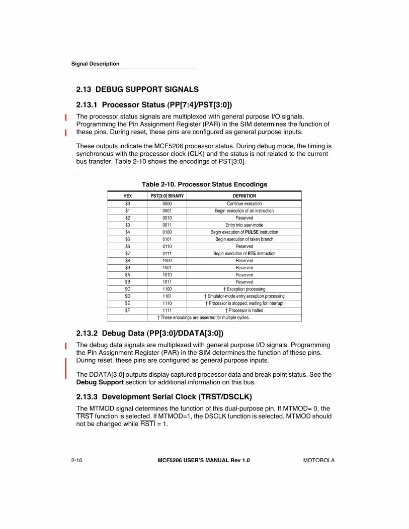
Signal Description
2-16 MCF5206 USERÕS MANUAL Rev 1.0 MOTOROLA
2.13 DEBUG SUPPORT SIGNALS
2.13.1 Processor Status (PP[7:4]/PST[3:0])The processor status signals are multiplexed with general purpose I/O signals. Programming the Pin Assignment Register (PAR) in the SIM determines the function of these pins. During reset, these pins are configured as general purpose inputs.
These outputs indicate the MCF5206 processor status. During debug mode, the timing is synchronous with the processor clock (CLK) and the status is not related to the current bus transfer. Table 2-10 shows the encodings of PST[3:0].
.
2.13.2 Debug Data (PP[3:0]/DDATA[3:0])The debug data signals are multiplexed with general purpose I/O signals. Programming the Pin Assignment Register (PAR) in the SIM determines the function of these pins. During reset, these pins are configured as general purpose inputs.
The DDATA[3:0] outputs display captured processor data and break point status. See the Debug Support section for additional information on this bus.
2.13.3 Development Serial Clock (TRST/DSCLK)The MTMOD signal determines the function of this dual-purpose pin. If MTMOD= 0, the TRST function is selected. If MTMOD=1, the DSCLK function is selected. MTMOD should not be changed while RSTI = 1.
Table 2-10. Processor Status Encodings
HEX PST[3:0] BINARY DEFINITION
$0 0000 Continue execution$1 0001 Begin execution of an instruction$2 0010 Reserved$3 0011 Entry into user-mode$4 0100 Begin execution of PULSE instruction$5 0101 Begin execution of taken branch$6 0110 Reserved$7 0111 Begin execution of RTE instruction$8 1000 Reserved$9 1001 Reserved$A 1010 Reserved$B 1011 Reserved$C 1100 Exception processing$D 1101 Emulator-mode entry exception processing$E 1110 Processor is stopped, waiting for interrupt$F 1111 Processor is halted
These encodings are asserted for multiple cycles.
Signal Description
MOTOROLA MCF5206 USERÕS MANUAL Rev 1.0 2-17
The DSCLK input signal is used as the development serial clock for the serial interface to the debug module.The maximum frequency for the DSCLK signal is 1/2 the CLK frequency. See the Debug Support section for additional information on this signal.
2.13.4 Break Point (TMS/BKPT)The MTMOD signal determines the function of this dual-purpose pin. If MTMOD = 0, then the TMS function is selected. If MTMOD =1, the BKPT function is selected. MTMOD should not change while RSTI = 1.
The assertion of the active-low BKPT input signal causes a hardware breakpoint to occur in the processor when in the debug mode. See the Debug Support section for additional information on this signal.
2.13.5 Development Serial Input (TDI/DSI)The MTMOD signal determines the function of this dual-purpose pin. If MTMOD = 0, then TDI is selected. If MTMOD = 1, then DSI is selected. MTMOD should not change while RSTI = 1.
The DSI input signal is the serial data input for the Debug module commands. See the Debug Support section for additional information on this signal.
2.13.6 Development Serial Output (TDO/DSO)The MTMOD signal determines the function of this dual-purpose pin. When MTMOD = 0, TDO is selected. When MTMOD = 1, then DSO is selected. MTMOD should not change while RSTI = 1.
The DSO output signal is the serial data output for the debug module responses. See the Debug Support section for additional information on this signal.
2.14 JTAG SIGNALS
2.14.1 Test Clock (TCK)TCK is the dedicated JTAG test logic clock that is independent of the MCF5206 processor clock. The internal JTAG controller logic is designed such that holding TCK high or low for an indefinite period of time does not cause the JTAG test logic to lose state information. TCK should be grounded if it is not used.
2.14.2 Test Reset (TRST/DSCLK)The MTMOD signal determines the function of this dual-purpose pin. If MTMOD= 0, the TRST function is selected. If MTMOD=1, the DSCLK function is selected. MTMOD should not be changed while RSTI = 1.
The assertion of the active-low TRST input pin asynchronously resets the JTAG TAP controller to the test logic reset state, causing the JTAG instruction register to choose the
Signal Description
2-18 MCF5206 USERÕS MANUAL Rev 1.0 MOTOROLA
ÔÔbypassÕÕ command. When this occurs, all the JTAG logic is benign and does not interfere with the normal functionality of the MCF5206 processor. Although this signal is asynchronous, we recommend that TRST make only a 0 to 1 (asserted to negated) transition while TMS is held at a logic 1 value. TRST has an internal pullup so that if it is not driven low, its value defaults to a logic level of 1. However, if JTAG is not being used, TRST can either be tied to ground, placing the JTAG controller in the test logic reset state immediately, or tied to VDD, causing the JTAG controller (if TMS is a logic 1) to eventually end up in the test logic reset state after five clocks of TCK.
2.14.3 Test Mode Select (TMS/BKPT)The MTMOD signal determines the function of this dual-purpose pin. If MTMOD = 0, then the TMS function is selected. If MTMOD =1, the BKPT function is selected. MTMOD should not change while RSTI = 1.
The TMS input signal provides the JTAG controller with information to determine which test operation should be performed. The value of TMS and the current state of the internal 16-state JTAG controller state machine at the rising edge of TCK determine whether the JTAG controller holds its current state or advances to the next state. This directly controls whether JTAG data or instruction operations occur. TMS has an internal pullup so that if it is not driven low, its value defaults to a logic level of 1. However, if TMS is not being used, it should be tied to VDD.
2.14.4 Test Data Input (TDI/DSI)The MTMOD signal determines the function of this dual-purpose pin. If MTMOD = 0, then TDI is selected. If MTMOD = 1, then DSI is selected. MTMOD should not change while RSTI = 1.
The TDI input signal provides the serial data port for loading the various JTAG shift registers (the boundary scan register, the bypass register, and the instruction register). Shifting in of data depends on the state of the JTAG controller state machine and the instruction currently in the instruction register. This data shift occurs on the rising edge of TCK. TDI also has an internal pullup so that if it is not driven low, its value defaults to a logic level of 1. However, if TDI is not being used, it should be tied to VDD.
2.14.5 Test Data Output (TDO/DSO)The MTMOD signal determines the function of this dual-purpose pin. When MTMOD = 0, TDO is selected. When MTMOD = 1, then DSO is selected. MTMOD should not change while RSTI = 1.
The TDO output signal provides the serial data port for outputting data from the JTAG logic. Shifting out of data depends on the state of the JTAG controller state machine and the instruction currently in the instruction register. This data shift occurs on the falling edge of TCK. When TDO is not outputting test data, it is placed in a high-impedence state. TDO can also be three-stated to allow bussed or parallel connections to other devices having JTAG.
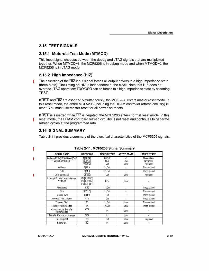
Signal Description
MOTOROLA MCF5206 USERÕS MANUAL Rev 1.0 2-19
2.15 TEST SIGNALS
2.15.1 Motorola Test Mode (MTMOD)This input signal chooses between the debug and JTAG signals that are multiplexed together. When MTMOD=1, the MCF5206 is in debug mode and when MTMOD=0, the MCF5206 is in JTAG mode.
2.15.2 High Impedance (HIZ)The assertion of the HIZ input signal forces all output drivers to a high-impedance state (three-state). The timing on HIZ is independent of the clock. Note that HIZ does not override JTAG operation; TDO/DSO can be forced to a high-impedance state by asserting TRST.
If RSTI and HIZ are asserted simultaneously, the MCF5206 enters master reset mode. In this reset mode, the entire MCF5206 (including the DRAM controller refresh circuitry) is reset. You must use master reset for all power-on resets.
If RSTI is asserted while HIZ is negated, the MCF5206 enters normal reset mode. In this reset mode, the DRAM controller refresh circuitry is not reset and continues to generate refresh cycles at the programmed rate.
2.16 SIGNAL SUMMARYTable 2-11 provides a summary of the electrical characteristics of the MCF5206 signals.
Table 2-11. MCF5206 Signal Summary
SIGNAL NAME MNEMONIC INPUT/OUTPUT ACTIVE STATE RESET STATE
Address[27:24]/Chip Select[7:4]/Write Enable[0:3]
A[27:24]/CS[7:4]/WE[0:3]
In,Out/Out/Out
-/Low/Low
Three-state/Negated/Negated
Address A[23:0] In,Out - Three-statedData D[31:0] In,Out - Three-stated
Chip Select3:0] CS[3:0] Out Low NegatedInterrupt Priority Level/ Interrupt
RequestIPL[2]/IRQ[7]IPL[1]/IRQ[4]IPL[0]/IRQ[1]
In/In Low -
Read/Write R/W In,Out - Three-statedSize SIZ[1:0] In,Out - Three-stated
Transfer Type TT[1:0] Out - Three-statedAccess Type & Mode ATM Out - Three-stated
Transfer Start TS In,Out Low Three-statedTransfer Acknowledge TA In,Out Low Three-statedAsynchronous Transfer
Acknowledge ATA In Low -
Transfer Error Acknowledge TEA In Low -Bus Request BR Out Low Negated
Bus Grant BG In Low -
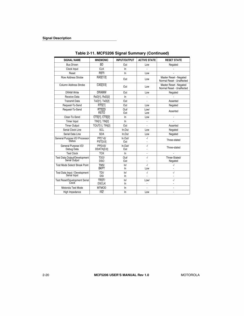
Signal Description
2-20 MCF5206 USERÕS MANUAL Rev 1.0 MOTOROLA
Bus Driven BD Out Low NegatedClock Input CLK In - -
Reset RSTI In Low -Row Address Strobe RAS[1:0] Out Low Master Reset - Negated
Normal Reset - UnaffectedColumn Address Strobe CAS[3:0] Out Low Master Reset - Negated
Normal Reset - UnaffectedDRAM Write DRAMW Out Low NegatedReceive Data RxD[1], RxD[2] In - -Transmit Data TxD[1], TxD[2] Out - Asserted
Request-To-Send RTS[1] Out Low NegatedRequest-To-Send RTS[2]/
RSTOOut/Out
Low/Low Asserted
Clear-To-Send CTS[1], CTS[2] In Low -Timer Input TIN[1], TIN[2] In - -
Timer Output TOUT[1], TIN[2] Out - AssertedSerial Clock Line SCL In,Out Low NegatedSerial Data Line SDA In,Out Low Negated
General Purpose I/O/ Processor Status
PP[7:4]/PST[3:0]
In.Out/Out
-/- Three-stated
General Purpose I/O/ Debug Data
PP[3:0]/DDATA[3:0]
In,Out/Out
-/- Three-stated
Test Clock TCK In - -Test Data Output/Development
Serial OutputTDO/DSO
Out/Out
-/-
Three-Stated/Negated
Test Mode Select/ Break Point TMS/BKPT
In/In
-/Low
-/-
Test Data Input / Development Serial Input
TDI/DSI
In/In
-/-
-/-
Test Reset/Development Serial Clock
TRST/DSCLK
In/In
Low/-
-/-
Motorola Test Mode MTMOD In - -High Impedance HIZ In Low -
Table 2-11. MCF5206 Signal Summary (Continued)
SIGNAL NAME MNEMONIC INPUT/OUTPUT ACTIVE STATE RESET STATE
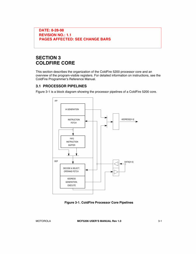
MOTOROLA
MCF5206 USERÕS MANUAL Rev 1.0
3-1
2
3
4
5
6
7
8
9
10
11
12
13
14
15
16
1
3SECTION 3COLDFIRE CORE
This section describes the organization of the ColdFire 5200 processor core and an overview of the program-visible registers. For detailed information on instructions, see the
ColdFire ProgrammerÕs Reference Manual
.
3.1 PROCESSOR PIPELINES
Figure 3-1 is a block diagram showing the processor pipelines of a ColdFire 5200 core.
Figure 3-1. ColdFire Processor Core Pipelines
IA GENERATION
INSTRUCTION
FETCH
FIFO
INSTRUCTION
BUFFER
DECODE & SELECT,
OPERAND FETCH
ADDRESS
GENERATION,
EXECUTE
IFP
OEP
ADDRESS[31:0]
DATA[31:0]
DATE: 8-28-98REVISION NO.: 1.1PAGES AFFECTED: SEE CHANGE BARS
ColdFire Core
3-2
MCF5206 USERÕS MANUAL Rev 1.0
MOTOROLA
2
3
4
5
6
7
8
9
10
12
13
14
15
16
1
The processor core is comprised of two separate pipelines that are decoupled by an instruction buffer. The Instruction Fetch Pipeline (IFP) is responsible for instruction address generation and instruction fetch. The instruction buffer is a first-in-first-out (FIFO) buffer that holds prefetched instructions awaiting execution in the Operand Execution Pipeline (OEP). The OEP includes two pipeline stages. The first stage decodes instructions and selects operands (DSOC); the second stage (AGEX) performs instruction execution and calculates operand effective addresses, if needed.
3.2 PROCESSOR REGISTER DESCRIPTION
The following paragraphs describe the processor registers in the user and supervisor programming models. The appropriate programming model is selected based on the privilege level (user mode or supervisor mode) of the processor as defined by the S-bit of the status register.
3.2.1 User Programming Model
Figure 3-2 illustrates the user programming model. The model is the same as for M68000 Family microprocessors, consisting of the following registers:
¥ 16 general-purpose 32-bit registers (D0ÐD7, A0ÐA7)
¥ 32-bit program counter (PC)
¥ 8-bit condition code register (CCR)
3.2.1.1 DATA REGISTERS (D0ÐD7).
Registers D0ÐD7 are used as data registers for bit (1 bit), byte (8-bit), word (16-bit) and longword (32-bit) operations and can also be used as index registers.
3.2.1.2 ADDRESS REGISTERS (A0ÐA6).
These registers can be used as software stack pointers, index registers, or base address registers as well as for word and longword operations.
3.2.1.3 STACK POINTER (A7).
ColdFire supports a single hardware stack pointer (A7) for explicit references or implicit ones during stacking for subroutine calls and returns and exception handling. The initial value of A7 is loaded from the reset exception vector, address $0. The same register is used for both user and supervisor mode as well as word and longword operations.
A subroutine call saves the PC on the stack and the return restores it from the stack. Both the PC and the SR are saved on the stack during the processing of exceptions and interrupts. The return from exception instruction restores the SR and PC values from the stack.
3.2.1.4 PROGRAM COUNTER.
The PC contains the address of the currently executing instruction. During instruction execution and exception processing, the processor automatically increments the contents of the PC or places a new value in the PC, as appropriate. For some addressing modes, the PC can be used as a pointer for PC-relative operand addressing.

ColdFire Core
MOTOROLA
MCF5206 USERÕS MANUAL Rev 1.0
3-3
2
3
5
6
7
8
9
11
12
13
15
16
1
2
3
1
3.2.1.5 CONDITION CODE REGISTER .
The CCR is the least significant byte of the processor status register (SR). Bits 4Ð0 represent indicator flags based on results generated by processor operations. Bit 4, the extend bit (X-bit), is also used as an input operand during multiprecision arithmetic computations.
XÑ extend condition code bit
NÐ negative condition code bitSet if the most significant bit of the result is set; otherwise cleared
ZÐ zero condition code bitSet if the result equals zero; otherwise cleared
VÐ overflow condition code bitSet if an arithmetic overflow occurs implying that the result cannot be represented in the operand size; otherwise cleared
CÐ carry condition code bitSet if a carryout of the operand MSB occurs for an addition, or if a borrow occurs in a subtraction; otherwise cleared
Set to the value of the C-bit for arithmetic operations; otherwise not affected.
Figure 3-2. User Programming Model
4 3 2 1 0X N Z V C
D0D1D2D3D4D5D6D7
A0A1A2A3A4A5A6
A7
CCR
PC
15 7 0
15 031
DATAREGISTERS
ADDRESSREGISTERS
STACKPOINTER
PROGRAMCOUNTER
CONDITIONCODEREGISTER
7
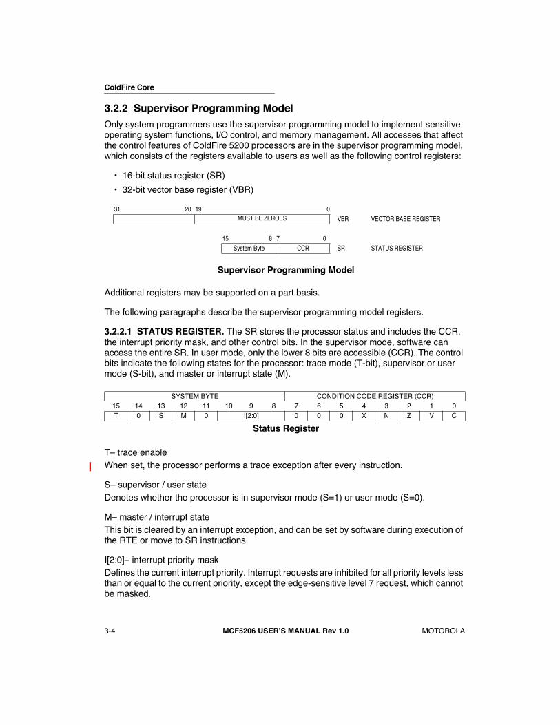
ColdFire Core
3-4
MCF5206 USERÕS MANUAL Rev 1.0
MOTOROLA
2
3
4
5
6
7
8
9
10
12
13
14
15
16
1
3.2.2 Supervisor Programming Model
Only system programmers use the supervisor programming model to implement sensitive operating system functions, I/O control, and memory management. All accesses that affect the control features of ColdFire 5200 processors are in the supervisor programming model, which consists of the registers available to users as well as the following control registers:
¥ 16-bit status register (SR)
¥ 32-bit vector base register (VBR)
Supervisor Programming Model
Additional registers may be supported on a part basis.
The following paragraphs describe the supervisor programming model registers.
3.2.2.1 STATUS REGISTER.
The SR stores the processor status and includes the CCR, the interrupt priority mask, and other control bits. In the supervisor mode, software can access the entire SR. In user mode, only the lower 8 bits are accessible (CCR). The control bits indicate the following states for the processor: trace mode (T-bit), supervisor or user mode (S-bit), and master or interrupt state (M).
TÐ trace enableWhen set, the processor performs a trace exception after every instruction.
SÐ supervisor / user stateDenotes whether the processor is in supervisor mode (S=1) or user mode (S=0).
MÐ master / interrupt stateThis bit is cleared by an interrupt exception, and can be set by software during execution of the RTE or move to SR instructions.
I[2:0]Ð interrupt priority maskDefines the current interrupt priority. Interrupt requests are inhibited for all priority levels less than or equal to the current priority, except the edge-sensitive level 7 request, which cannot be masked.
31 20 19 0MUST BE ZEROES VBR VECTOR BASE REGISTER
15 8 7 0System Byte CCR SR STATUS REGISTER
SYSTEM BYTE CONDITION CODE REGISTER (CCR)15 14 13 12 11 10 9 8 7 6 5 4 3 2 1 0T 0 S M 0 I[2:0] 0 0 0 X N Z V C
Status Register
ColdFire Core
MOTOROLA
MCF5206 USERÕS MANUAL Rev 1.0
3-5
2
3
5
6
7
8
9
11
12
13
15
16
1
2
3
1
3.2.2.2 VECTOR BASE REGISTER (VBR).
The Vector Base Register in the ColdFire architecture is a 32-bit address register with only the upper 12 bits physically implemented in hardware. The low-order 20 bits are forced to zero when the CPU uses the VBR to calculate the exception vector address, effectively placing the vector table on a 0-modulo-1 MByte address.
The VBR may be written using the MOVEC instruction from the CPU, or from a BDM serial command. The register may be read from BDM only. When a BDM read of the VBR is performed, the contents of the register are returned in the upper 12 bits of the 32-bit result, with the low-order 20 bits being UNDEFINED.
The ColdFire 5200 processors provide a simplified exception processing model. The next section details the model.
3.3 EXCEPTION PROCESSING OVERVIEW
Exception processing for ColdFire processors is streamlined for performance. Differences from previous 68000 Family processors include:
¥ A simplified exception vector table
¥ Reduced relocation capabilities using the Vector Base Register (VBR)
¥ A fixed-length exception stack frame format
¥ Use of a single self-aligning system stack
ColdFire 5200 processors use an instruction restart exception model but do require more software support to recover from certain access errors. See subsection
3.5.1 Access Error Exception
for details.
Exception processing is comprised of four major steps and can be defined as the time from the detection of the fault condition until the fetch of the first handler instruction has been initiated.
1.The processor makes an internal copy of the SR and then enters supervisor mode by asserting the S-bit and disabling trace mode by negating the T-bit in the SR. The occurrence of an interrupt exception also forces the master/interrupt bit to be cleared and the interrupt priority mask to be set to the level of the current interrupt request.
2. The processor determines the exception vector number. For all faults
except
interrupts, the processor performs this calculation based on the exception type. For interrupts, the processor performs an interrupt-acknowledge (IACK) bus cycle to obtain the vector number from a peripheral device. The IACK cycle is mapped to a special acknowledge address space with the interrupt level encoded in the address.
3. The processor saves the current context by creating an exception stack frame on the system stack. ColdFire 5200 processors support a single stack pointer in the A7 address register; therefore, there is no notion of separate supervisor or user stack pointers. As a
ColdFire Core
3-6
MCF5206 USERÕS MANUAL Rev 1.0
MOTOROLA
2
3
4
5
6
7
8
9
10
12
13
14
15
16
1
result, the exception stack frame is created at a 0-modulo-4 address on the top of the current system stack. Additionally, the processor uses a simplified fixed-length stack frame for all exceptions. The exception type determines whether the program counter placed in the exception stack frame defines the location of the faulting instruction (fault) or the address of the next instruction to be executed (next).
4. The processor calculates the address of the first instruction of the exception handler. By definition, the exception vector table is aligned on a 1 Mbyte boundary. This instruction address is generated by fetching an exception vector from the table located at the address defined in the vector base register. The index into the exception table is calculated as (4 x vector_number). Once the exception vector has been fetched, the contents of the vector determine the address of the first instruction of the desired handler. After the instruction fetch for the first opcode of the handler has been initiated, exception processing terminates and normal instruction processing continues in the exception handler.
ColdFire 5200 processors support a 1024-byte vector table aligned on any 1 Mbyte address boundary (see Table 3-1). The table contains 256 exception vectors where the first 64 are defined by Motorola and the remaining 192 are user-defined interrupt vectors.
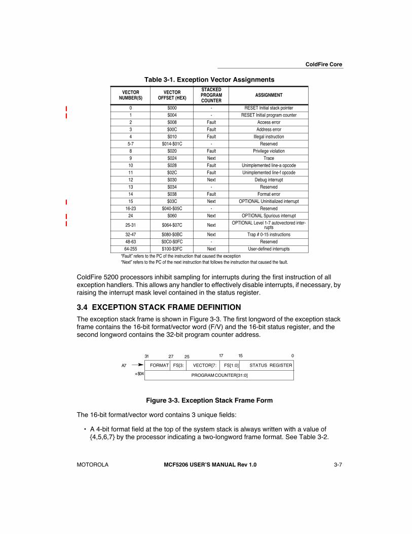
ColdFire Core
MOTOROLA
MCF5206 USERÕS MANUAL Rev 1.0
3-7
2
3
5
6
7
8
9
11
12
13
15
16
1
2
3
1
ColdFire 5200 processors inhibit sampling for interrupts during the first instruction of all exception handlers. This allows any handler to effectively disable interrupts, if necessary, by raising the interrupt mask level contained in the status register.
3.4 EXCEPTION STACK FRAME DEFINITION
The exception stack frame is shown in Figure 3-3. The first longword of the exception stack frame contains the 16-bit format/vector word (F/V) and the 16-bit status register, and the second longword contains the 32-bit program counter address.
The 16-bit format/vector word contains 3 unique fields:
¥ A 4-bit format field at the top of the system stack is always written with a value of {4,5,6,7} by the processor indicating a two-longword frame format. See Table 3-2.
Table 3-1. Exception Vector Assignments
VECTORNUMBER(S)
VECTOROFFSET (HEX)
STACKEDPROGRAMCOUNTER
ASSIGNMENT
0 $000 - RESET Initial stack pointer1 $004 - RESET Initial program counter2 $008 Fault Access error3 $00C Fault Address error4 $010 Fault Illegal instruction
5-7 $014-$01C - Reserved8 $020 Fault Privilege violation9 $024 Next Trace10 $028 Fault Unimplemented line-a opcode11 $02C Fault Unimplemented line-f opcode12 $030 Next Debug interrupt13 $034 - Reserved14 $038 Fault Format error15 $03C Next OPTIONAL Uninitialized interrupt
16-23 $040-$05C - Reserved24 $060 Next OPTIONAL Spurious interrupt
25-31 $064-$07C Next OPTIONAL Level 1-7 autovectored inter-rupts
32-47 $080-$0BC Next Trap # 0-15 instructions48-63 $0C0-$0FC - Reserved64-255 $100-$3FC Next User-defined interrupts
ÒFaultÓ refers to the PC of the instruction that caused the exceptionÒNextÓ refers to the PC of the next instruction that follows the instruction that caused the fault.
Figure 3-3. Exception Stack Frame Form
FORMAT FS[3: VECTOR[7: FS[1:0] STATUS REGISTER
PROGRAM COUNTER[31:0]
A7
+ $04
31 17 15 027 25

ColdFire Core
3-8
MCF5206 USERÕS MANUAL Rev 1.0
MOTOROLA
2
3
4
5
6
7
8
9
10
12
13
14
15
16
1
¥ A 4-bit fault status field, FS[3:0], at the top of the system stack. This field is defined for access and address errors only and written as zeros for all other types of exceptions. See Table 3-3.
¥ The 8-bit vector number, vector[7:0], defines the exception type and is calculated by the processor for all internal faults and represents the value supplied by the peripheral in the case of an interrupt. Refer to Table 3-1.
3.5 PROCESSOR EXCEPTIONS
3.5.1 Access Error Exception
An Access Error Exception vector number $2 occurs when a bus cycle terminates with an error condition. The exact processor response to an access error depends on the type of memory reference being performed.
For an instruction fetch, the processor postpones the error reporting until the faulted reference is needed by an instruction for execution. Therefore, faults that occur during instruction prefetches that are then followed by a change of instruction flow does not generate an exception. When the processor attempts to execute an instruction with a faulted opword and/or extension words, the access error is signaled and the instruction aborted. For this type of exception, the programming model has not been altered by the instruction generating the access error.
Table 3-2. Format Field Encodings
ORIGINAL A7 @ TIME OF EXCEPTION, BITS 1:0
A7 @ 1ST INSTRUCTION OF HANDLER
FORMAT FIELD
00 Original A7 - 8 401 Original A7 - 9 510 Original A7 - 10 611 Original A7 - 11 7
Table 3-3. Fault Status Encodings
FS[3:0] DEFINITION
00xx Reserved
0100 Error on instruction fetch
0101 Reserved
011x Reserved
1000 Error on operand write
1001 Attempted write to write-protected space
101x Reserved
1100 Error on operand read
1101 Reserved
111x Reserved
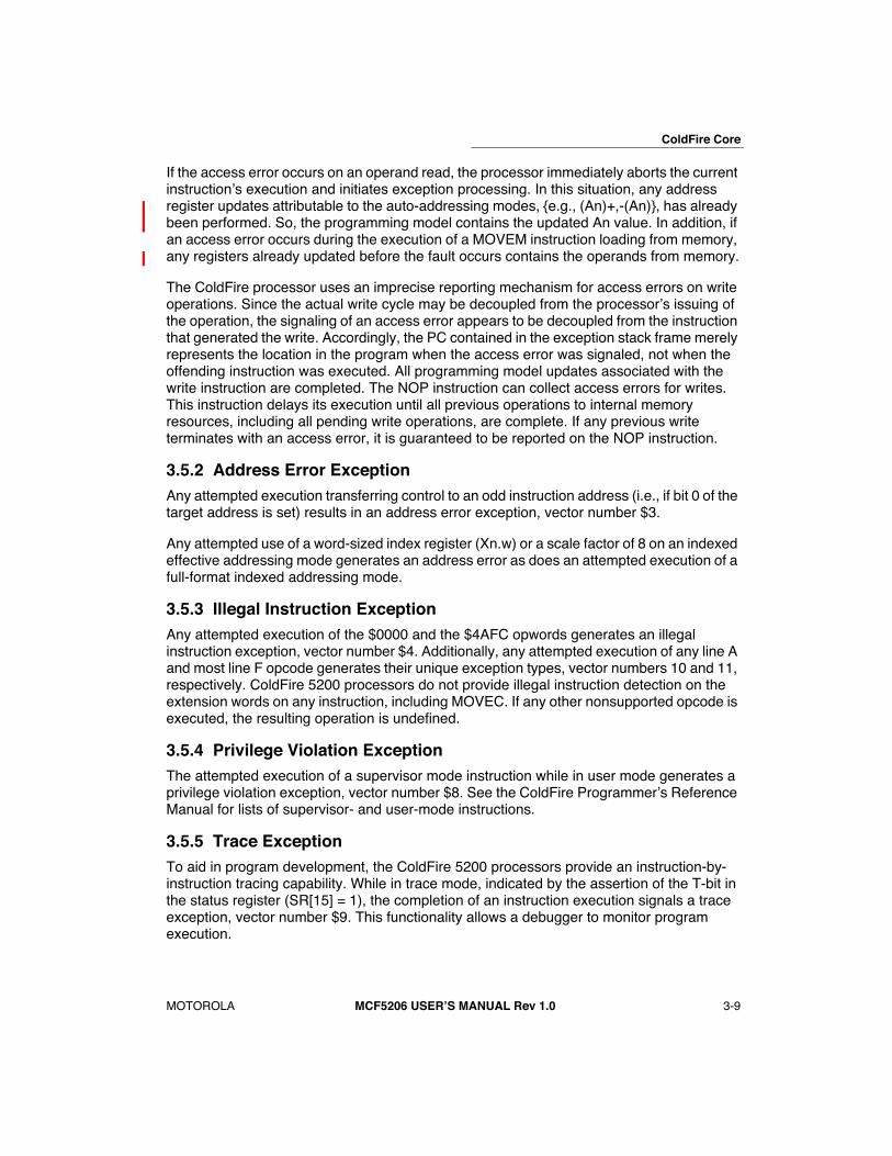
ColdFire Core
MOTOROLA
MCF5206 USERÕS MANUAL Rev 1.0
3-9
2
3
5
6
7
8
9
11
12
13
15
16
1
2
3
1
If the access error occurs on an operand read, the processor immediately aborts the current instructionÕs execution and initiates exception processing. In this situation, any address register updates attributable to the auto-addressing modes, {e.g., (An)+,-(An)}, has already been performed. So, the programming model contains the updated An value. In addition, if an access error occurs during the execution of a MOVEM instruction loading from memory, any registers already updated
before
the fault occurs contains the operands from memory.
The ColdFire processor uses an imprecise reporting mechanism for access errors on write operations. Since the actual write cycle may be decoupled from the processorÕs issuing of the operation, the signaling of an access error appears to be decoupled from the instruction that generated the write. Accordingly, the PC contained in the exception stack frame merely represents the location in the program when the access error was signaled, not when the offending instruction was executed. All programming model updates associated with the write instruction are completed. The NOP instruction can collect access errors for writes. This instruction delays its execution until all previous operations to internal memory resources, including all pending write operations, are complete. If any previous write terminates with an access error, it is guaranteed to be reported on the NOP instruction.
3.5.2 Address Error Exception
Any attempted execution transferring control to an odd instruction address (i.e., if bit 0 of the target address is set) results in an address error exception, vector number $3.
Any attempted use of a word-sized index register (Xn.w) or a scale factor of 8 on an indexed effective addressing mode generates an address error as does an attempted execution of a full-format indexed addressing mode.
3.5.3 Illegal Instruction Exception
Any attempted execution of the $0000 and the $4AFC opwords generates an illegal instruction exception, vector number $4. Additionally, any attempted execution of any line A and most line F opcode generates their unique exception types, vector numbers 10 and 11, respectively. ColdFire 5200 processors do not provide illegal instruction detection on the extension words on any instruction, including MOVEC. If any other nonsupported opcode is executed, the resulting operation is undefined.
3.5.4 Privilege Violation Exception
The attempted execution of a supervisor mode instruction while in user mode generates a privilege violation exception, vector number $8. See the
ColdFire ProgrammerÕs Reference Manual
for lists of supervisor- and user-mode instructions.
3.5.5 Trace Exception
To aid in program development, the ColdFire 5200 processors provide an instruction-by-instruction tracing capability. While in trace mode, indicated by the assertion of the T-bit in the status register (SR[15] = 1), the completion of an instruction execution signals a trace exception, vector number $9. This functionality allows a debugger to monitor program execution.
ColdFire Core
3-10
MCF5206 USERÕS MANUAL Rev 1.0
MOTOROLA
2
3
4
5
6
7
8
9
10
12
13
14
15
16
1
The single exception to this definition is the STOP instruction. When the STOP opcode is executed, the processor core waits until an unmasked interrupt request is asserted, then aborts the pipeline and initiates interrupt exception processing.
Because ColdFire processors do not support any hardware stacking of multiple exceptions, it is the responsibility of the operating system to check for trace mode after processing other exception types. As an example, consider the execution of a TRAP instruction while in trace mode. The processor initiates the TRAP exception and then pass control to the corresponding handler. If the system requires that a trace exception be processed, it is the responsibility of the TRAP exception handler to check for this condition (SR[15] in the exception stack frame asserted) and pass control to the trace handler before returning from the original exception.
3.5.6 Debug Interrupt
This exception is generated in response to a hardware breakpoint register trigger. The processor does not generate an IACK cycle but rather calculates the vector number internally (vector number 12).
3.5.7 RTE and Format Error Exceptions
When an RTE instruction is executed, the processor first examines the 4-bit format field in the exception stack frame on the stack to validate the frame type. For a ColdFire 5200 processor, any attempted execution of an RTE where the format is not equal to {4,5,6,7} generates a format error, vector number $E. The exception stack frame for the format error is created without disturbing the original RTE frame and the stacked PC pointing to the RTE instruction.
The selection of the format value provides some limited debug support for porting code from 68000 applications. On 680x0 family processors, the SR was located at the top of the stack. On those processors, bit[30] of the longword addressed by the system stack pointer is typically zero. Thus, if an RTE is attempted with a 680X0-type exception stack frame, the 5206 generates a format exception.
If the format field defines a valid type, the processor: (1) reloads the SR operand, (2) fetches the second longword operand, PC, (3) adjusts the stack pointer by adding the format value to the auto-incremented address after the fetch of the first longword, and then (4) transfers control to the instruction address defined by the PC (fetched in step2) second longword operand within the stack frame.
3.5.8 TRAP Instruction Exceptions
The TRAP #n
instruction always forces an exception as part of its execution and is useful for implementing system calls.
3.5.9 Interrupt Exception
The interrupt exception processing, with interrupt recognition and vector fetching, includes uninitialized and spurious interrupts as well as those where the requesting device supplies the 8-bit interrupt vector. Autovectoring may optionally be supported through the System
ColdFire Core
MOTOROLA
MCF5206 USERÕS MANUAL Rev 1.0
3-11
2
3
5
6
7
8
9
11
12
13
15
16
1
2
3
1
Integration module (SIM). Refer to the SIM section to see if this is supported on the MCF5206.
3.5.10 Fault-on-Fault Halt
If a ColdFire 5200 processor encounters any type of fault during the exception processing of another fault, the processor immediately halts execution with the catastrophic Òfault-on-faultÓ condition. A reset is required to force the processor to exit this halted state.
3.5.11 Reset Exception
Asserting the reset input signal to the processor causes a reset exception, vector number $0. The reset exception has the highest priority of any exception; it provides for system initialization and recovery from catastrophic failure. Reset also aborts any processing in progress when the reset input is recognized, and the aborted processing cannot be recovered.
The reset exception places the processor in the supervisor mode by setting the S-bit and disables tracing by clearing the T-bit in the SR. This exception also clears the M-bit and sets the processorÕs interrupt priority mask in the SR to the highest level (level 7). Next, the VBR is initialized to zero ($00000000). The control registers specifying the operation of any memories (e.g., cache and/or RAM modules) connected directly to the processor are disabled.
Note
Other implementation-specific supervisor registers are also affected. Refer to each of the modules in this userÕs manual fordetails on these registers.
Once the processor is granted the bus and it does not detect any other external masters taking the bus, the core then performs two longword read bus cycles. The first longword at address 0 is loaded into the stack pointer and the second longword at address 4 is loaded into the program counter. After the initial instruction is fetched from memory, program execution begins at the address in the PC. If an access error or address error occurs before the first instruction is executed, the processor enters the fault-on-fault halted state.
3.6 INSTRUCTION EXECUTION TIMING
This section presents ColdFire 5200 Family processor instruction execution times in terms of processor core clock cycles. The number of operand references for each instruction is enclosed in parentheses following the number of clock cycles. Each timing entry is presented as
C
(r/w) where:
¥
C
- number of processor clock cycles, including all applicable operand fetches and writes, and all internal core cycles required to complete the instruction execution.
¥ r/w - number of operand reads (r) and writes (w) required by the instruction. An operation performing a read-modify-write function is denoted as (1/1).
This section includes the assumptions concerning the timing values and the execution time details.

ColdFire Core
3-12
MCF5206 USERÕS MANUAL Rev 1.0
MOTOROLA
2
3
4
5
6
7
8
9
10
12
13
14
15
16
1
3.6.1 Timing Assumptions
For the timing data presented in this section, the following assumptions apply:
1. The operand execution pipeline (OEP) is loaded with the opword and all required ex-tension words at the beginning of each instruction execution. This implies that the OEP does not wait for the instruction fetch pipeline (IFP) to supply opwords and/or exten-sion words.
2. The OEP does not experience any sequence-related pipeline stalls. For ColdFire 5200 processors, the most common example of this type of stall involves consecutive store operations, excluding the MOVEM instruction. For all STORE operations (except MOVEM), certain hardware resources within the processor are marked as ÒbusyÓ for two clock cycles after the final DSOC cycle of the store instruction. If a subsequent STORE instruction is encountered within this 2-cycle window, it is stalled until the re-source again becomes available. Thus, the maximum pipeline stall involving consec-utive STORE operations is 2 cycles. The MOVEM instruction uses a different set of resources and this stall does not apply.
3. The OEP completes all memory accesses without any stall conditions caused by the memory itself. Thus, the timing details provided in this section assume that an infinite zero-wait state memory is attached to the processor core.
4. All operand data accesses are aligned on the same byte boundary as the operand size, i.e., 16-bit operands aligned on 0-modulo-2 addresses, 32-bit operands aligned on 0-modulo-4 addresses.
If the operand alignment fails these guidelines, it is misaligned. The processor core decomposes the misaligned operand reference into a series of aligned accesses as shown in Table 3-4.
3.6.2 MOVE Instruction Execution Times
The execution times for the MOVE.{B,W} instructions are shown in Table 3-5, while Table 3-6 provides the timing for MOVE.L.
For all
tables in this section, the execution time of any instruction using the PC-relative effective addressing modes is the same for the comparable An-relative mode.
The nomenclature Òxxx.wlÓ refers to both forms of absolute addressing, xxx.w and xxx.l.
Table 3-4. Misaligned Operand References
ADDRESS[1:0] SIZEKBUS
OPERATIONSADDITIONAL
C(R/W)
X1 Word Byte, Byte 2(1/0) if read1(0/1) if write
X1 Long Byte, Word, Byte 3(2/0) if read2(0/2) if write
10 Long Word, Word 2(1/0) if read1(0/1) if write

ColdFire Core
MOTOROLA
MCF5206 USERÕS MANUAL Rev 1.0
3-13
2
3
5
6
7
8
9
11
12
13
15
16
1
2
3
1
Table 3-5. Move Byte and Word Execution Times
SOURCEDESTINATION
RX (AX) (AX)+ -(AX) (D16,AX) (D8,AX,XN*SF) XXX.WL
Dy 1(0/0) 1(0/1) 1(0/1) 1(0/1) 1(0/1) 2(0/1) 1(0/1)Ay 1(0/0) 1(0/1) 1(0/1) 1(0/1) 1(0/1) 2(0/1) 1(0/1)
(Ay) 3(1/0) 3(1/1) 3(1/1) 3(1/1) 3(1/1) 4(1/1) 3(1/1)(Ay)+ 3(1/0) 3(1/1) 3(1/1) 3(1/1) 3(1/1) 4(1/1) 3(1/1)-(Ay) 3(1/0) 3(1/1) 3(1/1) 3(1/1) 3(1/1) 4(1/1) 3(1/1)
(d16,Ay) 3(1/0) 3(1/1) 3(1/1) 3(1/1) 3(1/1) Ñ Ñ(d8,Ay,Xn*SF) 4(1/0) 4(1/1) 4(1/1) 4(1/1) Ñ Ñ Ñ
xxx.w 3(1/0) 3(1/1) 3(1/1) 3(1/1) Ñ Ñ Ñxxx.l 3(1/0) 3(1/1) 3(1/1) 3(1/1) Ñ Ñ Ñ
(d16,PC) 3(1/0) 3(1/1) 3(1/1) 3(1/1) 3(1/1) Ñ Ñ(d8,PC,Xn*SF) 4(1/0) 4(1/1) 4(1/1) 4(1/1) Ñ Ñ Ñ
#xxx 1(0/0) 3(0/1) 3(0/1) 3(0/1) Ñ Ñ Ñ
Table 3-6. Move Long Execution Times
SOURCEDESTINATION
RX (AX) (AX)+ -(AX) (D16,AX) (D8,AX,XN*SF) XXX.WL
Dy 1(0/0) 1(0/1) 1(0/1) 1(0/1) 1(0/1) 2(0/1) 1(0/1)Ay 1(0/0) 1(0/1) 1(0/1) 1(0/1) 1(0/1) 2(0/1) 1(0/1)
(Ay) 2(1/0) 2(1/1) 2(1/1) 2(1/1) 2(1/1) 3(1/1) 2(1/1)(Ay)+ 2(1/0) 2(1/1) 2(1/1) 2(1/1) 2(1/1) 3(1/1) 2(1/1)-(Ay) 2(1/0) 2(1/1) 2(1/1) 2(1/1) 2(1/1) 3(1/1) 2(1/1)
(d16,Ay) 2(1/0) 2(1/1) 2(1/1) 2(1/1) 2(1/1) Ñ Ñ(d8,Ay,Xn*SF) 3(1/0) 3(1/1) 3(1/1) 3(1/1) Ñ Ñ Ñ
xxx.w 2(1/0) 2(1/1) 2(1/1) 2(1/1) Ñ Ñ Ñxxx.l 2(1/0) 2(1/1) 2(1/1) 2(1/1) Ñ Ñ Ñ
(d16,PC) 2(1/0) 2(1/1) 2(1/1) 2(1/1) 2(1/1) Ñ Ñ(d8,PC,Xn*SF) 3(1/0) 3(1/1) 3(1/1) 3(1/1) Ñ Ñ Ñ
#xxx 1(0/0) 2(0/1) 2(0/1) 2(0/1) Ñ Ñ Ñ

ColdFire Core
3-14
MCF5206 USERÕS MANUAL Rev 1.0
MOTOROLA
2
3
4
5
6
7
8
9
10
12
13
14
15
16
1
3.7 STANDARD ONE OPERAND INSTRUCTION EXECUTION TIMES
Table 3-7. One Operand Instruction Execution Times
OPCODE <EA>EFFECTIVE ADDRESS
RN (AN) (AN)+ -(AN) (D16,AN) (D8,AN,XN*SF) XXX.WL #XXX
CLR.B <ea> 1(0/0) 1(0/1) 1(0/1) 1(0/1) 1(0/1) 2(0/1) 1(0/1) ÑCLR.W <ea> 1(0/0) 1(0/1) 1(0/1) 1(0/1) 1(0/1) 2(0/1) 1(0/1) ÑCLR.L <ea> 1(0/0) 1(0/1) 1(0/1) 1(0/1) 1(0/1) 2(0/1) 1(0/1) ÑEXT.W Dx 1(0/0) Ñ Ñ Ñ Ñ Ñ Ñ ÑEXT.L Dx 1(0/0) Ñ Ñ Ñ Ñ Ñ Ñ Ñ
EXTB.L Dx 1(0/0) Ñ Ñ Ñ Ñ Ñ Ñ ÑNEG.L Dx 1(0/0) Ñ Ñ Ñ Ñ Ñ Ñ Ñ
NEGX.L Dx 1(0/0) Ñ Ñ Ñ Ñ Ñ Ñ ÑNOT.L Dx 1(0/0) Ñ Ñ Ñ Ñ Ñ Ñ Ñ
Scc Dx 1(0/0) Ñ Ñ Ñ Ñ Ñ Ñ ÑSWAP Dx 1(0/0) Ñ Ñ Ñ Ñ Ñ Ñ ÑTST.B <ea> 1(0/0) 3(1/0) 3(1/0) 3(1/0) 3(1/0) 4(1/0) 3(1/0) 1(0/0)TST.W <ea> 1(0/0) 3(1/0) 3(1/0) 3(1/0) 3(1/0) 4(1/0) 3(1/0) 1(0/0)TST.L <ea> 1(0/0) 2(1/0) 2(1/0) 2(1/0) 2(1/0) 3(1/0) 2(1/0) 1(0/0)
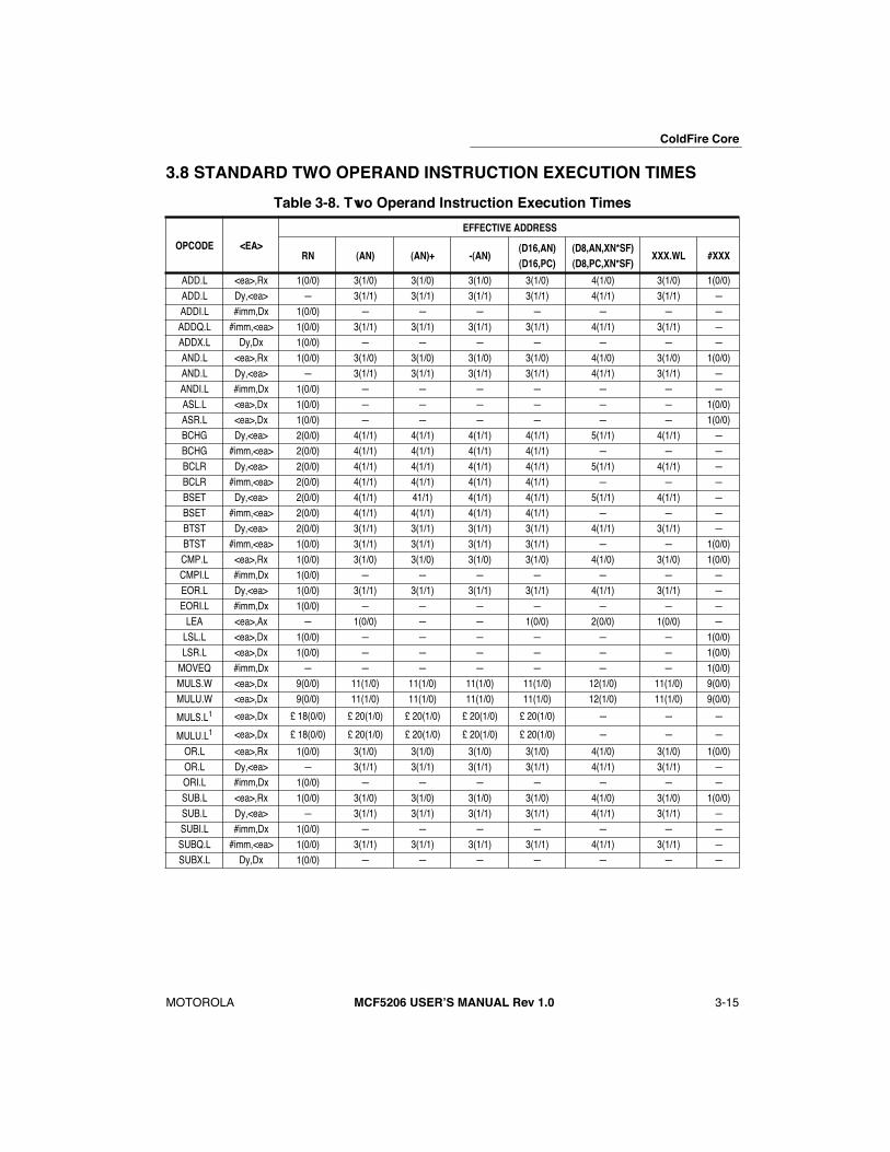
ColdFire Core
MOTOROLA
MCF5206 USERÕS MANUAL Rev 1.0
3-15
2
3
5
6
7
8
9
11
12
13
15
16
1
2
3
1
3.8 STANDARD TWO OPERAND INSTRUCTION EXECUTION TIMES
Table 3-8. Two Operand Instruction Execution Times
OPCODE <EA>
EFFECTIVE ADDRESS
RN (AN) (AN)+ -(AN)(D16,AN)(D16,PC)
(D8,AN,XN*SF) (D8,PC,XN*SF)
XXX.WL #XXX
ADD.L <ea>,Rx 1(0/0) 3(1/0) 3(1/0) 3(1/0) 3(1/0) 4(1/0) 3(1/0) 1(0/0)ADD.L Dy,<ea> Ñ 3(1/1) 3(1/1) 3(1/1) 3(1/1) 4(1/1) 3(1/1) ÑADDI.L #imm,Dx 1(0/0) Ñ Ñ Ñ Ñ Ñ Ñ ÑADDQ.L #imm,<ea> 1(0/0) 3(1/1) 3(1/1) 3(1/1) 3(1/1) 4(1/1) 3(1/1) ÑADDX.L Dy,Dx 1(0/0) Ñ Ñ Ñ Ñ Ñ Ñ ÑAND.L <ea>,Rx 1(0/0) 3(1/0) 3(1/0) 3(1/0) 3(1/0) 4(1/0) 3(1/0) 1(0/0)AND.L Dy,<ea> Ñ 3(1/1) 3(1/1) 3(1/1) 3(1/1) 4(1/1) 3(1/1) ÑANDI.L #imm,Dx 1(0/0) Ñ Ñ Ñ Ñ Ñ Ñ ÑASL.L <ea>,Dx 1(0/0) Ñ Ñ Ñ Ñ Ñ Ñ 1(0/0)ASR.L <ea>,Dx 1(0/0) Ñ Ñ Ñ Ñ Ñ Ñ 1(0/0)BCHG Dy,<ea> 2(0/0) 4(1/1) 4(1/1) 4(1/1) 4(1/1) 5(1/1) 4(1/1) ÑBCHG #imm,<ea> 2(0/0) 4(1/1) 4(1/1) 4(1/1) 4(1/1) Ñ Ñ ÑBCLR Dy,<ea> 2(0/0) 4(1/1) 4(1/1) 4(1/1) 4(1/1) 5(1/1) 4(1/1) ÑBCLR #imm,<ea> 2(0/0) 4(1/1) 4(1/1) 4(1/1) 4(1/1) Ñ Ñ ÑBSET Dy,<ea> 2(0/0) 4(1/1) 41/1) 4(1/1) 4(1/1) 5(1/1) 4(1/1) ÑBSET #imm,<ea> 2(0/0) 4(1/1) 4(1/1) 4(1/1) 4(1/1) Ñ Ñ ÑBTST Dy,<ea> 2(0/0) 3(1/1) 3(1/1) 3(1/1) 3(1/1) 4(1/1) 3(1/1) ÑBTST #imm,<ea> 1(0/0) 3(1/1) 3(1/1) 3(1/1) 3(1/1) Ñ Ñ 1(0/0)CMP.L <ea>,Rx 1(0/0) 3(1/0) 3(1/0) 3(1/0) 3(1/0) 4(1/0) 3(1/0) 1(0/0)CMPI.L #imm,Dx 1(0/0) Ñ Ñ Ñ Ñ Ñ Ñ ÑEOR.L Dy,<ea> 1(0/0) 3(1/1) 3(1/1) 3(1/1) 3(1/1) 4(1/1) 3(1/1) ÑEORI.L #imm,Dx 1(0/0) Ñ Ñ Ñ Ñ Ñ Ñ Ñ
LEA <ea>,Ax Ñ 1(0/0) Ñ Ñ 1(0/0) 2(0/0) 1(0/0) ÑLSL.L <ea>,Dx 1(0/0) Ñ Ñ Ñ Ñ Ñ Ñ 1(0/0)LSR.L <ea>,Dx 1(0/0) Ñ Ñ Ñ Ñ Ñ Ñ 1(0/0)
MOVEQ #imm,Dx Ñ Ñ Ñ Ñ Ñ Ñ Ñ 1(0/0)MULS.W <ea>,Dx 9(0/0) 11(1/0) 11(1/0) 11(1/0) 11(1/0) 12(1/0) 11(1/0) 9(0/0)MULU.W <ea>,Dx 9(0/0) 11(1/0) 11(1/0) 11(1/0) 11(1/0) 12(1/0) 11(1/0) 9(0/0)
MULS.L
1
<ea>,Dx £ 18(0/0) £ 20(1/0) £ 20(1/0) £ 20(1/0) £ 20(1/0) Ñ Ñ Ñ
MULU.L
1
<ea>,Dx £ 18(0/0) £ 20(1/0) £ 20(1/0) £ 20(1/0) £ 20(1/0) Ñ Ñ Ñ
OR.L <ea>,Rx 1(0/0) 3(1/0) 3(1/0) 3(1/0) 3(1/0) 4(1/0) 3(1/0) 1(0/0)OR.L Dy,<ea> Ñ 3(1/1) 3(1/1) 3(1/1) 3(1/1) 4(1/1) 3(1/1) ÑORI.L #imm,Dx 1(0/0) Ñ Ñ Ñ Ñ Ñ Ñ ÑSUB.L <ea>,Rx 1(0/0) 3(1/0) 3(1/0) 3(1/0) 3(1/0) 4(1/0) 3(1/0) 1(0/0)SUB.L Dy,<ea> Ñ 3(1/1) 3(1/1) 3(1/1) 3(1/1) 4(1/1) 3(1/1) ÑSUBI.L #imm,Dx 1(0/0) Ñ Ñ Ñ Ñ Ñ Ñ ÑSUBQ.L #imm,<ea> 1(0/0) 3(1/1) 3(1/1) 3(1/1) 3(1/1) 4(1/1) 3(1/1) ÑSUBX.L Dy,Dx 1(0/0) Ñ Ñ Ñ Ñ Ñ Ñ Ñ

ColdFire Core
3-16
MCF5206 USERÕS MANUAL Rev 1.0
MOTOROLA
2
3
4
5
6
7
8
9
10
12
13
14
15
16
1
3.9 MISCELLANEOUS INSTRUCTION EXECUTION TIMES
Table 3-9. Miscellaneous Instruction Execution Times
OPCODE <EA>EFFECTIVE ADDRESS
RN (AN) (AN)+ -(AN) (D16,AN) (D8,AN,XN*SF) XXX.WL #XXX
LINK.W Ay,#imm 2(0/1) Ñ Ñ Ñ Ñ Ñ Ñ ÑMOVE.W CCR,Dx 1(0/0) Ñ Ñ Ñ Ñ Ñ Ñ ÑMOVE.W <ea>,CCR 1(0/0) Ñ Ñ Ñ Ñ Ñ Ñ 1(0/0)MOVE.W SR,Dx 1(0/0) Ñ Ñ Ñ Ñ Ñ Ñ Ñ
MOVE.W <ea>,SR 7(0/0) Ñ Ñ Ñ Ñ Ñ Ñ 7(0/0)
2
MOVEC Ry,Rc 9(0/1) Ñ Ñ Ñ Ñ Ñ Ñ ÑMOVEM.L <ea>,&list Ñ 1+n(n/0) Ñ Ñ 1+n(n/0) Ñ Ñ ÑMOVEM.L &list,<ea> Ñ 1+n(0/n) Ñ Ñ 1+n(0/n) Ñ Ñ Ñ
NOP 3(0/0) Ñ Ñ Ñ Ñ Ñ Ñ Ñ
PEA <ea> Ñ 2(0/1) Ñ Ñ 2(0/1)
4
3(0/1)
5
2(0/1) Ñ
PULSE 1(0/0) Ñ Ñ Ñ Ñ Ñ Ñ Ñ
STOP #imm Ñ Ñ Ñ Ñ Ñ Ñ Ñ 3(0/0)
3
TRAP #imm Ñ Ñ Ñ Ñ Ñ Ñ Ñ 15(1/2)TRAPF 1(0/0) Ñ Ñ Ñ Ñ Ñ Ñ Ñ
TRAPF.W 1(0/0) Ñ Ñ Ñ Ñ Ñ Ñ ÑTRAPF.L 1(0/0) Ñ Ñ Ñ Ñ Ñ Ñ Ñ
UNLK Ax 2(1/0) Ñ Ñ Ñ Ñ Ñ Ñ ÑWDDATA <ea> Ñ 3(1/0) 3(1/0) 3(1/0) 3(1/0) 4(1/0) 3(1/0) 3(1/0)WDEBUG <ea> Ñ 5(2/0) Ñ Ñ 5(2/0) Ñ Ñ Ñ
n is the number of registers moved by the MOVEM opcode.
1
£ indicates that long multiplies have early termination after 9 cycles; thus, actual cycle count is operand independent
2
If a MOVE.W #imm,SR instruction is executed and imm[13] = 1, the execution time is 1(0/0).
3
The execution time for STOP is the time required until the processor begins sampling continuously for interrupts.
4
PEA execution times are the same for (d16,PC)
5
PEA execution times are the same for (d8,PC,Xn*SF)

ColdFire Core
MOTOROLA MCF5206 USERÕS MANUAL Rev 1.0 3-17
2
3
5
6
7
8
9
11
12
13
15
16
1
2
3
13.10 BRANCH INSTRUCTION EXECUTION TIMES
Table 3-10. General Branch Instruction Execution Times
OPCODE <EA>
EFFECTIVE ADDRESS
RN (AN) (AN)+ -(AN)(D16,AN)(D16,PC)
(D8,AN,XI*SF) (D8,PC,XI*SF)
XXX.WL #XXX
BSR Ñ Ñ Ñ Ñ 3(0/1) Ñ Ñ ÑJMP <ea> Ñ 3(0/0) Ñ Ñ 3(0/0) 4(0/0) 3(0/0) ÑJSR <ea> Ñ 3(0/1) Ñ Ñ 3(0/1) 4(0/1) 3(0/1) ÑRTE Ñ Ñ 10(2/0) Ñ Ñ Ñ Ñ ÑRTS Ñ Ñ 5(1/0) Ñ Ñ Ñ Ñ Ñ
Table 3-11. BRA, Bcc Instruction Execution Times
OPCODEFORWARD
TAKENFORWARD
NOT TAKENBACKWARD
TAKENBACKWARDNOT TAKEN
BRA 2(0/0) Ñ 2(0/0) ÑBcc 3(0/0) 1(0/0) 2(0/0) 3(0/0)

ColdFire Core
3-18 MCF5206 USERÕS MANUAL Rev 1.0 MOTOROLA
2
3
4
5
6
7
8
9
10
12
13
14
15
16
1

MOTOROLA
MCF5206 USERÕS MANUAL Rev 1.0
4-1
SECTION 4INSTRUCTION CACHE
4.1 FEATURES OF INSTRUCTION CACHE
¥ 512-Byte Direct-Mapped Cache
¥ Single-Cycle Access on Cache Hits
¥ Physically Located on ColdFire core's High-Speed Local Bus
¥ Nonblocking Design to Maximize Performance
¥ 16-Byte Line-Fill Buffer
¥ Configurable Cache-Miss Fetch Algorithm
4.2 INSTRUCTION CACHE PHYSICAL ORGANIZATION
The instruction cache is a direct-mapped single-cycle memory, organized as 32 lines, each containing 16 bytes. The memory storage consists of a 32-entry tag array (containing addresses and a valid bit), and the data array containing 512 bytes of instruction data, organized as 128 x 32 bits.
The two memory arrays are accessed in parallel: bits [8:4] of the instruction fetch address provide the index into the tag array, and bits [8:2] addressing the data array. The tag array outputs the address mapped to the given cache location along with the valid bit for the line. This address field is compared to bits [31:9] of the instruction fetch address from the local bus to determine if a cache hit in the memory array has occurred. If the desired address is mapped into the cache memory, the output of the data array is driven onto the ColdFire core's local data bus completing the access in a single cycle.
The tag array maintains a single valid bit per line entry. Accordingly, only entire 16-byte lines are loaded into the instruction cache.
The instruction cache also contains a 16-byte fill buffer that provides temporary storage for the last line fetched in response to a cache miss. With each instruction fetch, the contents of the line fill buffer are examined. Thus, each instruction fetch address examines both the tag memory array and the line fill buffer to see if the desired address is mapped into either hardware resource, with the linefill buffer having priority over the instruction cache. A cache hit in either the memory array or the line-fill buffer is serviced in a single cycle. Because the line fill buffer maintains valid bits on a longword basis, hits in the buffer can be serviced immediately without waiting for the entire line to be fetched.
DATE: 8-28-98REVISION NO.: 1.1PAGES AFFECTED: SEE CHANGE BARS

Instruction Cache
4-2
MCF5206 USERÕS MANUAL Rev 1.0
MOTOROLA
If the referenced address is not contained in the memory array or the line-fill buffer, the instruction cache initiates the required external fetch operation. In most situations, this is a 16-byte line-sized burst reference.
The hardware implementation is a nonblocking design, meaning the ColdFire core's local bus is released after the initial access of a miss. Thus, the cache or the SRAM module can service subsequent requests while the remainder of the line is being fetched and loaded into the fill buffer.
Figure 4-1. Instruction Cache Block Diagram
4.3 INSTRUCTION CACHE OPERATION
The instruction cache is physically connected to the ColdFire core's local bus, allowing it to service all instruction fetches from the ColdFire core and certain memory fetches initiated by the debug module. Typically, the Debug module's memory references appear as supervisor data accesses, but the unit can be programmed to generate user-mode accesses and/or instruction fetches. The instruction cache processes any instruction fetch access in the normal manner.
31 9 8 4 3 012 31 4
=
=
31 9 31 0
Ô12731
00
LOCAL ADDRESS BUS
LINE BUFFERADDRESS
EXTERNAL DATA[31:0]
LINE BUFFER DATA STORAGE
MUX
DATA
MUX
FILL HIT
TAG
VALI
D
LOCAL DATA BUSTAG HIT

Instruction Cache
MOTOROLA
MCF5206 USERÕS MANUAL Rev 1.0
4-3
4.3.1 Interaction With Other Modules
Since the instruction cache and high-speed SRAM module are connected to the ColdFire core's local data bus, certain user-defined configurations can result in simultaneous instruction fetch processing.
If the referenced address is mapped into the SRAM module, that module will service the request in a single cycle. In this case, data accessed from the instruction cache is simply discarded, and no external memory references are generated. If the address is not mapped into the SRAM space, the instruction cache handles the request in the normal fashion.
4.3.2 Memory Reference Attributes
For every memory reference the ColdFire core or the Debug module generates, a set of Òeffective attributesÓ is determined based on the address and the Access Control Registers (ACR0, ACR1). This set of attributes includes the cacheable/noncacheable definition, the precise/imprecise handling of operand write, and the write-protect capability.
In particular, each address is compared to the values programmed in the Access Control Registers (ACR). If the address matches one of the ACR values, the access attributes from that ACR are applied to the reference. If the address does not match either ACR, then the default value defined in the Cache Control Register (CACR) is used. The specific algorithm is as follows:
if (address = ACR0_address including mask) Effective Attributes = ACR0 attributes else if (address = ACR1_address including mask) Effective Attributes = ACR1 attributes else Effective Attributes = CACR default attributes
4.3.3 Cache Coherency and Invalidation
The instruction cache does not monitor ColdFire core data references for accesses to cached instructions, therefore software must maintain cache coherency by invalidating the appropriate cache entries after modifying code segments.
The cache invalidation can be performed in two ways. The assertion of bit 24 in the CACR, via a CPU space write, forces the entire instruction cache to be marked as invalid. The invalidation operation requires 32 cycles because the cache sequences through the entire tag array, clearing a single location each cycle. Any subsequent instruction fetch accesses are postponed until the invalidation sequence is complete.
The privileged CPUSHL instruction can invalidate a single cache line. When this instruction is executed, the cache entry defined by bits[8:4] of the source address register is invalidated, provided bit 28 of the CACR is cleared.
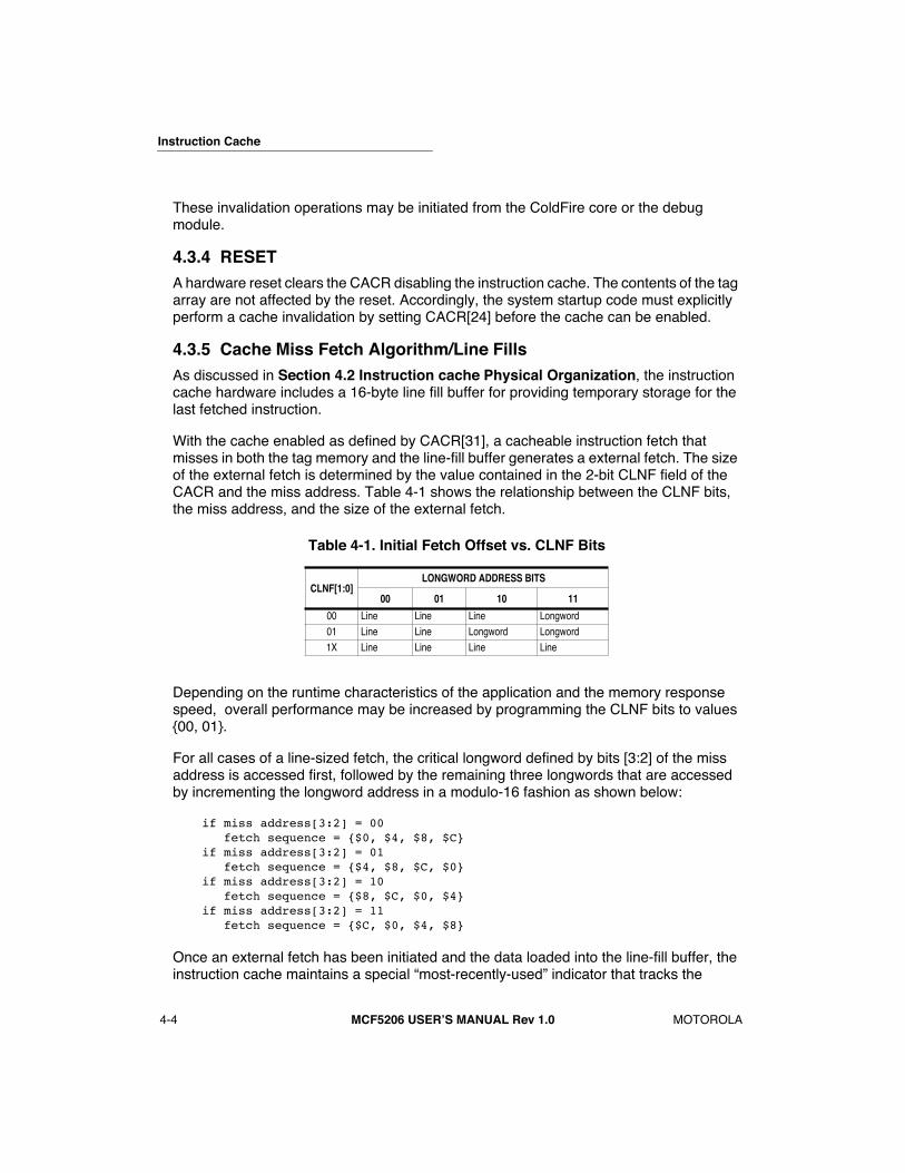
Instruction Cache
4-4
MCF5206 USERÕS MANUAL Rev 1.0
MOTOROLA
These invalidation operations may be initiated from the ColdFire core or the debug module.
4.3.4 RESET
A hardware reset clears the CACR disabling the instruction cache. The contents of the tag array are not affected by the reset. Accordingly, the system startup code must explicitly perform a cache invalidation by setting CACR[24] before the cache can be enabled.
4.3.5 Cache Miss Fetch Algorithm/Line Fills
As discussed in
Section 4.2 Instruction cache Physical Organization
, the instruction cache hardware includes a 16-byte line fill buffer for providing temporary storage for the last fetched instruction.
With the cache enabled as defined by CACR[31], a cacheable instruction fetch that misses in both the tag memory and the line-fill buffer generates a external fetch. The size of the external fetch is determined by the value contained in the 2-bit CLNF field of the CACR and the miss address. Table 4-1 shows the relationship between the CLNF bits, the miss address, and the size of the external fetch.
Depending on the runtime characteristics of the application and the memory response speed, overall performance may be increased by programming the CLNF bits to values {00, 01}.
For all cases of a line-sized fetch, the critical longword defined by bits [3:2] of the miss address is accessed first, followed by the remaining three longwords that are accessed by incrementing the longword address in a modulo-16 fashion as shown below:
if miss address[3:2] = 00 fetch sequence = {$0, $4, $8, $C} if miss address[3:2] = 01 fetch sequence = {$4, $8, $C, $0} if miss address[3:2] = 10 fetch sequence = {$8, $C, $0, $4} if miss address[3:2] = 11 fetch sequence = {$C, $0, $4, $8}
Once an external fetch has been initiated and the data loaded into the line-fill buffer, the instruction cache maintains a special Òmost-recently-usedÓ indicator that tracks the
Table 4-1. Initial Fetch Offset vs. CLNF Bits
CLNF[1:0]LONGWORD ADDRESS BITS
00 01 10 11
00 Line Line Line Longword01 Line Line Longword Longword1X Line Line Line Line
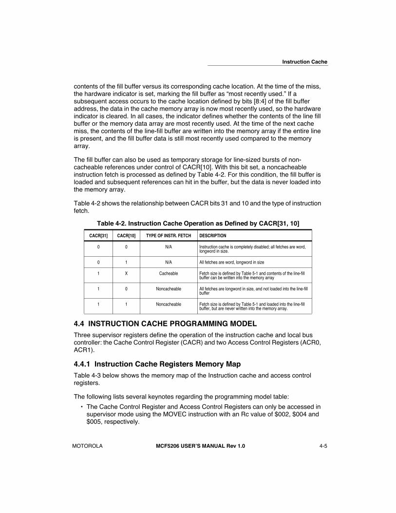
Instruction Cache
MOTOROLA
MCF5206 USERÕS MANUAL Rev 1.0
4-5
contents of the fill buffer versus its corresponding cache location. At the time of the miss, the hardware indicator is set, marking the fill buffer as Òmost recently used.Ó If a subsequent access occurs to the cache location defined by bits [8:4] of the fill buffer address, the data in the cache memory array is now most recently used, so the hardware indicator is cleared. In all cases, the indicator defines whether the contents of the line fill buffer or the memory data array are most recently used. At the time of the next cache miss, the contents of the line-fill buffer are written into the memory array if the entire line is present, and the fill buffer data is still most recently used compared to the memory array.
The fill buffer can also be used as temporary storage for line-sized bursts of non-cacheable references under control of CACR[10]. With this bit set, a noncacheable instruction fetch is processed as defined by Table 4-2. For this condition, the fill buffer is loaded and subsequent references can hit in the buffer, but the data is never loaded into the memory array.
Table 4-2 shows the relationship between CACR bits 31 and 10 and the type of instruction fetch.
4.4 INSTRUCTION CACHE PROGRAMMING MODEL
Three supervisor registers define the operation of the instruction cache and local bus controller: the Cache Control Register (CACR) and two Access Control Registers (ACR0, ACR1).
4.4.1 Instruction Cache Registers Memory Map
Table 4-3 below shows the memory map of the Instruction cache and access control registers.
The following lists several keynotes regarding the programming model table:
¥ The Cache Control Register and Access Control Registers can only be accessed in supervisor mode using the MOVEC instruction with an Rc value of $002, $004 and $005, respectively.
Table 4-2. Instruction Cache Operation as Defined by CACR[31, 10]
CACR[31] CACR[10] TYPE OF INSTR. FETCH DESCRIPTION
0 0 N/A Instruction cache is completely disabled; all fetches are word, longword in size.
0 1 N/A All fetches are word, longword in size
1 X Cacheable Fetch size is defined by Table 5-1 and contents of the line-fill buffer can be written into the memory array
1 0 Noncacheable All fetches are longword in size, and not loaded into the line-fill buffer
1 1 Noncacheable Fetch size is defined by Table 5-1 and loaded into the line-fill buffer, but are never written into the memory array.
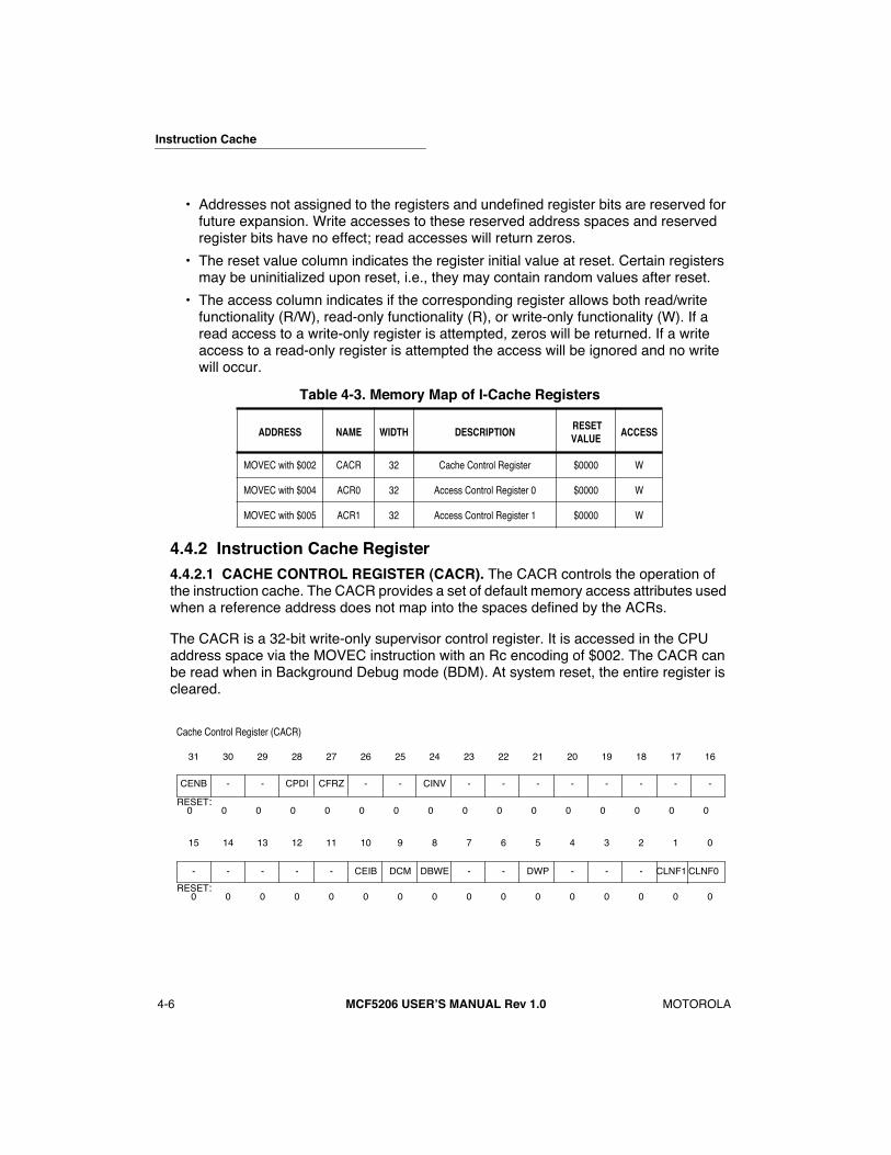
Instruction Cache
4-6
MCF5206 USERÕS MANUAL Rev 1.0
MOTOROLA
¥ Addresses not assigned to the registers and undefined register bits are reserved for future expansion. Write accesses to these reserved address spaces and reserved register bits have no effect; read accesses will return zeros.
¥ The reset value column indicates the register initial value at reset. Certain registers may be uninitialized upon reset, i.e., they may contain random values after reset.
¥ The access column indicates if the corresponding register allows both read/write functionality (R/W), read-only functionality (R), or write-only functionality (W). If a read access to a write-only register is attempted, zeros will be returned. If a write access to a read-only register is attempted the access will be ignored and no write will occur.
4.4.2 Instruction Cache Register
4.4.2.1 CACHE CONTROL REGISTER (CACR).
The CACR controls the operation of the instruction cache. The CACR provides a set of default memory access attributes used when a reference address does not map into the spaces defined by the ACRs.
The CACR is a 32-bit write-only supervisor control register. It is accessed in the CPU address space via the MOVEC instruction with an Rc encoding of $002. The CACR can be read when in Background Debug mode (BDM). At system reset, the entire register is cleared.
Table 4-3. Memory Map of I-Cache Registers
ADDRESS NAME WIDTH DESCRIPTION RESET VALUE
ACCESS
MOVEC with $002 CACR 32 Cache Control Register $0000 W
MOVEC with $004 ACR0 32 Access Control Register 0 $0000 W
MOVEC with $005 ACR1 32 Access Control Register 1 $0000 W
CENB - - CPDI CFRZ - - CINV - - - - - - - -
31 30 29 28 27 26 25 24 23 22 21 20 19 18 17 16
RESET:
- - - - - CEIB DCM DBWE - - DWP - - - CLNF1 CLNF0
15 14 13 12 11 10 9 8 7 6 5 4 3 2 1 0
0 0 0 0 0 0 0 0 0 0 0 0 0 0 0 0RESET:
0 0 0 0 0 0 0 0 0 0 0 0 0 0 0 0
Cache Control Register (CACR)

Instruction Cache
MOTOROLA
MCF5206 USERÕS MANUAL Rev 1.0
4-7
CENB - Cache Enable: CACR[31]When the cache is disabled, all instruction fetches generate word or longword-sized fetch. Generally, longword references are used for sequential fetches. If the processor branches to an odd word address, a word-sized fetch is generated. The memory array of the instruction cache is enabled only if CENB is asserted.
0 = Cache disabled1 = Cache enabled
CPDI - Disable CPUSHL Invalidation: CACR[28]When the privileged CPUSHL instruction is executed, the cache entry defined by bits [8:4] of the address is invalidated if CPDI = 0. If CPDI = 1, no operation is performed.
0 = Enable invalidation1 = Disable invalidation
CFRZ - Cache Freeze: CACR[27]This field allows the user to freeze the contents of the cache. When CFRZ is asserted, line fetches can be initiated and loaded into the line-fill buffer, but a valid cache entry is never overwritten. If a given cache location is invalid, the contents of the line-fill buffer can be written into the memory array while CFRZ is asserted.
0 = Normal Operation1 = Freeze valid cache lines
CINV - Cache Invalidate: CACR[24]Setting this bit forces the cache to invalid each tag array entry. The invalidation process requires 32 machine cycles, with a single cache entry cleared per machine cycle. The state of this bit is always read as a zero. After a hardware reset, the cache must be invalidated before it is enabled.
0 = No operation1 = Invalidate all cache locations
CIEB - Cache Enable Noncacheable Instruction Bursting: CACR[10]Setting this bit enables the line-fill buffer to be loaded with burst transfers under control of CLINF[1:0] for non-cacheable accesses. Noncacheable accesses are never written into the memory array.
0 = Disable burst fetches on noncacheable accesses1 = Enable burst fetches on noncacheable accesses
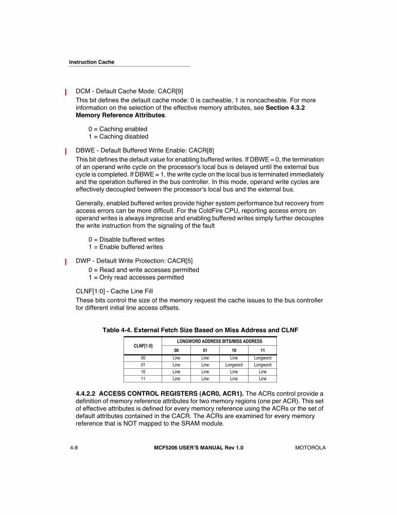
Instruction Cache
4-8
MCF5206 USERÕS MANUAL Rev 1.0
MOTOROLA
DCM - Default Cache Mode: CACR[9]This bit defines the default cache mode: 0 is cacheable, 1 is noncacheable. For more information on the selection of the effective memory attributes, see
Section 4.3.2 Memory Reference Attributes
.
0 = Caching enabled1 = Caching disabled
DBWE - Default Buffered Write Enable: CACR[8]This bit defines the default value for enabling buffered writes. If DBWE = 0, the termination of an operand write cycle on the processor's local bus is delayed until the external bus cycle is completed. If DBWE = 1, the write cycle on the local bus is terminated immediately and the operation buffered in the bus controller. In this mode, operand write cycles are effectively decoupled between the processor's local bus and the external bus.
Generally, enabled buffered writes provide higher system performance but recovery from access errors can be more difficult. For the ColdFire CPU, reporting access errors on operand writes is always imprecise and enabling buffered writes simply further decouples the write instruction from the signaling of the fault
0 = Disable buffered writes1 = Enable buffered writes
DWP - Default Write Protection: CACR[5]0 = Read and write accesses permitted1 = Only read accesses permitted
CLNF[1:0] - Cache Line FillThese bits control the size of the memory request the cache issues to the bus controller for different initial line access offsets.
4.4.2.2 ACCESS CONTROL REGISTERS (ACR0, ACR1).
The ACRs control provide a definition of memory reference attributes for two memory regions (one per ACR). This set of effective attributes is defined for every memory reference using the ACRs or the set of default attributes contained in the CACR. The ACRs are examined for every memory reference that is NOT mapped to the SRAM module.
Table 4-4. External Fetch Size Based on Miss Address and CLNF
CLNF[1:0]LONGWORD ADDRESS BITS/MISS ADDRESS
00 01 10 11
00 Line Line Line Longword01 Line Line Longword Longword10 Line Line Line Line11 Line Line Line Line

Instruction Cache
MOTOROLA
MCF5206 USERÕS MANUAL Rev 1.0
4-9
The ACRs are 32-bit write-only supervisor control register. They are accessed in the CPU address space via the MOVEC instruction with an Rc encoding of $004 and $005. The ACRs can be read when in background debug mode (BDM). At system reset, the entire registers are cleared.
ACR Programming Model
AB[31:24] - Address Base [31:24]This 8-bit field is compared to address bits [31:24] from the processor's local bus under control of the ACR address mask. If the address matches, the attributes for the memory reference are sourced from the given ACR.
AM[31:24] - Address Mask [31:24]This 8-bit field can mask any bit of the AB field comparison. If a bit in the AM field is set, then the corresponding bit of the address field comparison is ignored.
EN - Enable: ACR [15]The EN bit defines the ACR enable. Hardware reset clears this bit, disabling the ACR.
0 = ACR disabled1 = ACR enabled
SM[1:0] - Supervisor mode: ACR [14:13]This two-bit field allows the given ACR to be applied to references based on operating privilege mode of the ColdFire processor. The field uses the ACR for user-references only, supervisor-references only, or all accesses.
00 = Match if user mode01 = Match if supervisor mode1x = Match always - ignore user/supervisor mode
AB31 AB30 AB29 AB28 AB27 AB26 AB25 AB24 AM31 AM30 AM29 AM28 AM27 AM26 AM25 AM24
31 30 29 28 27 26 25 24 23 22 21 20 19 18 17 16
0 0 0 0 0 0 0 0 0 0 0 0 0 0 0 0RESET:
EN SM1 SM0 - - - - - - CM BUFW - - WP - -
15 14 13 12 11 10 9 8 7 6 5 4 3 2 1 0
0 0 0 0 0 0 0 0 0 0 0 0 0 0 0 0RESET:
Access Control Registers (ACR0, ACR1)
MOTOROLA
MCF5206 USERÕS MANUAL Rev 1.0
5-1
SECTION 5SRAM
5.1 SRAM FEATURES
¥ 512 Byte SRAM, Organized as 128 x 32 Bits
¥ Single-Cycle Access
¥ Physically Located on ColdFire core's High-Speed Local Bus
¥ Byte, Word, Longword Address Capabilities
¥ Memory Mapping Defined by the Customer
5.2 SRAM OPERATION
The SRAM module provides a general-purpose memory block that the ColdFire core can access in a single cycle. You can specify the location of the memory block to any 0-modulo-512 address within the four gigabyte address space. The memory is ideal for storing critical code or data structures, or for use as the system stack. Because the SRAM module is physically connected to the processor's high-speed local bus, it can service core-initiated accesses, or memory-referencing commands from the debug module.
Depending on configuration information, instruction fetches can be sent to both the instruction cache and the SRAM block simultaneously. If the instruction fetch address is mapped into the region defined by the SRAM, the SRAM provides the data back to the processor, and the I-Cache data is discarded. Accesses from the SRAM module are not cached.
5.3 PROGRAMMING MODEL
5.3.1 SRAM Register Memory Map
Table 5-1 below shows the memory map of the SRAM register.
The following lists several keynotes regarding the programming model table:
¥ The SRAM base address register can only be accessed in supervisor mode using the MOVEC instruction with an Rc value of $C04.
¥ Addresses not assigned to the register and undefined register bits are reserved for future expansion. Write accesses to these reserved address spaces and reserved register bits have no effect; read accesses return zeros.
¥ The reset value column indicates the register initial value at reset. Certain registers can be uninitialized at reset, i.e., they may contain random values after reset.
DATE: 9-1-98
REVISION NO.: 1.1
PAGES AFFECTED: SEE CHANGE BARS
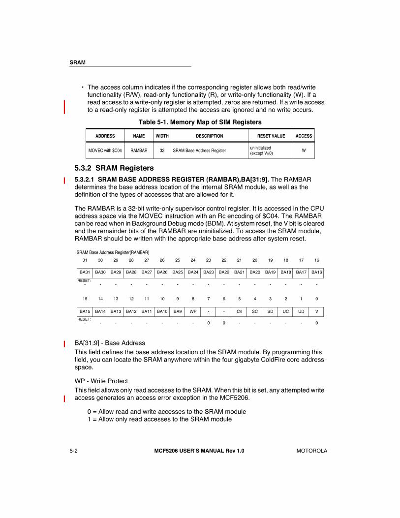
SRAM
5-2
MCF5206 USERÕS MANUAL Rev 1.0
MOTOROLA
¥ The access column indicates if the corresponding register allows both read/write functionality (R/W), read-only functionality (R), or write-only functionality (W). If a read access to a write-only register is attempted, zeros are returned. If a write access to a read-only register is attempted the access are ignored and no write occurs.
5.3.2 SRAM Registers
5.3.2.1 SRAM BASE ADDRESS REGISTER (RAMBAR),BA[31:9].
The RAMBAR determines the base address location of the internal SRAM module, as well as the definition of the types of accesses that are allowed for it.
The RAMBAR is a 32-bit write-only supervisor control register. It is accessed in the CPU address space via the MOVEC instruction with an Rc encoding of $C04. The RAMBAR can be read when in Background Debug mode (BDM). At system reset, the V bit is cleared and the remainder bits of the RAMBAR are uninitialized. To access the SRAM module, RAMBAR should be written with the appropriate base address after system reset.
BA[31:9] - Base AddressThis field defines the base address location of the SRAM module. By programming this field, you can locate the SRAM anywhere within the four gigabyte ColdFire core address space.
WP - Write ProtectThis field allows only read accesses to the SRAM. When this bit is set, any attempted write access generates an access error exception in the MCF5206.
0 = Allow read and write accesses to the SRAM module1 = Allow only read accesses to the SRAM module
Table 5-1. Memory Map of SIM Registers
ADDRESS NAME WIDTH DESCRIPTION RESET VALUE ACCESS
MOVEC with $C04 RAMBAR 32 SRAM Base Address Register uninitialized(except V=0) W
BA31 BA30 BA29 BA28 BA27 BA26 BA25 BA24 BA23 BA22 BA21 BA20 BA19 BA18 BA17 BA16
31 30 29 28 27 26 25 24 23 22 21 20 19 18 17 16
- - - - - - - - - - - - - - - -RESET:
BA15 BA14 BA13 BA12 BA11 BA10 BA9 WP - - C/I SC SD UC UD V
15 14 13 12 11 10 9 8 7 6 5 4 3 2 1 0
- - - - - - - - 0 0 - - - - - 0RESET:
SRAM Base Address Register(RAMBAR)
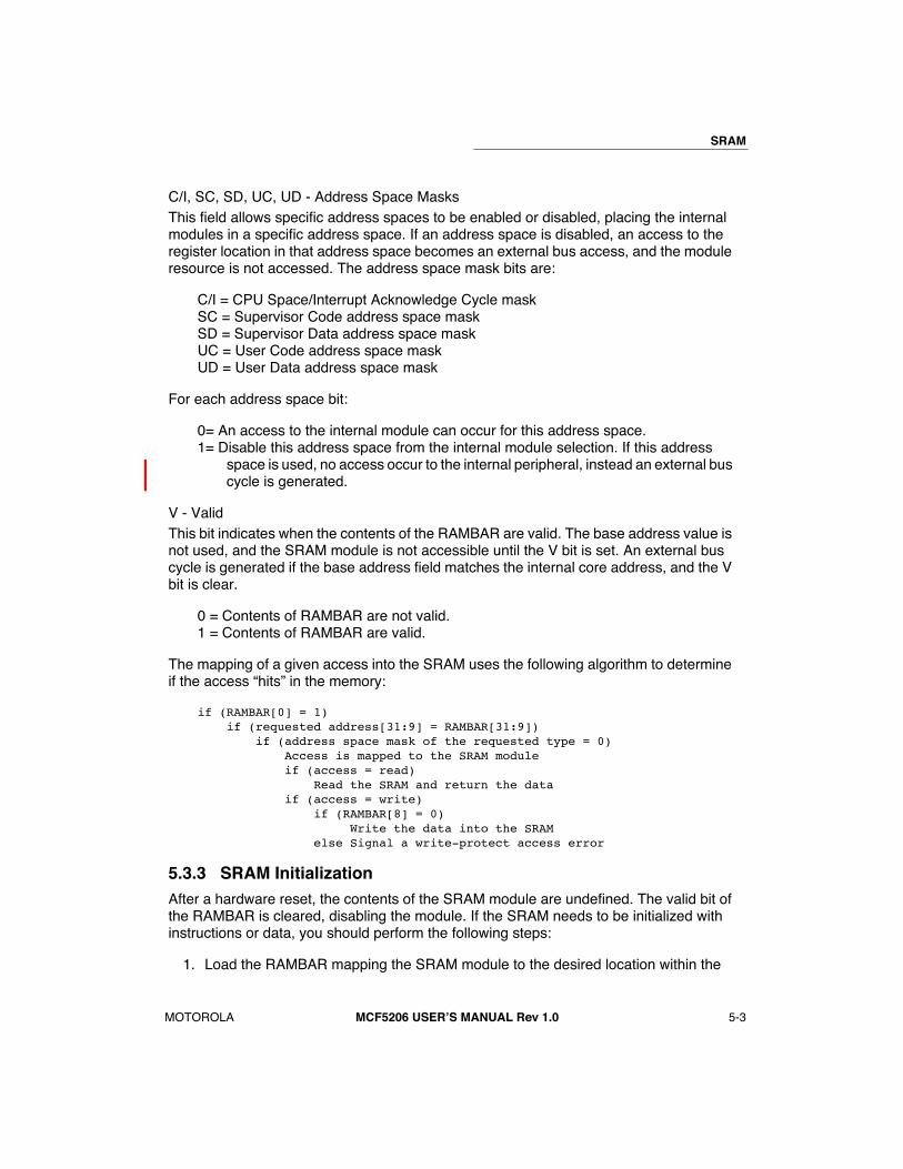
SRAM
MOTOROLA
MCF5206 USERÕS MANUAL Rev 1.0
5-3
C/I, SC, SD, UC, UD - Address Space MasksThis field allows specific address spaces to be enabled or disabled, placing the internal modules in a specific address space. If an address space is disabled, an access to the register location in that address space becomes an external bus access, and the module resource is not accessed. The address space mask bits are:
C/I = CPU Space/Interrupt Acknowledge Cycle mask SC = Supervisor Code address space maskSD = Supervisor Data address space maskUC = User Code address space maskUD = User Data address space mask
For each address space bit:
0= An access to the internal module can occur for this address space.1= Disable this address space from the internal module selection. If this address
space is used, no access occur to the internal peripheral, instead an external bus cycle is generated.
V - ValidThis bit indicates when the contents of the RAMBAR are valid. The base address value is not used, and the SRAM module is not accessible until the V bit is set. An external bus cycle is generated if the base address field matches the internal core address, and the V bit is clear.
0 = Contents of RAMBAR are not valid.1 = Contents of RAMBAR are valid.
The mapping of a given access into the SRAM uses the following algorithm to determine if the access ÒhitsÓ in the memory:
if (RAMBAR[0] = 1) if (requested address[31:9] = RAMBAR[31:9]) if (address space mask of the requested type = 0) Access is mapped to the SRAM module if (access = read) Read the SRAM and return the data if (access = write) if (RAMBAR[8] = 0) Write the data into the SRAM else Signal a write-protect access error
5.3.3 SRAM Initialization
After a hardware reset, the contents of the SRAM module are undefined. The valid bit of the RAMBAR is cleared, disabling the module. If the SRAM needs to be initialized with instructions or data, you should perform the following steps:
1. Load the RAMBAR mapping the SRAM module to the desired location within the
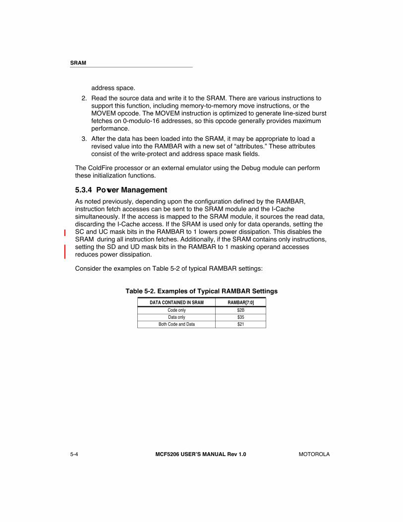
SRAM
5-4
MCF5206 USERÕS MANUAL Rev 1.0
MOTOROLA
address space.
2. Read the source data and write it to the SRAM. There are various instructions to support this function, including memory-to-memory move instructions, or the MOVEM opcode. The MOVEM instruction is optimized to generate line-sized burst fetches on 0-modulo-16 addresses, so this opcode generally provides maximum performance.
3. After the data has been loaded into the SRAM, it may be appropriate to load a revised value into the RAMBAR with a new set of Òattributes.Ó These attributes consist of the write-protect and address space mask fields.
The ColdFire processor or an external emulator using the Debug module can perform these initialization functions.
5.3.4 Power Management
As noted previously, depending upon the configuration defined by the RAMBAR, instruction fetch accesses can be sent to the SRAM module and the I-Cache simultaneously. If the access is mapped to the SRAM module, it sources the read data, discarding the I-Cache access. If the SRAM is used only for data operands, setting the SC and UC mask bits in the RAMBAR to 1 lowers power dissipation. This disables the SRAM during all instruction fetches. Additionally, if the SRAM contains only instructions, setting the SD and UD mask bits in the RAMBAR to 1 masking operand accesses reduces power dissipation.
Consider the examples on Table 5-2 of typical RAMBAR settings:
Table 5-2. Examples of Typical RAMBAR Settings
DATA CONTAINED IN SRAM RAMBAR[7:0]
Code only $2BData only $35
Both Code and Data $21
MOTOROLA
MCF5206 USERÕS MANUAL Rev 1.0
6-1
SECTION 6BUS OPERATION
The MCF5206 bus interface supports synchronous data transfers that can be terminated synchronously or asynchronously and burst or burst-inhibited between the MCF5206 and other devices in the system. This section describes the function of the bus, the signals that control the bus, and the bus cycles provided for data-transfer operations. Operation of the bus is defined for transfers initiated by the MCF5206 as a bus master and for transfers initiated by an external bus master (Note: Òexternal bus masterÓ and Òexternal bus masterÓ are used interchangeably). The section includes descriptions of the error conditions, bus arbitration, and the reset operation.
6.1 FEATURES
The following list summarizes the key bus operation features:
¥ As many as 28 bits of address and 32 bits of data
¥ Access 8-, 16-, and 32-bit port sizes
¥ Generates byte, word, longword, and line size transfers
¥ Bus arbitration for external masters
¥ Burst and burst-inhibited transfer support
¥ Internal termination generation
¥ Termination generation for external masters
6.2 BUS AND CONTROL SIGNALS
6.2.1 Address Bus (A[27:0])
These three-state bidirectional signals provide the location of a bus transfer (except for interrupt-acknowledge transfers) when the MCF5206 is the bus master. When an external bus master controls the bus, the address signals are examined when transfer start (TS) is asserted to determine if the MCF5206 should assert chip select, DRAM control, and/or transfer terminal signals . During an interrupt-acknowledge access, address lines A[27:5] are driven high, A[1:0] are driven low, and the address lines A[4:2] indicate the interrupt level being acknowledged.
DATE: 9-1-98
REVISION NO.: 1.1
PAGES AFFECTED: SEE CHANGE BARS
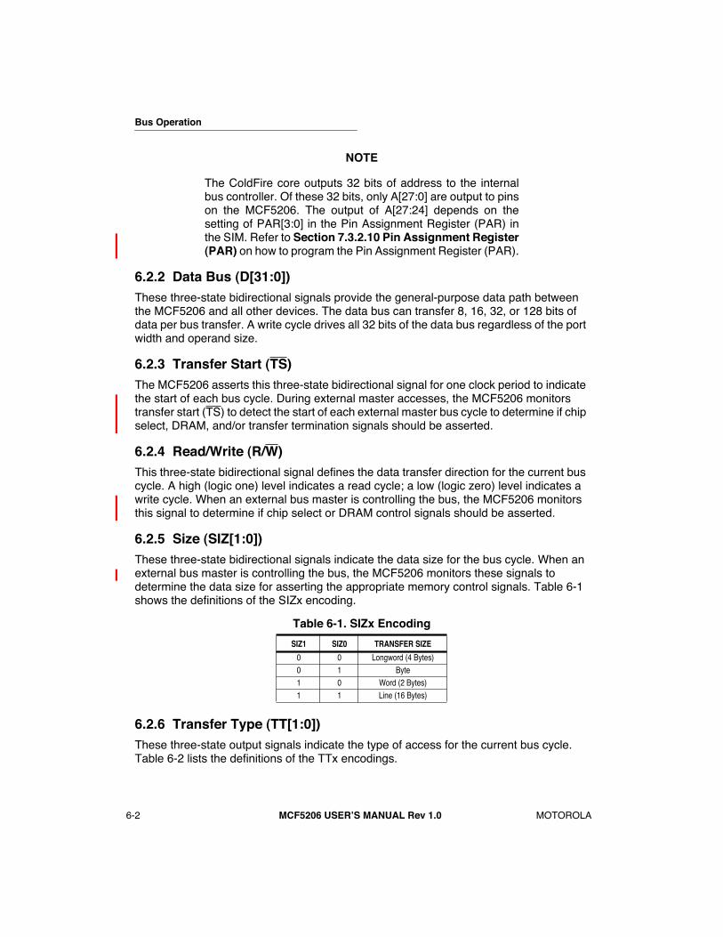
Bus Operation
6-2
MCF5206 USERÕS MANUAL Rev 1.0
MOTOROLA
NOTE
The ColdFire core outputs 32 bits of address to the internalbus controller. Of these 32 bits, only A[27:0] are output to pinson the MCF5206. The output of A[27:24] depends on thesetting of PAR[3:0] in the Pin Assignment Register (PAR) inthe SIM. Refer to
Section 7.3.2.10 Pin Assignment Register(PAR)
on how to program the Pin Assignment Register (PAR).
6.2.2 Data Bus (D[31:0])
These three-state bidirectional signals provide the general-purpose data path between the MCF5206 and all other devices. The data bus can transfer 8, 16, 32, or 128 bits of data per bus transfer. A write cycle drives all 32 bits of the data bus regardless of the port width and operand size.
6.2.3 Transfer Start (TS)
The MCF5206 asserts this three-state bidirectional signal for one clock period to indicate the start of each bus cycle. During external master accesses, the MCF5206 monitors transfer start (TS) to detect the start of each external master bus cycle to determine if chip select, DRAM, and/or transfer termination signals should be asserted.
6.2.4 Read/Write (R/W)
This three-state bidirectional signal defines the data transfer direction for the current bus cycle. A high (logic one) level indicates a read cycle; a low (logic zero) level indicates a write cycle. When an external bus master is controlling the bus, the MCF5206 monitors this signal to determine if chip select or DRAM control signals should be asserted.
6.2.5 Size (SIZ[1:0])
These three-state bidirectional signals indicate the data size for the bus cycle. When an external bus master is controlling the bus, the MCF5206 monitors these signals to determine the data size for asserting the appropriate memory control signals. Table 6-1 shows the definitions of the SIZx encoding.
6.2.6 Transfer Type (TT[1:0])
These three-state output signals indicate the type of access for the current bus cycle. Table 6-2 lists the definitions of the TTx encodings.
Table 6-1. SIZx Encoding
SIZ1 SIZ0 TRANSFER SIZE
0 0 Longword (4 Bytes)0 1 Byte1 0 Word (2 Bytes)1 1 Line (16 Bytes)

Bus Operation
MOTOROLA
MCF5206 USERÕS MANUAL Rev 1.0
6-3
The MCF5206 does not sample TT[1:0] during external master transfers.
6.2.7 Access Type and Mode (ATM)
This three-state output signal provides supplemental information for each transfer cycle type. Table 6-3 lists the encoding for normal, debug and CPU space/acknowledge transfer types.
The MCF5206 does not sample ATM during external master transfers.
6.2.8 Asynchronous Transfer Acknowledge (ATA)
This active-low asynchronous input signal indicates the successful completion of a requested data transfer operation. Asynchronous transfer acknowledge (ATA) is an input signal from the referenced slave device indicating completion of the transfer. (ATA) is synchronized internal to the MCF5206.
NOTE
The internal synchronized version of (ATA) is referred to asÒinternal asynchronous transfer acknowledge.ÕÕ Because ofthe time required to internally synchronize ATA, during a readcycle, data is latched on the rising edge of CLK when theinternal asynchronous transfer acknowledge is asserted.
Table 6-2. Transfer Type Encoding
TT1 TT0 TRANSFER TYPE
0 0 Normal Access0 1 Reserved1 0 Debug Access1 1 CPU Space/Acknowledge Access
Table 6-3. ATM Encoding
TRANSFER TYPE INTERNAL TRANSFER MODIFIER ATM (TS=0) ATM (TS=1)
00(Normal Access)
Supervisor Code 1 1Supervisor Data 0 1
User Code 1 0User Data 0 0
10(Debug Access)
Supervisor Code 1 1Supervisor Data 0 1
11(CPU Space/Acknowledge)
CPU Space - MOVEC Instruction 0 0Interrupt Acknowledge - Level 7 1 0Interrupt Acknowledge - Level 6 1 0Interrupt Acknowledge - Level 5 1 0Interrupt Acknowledge - Level 4 1 0Interrupt Acknowledge - Level 3 1 0Interrupt Acknowledge - Level 2 1 0Interrupt Acknowledge - Level 1 1 0
Bus Operation
6-4
MCF5206 USERÕS MANUAL Rev 1.0
MOTOROLA
Consequently, data must remain valid for at least one CLKcycle after the assertion of ATA. Similarly, during a write cycle,data is driven until the rising edge of CLK when the internalasynchronous transfer acknowledge is asserted.
ATA must be driven for one full clock to ensure that the MCF5206 properly synchronizes the signal. For the MCF5206 to accept the transfer as successful with an ATA, transfer error acknowledge TEA must be negated until the internal asynchronous transfer acknowledge is asserted or the transfer is completed with a bus error.
Asynchronous transfer acknowledge (ATA) is not used for termination during DRAM accesses.
6.2.9 Transfer Acknowledge (TA)
This three-state bidirectional active-low synchronous signal indicates the successful completion of a requested data transfer operation. During MCF5206-initiated transfers, transfer acknowledge (TA) is an input signal from the referenced slave device indicating completion of the transfer. For the MCF5206 to accept the transfer as successful with a transfer acknowledge, TEA must be negated throughout the transfer.
TA is not used for termination during MCF5206-initiated DRAM accesses.
When an external master is controlling the bus, the MCF5206 can drive TA to indicate the completion of the requested data transfer. If the external master-requested transfer is to a chip select or default memory, the assertion of TA is controlled by the number of wait states and the setting of the external master automatic acknowledge (EMAA) bit in the Chip Select Control Registers (CSCRs) or the Default Memory Control Register (DMCR). If the external master-requested transfer is a DRAM access, the MCF5206 drives TA as an output and is asserted at the completion of the transfer.
6.2.10 Transfer Error Acknowledge (TEA)
The external slave asserts this active-low input signal to indicate an error condition for the current transfer. The assertion of TEA immediately aborts the bus cycle. The assertion of TEA has precedence over the assertion of asynchronous transfer acknowledge (ATA) and transfer acknowledge (TA).
NOTE
TEA can be asserted up to one clock after the assertion ofasynchronous transfer acknowledge (ATA) and still berecognized.
TEA has no effect during DRAM accesses.
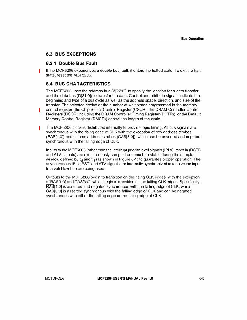
Bus Operation
MOTOROLA
MCF5206 USERÕS MANUAL Rev 1.0
6-5
6.3 BUS EXCEPTIONS
6.3.1 Double Bus Fault
If the MCF5206 experiences a double bus fault, it enters the halted state. To exit the halt state, reset the MCF5206.
6.4 BUS CHARACTERISTICS
The MCF5206 uses the address bus (A[27:0]) to specify the location for a data transfer and the data bus (D[31:0]) to transfer the data. Control and attribute signals indicate the beginning and type of a bus cycle as well as the address space, direction, and size of the transfer. The selected device or the number of wait states programmed in the memory control register (the Chip Select Control Register (CSCR), the DRAM Controller Control Registers (DCCR, including the DRAM Controller Timing Register (DCTR)), or the Default Memory Control Register (DMCR)) control the length of the cycle.
The MCF5206 clock is distributed internally to provide logic timing. All bus signals are synchronous with the rising edge of CLK with the exception of row address strobes (RAS[1:0]) and column address strobes (CAS[3:0]), which can be asserted and negated synchronous with the falling edge of CLK.
Inputs to the MCF5206 (other than the interrupt priority level signals (IPLx), reset in (RSTI) and ATA signals) are synchronously sampled and must be stable during the sample window defined by t
si
and t
hi
(as shown in Figure 6-1) to guarantee proper operation. The asynchronous IPLx, RSTI and ATA signals are internally synchronized to resolve the input to a valid level before being used.
Outputs to the MCF5206 begin to transition on the rising CLK edges, with the exception of RAS[1:0] and CAS[3:0], which begin to transition on the falling CLK edges. Specifically, RAS[1:0] is asserted and negated synchronous with the falling edge of CLK, while CAS[3:0] is asserted synchronous with the falling edge of CLK and can be negated synchronous with either the falling edge or the rising edge of CLK.
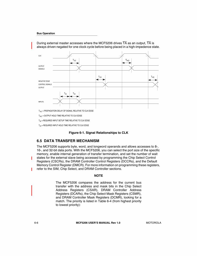
Bus Operation
6-6
MCF5206 USERÕS MANUAL Rev 1.0
MOTOROLA
During external master accesses where the MCF5206 drives TA as an output, TA is always driven negated for one clock cycle before being placed in a high-impedence state.
Figure 6-1. Signal Relationships to CLK
6.5 DATA TRANSFER MECHANISM
The MCF5206 supports byte, word, and longword operands and allows accesses to 8-, 16-, and 32-bit data ports. With the MCF5206, you can select the port size of the specific memory, enable internal generation of transfer termination, and set the number of wait states for the external slave being accessed by programming the Chip Select Control Registers (CSCRs), the DRAM Controller Control Registers (DCCRs), and the Default Memory Control Register (DMCR). For more information on programming these registers, refer to the SIM, Chip Select, and DRAM Controller sections.
NOTE
The MCF5206 compares the address for the current bustransfer with the address and mask bits in the Chip SelectAddress Registers (CSAR), DRAM Controller AddressRegisters (DCARs), the Chip Select Mask Registers (CSMR),and DRAM Controller Mask Registers (DCMR), looking for amatch. The priority is listed in Table 6-4 (from highest priorityto lowest priority):
CLK
OUTPUT
SIGNALS
INPUTS
TVO THO
TVO THO
TSI THI
TVO = PROPAGATION DELAY OF SIGNAL RELATIVE TO CLK EDGE
THO = OUTPUT HOLD TIME RELATIVE TO CLK EDGE
TSI = REQUIRED INPUT SETUP TIME RELATIVE TO CLK EDGE
THI = REQUIRED INPUT HOLD TIME RELATIVE TO CLK EDGE
NEGATIVE EDGE
CONTROL SIGNALS
OUTPUT
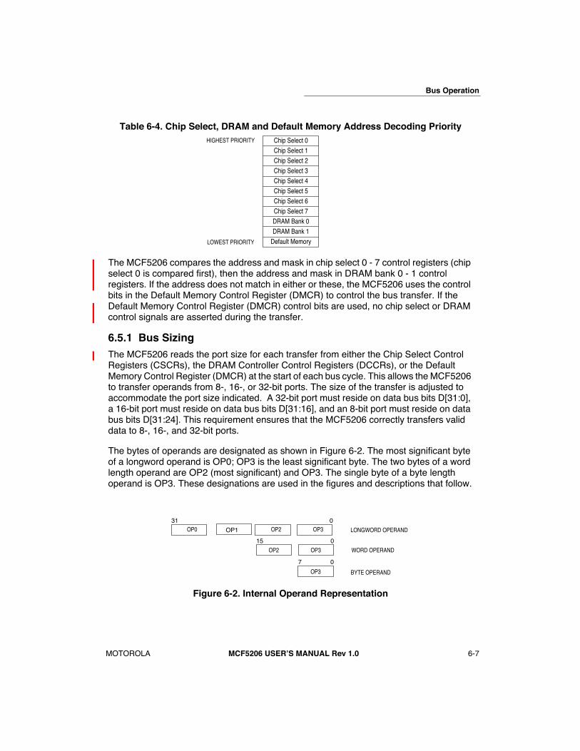
Bus Operation
MOTOROLA
MCF5206 USERÕS MANUAL Rev 1.0
6-7
The MCF5206 compares the address and mask in chip select 0 - 7 control registers (chip select 0 is compared first), then the address and mask in DRAM bank 0 - 1 control registers. If the address does not match in either or these, the MCF5206 uses the control bits in the Default Memory Control Register (DMCR) to control the bus transfer. If the Default Memory Control Register (DMCR) control bits are used, no chip select or DRAM control signals are asserted during the transfer.
6.5.1 Bus Sizing
The MCF5206 reads the port size for each transfer from either the Chip Select Control Registers (CSCRs), the DRAM Controller Control Registers (DCCRs), or the Default Memory Control Register (DMCR) at the start of each bus cycle. This allows the MCF5206 to transfer operands from 8-, 16-, or 32-bit ports. The size of the transfer is adjusted to accommodate the port size indicated. A 32-bit port must reside on data bus bits D[31:0], a 16-bit port must reside on data bus bits D[31:16], and an 8-bit port must reside on data bus bits D[31:24]. This requirement ensures that the MCF5206 correctly transfers valid data to 8-, 16-, and 32-bit ports.
The bytes of operands are designated as shown in Figure 6-2. The most significant byte of a longword operand is OP0; OP3 is the least significant byte. The two bytes of a word length operand are OP2 (most significant) and OP3. The single byte of a byte length operand is OP3. These designations are used in the figures and descriptions that follow.
Figure 6-2. Internal Operand Representation
Table 6-4. Chip Select, DRAM and Default Memory Address Decoding Priority
Chip Select 0Chip Select 1Chip Select 2Chip Select 3Chip Select 4Chip Select 5Chip Select 6Chip Select 7DRAM Bank 0DRAM Bank 1
Default Memory
LONGWORD OPERAND
WORD OPERAND
BYTE OPERAND
31 0
15 0
7 0
OP3
OP3
OP3
OP2
OP2OP0 OP1
HIGHEST PRIORITY
LOWEST PRIORITY

Bus Operation
6-8
MCF5206 USERÕS MANUAL Rev 1.0
MOTOROLA
Figure 6-3 shows the required organization of data ports on the MCF5206 for 8-, 16-, and 32 bit devices. The four bytes shown are connected through the internal data bus and data multiplexer to the external data bus. This path is how the MCF5206 supports programmable port sizing and operand misalignment. The data multiplexer establishes the necessary connections for different combinations of address and data sizes.
Figure 6-3. MCF5206 Interface to Various Port Sizes
The multiplexer takes the four bytes of the 32-bit bus and routes them to their required positions. For example, OP3 can be routed to D[7:0], as would be the normal case when interfacing to a 32-bit port. OP3 can be routed to D[23:16] for interfacing to a 16-bit port, or it can be routed to D[31:24] for interfacing to an 8-bit port. The operand size, address, and port size of the memory being accessed determines the positioning of bytes.
The MCF5206 can burst anytime the port size of the external slave being accessed is smaller than the operand size. If bursting is enabled, the MCF5206 burst transfers depending on the port size and operand alignment. For any transfer, the number of bytes transferred during a bus cycle is equal to or less than the size indicated by the SIZx outputs. For example, during the first bus cycle of a longword transfer to a 16-bit port where bursting is enabled, the SIZx outputs remain constant throughout the transfer and indicate that four bytes are to be transferred, although only two bytes are moved at a time.Table 6-5 lists the encodings for the SIZx bits for each port size for transfers where bursting is both enabled and disabled.
A[0] and A[1] also affect operation of the data multiplexer. During an operand transfer, A[31:2] indicate the longword base address of that portion of the operand to be accessed; A[1] and A[0] indicate the byte offset from the base. Table 6-6 lists the encoding of A[1] and A[0] and the corresponding byte offset from the longword base.
REGISTER
MULTIPLEXER
EXTERNAL
DATA BUS
ADDRESS
BYTE 0
INTERNAL TO
MCF5206
8-BIT PORT
16-BIT PORT
32-BIT PORT
BYTE 1
BYTE 2
BYTE 3
BYTE 0 BYTE 1
BYTE 2 BYTE 3
BYTE 0 BYTE 1 BYTE 2 BYTE 3
D[31:24] D[23:16] D[15:8] D[7:0]
ROUTING AND DUPLICATION
OP0 OP1 OP2 OP3
A1 A0
0 0
0 0
1 0
0 0
0 1
1 0
1 1

Bus Operation
MOTOROLA
MCF5206 USERÕS MANUAL Rev 1.0
6-9
Table 6-7 lists the bytes that should be driven on the data bus during read cycles by the slave device being accessed. The entries shown as Byte X are portions of the requested operand that are read. The operand being read is defined by SIZ[1], SIZ[0], A[0], and A[1] for the bus cycle. Bytes labeled X are ÒdonÕt caresÓ and are not required during that read cycle. Bytes labeled Ò-Ó indicates that this transfer is not valid.
Table 6-5. SIZx Encoding for Burst- and Bursting-Inhibited Ports
OPERANDSIZE
32-BIT PORT 16 -BIT PORT 8-BIT PORT
BURSTING ENABLED
BURSTING INHIBITED
BURSTINGENABLED
BURSTINGINHIBITED
BURSTINGENABLED
BURSTINGINHIBITED
SIZ1 SIZ0 SIZ1 SIZ0 SIZ1 SIZ0 SIZ1 SIZ0 SIZ1 SIZ0 SIZ1 SIZ0
BYTE 0 1 0 1 0 1 0 1 0 1 0 1
WORD 1 0 1 0 1 0 1 0 1 0 0 1
LONGWORD 0 0 0 0 0 0 1 0 0 0 0 1
LINE 1 1 0 0 1 1 1 0 1 1 0 1
Table 6-6. Address Offset Encoding
A1 A0 OFFSET
0 0 +0 Byte0 1 +1 Byte1 0 +2 Bytes1 1 +3 Bytes
Table 6-7. Data Bus Requirement for Read Cycles
TRANSFER SIZE
SIZE ADDRESS32 BIT PORT
EXTERNAL DATA BYTES REQUIRED
16 BIT PORTEXTERNAL DATABYTES REQUIRED
8 BIT PORTEXTERNAL DATA BYTES REQUIRED
SIZ1 SIZ0 A1 A0 D[31:24] D[23:16] D[15:8] D[7:0] D[31:24] D[23:16] D[31:24]
BYTE
0 1
0 0 Byte 0 X X X Byte 0 X Byte 0
0 1 X Byte 1 X X X Byte 1 Byte 1
1 0 X X Byte 2 X Byte 2 X Byte 2
1 1 X X X Byte 3 X Byte 3 Byte 3
WORD
1 0
0 0 Byte 0 Byte 1 X X Byte 0 Byte 1 Byte 0
0 1 - - - - - - Byte 1
1 0 X X Byte2 Byte 3 Byte 2 Byte 3 Byte 2
1 1 - - - - - - Byte 3
LONGWORD
0 0
0 0 Byte 0 Byte 1 Byte 2 Byte 3 Byte 0 Byte 1 Byte 0
0 1 - - - - - - Byte 1
1 0 - - - - Byte 2 Byte 3 Byte 2
1 1 - - - - - - Byte 3

Bus Operation
6-10
MCF5206 USERÕS MANUAL Rev 1.0
MOTOROLA
Figure 6-4 is a flowchart for read transfers to 8-, 16-, or 32-bit ports. Bus operations are similar for each case and vary only with the size indicated, the portion of the data bus used for the transfer, and the specific number of cycles needed for each transfer.
Figure 6-4. Byte-, Word-, and Longword-Read Transfer Flowchart
LINE
1 1
0 0 Byte 0 Byte 1 Byte 2 Byte 3 Byte 0 Byte 1 Byte 0
0 1 - - - - - - Byte 1
1 0 - - - - Byte 2 Byte 3 Byte 2
1 1 - - - - - - Byte 3
Table 6-7. Data Bus Requirement for Read Cycles (Continued)
TRANSFER SIZE
SIZE ADDRESS32 BIT PORT
EXTERNAL DATA BYTES REQUIRED
16 BIT PORTEXTERNAL DATABYTES REQUIRED
8 BIT PORTEXTERNAL DATA BYTES REQUIRED
SIZ1 SIZ0 A1 A0 D[31:24] D[23:16] D[15:8] D[7:0] D[31:24] D[23:16] D[31:24]
MCF5206 SYSTEM
1. DRIVE ADDRESS ON A[27:0]
2. DRIVE R/W TO READ (R/W = 1)
3. DRIVE SIZ[1:0] TO INDICATE BYTE, WORD OR LONGWORD
4. DRIVE TT[1:0] AND ATM TO INDICATE APPROPRIATE ACCESS TYPE
5. ASSERT TS FOR ONE CLK CYCLE
1. DECODE ADDRESS AND SELECT THE APPROPRIATE SLAVE DEVICE.*
2. DRIVE DATA ON APPROPRIATE BYTE LANES BASED ON SIZ[1:0], A[1:0] AND PORT SIZE
3. ASSERT TA FOR ONE CLK CYCLE
1. NEGATE TS
2. DRIVE ATM TO INDICATE APPROPRIATE ACCESS TYPEAND MODE
1. REGISTER DATA
2. RECOGNIZE THE TRANSFER IS DONE
*TO INSERT WAIT STATES, T A IS DRIVEN NEGATED.
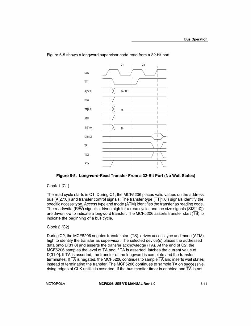
Bus Operation
MOTOROLA
MCF5206 USERÕS MANUAL Rev 1.0
6-11
Figure 6-5 shows a longword supervisor code read from a 32-bit port.
Figure 6-5. Longword-Read Transfer From a 32-Bit Port (No Wait States)
Clock 1 (C1)
The read cycle starts in C1. During C1, the MCF5206 places valid values on the address bus (A[27:0]) and transfer control signals. The transfer type (TT[1:0]) signals identify the specific access type. Access type and mode (ATM) identifies the transfer as reading code. The read/write (R/W) signal is driven high for a read cycle, and the size signals (SIZ[1:0]) are driven low to indicate a longword transfer. The MCF5206 asserts transfer start (TS) to indicate the beginning of a bus cycle.
Clock 2 (C2)
During C2, the MCF5206 negates transfer start (TS), drives access type and mode (ATM) high to identify the transfer as supervisor. The selected device(s) places the addressed data onto D[31:0] and asserts the transfer acknowledge (TA). At the end of C2, the MCF5206 samples the level of TA and if TA is asserted, latches the current value of D[31:0]. If TA is asserted, the transfer of the longword is complete and the transfer terminates. If TA is negated, the MCF5206 continues to sample TA and inserts wait states instead of terminating the transfer. The MCF5206 continues to sample TA on successive rising edges of CLK until it is asserted. If the bus monitor timer is enabled and TA is not
TS
A[27:0]
R/W
CLK
TT[1:0]
ATM
TA
D[31:0]
TEA
SIZ[1:0]
C1 C2
$0
$0
$ADDR
ATA

Bus Operation
6-12
MCF5206 USERÕS MANUAL Rev 1.0
MOTOROLA
asserted before the programmed bus monitor time is reached, the cycle is terminated with an internal bus error.
Table 6-8 lists the combinations of SIZ[1:0], A[1:0] and the corresponding pattern of the data transfer for write cycles from the internal multiplexer of the MCF5206 to the external data bus. For example, if a longword transfer is generated to a 16-bit port, the MCF5206 starts the cycle with A[1:0] set to $0 and read the first word. The MCF5206 then increments A[1:0] to $2 and reads the second word. The data for both word reads is sampled from DATA[31:16]. Bytes labeled X are ÒdonÕt cares.Ó
Table 6-8. Internal to External Data Bus Multiplexer - Write Cycle
TRANSFER SIZE
SIZE ADDRESS EXTERNAL DATA BUS CONNECTION
SIZ1 SIZ0 A1 A0 D[31:24] D[23:16] D[15:8] D[7:0]
BYTE
0 1 0 0 OP3 X X X0 1 OP3 OP3 X X1 0 OP3 X OP3 X1 1 OP3 OP3 X OP3
WORD
1 0 0 0 OP2 OP3 X X0 1 OP3 X X X1 0 OP2 OP3 OP2 OP31 1 OP3 X X X
LONGWORD
0 0 0 0 OP0 OP1 OP2 OP30 1 OP1 X X X1 0 OP2 OP3 X X1 1 OP3 X X X
LINE
1 1 0 0 OP0 OP1 OP2 OP30 1 OP1 X X X1 0 OP2 OP3 X X1 1 OP3 X X X

Bus Operation
MOTOROLA
MCF5206 USERÕS MANUAL Rev 1.0
6-13
Figure 6-6 is a flowchart for write transfers to 8-, 16-, or 32-bit ports. Bus operations are similar for each case and vary only with the size indicated, the portion of the data bus used for the transfer and the specific number of cycles needed for each transfer.
Figure 6-6. Byte-, Word-, and Longword-Write Transfer Flowchart
MCF5206 SYSTEM
1. DRIVE ADDRESS ON A[27:0]
2. DRIVE R/W TO WRITE (R/W = 0)
3. DRIVE SIZ[1:0] TO INDICATE BYTE, WORD OR LONGWORD
4. DRIVE TT[1:0] AND ATM TO INDICATE APPROPRIATE ACCESS TYPE
5. ASSERT TS FOR ONE CLK CYCLE
1. NEGATE TS
2. DRIVE ATM TO INDICATE APPROPRIATE ACCESS TYPE
3. DRIVE DATA ON APPROPRIATE BYTE LANES BASED ON SIZ[1:0], A[1:0] AND PORT SIZE
1. RECOGNIZE THE TRANSFER IS DONE
2. THREE-STATE D[31:0]
1. DECODE ADDRESS AND SELECT THE APPROPRIATE SLAVE DEVICE.*
2. CAPTURE DATA FROM THE APPROPRIATE BYTE LANES BASED ON SIZ[1:0], A[1:0] AND PORT SIZE
3. ASSERT TA FOR ONE CLK CYCLE
*TO INSERT WAIT STATES, TA IS DRIVEN NEGATED.
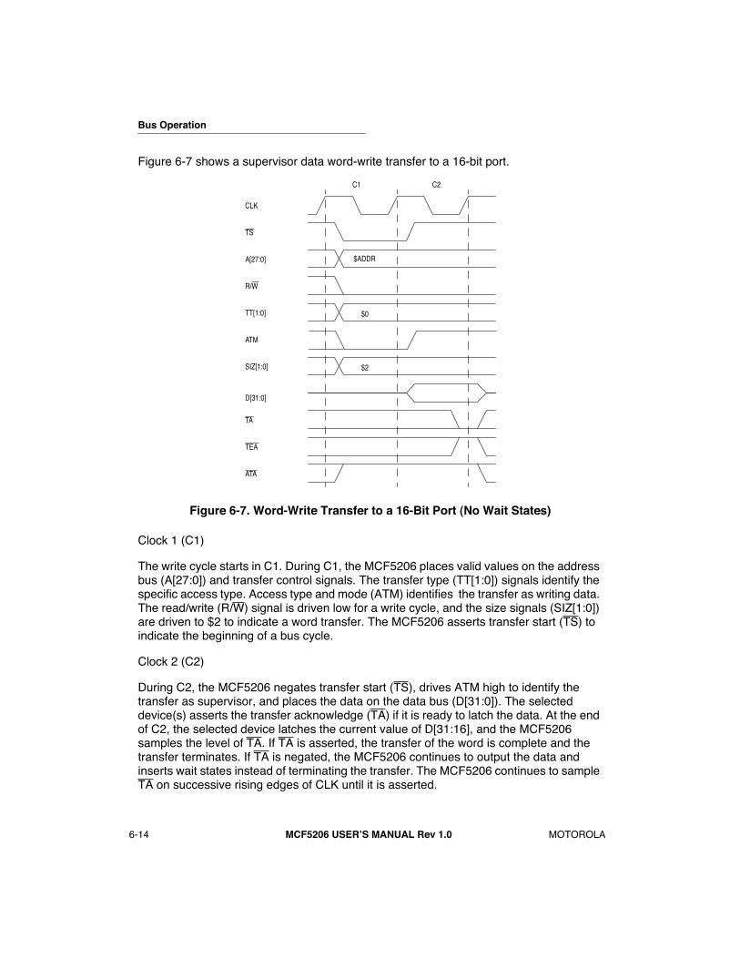
Bus Operation
6-14
MCF5206 USERÕS MANUAL Rev 1.0
MOTOROLA
Figure 6-7 shows a supervisor data word-write transfer to a 16-bit port.
Figure 6-7. Word-Write Transfer to a 16-Bit Port (No Wait States)
Clock 1 (C1)
The write cycle starts in C1. During C1, the MCF5206 places valid values on the address bus (A[27:0]) and transfer control signals. The transfer type (TT[1:0]) signals identify the specific access type. Access type and mode (ATM) identifies the transfer as writing data. The read/write (R/W) signal is driven low for a write cycle, and the size signals (SIZ[1:0]) are driven to $2 to indicate a word transfer. The MCF5206 asserts transfer start (TS) to indicate the beginning of a bus cycle.
Clock 2 (C2)
During C2, the MCF5206 negates transfer start (TS), drives ATM high to identify the transfer as supervisor, and places the data on the data bus (D[31:0]). The selected device(s) asserts the transfer acknowledge (TA) if it is ready to latch the data. At the end of C2, the selected device latches the current value of D[31:16], and the MCF5206 samples the level of TA. If TA is asserted, the transfer of the word is complete and the transfer terminates. If TA is negated, the MCF5206 continues to output the data and inserts wait states instead of terminating the transfer. The MCF5206 continues to sample TA on successive rising edges of CLK until it is asserted.
TS
A[27:0]
R/W
CLK
TT[1:0]
ATM
TA
D[31:0]
TEA
SIZ[1:0]
C1 C2
$2
$0
ATA
$ADDR
Bus Operation
MOTOROLA
MCF5206 USERÕS MANUAL Rev 1.0
6-15
6.5.2 Bursting Read Transfers: Word, Longword, and Line
If the burst-enable bit in the appropriate control register (Chip Select Control Register or Default Memory Control Register) is set to 1or the transfer is to DRAM, and the operand size is larger than the port size of the memory being accessed, the MCF5206 performs word, longword, and line transfers in burst mode. When burst mode is selected, the size of the transfer (indicated by SIZ[1:0]) reflects the size of the operand being read, not the size of the port being accessed (i.e., a line transfer is indicated by SIZ[1:0] = $3 and a longword transfer is indicated by SIZ[1:0] = $0, regardless of the size of the port or the number of transfers required to access the entire set of data).
The MCF5206 supports burst-inhibited transfers for memory devices that cannot support bursting. For this type of bus cycle, you should clear the burst-enable bit in the Chip Select Control Registers (CSCRs) or Default Memory Control Register (DMCR).
NOTE
No burst-enable bit is provided for DRAM accesses. DRAMtransfers are always bursted if the operand size is larger thanthe port size.
The MCF5206 uses line read transfers to access a 16-byte operand to support cache line filling and for a MOVEM instruction, when appropriate. A line read accesses a block of four longwords, aligned to a longword memory boundary, by supplying a starting address that points to one of the longwords and incrementing A3, A2, A1, and A0 of the supplied address for each transfer. A longword read accesses a single longword aligned to a longword boundary and increments A1 and A0 if the accessed port size is smaller than 32 bits. A word read accesses a single word of data, aligned to a word boundary and increments A0 if the accessed port size is smaller than 16 bits.
Figure 6-8 is a flowchart for bursting read transfers to 8-, 16-, or 32-bit ports. Bus operations are similar for each case and vary only with the size indicated, the portion of the data bus used for the transfer, and the specific number of cycles needed for each
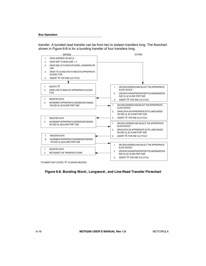
Bus Operation
6-16
MCF5206 USERÕS MANUAL Rev 1.0
MOTOROLA
transfer. A bursted read transfer can be from two to sixteen transfers long. The flowchart shown in Figure 6-8 is for a bursting transfer of four transfers long.
Figure 6-8. Bursting Word-, Longword-, and Line-Read Transfer Flowchart
MCF5206 SYSTEM
1. DRIVE ADDRESS ON A[27:0]
2. DRIVE R/W TO READ (R/W = 1)
3. DRIVE SIZ[1:0] TO INDICATE WORD, LONGWORD OR LINE
4. DRIVE TT[1:0] AND ATM TO INDICATE APPROPRIATE ACCESS TYPE
5. ASSERT TS FOR ONE CLK CYCLE
1. NEGATE TS
2. DRIVE ATM TO INDICATE APPROPRIATE ACCESS TYPE
1. REGISTER DATA
2. RECOGNIZE THE TRANSFER IS DONE
1. REGISTER DATA
2. INCREMENT APPROPRIATE ADDRESS BITS BASED ON SIZ[1:0], A[3:0] AND PORT SIZE
1. REGISTER DATA
2. INCREMENT APPROPRIATE ADDRESS BITS BASED ON SIZ[1:0], A[3:0] AND PORT SIZE
1. REGISTER DATA
2. INCREMENT APPROPRIATE ADDRESS BITS BASED ON SIZ[1:0], A[3:0] AND PORT SIZE
1. DECODE ADDRESS AND SELECT THE APPROPRIATE SLAVE DEVICE*
2. DRIVE DATA ON APPROPRIATE BYTE LANES BASED ON SIZ[1:0], A[1:0] AND PORT SIZE
3. ASSERT TA FOR ONE CLK CYCLE
1. DECODE ADDRESS AND SELECT THE APPROPRIATE SLAVE DEVICE.*
2. DRIVE DATA ON APPROPRIATE BYTE LANES BASED ON SIZ[1:0], A[1:0] AND PORT SIZE
3. ASSERT TA FOR ONE CLK CYCLE
*TO INSERT WAIT STATES, TA IS DRIVEN NEGATED.
1. DECODE ADDRESS AND SELECT THE APPROPRIATE SLAVE DEVICE.*
2. DRIVE DATA ON APPROPRIATE BYTE LANES BASED ON SIZ[1:0], A[1:0] AND PORT SIZE
3. ASSERT TA FOR ONE CLK CYCLE
1. DECODE ADDRESS AND SELECT THE APPROPRIATE SLAVE DEVICE.*
2. DRIVE DATA ON APPROPRIATE BYTE LANES BASED ON SIZ[1:0], A[1:0] AND PORT SIZE
3. ASSERT TA FOR ONE CLK CYCLE
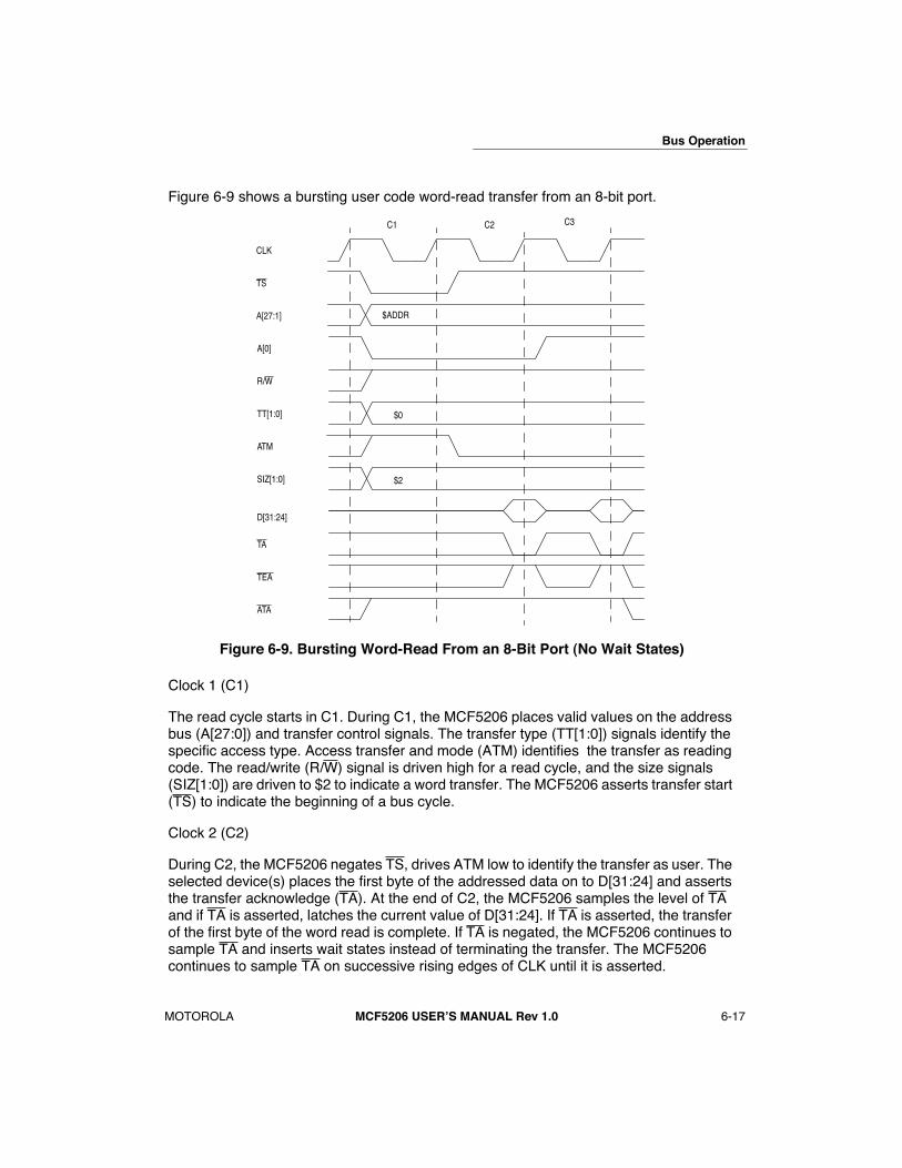
Bus Operation
MOTOROLA
MCF5206 USERÕS MANUAL Rev 1.0
6-17
Figure 6-9 shows a bursting user code word-read transfer from an 8-bit port.
Figure 6-9. Bursting Word-Read From an 8-Bit Port (No Wait States)
Clock 1 (C1)
The read cycle starts in C1. During C1, the MCF5206 places valid values on the address bus (A[27:0]) and transfer control signals. The transfer type (TT[1:0]) signals identify the specific access type. Access transfer and mode (ATM) identifies the transfer as reading code. The read/write (R/W) signal is driven high for a read cycle, and the size signals (SIZ[1:0]) are driven to $2 to indicate a word transfer. The MCF5206 asserts transfer start (TS) to indicate the beginning of a bus cycle.
Clock 2 (C2)
During C2, the MCF5206 negates TS, drives ATM low to identify the transfer as user. The selected device(s) places the first byte of the addressed data on to D[31:24] and asserts the transfer acknowledge (TA). At the end of C2, the MCF5206 samples the level of TA and if TA is asserted, latches the current value of D[31:24]. If TA is asserted, the transfer of the first byte of the word read is complete. If TA is negated, the MCF5206 continues to sample TA and inserts wait states instead of terminating the transfer. The MCF5206 continues to sample TA on successive rising edges of CLK until it is asserted.
TS
A[27:1]
R/W
CLK
TT[1:0]
ATM
TA
D[31:24]
TEA
SIZ[1:0]
C1 C2
$2
$0
C3
$ADDR
A[0]
ATA
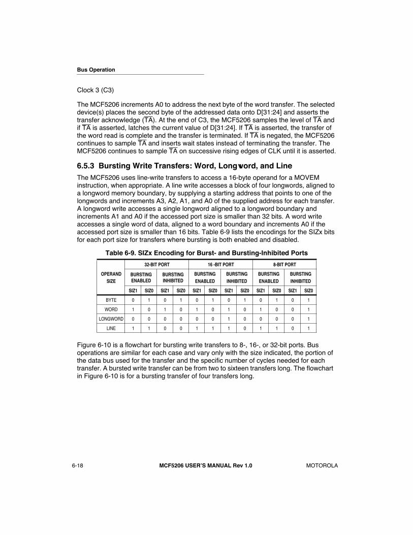
Bus Operation
6-18
MCF5206 USERÕS MANUAL Rev 1.0
MOTOROLA
Clock 3 (C3)
The MCF5206 increments A0 to address the next byte of the word transfer. The selected device(s) places the second byte of the addressed data onto D[31:24] and asserts the transfer acknowledge (TA). At the end of C3, the MCF5206 samples the level of TA and if TA is asserted, latches the current value of D[31:24]. If TA is asserted, the transfer of the word read is complete and the transfer is terminated. If TA is negated, the MCF5206 continues to sample TA and inserts wait states instead of terminating the transfer. The MCF5206 continues to sample TA on successive rising edges of CLK until it is asserted.
6.5.3 Bursting Write Transfers: Word, Longword, and Line
The MCF5206 uses line-write transfers to access a 16-byte operand for a MOVEM instruction, when appropriate. A line write accesses a block of four longwords, aligned to a longword memory boundary, by supplying a starting address that points to one of the longwords and increments A3, A2, A1, and A0 of the supplied address for each transfer. A longword write accesses a single longword aligned to a longword boundary and increments A1 and A0 if the accessed port size is smaller than 32 bits. A word write accesses a single word of data, aligned to a word boundary and increments A0 if the accessed port size is smaller than 16 bits. Table 6-9 lists the encodings for the SIZx bits for each port size for transfers where bursting is both enabled and disabled.
Figure 6-10 is a flowchart for bursting write transfers to 8-, 16-, or 32-bit ports. Bus operations are similar for each case and vary only with the size indicated, the portion of the data bus used for the transfer and the specific number of cycles needed for each transfer. A bursted write transfer can be from two to sixteen transfers long. The flowchart in Figure 6-10 is for a bursting transfer of four transfers long.
Table 6-9. SIZx Encoding for Burst- and Bursting-Inhibited Ports
OPERANDSIZE
32-BIT PORT 16 -BIT PORT 8-BIT PORT
BURSTING ENABLED
BURSTING INHIBITED
BURSTINGENABLED
BURSTINGINHIBITED
BURSTINGENABLED
BURSTINGINHIBITED
SIZ1 SIZ0 SIZ1 SIZ0 SIZ1 SIZ0 SIZ1 SIZ0 SIZ1 SIZ0 SIZ1 SIZ0
BYTE 0 1 0 1 0 1 0 1 0 1 0 1
WORD 1 0 1 0 1 0 1 0 1 0 0 1
LONGWORD 0 0 0 0 0 0 1 0 0 0 0 1
LINE 1 1 0 0 1 1 1 0 1 1 0 1
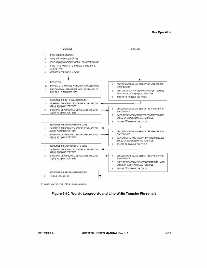
Bus Operation
MOTOROLA
MCF5206 USERÕS MANUAL Rev 1.0
6-19
Figure 6-10. Word-, Longword-, and Line-Write Transfer Flowchart
MCF5206 SYSTEM
1. DRIVE ADDRESS ON A[27:0]
2. DRIVE R/W TO WRITE (R/W = 0)
3. DRIVE SIZ[1:0] TO INDICATE WORD, LONGWORD OR LINE
4. DRIVE TT[1:0] AND ATM TO INDICATE APPROPRIATE ACCESS TYPE
5. ASSERT TS FOR ONE CLK CYCLE
1. RECOGNIZE THE 4TH TRANSFER IS DONE
2. THREE-STATE D[31:0]
1. RECOGNIZE THE 2ND TRANSFER IS DONE
2. INCREMENT APPROPRIATE ADDRESS BITS BASED ON SIZ[1:0], A[3:0] AND PORT SIZE
3. DRIVE DATA ON APPROPRIATE BYTE LANES BASED ON SIZ[1:0], A[1:0] AND PORT SIZE
*TO INSERT WAIT STATES, TA IS DRIVEN NEGATED .
1. DECODE ADDRESS AND SELECT THE APPROPRIATE SLAVE DEVICE.*
2. CAPTURE DATA FROM THE APPROPRIATE BYTE LANES BASED ON SIZ[1:0], A[1:0] AND PORT SIZE
3. ASSERT TA FOR ONE CLK CYCLE
1. DECODE ADDRESS AND SELECT THE APPROPRIATE SLAVE DEVICE.*
2. CAPTURE DATA FROM THE APPROPRIATE BYTE LANES BASED ON SIZ[1:0], A[1:0] AND PORT SIZE
3. ASSERT TA FOR ONE CLK CYCLE
1. DECODE ADDRESS AND SELECT THE APPROPRIATE SLAVE DEVICE.*
2. CAPTURE DATA FROM THE APPROPRIATE BYTE LANES BASED ON SIZ[1:0], A[1:0] AND PORT SIZE
3. ASSERT TA FOR ONE CLK CYCLE
1. DECODE ADDRESS AND SELECT THE APPROPRIATE SLAVE DEVICE.*
2. CAPTURE DATA FROM THE APPROPRIATE BYTE LANES BASED ON SIZ[1:0], A[1:0] AND PORT SIZE
3. ASSERT TA FOR ONE CLK CYCLE
1. RECOGNIZE THE 3RD TRANSFER IS DONE
2. INCREMENT APPROPRIATE ADDRESS BITS BASED ON SIZ[1:0], A[3:0] AND PORT SIZE
3. DRIVE DATA ON APPROPRIATE BYTE LANES BASED ON SIZ[1:0], A[1:0] AND PORT SIZE
1. NEGATE TS
2. DRIVE ATM TO INDICATE APPROPRIATE ACCESS TYPE
3. DRIVE DATA ON APPROPRIATE BYTE LANES BASED ON SIZ[1:0], A[1:0] AND PORT SIZE
1. RECOGNIZE THE 1ST TRANSFER IS DONE
2. INCREMENT APPROPRIATE ADDRESS BITS BASED ON SIZ[1:0], A[3:0] AND PORT SIZE
3. DRIVE DATA ON APPROPRIATE BYTE LANES BASED ON SIZ[1:0], A[1:0] AND PORT SIZE

Bus Operation
6-20
MCF5206 USERÕS MANUAL Rev 1.0
MOTOROLA
Figure 6-11 shows a user data bursting line-write transfer to a 32-bit port.
Figure 6-11. Line-Write Transfer to a 32-Bit Port (No Wait States)
Clock 1 (C1)
The write cycle starts in C1. During C1, the MCF5206 places valid values on the address bus (A[27:0]) and transfer control signals. The transfer type (TT[1:0]) signals identify the specific access type. Access type and mode (ATM) identifies the transfer as data. The read/write (R/W) signal is driven low for a write cycle, and the size signals (SIZ[1:0]) are driven to $3 to indicate a line transfer. The MCF5206 asserts transfer start (TS) to indicate the beginning of a bus cycle.
Clock 2 (C2)
During C2, the MCF5206 negates TS, drives ATM low to identify the transfer as user, and places the data on the data bus (D[31:0]). The selected device(s) asserts the transfer acknowledge (TA) if it is ready to latch the data. At the end of C2, the selected device latches the current value of D[31:0], and the MCF5206 samples the level of TA. If TA is asserted, the transfer of the first longword is complete. If TA is negated, the MCF5206
TS
A[27:4]
R/W
CLK
TT[1:0]
ATM
TA
D[31:0]
TEA
SIZ[1:0]
C1 C2
$3
$0
C3 C4
$ADDR
C5
A[3:2] $2 $3 $0 $1
A[1:0]
ATA

Bus Operation
MOTOROLA
MCF5206 USERÕS MANUAL Rev 1.0
6-21
continues to output the data and inserts wait states instead of terminating the transfer. The MCF5206 continues to sample TA on successive rising edges of CLK until it is asserted.
Clock 3 (C3)
The MCF5206 increments A[3:2] to address the next longword of the line transfer and drives D[31:0] with the second longword of data. The selected device(s) asserts the TA if it is ready to latch the data. At the end of C3, the MCF5206 samples the level of TA and if TA is asserted, the second longword transfer of the line write is complete. If TA is negated, the MCF5206 continues to sample TA and inserts wait states instead of terminating the transfer. The MCF5206 continues to sample TA on successive rising edges of CLK until it is asserted.
Clock 4 (C4)
This clock is identical to C3, except that once TA is asserted, the value corresponds to the third longword of data for the burst.
Clock 5 (C5)
This clock is identical to C3, except that once TA is asserted, the data value corresponds to the fourth longword of data for the burst. This is the last CLK cycle of the line-write transfer and the MCF5206 three-states D[31:0] at the start of the next CLK cycle.
6.5.4 Burst-Inhibited Read Transfer: Word, Longword, and Line
If the burst-enable bit in the appropriate control register (Chip Select Control Register or Default Memory Control Register) is cleared and the operand size is larger than the port size of the memory being accessed, the MCF5206 performs word, longword, and line transfers in burst-inhibited mode. When burst-inhibit mode is selected, the size of the transfer (indicated by SIZ[1:0]) reflects the port size if the operand being read is larger than the port size or the operand size if the port size is larger than the operand size. A transfer size of line (SIZ[1:0] = $3) is never indicated in burst-inhibited mode. If the operand size is line, the size pins (SIZ[1:0]) always indicates the port size. Refer to Table 6-9 for SIZx encodings for each port size for burst-inhibited transfers.
NOTE
All transfers to DRAM that have an operand size larger thanthe port size are bursted. Burst-inhibited transfers cannot begenerated for DRAM accesses.
The basic transfer of a burst-inhibited read is the same as a ÒnormalÓ read with the addition of more transfers until the entire operand has been accessed. Burst-inhibited read transfers can be from two to sixteen transfers long. Figure 6-12 is a flowchart for burst-inhibited read transfers (4 transfers long) to 8-, 16-, or 32-bit ports. Bus operations are similar for each case and vary only with the size indicated, the portion of the data bus used for the transfer, and the specific number of cycles needed for each transfer.
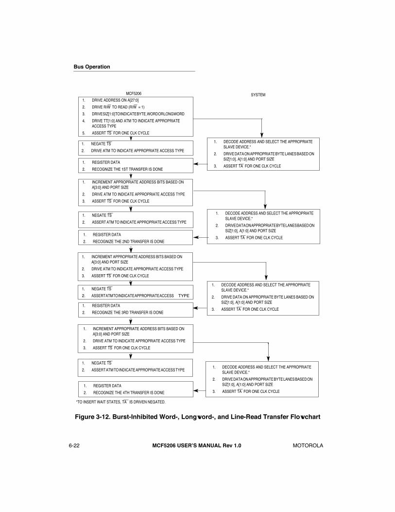
Bus Operation
6-22 MCF5206 USERÕS MANUAL Rev 1.0 MOTOROLA
Figure 3-12. Burst-Inhibited Word-, Longword-, and Line-Read Transfer Flowchart
1. INCREMENT APPROPRIATE ADDRESS BITS BASED ON A[3:0] AND PORT SIZE
2. DRIVE ATM TO INDICATE APPROPRIATE ACCESS TYPE
3. ASSERT TS FOR ONE CLK CYCLE
1. NEGATE TS
2. DRIVE ATM TO INDICATE APPROPRIATE ACCESS TYPE
1. INCREMENT APPROPRIATE ADDRESS BITS BASED ON A[3:0] AND PORT SIZE
2. DRIVE ATM TO INDICATE APPROPRIATE ACCESS TYPE
3. ASSERT TS FOR ONE CLK CYCLE
MCF5206 SYSTEM1. DRIVE ADDRESS ON A[27:0]
2. DRIVE R/W TO READ (R/W = 1)
3. DRIVE SIZ[1:0] TO INDICATE BYTE, WORD OR LONGWORD
4. DRIVE TT[1:0] AND ATM TO INDICATE APPROPRIATE ACCESS TYPE
5. ASSERT TS FOR ONE CLK CYCLE
1. REGISTER DATA
2. RECOGNIZE THE 2ND TRANSFER IS DONE
1. NEGATE TS
2. ASSERT ATM TO INDICATE APPROPRIATE ACCESS TYPE
1. REGISTER DATA
2. RECOGNIZE THE 3RD TRANSFER IS DONE
1. NEGATE TS
2. ASSERT ATM TO INDICATE APPROPRIATE ACCESS TYPE
1. NEGATE TS
2. ASSERT ATM TO INDICATE APPROPRIATE ACCESS TYPE
1. REGISTER DATA
2. RECOGNIZE THE 4TH TRANSFER IS DONE
1. INCREMENT APPROPRIATE ADDRESS BITS BASED ON A[3:0] AND PORT SIZE
2. DRIVE ATM TO INDICATE APPROPRIATE ACCESS TYPE
3. ASSERT TS FOR ONE CLK CYCLE
1. DECODE ADDRESS AND SELECT THE APPROPRIATE SLAVE DEVICE.*
2. DRIVE DATA ON APPROPRIATE BYTE LANES BASED ON SIZ[1:0], A[1:0] AND PORT SIZE
3. ASSERT TA FOR ONE CLK CYCLE
1. DECODE ADDRESS AND SELECT THE APPROPRIATE SLAVE DEVICE.*
2. DRIVE DATA ON APPROPRIATE BYTE LANES BASED ON SIZ[1:0], A[1:0] AND PORT SIZE
3. ASSERT TA FOR ONE CLK CYCLE
1. DECODE ADDRESS AND SELECT THE APPROPRIATE SLAVE DEVICE.*
2. DRIVE DATA ON APPROPRIATE BYTE LANES BASED ON SIZ[1:0], A[1:0] AND PORT SIZE
3. ASSERT TA FOR ONE CLK CYCLE
1. DECODE ADDRESS AND SELECT THE APPROPRIATE SLAVE DEVICE.*
2. DRIVE DATA ON APPROPRIATE BYTE LANES BASED ON SIZ[1:0], A[1:0] AND PORT SIZE
3. ASSERT TA FOR ONE CLK CYCLE
*TO INSERT WAIT STATES, TA IS DRIVEN NEGATED.
1. REGISTER DATA
2. RECOGNIZE THE 1ST TRANSFER IS DONE

Bus Operation
MOTOROLA MCF5206 USERÕS MANUAL Rev 1.0 6-23
Figure 6-13 shows a burst-inhibited supervisor code longword-read transfer from an 8-bit port.
Figure 3-13. Burst-Inhibited Longword Read From an 8-Bit Port (No Wait States)
Clock 1 (C1)
The read cycle starts in C1. During C1, the MCF5206 places valid values on the address bus (A[27:0]) and transfer control signals. The transfer type (TT[1:0]) signals identify the specific access type and drives ATM high to identify the transfer as code. The read/write (R/W) signal is driven high for a read cycle, and the size signals (SIZ[1:0]) are driven to $1 to indicate a byte transfer. The MCF5206 asserts TS to indicate the beginning of a bus cycle.
Clock 2 (C2)
During C2, the MCF5206 negates TS and drives ATM high to identify the transfer as supervisor. The selected device(s) places the first byte of the addressed data onto D[31:24] and asserts TA. At the end of C2, the MCF5206 samples the level of TA and if TA is asserted, latches the current value of D[31:24]. If TA is asserted, the transfer of the first byte of the longword read is complete. If TA is negated, the MCF5206 continues to
TS
A[27:2]
R/W
CLK
TT[1:0]
ATM
TA
D[31:24]
TEA
SIZ[1:0]
C1 C2
$1
$0
C3
$ADDR
C4
A[1:0] $0 $1 $2 $3
C5 C6 C7 C8
ATA

Bus Operation
6-24 MCF5206 USERÕS MANUAL Rev 1.0 MOTOROLA
sample TA and inserts wait states instead of terminating the transfer. The MCF5206 continues to sample TA on successive rising edges of CLK until it is asserted.
Clock 3 (C3)
The MCF5206 increments A[1:0] to address the second byte of the longword transfer. The MCF5206 continues to drive transfer type (TT[1:0]), read/write (R/W) and size (SIZ[1:0]) signals to indicate a byte read. Access transfer mode (ATM) is driven high to indicate the transfer as code. The MCF5206 asserts TS to indicate the beginning of the second transfer of the bus cycle.
Clock 4 (C4)
This clock is identical to C2, except that once TA is recognized asserted, the latched value corresponds to the second byte of data for the longword transfer.
Clock 5 (C5)
This clock is identical to C3, except the address is incremented to address the third byte of the longword transfer.
Clock 6 (C6)
This clock is identical to C2, except that once TA is recognized asserted, the latched value corresponds to the third byte of data for the longword transfer.
Clock 7 (C7)
This clock is identical to C3, except the address is incremented to address the fourth byte of the longword transfer.
Clock 8 (C8)
This clock is identical to C2, except that once TA is recognized asserted, the latched value corresponds to the fourth byte of data for the longword. This is the last CLK cycle of the longword-read transfer. The selected device negates TA signal and three-states D[31:24] after the next rising edge of CLK.
6.5.5 Burst-Inhibited Write Transfer: Word, Longword, and LineThe basic transfer of a burst-inhibited write is the same as ÒnormalÓ write with the addition of more transfers until the entire operand has been accessed. Burst-inhibited write transfers can be from 2 to 16 transfers long. Figure 6-14 is a flowchart for burst-inhibited write transfers (4 transfers long) to 8-, 16-, or 32-bit ports. Bus operations are similar for each case and vary only with the size indicated, the portion of the data bus used for the transfer, and the specific number of cycles needed for each transfer.

Bus Operation
MOTOROLA MCF5206 USERÕS MANUAL Rev 1.0 6-25
MCF5206 SYSTEM
1. DRIVE ADDRESS ON A[27:0]
2. DRIVE R/W TO WRITE (R/W = 0)
3. DRIVE SIZ[1:0] TO INDICATE BYTE, WORD OR LONGWORD
4. DRIVE TT[1:0] AND ATM TO INDICATE APPROPRIATE ACCESS TYPE
5. ASSERT TS FOR ONE CLK CYCLE
1. NEGATE TS
2. DRIVE ATM TO INDICATE APPROPRIATE ACCESS TYPE
3. DRIVE DATA ON APPROPRIATE BYTE LANES BASED ON SIZ[1:0], A[1:0] AND PORT SIZE
1. RECOGNIZE THE 1ST TRANSFER IS DONE
2. INCREMENT APPROPRIATE ADDRESS BITS BASED ON SIZ[1:0], A[3:0] AND PORT SIZE
3. DRIVE ATM TO INDICATE APPROPRIATE ACCESS TYPE
4. ASSERT TS FOR ONE CLK CYCLE
1. RECOGNIZE THE 4TH TRANSFER IS DONE
2. THREE-STATE D[31:0]
1. DECODE ADDRESS AND SELECT THE APPROPRIATE SLAVE DEVICE.*
2. CAPTURE DATA FROM THE APPROPRIATE BYTE LANES BASED ON SIZ[1:0], A[1:0] AND PORT SIZE
3. ASSERT TA FOR ONE CLK CYCLE
*TO INSERT WAIT STATES, TA IS DRIVEN NEGATED .
1. DECODE ADDRESS AND SELECT THE APPROPRIATE SLAVE DEVICE.*
2. CAPTURE DATA FROM THE APPROPRIATE BYTE LANES BASED ON SIZ[1:0], A[1:0] AND PORT SIZE
3. ASSERT TA FOR ONE CLK CYCLE
1. NEGATE TS
2. DRIVE ATM TO INDICATE APPROPRIATE ACCESS TYPE
3. DRIVE DATA ON APPROPRIATE BYTE LANES BASED ON SIZ[1:0], A[1:0] AND PORT SIZE
1. RECOGNIZE THE 3RD TRANSFER IS DONE
2. INCREMENT APPROPRIATE ADDRESS BITS BASED ON SIZ[1:0], A[3:0] AND PORT SIZE
3. DRIVE ATM TO INDICATE APPROPRIATE ACCESS TYPE
4. ASSERT TS FOR ONE CLK CYCLE
1. NEGATE TS
2. DRIVE ATM TO INDICATE APPROPRIATE ACCESS TYPE
3. DRIVE DATA ON APPROPRIATE BYTE LANES BASED ON SIZ[1:0], A[1:0] AND PORT SIZE
1. DECODE ADDRESS AND SELECT THE APPROPRIATE SLAVE DEVICE.*
2. CAPTURE DATA FROM THE APPROPRIATE BYTE LANES BASED ON SIZ[1:0], A[1:0] AND PORT SIZE
3. ASSERT TA FOR ONE CLK CYCLE
1. RECOGNIZE THE 2ND TRANSFER IS DONE
2. INCREMENT APPROPRIATE ADDRESS BITS BASED ON SIZ[1:0], A[3:0] AND PORT SIZE
3. DRIVE ATM TO INDICATE APPROPRIATE ACCESS TYPE
4. ASSERT TS FOR ONE CLK CYCLE
1. DECODE ADDRESS AND SELECT THE APPROPRIATE SLAVE DEVICE.*
2. CAPTURE DATA FROM THE APPROPRIATE BYTE LANES BASED ON SIZ[1:0], A[1:0] AND PORT SIZE
3. ASSERT TA FOR ONE CLK CYCLE
1. NEGATE TS
2. DRIVE ATM TO INDICATE APPROPRIATE ACCESS TYPE
3. DRIVE DATA ON APPROPRIATE BYTE LANES BASED ON SIZ[1:0], A[1:0] AND PORT SIZE

Bus Operation
6-26 MCF5206 USERÕS MANUAL Rev 1.0 MOTOROLA
Figure 6-14. Burst-Inhibited Byte-, Word-, and Longword-Write Transfer Flowchart
Figure 6-15 shows a burst-inhibited supervisor data longword-write transfer to a 16-bit port.
Figure 6-15. Burst-Inhibited Longword-Write Transfer to a 16-Bit Port (No Wait States)
Clock 1 (C1)
The write cycle starts in C1. During C1, the MCF5206 places valid values on the address bus (A[27:0]) and transfer control signals. The transfer type (TT[1:0]) signals identify the specific access type and ATM identifies the transfer as data. The read/write (R/W) signal is driven low for a write cycle, and the size signals (SIZ[1:0]) are driven to $2 to indicate a word transfer. The MCF5206 asserts TS to indicate the beginning of a bus cycle.
Clock 2 (C2)
During C2, the MCF5206 negates TS, drives ATM high to identify the transfer as supervisor and places the data on the data bus (D[31:0]). The selected device(s) asserts TA if it is ready to latch the data. At the end of C2, the selected device latches the current
TS
A[27:2]
R/W
CLK
TT[1:0]
ATM
TA
D[31:0]
TEA
SIZ[1:0]
C1 C2
$0
C3 C4
$ADDR
A[1:0] $0 $2
ATA
$2

Bus Operation
MOTOROLA MCF5206 USERÕS MANUAL Rev 1.0 6-27
value of D[31:16], and the MCF5206 samples the level of TA. If TA is asserted, the transfer of the first word is complete. If TA is negated, the MCF5206 continues to output the data and inserts wait states instead of terminating the transfer. The MCF5206 continues to sample TA on successive rising edges of CLK until it is asserted.
Clock 3 (C3)
The MCF5206 increments A[1:0] to address the next word, asserts TS and drives ATM low to identify the transfer as code or data.
Clock 4 (C4)
This clock is identical to C2, except that the data driven corresponds to the second word of data. This is the last CLK cycle of the longword-write transfer and the MCF5206 three-states D[31:0] at the start of the next CLK cycle.
6.5.6 Asynchronous-Acknowledge Read TransferThe MCF5206 provides an asynchronous acknowledge that can be used for termination of all MCF5206 transfers except accesses to DRAM. ATA is synchronized internally before being used and must meet the specified setup and hold times to CLK only if recognition by a specific CLK rising edge is required. Because of the internal synchronization of ATA, data must be driven on the bus until the asynchronous transfer acknowledge is recognized internally. If transfer error acknowledge (TEA) is asserted while ATA is being synchronized internally, the transfer is terminated in an error.
NOTE
The internal synchronized version of (ATA) is referred to asÔÔinternal asynchronous transfer acknowledge.ÕÕ Because ofthe time required to internally synchronize ATA during a readcycle, data is latched on the rising edge of CLK when theinternal asynchronous transfer acknowledge is asserted.Consequently, data must remain valid for at least one CLKcycle after the assertion of ATA. Similarly, during a write cycle,data is driven until the rising edge of CLK when the internalasynchronous transfer acknowledge is asserted.
Figure 6-16 is a flowchart for read transfers to 8-, 16-, or 32-bit ports with asynchronous termination. Bus operations are similar for each case and vary only with the size indicated,
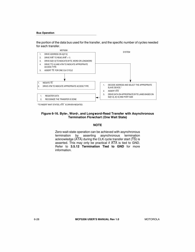
Bus Operation
6-28 MCF5206 USERÕS MANUAL Rev 1.0 MOTOROLA
the portion of the data bus used for the transfer, and the specific number of cycles needed for each transfer.
Figure 6-16. Byte-, Word-, and Longword-Read Transfer with Asynchronous Termination Flowchart (One Wait State)
NOTE
Zero-wait-state operation can be achieved with asynchronoustermination by asserting asynchronous terminationacknowledge (ATA) during the CLK cycle transfer start (TS) isasserted. This may only be practical if ATA is tied to GND.Refer to 3.5.12 Termination Tied to GND for moreinformation.
MCF5206SYSTEM
1. DRIVE ADDRESS ON A[27:0]
2. DRIVE R/W TO READ (R/W = 1)
3. DRIVE SIZ[1:0] TO INDICATE BYTE, WORD OR LONGWORD
4. DRIVE TT[1:0] AND ATM TO INDICATE APPROPRIATE ACCESS TYPE
5. ASSERT TS FOR ONE CLK CYCLE
1. NEGATE TS
2. DRIVE ATM TO INDICATE APPROPRIATE ACCESS TYPE
*TO INSERT WAIT STATES, ATA IS DRIVEN NEGATED.
1. DECODE ADDRESS AND SELECT THE APPROPRIATE SLAVE DEVICE.*
2. ASSERT ATA
3. DRIVE DATA ON APPROPRIATE BYTE LANES BASED ON SIZ[1:0], A[1:0] AND PORT SIZE1. REGISTER DATA
2. RECOGNIZE THE TRANSFER IS DONE
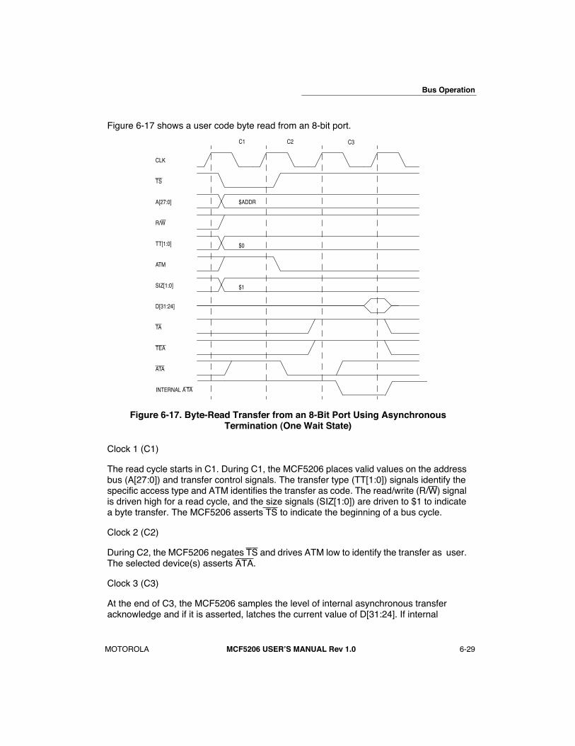
Bus Operation
MOTOROLA MCF5206 USERÕS MANUAL Rev 1.0 6-29
Figure 6-17 shows a user code byte read from an 8-bit port.
Figure 6-17. Byte-Read Transfer from an 8-Bit Port Using Asynchronous Termination (One Wait State)
Clock 1 (C1)
The read cycle starts in C1. During C1, the MCF5206 places valid values on the address bus (A[27:0]) and transfer control signals. The transfer type (TT[1:0]) signals identify the specific access type and ATM identifies the transfer as code. The read/write (R/W) signal is driven high for a read cycle, and the size signals (SIZ[1:0]) are driven to $1 to indicate a byte transfer. The MCF5206 asserts TS to indicate the beginning of a bus cycle.
Clock 2 (C2)
During C2, the MCF5206 negates TS and drives ATM low to identify the transfer as user. The selected device(s) asserts ATA.
Clock 3 (C3)
At the end of C3, the MCF5206 samples the level of internal asynchronous transfer acknowledge and if it is asserted, latches the current value of D[31:24]. If internal
TS
A[27:0]
R/W
CLK
TT[1:0]
ATM
ATA
D[31:24]
TEA
SIZ[1:0]
C1 C2
$1
$0
$ADDR
C3
TA
INTERNAL A TA
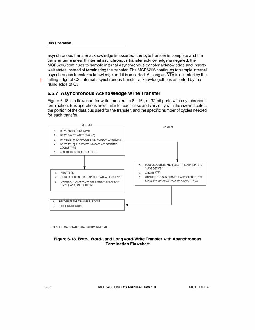
Bus Operation
6-30 MCF5206 USERÕS MANUAL Rev 1.0 MOTOROLA
asynchronous transfer acknowledge is asserted, the byte transfer is complete and the transfer terminates. If internal asynchronous transfer acknowledge is negated, the MCF5206 continues to sample internal asynchronous transfer acknowledge and inserts wait states instead of terminating the transfer. The MCF5206 continues to sample internal asynchronous transfer acknowledge until it is asserted. As long as ATA is asserted by the falling edge of C2, internal asynchronous transfer acknowledgethe is asserted by the rising edge of C3.
6.5.7 Asynchronous Acknowledge Write TransferFigure 6-18 is a flowchart for write transfers to 8-, 16-, or 32-bit ports with asynchronous termination. Bus operations are similar for each case and vary only with the size indicated, the portion of the data bus used for the transfer, and the specific number of cycles needed for each transfer.
Figure 6-18. Byte-, Word-, and Longword-Write Transfer with Asynchronous Termination Flowchart
MCF5206SYSTEM
1. DRIVE ADDRESS ON A[27:0]
2. DRIVE R/W TO WRITE (R/W = 0)
3. DRIVE SIZ[1:0] TO INDICATE BYTE, WORD OR LONGWORD
4. DRIVE TT[1:0] AND ATM TO INDICATE APPROPRIATE ACCESS TYPE
5. ASSERT TS FOR ONE CLK CYCLE
1. RECOGNIZE THE TRANSFER IS DONE
2. THREE-STATE D[31:0]
*TO INSERT WAIT STATES, ATA IS DRIVEN NEGATED.
1. DECODE ADDRESS AND SELECT THE APPROPRIATE SLAVE DEVICE.*
2. ASSERT ATA
3. CAPTURE THE DATA FROM THE APPROPRIATE BYTE LANES BASED ON SIZ[1:0], A[1:0] AND PORT SIZE
1. NEGATE TS
2. DRIVE ATM TO INDICATE APPROPRIATE ACCESS TYPE
3. DRIVE DATA ON APPROPRIATE BYTE LANES BASED ON SIZ[1:0], A[1:0] AND PORT SIZE

Bus Operation
MOTOROLA MCF5206 USERÕS MANUAL Rev 1.0 6-31
Figure 6-19 shows a user data byte transfer to a 32-bit port with asynchronous termination.
Figure 6-19. Byte-Write Transfer to a 32-Bit Port Using Asynchronous Termination (One Wait State)
Clock 1 (C1)
The write cycle starts in C1. During C1, the MCF5206 places valid values on the address bus (A[27:0]) and transfer control signals. The transfer type (TT[1:0]) signals identify the specific access type and ATM identifies the transfer as data. The read/write (R/W) signal is driven low for a write cycle, and the size signals (SIZ[1:0]) are driven to $1 to indicate a byte transfer. The MCF5206 asserts TS to indicate the beginning of a bus cycle.
Clock 2 (C2)
During C2, the MCF5206 negates TS, drives ATM low to identify the transfer as user and places the data on the data bus (D[31:0]). The selected slave device asserts ATA. The selected slave device may latch the data present on the data bus or may wait until the end of Clock 3 (after internal asynchronous transfer acknowledge has been asserted).
TS
A[27:0]
R/W
CLK
TT[1:0]
ATM
TA
D[31:0]
TEA
SIZ[1:0]
C1 C2
$0
C3
$ADDR
ATA
$1
INTERNAL ATA

Bus Operation
6-32 MCF5206 USERÕS MANUAL Rev 1.0 MOTOROLA
Clock 3 (C3)
At the end of C3, the MCF5206 samples the level of internal asynchronous transfer acknowledge and if it is asserted, the transfer of the byte is complete and the transfer terminates. If internal asynchronous transfer acknowledge is negated, the MCF5206 continues to sample internal asynchronous transfer acknowledge and inserts wait states instead of terminating the transfer. The MCF5206 continues to sample internal asynchronous transfer acknowledge until it is asserted. As long as ATA is asserted by the falling edge of C2, internal asynchronous transfer acknowledge is asserted by the rising edge of C3.
6.5.8 Bursting Read Transfers: Word, Longword, and Line with Asynchronous AcknowledgeIf the burst-enable bit in the appropriate Chip Select Control Register (CSCR) or Default Memory Control Register (DMCR) is set to 1 and the operand size is larger than the port size of the memory being accessed, the MCF5206 performs word, longword, and line transfers in burst mode. When burst mode is selected and the transfer is not to DRAM, the transfer can be terminated synchronously using TA, or asynchronously using ATA. The transfer attributes are the same for both the synchronous and asynchronously terminated burst transfers.
Figure 6-20 is a flowchart for bursting read transfers to 8-, 16-, or 32-bit ports using asynchronous termination. Bus operations are similar for each case and vary only with the size indicated, the portion of the data bus needed for the transfer, and the specific number

Bus Operation
MOTOROLA MCF5206 USERÕS MANUAL Rev 1.0 6-33
of cycles used for each transfer. A bursted transfer can be from two to 16 transfers long. The flow chart shown is for four bursting transfers.
Figure 6-20. Bursting Word-, Longword-, and Line-Read Transfer with Asynchronous Termination Flowchart
MCF5206 SYSTEM
1. DRIVE ADDRESS ON A[27:0]
2. DRIVE R/W TO READ (R/W = 1)
3. DRIVE SIZ[1:0] TO INDICATE WORD, LONGWORD OR LINE
4. DRIVE TT[1:0] AND ATM TO INDICATE APPROPRIATE ACCESS TYPE
5. ASSERT TS FOR ONE CLK CYCLE
1. NEGATE TS
2. DRIVE ATM TO INDICATE APPROPRIATE ACCESS TYPE
1. REGISTER DATA
2. INCREMENT APPROPRIATE ADDRESS BITS BASED ON SIZ[1:0], A[3:0] AND PORT SIZE
1. DECODE ADDRESS AND SELECT THE APPROPRIATE SLAVE DEVICE.*
2. ASSERT ATA
3. DRIVE DATA ON APPROPRIATE BYTE LANES BASED ON SIZ[1:0], A[1:0] AND PORT SIZE
*TO INSERT WAIT STATES, ATA IS DRIVEN NEGATED.
1. DECODE ADDRESS AND SELECT THE APPROPRIATE SLAVE DEVICE.*
2. ASSERT ATA
3. DRIVE DATA ON APPROPRIATE BYTE LANES BASED ON SIZ[1:0], A[1:0] AND PORT SIZE
1. DECODE ADDRESS AND SELECT THE APPROPRIATE SLAVE DEVICE.*
2. ASSERT ATA
3. DRIVE DATA ON APPROPRIATE BYTE LANES BASED ON SIZ[1:0], A[1:0] AND PORT SIZE
1. DECODE ADDRESS AND SELECT THE APPROPRIATE SLAVE DEVICE.*
2. ASSERT ATA
3. DRIVE DATA ON APPROPRIATE BYTE LANES BASED ON SIZ[1:0], A[1:0] AND PORT SIZE
1. REGISTER DATA
2. RECOGNIZE THE TRANSFER IS DONE
1. REGISTER DATA
2. INCREMENT APPROPRIATE ADDRESS BITS BASED ON SIZ[1:0], A[3:0] AND PORT SIZE
1. REGISTER DATA
2. INCREMENT APPROPRIATE ADDRESS BITS BASED ON SIZ[1:0], A[3:0] AND PORT SIZE
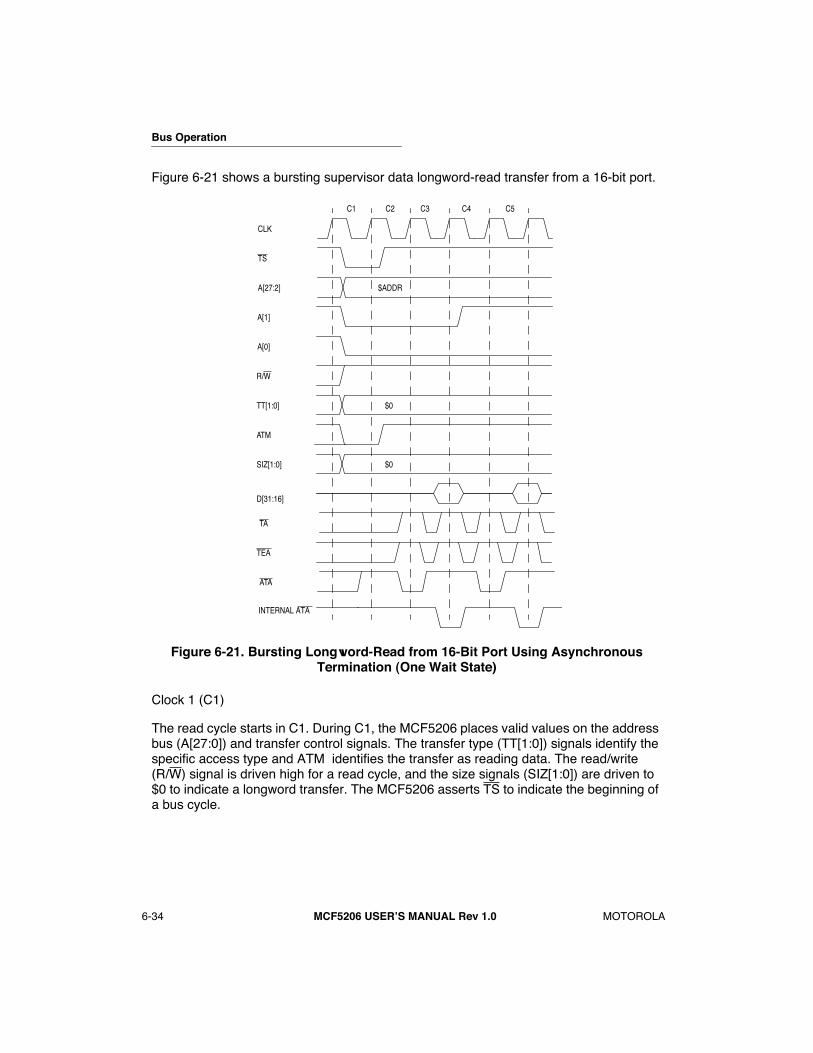
Bus Operation
6-34 MCF5206 USERÕS MANUAL Rev 1.0 MOTOROLA
Figure 6-21 shows a bursting supervisor data longword-read transfer from a 16-bit port.
Figure 6-21. Bursting Longword-Read from 16-Bit Port Using Asynchronous Termination (One Wait State)
Clock 1 (C1)
The read cycle starts in C1. During C1, the MCF5206 places valid values on the address bus (A[27:0]) and transfer control signals. The transfer type (TT[1:0]) signals identify the specific access type and ATM identifies the transfer as reading data. The read/write (R/W) signal is driven high for a read cycle, and the size signals (SIZ[1:0]) are driven to $0 to indicate a longword transfer. The MCF5206 asserts TS to indicate the beginning of a bus cycle.
TS
A[27:2]
R/W
CLK
TT[1:0]
ATM
ATA
D[31:16]
TEA
SIZ[1:0]
C1 C2
$0
$0
C3
$ADDR
C4 C5
A[1]
A[0]
TA
INTERNAL ATA
Bus Operation
MOTOROLA MCF5206 USERÕS MANUAL Rev 1.0 6-35
Clock 2 (C2)
During C2, the MCF5206 negates TS, drives ATM high to identify the transfer as supervisor. The selected device(s) asserts ATA.
Clock 3 (C3)
At the end of C3, the MCF5206 samples the level of internal asynchronous transfer acknowledge and if it is asserted, latches the current value of D[31:16]. If internal asynchronous transfer acknowledge is asserted, the transfer of the first word is complete. If internal asynchronous transfer acknowledge is negated, the MCF5206 continues to sample internal asynchronous transfer acknowledge and inserts wait states instead of terminating the transfer. The MCF5206 continues to sample internal asynchronous transfer acknowledge until it is asserted. As long as ATA is asserted by the falling edge of C2, internal asynchronous transfer acknowledge is asserted by the rising edge of C3.
Clock 4 (C4)
The MCF5206 increments A[1:0] to address the next word. The selected device(s) asserts ATA.
Clock 5 (C5)
At the end of C5, the MCF5206 samples the level of internal asynchronous transfer acknowledge and if it is asserted, latches the current value of D[31:16]. If internal asynchronous transfer acknowledge is asserted, the transfer of the second word is complete and the transfer is terminated. If internal asynchronous transfer acknowledge is negated, the MCF5206 continues to sample internal asynchronous transfer acknowledge and inserts wait states instead of terminating the transfer. The MCF5206 continues to sample internal asynchronous transfer acknowledge until it is asserted. As long as ATA is asserted by the falling edge of C4, internal asynchronous transfer acknowledge is asserted by the rising edge of C5.
6.5.9 Bursting Write Transfers: Word, Longword, and Line with Asynchronous AcknowledgeFigure 6-22 is a flowchart for bursting write transfers (four transfers long) to 8-, 16-, or 32-bit ports using asynchronous termination. Bus operations are similar for each case and vary only with the size indicated, the portion of the data bus used for the transfer, and the specific number of cycles needed for each transfer. A bursted transfer can be from two to 16 transfers long.
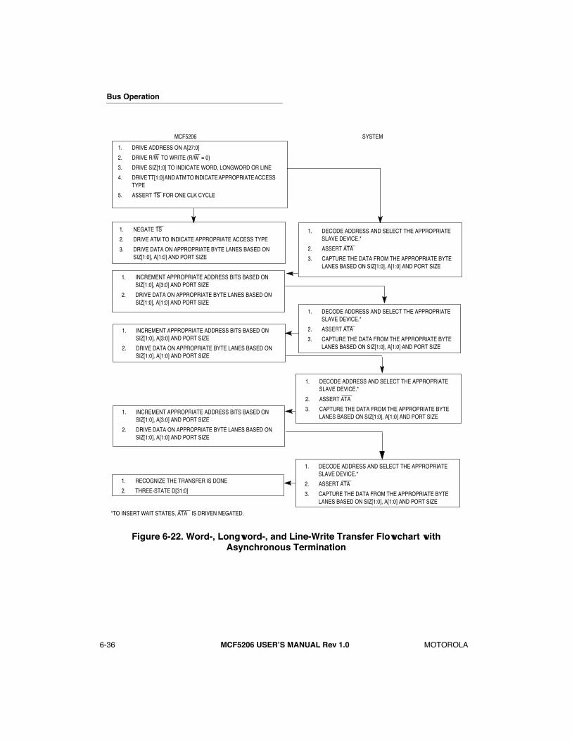
Bus Operation
6-36 MCF5206 USERÕS MANUAL Rev 1.0 MOTOROLA
Figure 6-22. Word-, Longword-, and Line-Write Transfer Flowchart with Asynchronous Termination
MCF5206 SYSTEM
1. DRIVE ADDRESS ON A[27:0]
2. DRIVE R/W TO WRITE (R/W = 0)
3. DRIVE SIZ[1:0] TO INDICATE WORD, LONGWORD OR LINE
4. DRIVE TT[1:0] AND ATM TO INDICATE APPROPRIATE ACCESS TYPE
5. ASSERT TS FOR ONE CLK CYCLE
1. NEGATE TS
2. DRIVE ATM TO INDICATE APPROPRIATE ACCESS TYPE
3. DRIVE DATA ON APPROPRIATE BYTE LANES BASED ON SIZ[1:0], A[1:0] AND PORT SIZE
*TO INSERT WAIT STATES, ATA IS DRIVEN NEGATED.
1. DECODE ADDRESS AND SELECT THE APPROPRIATE SLAVE DEVICE.*
2. ASSERT ATA
3. CAPTURE THE DATA FROM THE APPROPRIATE BYTE LANES BASED ON SIZ[1:0], A[1:0] AND PORT SIZE
1. DECODE ADDRESS AND SELECT THE APPROPRIATE SLAVE DEVICE.*
2. ASSERT ATA
3. CAPTURE THE DATA FROM THE APPROPRIATE BYTE LANES BASED ON SIZ[1:0], A[1:0] AND PORT SIZE
1. DECODE ADDRESS AND SELECT THE APPROPRIATE SLAVE DEVICE.*
2. ASSERT ATA
3. CAPTURE THE DATA FROM THE APPROPRIATE BYTE LANES BASED ON SIZ[1:0], A[1:0] AND PORT SIZE
1. DECODE ADDRESS AND SELECT THE APPROPRIATE SLAVE DEVICE.*
2. ASSERT ATA
3. CAPTURE THE DATA FROM THE APPROPRIATE BYTE LANES BASED ON SIZ[1:0], A[1:0] AND PORT SIZE
1. INCREMENT APPROPRIATE ADDRESS BITS BASED ON SIZ[1:0], A[3:0] AND PORT SIZE
2. DRIVE DATA ON APPROPRIATE BYTE LANES BASED ON SIZ[1:0], A[1:0] AND PORT SIZE
1. INCREMENT APPROPRIATE ADDRESS BITS BASED ON SIZ[1:0], A[3:0] AND PORT SIZE
2. DRIVE DATA ON APPROPRIATE BYTE LANES BASED ON SIZ[1:0], A[1:0] AND PORT SIZE
1. RECOGNIZE THE TRANSFER IS DONE
2. THREE-STATE D[31:0]
1. INCREMENT APPROPRIATE ADDRESS BITS BASED ON SIZ[1:0], A[3:0] AND PORT SIZE
2. DRIVE DATA ON APPROPRIATE BYTE LANES BASED ON SIZ[1:0], A[1:0] AND PORT SIZE
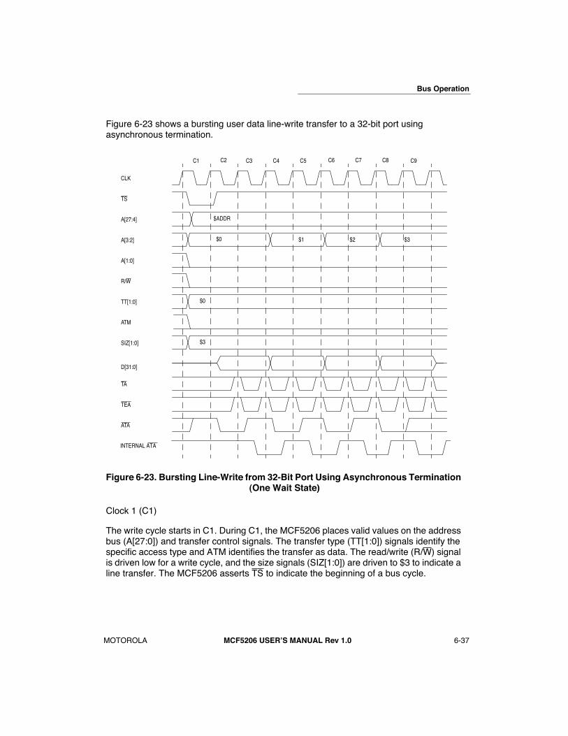
Bus Operation
MOTOROLA MCF5206 USERÕS MANUAL Rev 1.0 6-37
Figure 6-23 shows a bursting user data line-write transfer to a 32-bit port using asynchronous termination.
Figure 6-23. Bursting Line-Write from 32-Bit Port Using Asynchronous Termination (One Wait State)
Clock 1 (C1)
The write cycle starts in C1. During C1, the MCF5206 places valid values on the address bus (A[27:0]) and transfer control signals. The transfer type (TT[1:0]) signals identify the specific access type and ATM identifies the transfer as data. The read/write (R/W) signal is driven low for a write cycle, and the size signals (SIZ[1:0]) are driven to $3 to indicate a line transfer. The MCF5206 asserts TS to indicate the beginning of a bus cycle.
TS
A[27:4]
R/W
CLK
TT[1:0]
ATM
ATA
D[31:0]
TEA
SIZ[1:0]
C1 C2
$3
$0
C3 C4 C5 C6 C7 C8 C9
$ADDR
A[3:2] $0
A[1:0]
$1 $2 $3
TA
INTERNAL ATA

Bus Operation
6-38 MCF5206 USERÕS MANUAL Rev 1.0 MOTOROLA
Clock 2 (C2)
During C2, the MCF5206 negates TS, drives ATM low to identify the transfer as user and places the data on the data bus (D[31:0]). The selected device(s) asserts ATA if it is ready to latch the data.
Clock 3 (C3)
If the selected device asserted asynchronous transfer acknowledge during C2, the selected device must latch the data by the end of C3. At the end of C3, the MCF5206 samples the level of internal asynchronous transfer acknowledge. If internal asynchronous transfer acknowledge is asserted, the transfer of the first longword is complete. If internal asynchronous transfer acknowledge is negated, the MCF5206 continues to sample internal asynchronous transfer acknowledge and inserts wait states instead of terminating the transfer. The MCF5206 continues to sample internal asynchronous transfer acknowledge until it is asserted. As long as ATA is asserted by the falling edge of C2, the internal asynchronous transfer acknowledge is asserted by the rising edge of C3.
Clock 4 (C4)
The MCF5206 increments A[3:2] to address the next longword of the line transfer and drives D[31:0] with the second longword of data. The selected device(s) asserts ATA if it is ready to latch the data. At the end of C4, the MCF5206 samples the level of internal ATA and if it is asserted, the second longword transfer of the line write is complete. If internal ATA is negated, the MCF5206 continues to sample internal ATA and inserts wait states instead of terminating the transfer. The MCF5206 continues to sample internal ATA on successive rising edge of CLK until it is asserted.
Clock 5 (C5)
This clock is identical to C3, except that the data value corresponds to the second longword of data for the burst.
Clock 6 (C6)
This clock is identical to C4, except that once internal ATA is asserted, the address and the data values correspond to the third longword of data for the burst.
Clock 7 (C7)
This clock is identical to C3, except that the data value corresponds to the third longword of data for the burst.
Clock 8 (C8)
This clock is identical to C4, except that once internal ATA is asserted the address and data value correspond to the fourth longword of data for the burst.

Bus Operation
MOTOROLA MCF5206 USERÕS MANUAL Rev 1.0 6-39
Clock 9 (C9)
This clock is identical to C3, except that the data value corresponds to the fourth longword of data for the line. This is the last CLK cycle of the line write transfer and the MCF5206 three-states D[31:0] at the start of the next CLK cycle.
6.5.10 Burst-Inhibited Read Transfers: Word, Longword, and Line with Asynchronous AcknowledgeIf the burst-enable bit is cleared in the appropriate Chip Select Control Register (CSCR) or Default Memory Control Register (DMCR) and the operand size is larger than the port size of the memory being accessed, the MCF5206 performs word, longword, and line transfers in burst-inhibited mode. When burst-inhibit mode is selected, the size of the transfer (indicated by SIZ[1:0]) reflects the port size if the operand being read is larger than the port size, or the operand size if the port size is larger than the operand size. A transfer size of line (SIZ[1:0] = $3) is never indicated in burst-inhibited mode. If the operand size is line, the size pins (SIZ[1:0]) always indicates the port size.
The basic transfer of a burst-inhibited read using asynchronous termination is the same as ÒnormalÓ read using asynchronous termination with the addition of more transfers, until the entire operand has been accessed. Figure 6-24 is a flowchart for burst-inhibited read transfers to 8-, 16-, or 32-bit ports with asynchronous termination. Bus operations are similar for each case and vary only with the size indicated, the portion of the data bus used for the transfer, and the specific number of cycles needed for each transfer. The flowchart is specifically for a burst-inhibited transfer of four transfers long.
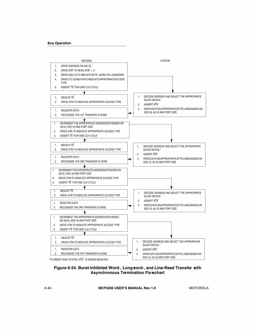
Bus Operation
6-40 MCF5206 USERÕS MANUAL Rev 1.0 MOTOROLA
Figure 6-24. Burst-Inhibited Word-, Longword-, and Line-Read Transfer with Asynchronous Termination Flowchart
1. REGISTER DATA
2. RECOGNIZE THE 1ST TRANSFER IS DONE
1. NEGATE TS
2. DRIVE ATM TO INDICATE APPROPRIATE ACCESS TYPE
1. INCREMENT THE APPROPRIATE ADDRESS BITS BASED ON A[3:0], SIZ[1:0] AND PORT SIZE
2. DRIVE ATM TO INDICATE APPROPRIATE ACCESS TYPE
3. ASSERT TS FOR ONE CLK CYCLE
MCF5206 SYSTEM
1. DRIVE ADDRESS ON A[27:0]
2. DRIVE R/W TO READ (R/W = 1)
3. DRIVE SIZ[1:0] TO INDICATE BYTE, WORD OR LONGWORD
4. DRIVE TT[1:0] AND ATM TO INDICATE APPROPRIATE ACCESS TYPE
5. ASSERT TS FOR ONE CLK CYCLE
1. REGISTER DATA
2. RECOGNIZE THE 2ND TRANSFER IS DONE
1. INCREMENT THE APPROPRIATE ADDRESS BITS BASED ON A[3:0], SIZ[1:0] AND PORT SIZE
2. DRIVE ATM TO INDICATE APPROPRIATE ACCESS TYPE
3. ASSERT TS FOR ONE CLK CYCLE
1. REGISTER DATA
2. RECOGNIZE THE 3RD TRANSFER IS DONE
1. NEGATE TS
2. DRIVE ATM TO INDICATE APPROPRIATE ACCESS TYPE
1. INCREMENT THE APPROPRIATE ADDRESS BITS BASED ON A[3:0], SIZ[1:0] AND PORT SIZE
2. DRIVE ATM TO INDICATE APPROPRIATE ACCESS TYPE
3. ASSERT TS FOR ONE CLK CYCLE
1. REGISTER DATA
2. RECOGNIZE THE 4TH TRANSFER IS DONE
1. NEGATE TS
2. DRIVE ATM TO INDICATE APPROPRIATE ACCESS TYPE
1. DECODE ADDRESS AND SELECT THE APPROPRIATE SLAVE DEVICE.*
2. ASSERT ATA
3. DRIVE DATA ON APPROPRIATE BYTE LANES BASED ON SIZ[1:0], A[1:0] AND PORT SIZE
*TO INSERT WAIT STATES, ATA IS DRIVEN NEGATED.
1. DECODE ADDRESS AND SELECT THE APPROPRIATE SLAVE DEVICE.*
2. ASSERT ATA
3. DRIVE DATA ON APPROPRIATE BYTE LANES BASED ON SIZ[1:0], A[1:0] AND PORT SIZE
1. DECODE ADDRESS AND SELECT THE APPROPRIATE SLAVE DEVICE.*
2. ASSERT ATA
3. DRIVE DATA ON APPROPRIATE BYTE LANES BASED ON SIZ[1:0], A[1:0] AND PORT SIZE
1. DECODE ADDRESS AND SELECT THE APPROPRIATE SLAVE DEVICE.*
2. ASSERT ATA
3. DRIVE DATA ON APPROPRIATE BYTE LANES BASED ON SIZ[1:0], A[1:0] AND PORT SIZE
1. NEGATE TS
2. DRIVE ATM TO INDICATE APPROPRIATE ACCESS TYPE

Bus Operation
MOTOROLA MCF5206 USERÕS MANUAL Rev 1.0 6-41
Figure 6-25 shows a burst-inhibited user code word-read transfer from an 8-bit port.
Figure 6-25. Burst-Inhibited Word Read from 8-Bit Port Using Asynchronous Termination
Clock 1 (C1)
The read cycle starts in C1. During C1, the MCF5206 places valid values on the address bus (A[27:0]) and transfer control signals. The transfer type (TT[1:0]) signals identify the specific access type and ATM identifies the transfer as code. The read/write (R/W) signal is driven high for a read cycle and the size signals (SIZ[1:0]) are driven to $1 to indicate a byte transfer. The MCF5206 asserts TS to indicate the beginning of a bus cycle.
Clock 2 (C2)
During C2, the MCF5206 negates TS, drives ATM low to identify the transfer as user. The selected device(s) asserts ATA.
TS
A[27:1]
R/W
CLK
TT[1:0]
ATM
ATA
D[31:24]
TEA
SIZ[1:0]
C1 C2
$1
$0
C3
$ADDR
C4 C5 C6
A[0]
TA
INTERNAL ATA
Bus Operation
6-42 MCF5206 USERÕS MANUAL Rev 1.0 MOTOROLA
Clock 3 (C3)
At the end of C3, the MCF5206 samples the level of internal asynchronous transfer acknowledge and if it is asserted, latches the current value of D[31:24]. If internal asynchronous transfer acknowledge is asserted, the transfer of the first byte is complete. If internal asynchronous transfer acknowledge is negated, the MCF5206 continues to sample internal asynchronous transfer acknowledge and inserts wait states instead of terminating the transfer. The MCF5206 continues to sample internal asynchronous transfer acknowledge until it is asserted. As long as ATA is asserted by the falling edge of C2, internal asynchronous transfer acknowledge is asserted by the rising edge of C3.
Clock 4 (C4)
This clock is identical to C1, except the address bus is incremented to point to the second byte of data.
Clock 5 (C5)
This clock is identical to C2.
Clock 6 (C6)
This clock is identical to C3, except once internal ATA is recognized, the data corresponds to the second byte of data.
6.5.11 Burst-Inhibited Write Transfers: Word, Longword, and Line with Asynchronous AcknowledgeThe basic transfer of a burst-inhibited write using asynchronous termination is the same as ÒnormalÓ write transfers with asynchronous termination but with the addition of more transfers until the entire operand has been accessed. Figure 6-26 is a flowchart for burst- inhibited write transfers to 8-, 16-, or 32-bit ports using asynchronous termination. Bus operations are similar for each case and vary only with the size indicated, the portion of the data bus used for the transfer, and the specific number of cycles needed for each transfer. The flowchart specifically depicts a burst-inhibited transfer of four accesses long.

Bus Operation
MOTOROLA MCF5206 USERÕS MANUAL Rev 1.0 6-43
Figure 6-26. Burst-Inhibited Word-, Longword-, and Line-Write Transfer with
MCF5206 SYSTEM
1. NEGATE TS
2. DRIVE ATM TO INDICATE APPROPRIATE ACCESS TYPE
3. DRIVE DATA ON APPROPRIATE BYTE LANES BASED ON SIZ[1:0], A[1:0] AND PORT SIZE
1. RECOGNIZE THE 4TH TRANSFER IS DONE
2. THREE-STATE D[31:0]
*TO INSERT WAIT STATES, ATA IS DRIVEN NEGATED.
1. RECOGNIZE THE 2ND TRANSFER IS DONE
2. INCREMENT APPROPRIATE ADDRESS BITS BASED ON SIZ[1:0], A[3:0] AND PORT SIZE
3. DRIVE ATM TO INDICATE APPROPRIATE ACCESS TYPE
4. ASSERT TS FOR ONE CLK CYCLE
1. DRIVE ADDRESS ON A[27:0]
2. DRIVE R/W TO WRITE (R/W = 0)
3. DRIVE SIZ[1:0] TO INDICATE BYTE, WORD OR LONGWORD
4. DRIVE TT[1:0] AND ATM TO INDICATE APPROPRIATE ACCESS TYPE
5. ASSERT TS FOR ONE CLK CYCLE
1. NEGATE TS
2. DRIVE ATM TO INDICATE APPROPRIATE ACCESS TYPE
3. DRIVE DATA ON APPROPRIATE BYTE LANES BASED ON SIZ[1:0], A[1:0] AND PORT SIZE
1. RECOGNIZE THE 1ST TRANSFER IS DONE
2. INCREMENT APPROPRIATE ADDRESS BITS BASED ON SIZ[1:0], A[3:0] AND PORT SIZE
3. DRIVE ATM TO INDICATE APPROPRIATE ACCESS TYPE
4. ASSERT TS FOR ONE CLK CYCLE
1. DECODE ADDRESS AND SELECT THE APPROPRIATE SLAVE DEVICE.*
2. ASSERT ATA
3. CAPTURE THE DATA FROM THE APPROPRIATE BYTE LANES BASED ON SIZ[1:0], A[1:0] AND PORT SIZE
1. NEGATE TS
2. DRIVE ATM TO INDICATE APPROPRIATE ACCESS TYPE
3. DRIVE DATA ON APPROPRIATE BYTE LANES BASED ON SIZ[1:0], A[1:0] AND PORT SIZE
1. DECODE ADDRESS AND SELECT THE APPROPRIATE SLAVE DEVICE.*
2. ASSERT ATA
3. CAPTURE THE DATA FROM THE APPROPRIATE BYTE LANES BASED ON SIZ[1:0], A[1:0] AND PORT SIZE
1. DECODE ADDRESS AND SELECT THE APPROPRIATE SLAVE DEVICE.*
2. ASSERT ATA
3. CAPTURE THE DATA FROM THE APPROPRIATE BYTE LANES BASED ON SIZ[1:0], A[1:0] AND PORT SIZE
1. DECODE ADDRESS AND SELECT THE APPROPRIATE SLAVE DEVICE.*
2. ASSERT ATA
3. CAPTURE THE DATA FROM THE APPROPRIATE BYTE LANES BASED ON SIZ[1:0], A[1:0] AND PORT SIZE
1. NEGATE TS
2. DRIVE ATM TO INDICATE APPROPRIATE ACCESS TYPE
3. DRIVE DATA ON APPROPRIATE BYTE LANES BASED ON SIZ[1:0], A[1:0] AND PORT SIZE
1. RECOGNIZE THE 3RD TRANSFER IS DONE
2. INCREMENT APPROPRIATE ADDRESS BITS BASED ON SIZ[1:0], A[3:0] AND PORT SIZE
3. DRIVE ATM TO INDICATE APPROPRIATE ACCESS TYPE
4. ASSERT TS FOR ONE CLK CYCLE
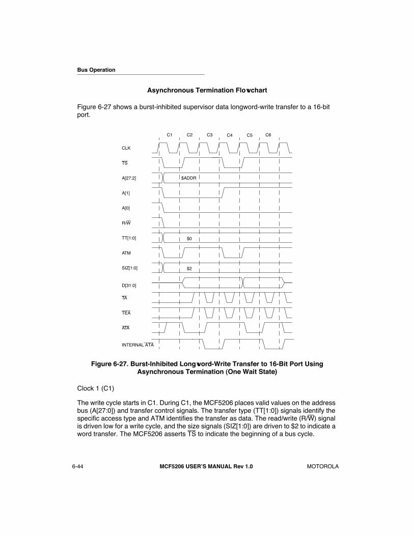
Bus Operation
6-44 MCF5206 USERÕS MANUAL Rev 1.0 MOTOROLA
Asynchronous Termination Flowchart
Figure 6-27 shows a burst-inhibited supervisor data longword-write transfer to a 16-bit port.
Figure 6-27. Burst-Inhibited Longword-Write Transfer to 16-Bit Port Using Asynchronous Termination (One Wait State)
Clock 1 (C1)
The write cycle starts in C1. During C1, the MCF5206 places valid values on the address bus (A[27:0]) and transfer control signals. The transfer type (TT[1:0]) signals identify the specific access type and ATM identifies the transfer as data. The read/write (R/W) signal is driven low for a write cycle, and the size signals (SIZ[1:0]) are driven to $2 to indicate a word transfer. The MCF5206 asserts TS to indicate the beginning of a bus cycle.
TS
A[27:2]
R/W
CLK
TT[1:0]
ATM
ATA
D[31:0]
TEA
SIZ[1:0]
C1 C2
$2
$0
C3 C4
$ADDR
C5 C6
A[1]
A[0]
TA
INTERNAL ATA
Bus Operation
MOTOROLA MCF5206 USERÕS MANUAL Rev 1.0 6-45
Clock 2 (C2)
During C2, the MCF5206 negates TS, drives ATM high to identify the transfer as supervisor and drives the data on the data bus (D[31:0]). The selected device(s) asserts ATA if it is ready to latch the data.
Clock 3 (C3)
At the end of C3, the MCF5206 samples the level of internal asynchronous transfer acknowledge and if it is asserted, terminates the first word transfer. If internal asynchronous transfer acknowledge is asserted, the transfer of the first word is complete. If internal asynchronous transfer acknowledge is negated, the MCF5206 continues to sample internal asynchronous transfer acknowledge and inserts wait states instead of terminating the transfer. The MCF5206 continues to sample internal asynchronous transfer acknowledge until it is asserted. As long as ATA is asserted by the falling edge of C2, the rising edge of C3 asserts the internal asynchronous transfer acknowledge.
Clock 4 (C4)
This clock is identical to C1, except the MCF5206 increments the address to indicate the next word.
Clock 5 (C5)
This clock is identical to C2, except that the data driven corresponds to the second word of data.
Clock 6 (C6)
This clock is identical to C3, except after asynchronous transfer acknowledge is recognized, the MCF5206 three-states the data bus after the next rising edge of CLK.
6.5.12 Termination Tied to GNDIf the MCF5206 is in a system with multiple masters and you require zero wait-state operation, you can tie ATA to GND to achieve zero wait-state operation for nonDRAM transfers. ATA must be used in this case as the MCF5206 can drive TA during external master accesses. When ATA is tied to GND, all nonDRAM transfers follow the timing shown with TA asserted with zero wait states.
If the MCF5206 is the only master in the system, TA and BG can be tied to GND to grant mastership of the external bus to the MCF5206 and achieve zero wait-state operation.
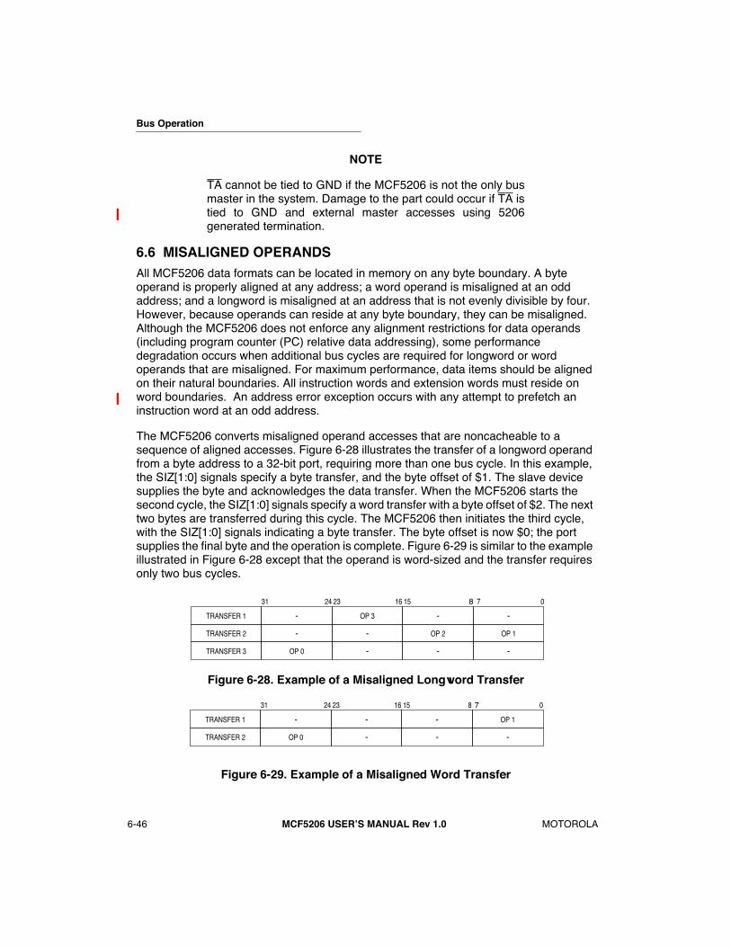
Bus Operation
6-46 MCF5206 USERÕS MANUAL Rev 1.0 MOTOROLA
NOTE
TA cannot be tied to GND if the MCF5206 is not the only busmaster in the system. Damage to the part could occur if TA istied to GND and external master accesses using 5206generated termination.
6.6 MISALIGNED OPERANDSAll MCF5206 data formats can be located in memory on any byte boundary. A byte operand is properly aligned at any address; a word operand is misaligned at an odd address; and a longword is misaligned at an address that is not evenly divisible by four. However, because operands can reside at any byte boundary, they can be misaligned. Although the MCF5206 does not enforce any alignment restrictions for data operands (including program counter (PC) relative data addressing), some performance degradation occurs when additional bus cycles are required for longword or word operands that are misaligned. For maximum performance, data items should be aligned on their natural boundaries. All instruction words and extension words must reside on word boundaries. An address error exception occurs with any attempt to prefetch an instruction word at an odd address.
The MCF5206 converts misaligned operand accesses that are noncacheable to a sequence of aligned accesses. Figure 6-28 illustrates the transfer of a longword operand from a byte address to a 32-bit port, requiring more than one bus cycle. In this example, the SIZ[1:0] signals specify a byte transfer, and the byte offset of $1. The slave device supplies the byte and acknowledges the data transfer. When the MCF5206 starts the second cycle, the SIZ[1:0] signals specify a word transfer with a byte offset of $2. The next two bytes are transferred during this cycle. The MCF5206 then initiates the third cycle, with the SIZ[1:0] signals indicating a byte transfer. The byte offset is now $0; the port supplies the final byte and the operation is complete. Figure 6-29 is similar to the example illustrated in Figure 6-28 except that the operand is word-sized and the transfer requires only two bus cycles.
Figure 6-28. Example of a Misaligned Longword Transfer
Figure 6-29. Example of a Misaligned Word Transfer
TRANSFER 1
TRANSFER 2
TRANSFER 3
-
-
OP 0
OP 3
-
-
-
OP 2
-
-
OP 1
-
31 24 23 16 15 8 7 0
TRANSFER 1
TRANSFER 2
-
OP 0
-
-
-
-
OP 1
-
31 24 23 16 15 8 7 0
Bus Operation
MOTOROLA MCF5206 USERÕS MANUAL Rev 1.0 6-47
NOTE
Alternate masters that are using internal MCF5206 chip-select, DRAM, and default memory control signals mustinitiate aligned transfers only.
6.7 ACKNOWLEDGE CYCLESWhen a peripheral device requires the services of the MCF5206 or is ready to send information that the ColdFire core requires, it can signal the ColdFire core to take an interrupt exception. The interrupt exception transfers control to a routine that responds appropriately. The peripheral device uses the interrupt priority-level/interrupt-request signals (IPLx/IRQx) to signal an interrupt condition to the MCF5206.
The MCF5206 has two levels of interrupt masking. The first level of interrupt masking is in the interrupt controller in the System Integration Module (SIM) which masks individual interrupt inputs and then outputs the interrupt priority level of the highest pending unmasked interrupt to the ColdFire core. The Status Register (SR) provides the second level of interrupt masking in the ColdFire core which contains an interrupt priority mask. The value of the SR interrupt mask is the highest priority level that the ColdFire core ignores. When an interrupt request has a priority higher than the value in the mask, the ColdFire core makes the request a pending interrupt. For more information about the Status Register refer to Section 3.2.2.1 Status Register in the ColdFire Core Section.
The MCF5206 continuously samples the external interrupt input signals and synchronizes and debounces these signals. An interrupt request must be held constant for at least two consecutive CLK periods to be considered a valid input. If the external interrupt inputs are programmed to individual interrupt requests (at levels 1, 4, and 7), the interrupt request must maintain the interrupt request level until the MCF5206 acknowledges the interrupt to guarantee that the interrupt is recognized. If the external interrupt inputs are programmed to be interrupt priority levels, the interrupt request must maintain the interrupt request level or a higher priority level until the MCF5206 acknowledges the interrupt to guarantee that the interrupt is recognized.
NOTE
All interrupts are level sensitive only. Interrupts must remainstable and held valid for the interrupt to be detected.
The MCF5206 takes an interrupt exception for a pending interrupt within one instruction boundary after processing any other pending exception with a higher priority. Thus, the MCF5206 executes at least one instruction in an interrupt exception handler before recognizing another interrupt request.
If the AVEC bit in the Interrupt Control Register (ICR) for the interrupt being acknowledged is set to 1 (enabling autovectoring), the interrupt acknowledge vector is generated internally and no interrupt acknowledge cycle is generated on the external bus. Refer to the SIM section Section 7.3.2.3 Interrupt Control Register (ICR) for ICR programming.

Bus Operation
6-48 MCF5206 USERÕS MANUAL Rev 1.0 MOTOROLA
NOTE
If autovector generation is used for external interrupts, nointerrupt acknowledge cycle is generated on the external bus.Consequently, you must clear the external interrupt in theinterrupt service routine.
6.7.1 Interrupt Acknowledge CycleWhen the MCF5206 processes an interrupt exception, it performs an interrupt acknowledge bus cycle to obtain the vector number that contains the starting location of the interrupt exception handler.
The interrupt acknowledge bus cycle is a read transfer. It differs from a normal read cycle in the following respects:
¥ TT[1:0] = $3 to indicate a CPU space/acknowledge bus cycle
¥ ATM = $1 when TS is asserted and ATM = $0 when TS is negated
¥ Address signals A[27:5] are set to all ones ($7FFFFF)
¥ Address signals A[4:2] are set to the interrupt request level being acknowledged
¥ Address signals A[1:0] are set to all zeros ($0)
The responding device places the vector number on D[31:24] of the data bus during the interrupt acknowledge bus cycle and the cycle is terminated normally with TA or ATA. Figure 6-30 and Figure 6-31 illustrate a flowchart and functional timing diagram for an interrupt-acknowledge cycle terminated with TA.
Figure 6-30. Interrupt-Acknowledge Cycle Flowchart
MCF5206 SYSTEM
1. DRIVE $7FFFFF ON A[27:5]
2. DRIVE $0 ON A[1:0]
3. DRIVE INTERRUPT LEVEL ON A[4:2]
4. DRIVE R/W TO READ (R/W = 1)
5. DRIVE SIZ[1:0] TO INDICATE BYTE (SIZ1 = $0, SIZ0 =$1)
6. DRIVE TT[1:0] AND ATM TO INDICATE INTERRUPT ACKNOWLEDGE (TT[1] = TT[0] = $1 AND ATM = $1)
7. ASSERT TS FOR ONE CLK CYCLE
1. DECODE ADDRESS AND SELECT THE APPROPRIATE SLAVE DEVICE.*
2. DRIVE DATA ON D[31:24]
3. ASSERT TA FOR ONE CLK CYCLE
1. REGISTER DATA (D[31:24])
2. RECOGNIZE THE TRANSFER IS DONE
1. NEGATE TS
2. DRIVE ATM TO INDICATE INTERRUPT ACKNOWLEDGE (ATM = $0)
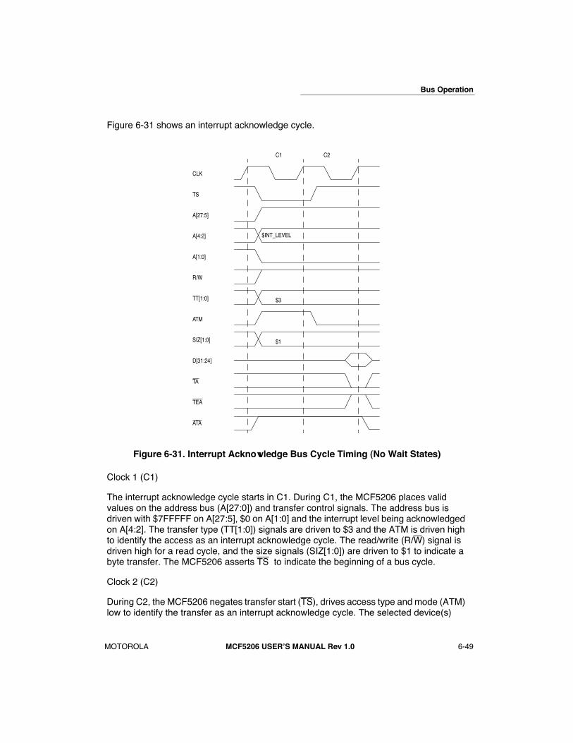
Bus Operation
MOTOROLA MCF5206 USERÕS MANUAL Rev 1.0 6-49
Figure 6-31 shows an interrupt acknowledge cycle.
Figure 6-31. Interrupt Acknowledge Bus Cycle Timing (No Wait States)
Clock 1 (C1)
The interrupt acknowledge cycle starts in C1. During C1, the MCF5206 places valid values on the address bus (A[27:0]) and transfer control signals. The address bus is driven with $7FFFFF on A[27:5], $0 on A[1:0] and the interrupt level being acknowledged on A[4:2]. The transfer type (TT[1:0]) signals are driven to $3 and the ATM is driven high to identify the access as an interrupt acknowledge cycle. The read/write (R/W) signal is driven high for a read cycle, and the size signals (SIZ[1:0]) are driven to $1 to indicate a byte transfer. The MCF5206 asserts TS to indicate the beginning of a bus cycle.
Clock 2 (C2)
During C2, the MCF5206 negates transfer start (TS), drives access type and mode (ATM) low to identify the transfer as an interrupt acknowledge cycle. The selected device(s)
TS
A[27:5]
R/W
CLK
TT[1:0]
ATM
TA
D[31:24]
TEA
SIZ[1:0]
C1 C2
$1
$3
A[4:2] $INT_LEVEL
A[1:0]
ATA

Bus Operation
6-50 MCF5206 USERÕS MANUAL Rev 1.0 MOTOROLA
places the interrupt vector number onto D[31:24] and asserts TA. At the end of C2, the MCF5206 samples the level of TA and if TA is asserted, latches the current value of D[31:24] which contains the interrupt vector number. If TA is asserted, the transfer of the interrupt vector is complete and the transfer terminates. If TA is negated, the MCF5206 continues to sample TA and inserts wait states instead of terminating the transfer. The MCF5206 continues to sample TA on successive rising edges of CLK until it is asserted.
NOTE
Interrupt acknowledge cycles can be asynchronouslyacknowledged using ATA. As long as ATA is asserted by thefalling edge of C2, internal asynchronous transferacknowledge is asserted by the rising edge of C3. Theinterrupt vector must remain driven on D[31:24] until internalasynchronous transfer acknowledge is asserted.
6.8 BUS ERRORSThe system hardware can use the transfer error acknowledge (TEA) signal to abort the current bus cycle when a fault is detected. A bus error is recognized during a bus cycle when TEA is asserted.
When the MCF5206 recognizes a bus error condition for an access, the access is terminated immediately. An access that requires more than one transfer, aborts without completing the remaining transfers if TEA is asserted, regardless of whether the access uses burst or burst-inhibited transfers.

Bus Operation
MOTOROLA MCF5206 USERÕS MANUAL Rev 1.0 6-51
Figure 6-32 shows a bursting supervisor code longword-read access from a 16-bit port with a transfer error.
Figure 6-32. Bursting Longword-Read Access from 16-Bit Port Terminated with TEA Timing
Clock 1 (C1)
The read cycle starts in C1. During C1, the MCF5206 places valid values on the address bus (A[27:0]) and transfer control signals. The transfer type (TT[1:0]) signals identify the specific access type and ATM identifies the transfer as code. The read/write (R/W) signal is driven high for a read cycle, and the size signals (SIZ[1:0]) are driven to $0 to indicate a longword transfer. The MCF5206 asserts transfer start (TS) to indicate the beginning of a bus cycle.
Clock 2 (C2)
During C2, the MCF5206 negates TS and drives ATM high to identify the transfer as supervisor. The selected device detects an error and asserts TEA. At the end of C2, the MCF5206 samples the level of TEA. If it is asserted, the transfer of the longword is aborted and the transfer terminates.
TS
R/W
CLK
TT[1:0]
ATM
TA
D[31:0]
TEA
SIZ[1:0]
C1 C2
$0
$0
A[27:0] $ADDR
ATA
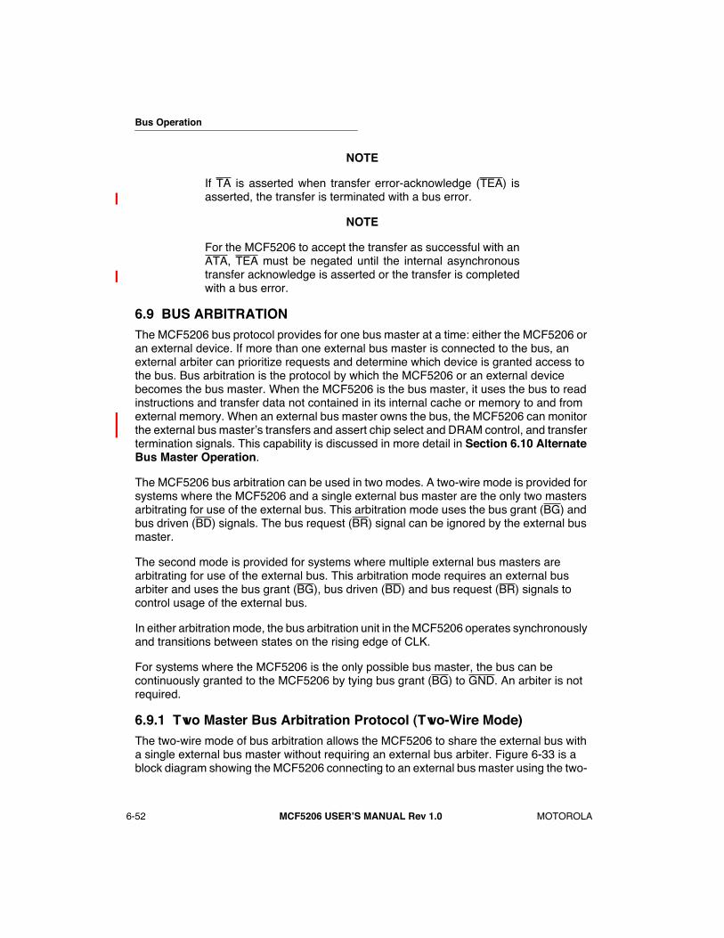
Bus Operation
6-52 MCF5206 USERÕS MANUAL Rev 1.0 MOTOROLA
NOTE
If TA is asserted when transfer error-acknowledge (TEA) isasserted, the transfer is terminated with a bus error.
NOTE
For the MCF5206 to accept the transfer as successful with anATA, TEA must be negated until the internal asynchronoustransfer acknowledge is asserted or the transfer is completedwith a bus error.
6.9 BUS ARBITRATIONThe MCF5206 bus protocol provides for one bus master at a time: either the MCF5206 or an external device. If more than one external bus master is connected to the bus, an external arbiter can prioritize requests and determine which device is granted access to the bus. Bus arbitration is the protocol by which the MCF5206 or an external device becomes the bus master. When the MCF5206 is the bus master, it uses the bus to read instructions and transfer data not contained in its internal cache or memory to and from external memory. When an external bus master owns the bus, the MCF5206 can monitor the external bus masterÕs transfers and assert chip select and DRAM control, and transfer termination signals. This capability is discussed in more detail in Section 6.10 Alternate Bus Master Operation.
The MCF5206 bus arbitration can be used in two modes. A two-wire mode is provided for systems where the MCF5206 and a single external bus master are the only two masters arbitrating for use of the external bus. This arbitration mode uses the bus grant (BG) and bus driven (BD) signals. The bus request (BR) signal can be ignored by the external bus master.
The second mode is provided for systems where multiple external bus masters are arbitrating for use of the external bus. This arbitration mode requires an external bus arbiter and uses the bus grant (BG), bus driven (BD) and bus request (BR) signals to control usage of the external bus.
In either arbitration mode, the bus arbitration unit in the MCF5206 operates synchronously and transitions between states on the rising edge of CLK.
For systems where the MCF5206 is the only possible bus master, the bus can be continuously granted to the MCF5206 by tying bus grant (BG) to GND. An arbiter is not required.
6.9.1 Two Master Bus Arbitration Protocol (Two-Wire Mode)The two-wire mode of bus arbitration allows the MCF5206 to share the external bus with a single external bus master without requiring an external bus arbiter. Figure 6-33 is a block diagram showing the MCF5206 connecting to an external bus master using the two-
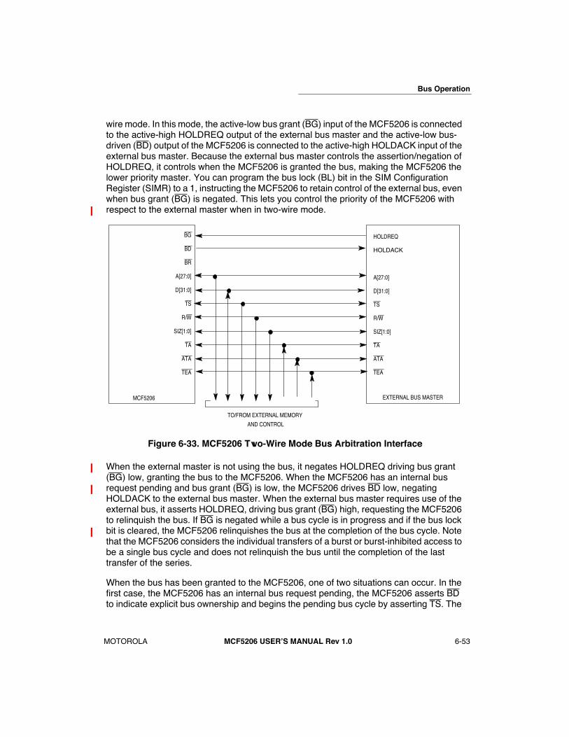
Bus Operation
MOTOROLA MCF5206 USERÕS MANUAL Rev 1.0 6-53
wire mode. In this mode, the active-low bus grant (BG) input of the MCF5206 is connected to the active-high HOLDREQ output of the external bus master and the active-low bus- driven (BD) output of the MCF5206 is connected to the active-high HOLDACK input of the external bus master. Because the external bus master controls the assertion/negation of HOLDREQ, it controls when the MCF5206 is granted the bus, making the MCF5206 the lower priority master. You can program the bus lock (BL) bit in the SIM Configuration Register (SIMR) to a 1, instructing the MCF5206 to retain control of the external bus, even when bus grant (BG) is negated. This lets you control the priority of the MCF5206 with respect to the external master when in two-wire mode.
Figure 6-33. MCF5206 Two-Wire Mode Bus Arbitration Interface
When the external master is not using the bus, it negates HOLDREQ driving bus grant (BG) low, granting the bus to the MCF5206. When the MCF5206 has an internal bus request pending and bus grant (BG) is low, the MCF5206 drives BD low, negating HOLDACK to the external bus master. When the external bus master requires use of the external bus, it asserts HOLDREQ, driving bus grant (BG) high, requesting the MCF5206 to relinquish the bus. If BG is negated while a bus cycle is in progress and if the bus lock bit is cleared, the MCF5206 relinquishes the bus at the completion of the bus cycle. Note that the MCF5206 considers the individual transfers of a burst or burst-inhibited access to be a single bus cycle and does not relinquish the bus until the completion of the last transfer of the series.
When the bus has been granted to the MCF5206, one of two situations can occur. In the first case, the MCF5206 has an internal bus request pending, the MCF5206 asserts BD to indicate explicit bus ownership and begins the pending bus cycle by asserting TS. The
BG
BD
BR
MCF5206
HOLDREQ
HOLDACK
EXTERNAL BUS MASTER
A[27:0]
R/W
SIZ[1:0]
D[31:0]
TS
TA
ATA
TEA
A[27:0]
R/W
SIZ[1:0]
D[31:0]
TS
TA
ATA
TEA
TO/FROM EXTERNAL MEMORY
AND CONTROL

Bus Operation
6-54 MCF5206 USERÕS MANUAL Rev 1.0 MOTOROLA
MCF5206 continues to assert BD until the completion of the bus cycle. If BG is negated by the end of the bus cycle and the Bus Lock bit in the SIMR is 0, the MCF5206 negates BD. As long as BG is asserted, BD remains asserted to indicate the bus is owned by the MCF5206 and the MCF5206 continuously drives the address bus, attributes and control signals.
In the second situation, the bus is granted to the MCF5206, but the MCF5206 does not have an internal bus request pending and the Bus Lock bit in the SIMR is 0, so it takes implicit ownership of the bus. Implicit ownership of the bus occurs when the MCF5206 is granted the bus, but there are no pending bus cycles and the bus lock bit (BL) in the SIMR is set to 0. The MCF5206 does not drive the bus and does not assert bus driven BD if the bus is implicitly owned. If an internal bus request is generated or the bus lock bit in the SIM Configuration Register (SIMR) is set to 1, the MCF5206 assumes explicit ownership of the bus. If explicit ownership was assumed because of an internal request being generated, the MCF5206 immediately begins an access and simultaneously asserts bus driven BD and TS. If explicit ownership was assumed because of the bus lock bit being set to 1, the MCF5206 asserts bus driven BD and drives the address, attributes and control signals but does no assert TS and does not begin a bus transfer.
In the case where the bus lock bit is set to 1, the MCF5206 is the explicit master of the external bus, but does not begin an access until an internal request is generated. Figure6-

Bus Operation
MOTOROLA MCF5206 USERÕS MANUAL Rev 1.0 6-55
34 illustrates implicit and explicit bus ownership because of the bus lock bit being set then an internal bus request being generated.
Figure 6-34. Two-Wire Implicit and Explicit Bus Ownership
In Figure 6-34, the external master has ownership of the external bus during Clock 1 (C1) and Clock 2 (C2). In Clock 3 (C3) the external master releases control of the bus by asserting bus grant (BG) to the MCF5206. During Clock 4 (C4) and Clock 5 (C5) the MCF5206 is implicit owner because an internal access is not pending and the bus lock bit is cleared. In C5, the bus lock bit is set to 1, causing the MCF5206 to take explicit ownership of the bus in Clock 6 (C6) by asserting BD. In Clock 7 (C7) the external master removes the bus grant to the MCF5206. Because the bus lock bit is set to 1, the MCF5206 does not relinquish the bus (the MCF5206 continues to assert BD).
NOTE
The MCF5206 can start a transfer during the CLK cycle afterBG is asserted. The external master should not assert BG tothe MCF5206 until it has stopped driving the bus. BG cannotbe asserted while the external master transfer is still inprogress or damage to the part could occur.
When the bus has been removed from the MCF5206, one of two situations can occur. In the first case, the bus lock bit in the SIM Configuration Register (SIMR) is cleared and the
CLK
TS
TRANSFER
TA
D[31:0]
A[27:0]
ATTRIBUTES
BG
BD
ALTERNATEMASTER MCF5206
BUS LOCK BIT
EXPLICIT OWNERSHIPIMPLICITOWNERSHIP
C1 C2 C3 C4 C5 C6 C7 C8 C9
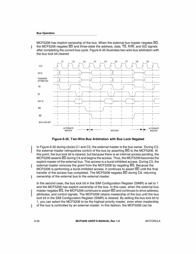
Bus Operation
6-56 MCF5206 USERÕS MANUAL Rev 1.0 MOTOROLA
MCF5206 has implicit ownership of the bus. When the external bus master negates BG, the MCF5206 negates BD and three-state the address, data, TS, R/W, and SIZ signals after completing the current bus cycle. Figure 6-35 illustrates two-wire bus arbitration with the bus lock bit cleared.
Figure 6-35. Two-Wire Bus Arbitration with Bus Lock Negated
In Figure 6-35 during clocks C1 and C2, the external master is the bus owner. During C3, the external master relinquishes control of the bus by asserting BG to the MCF5206. At this point, the bus lock bit is cleared, but because there is an internal access pending, the MCF5206 asserts BD during C4 and begins the access. Thus, the MCF5206 becomes the explicit master of the external bus. This access is a burst-inhibited access. During C5, the external master removes the grant from the MCF5206 by negating BG. Because the MCF5206 is performing a burst-inhibited access, it continues to assert BD until the final transfer of the access has completed. The MCF5206 negates BD during C8, returning ownership of the external bus to the external master.
In the second case, the bus lock bit in the SIM Configuration Register (SIMR) is set to 1 and the MCF5206 has explicit ownership of the bus. In this case, when the external bus master negates BG, the MCF5206 continues to assert BD and continues to drive address, attributes, and control signals. The MCF5206 retains mastership of the bus until the bus lock bit in the SIM Configuration Register (SIMR) is cleared. By setting the bus lock bit to 1, you can select the MCF5206 to be the highest priority master, even when mastership of the bus is controlled by an external master. In this fashion, the MCF5206 can be
CLK
TS
TRANSFER
TA
D[31:0]
A[4:2]
ATTRIBUTES
BG
BD
ALTERNATEMASTER MCF5206
ALTERNATEMASTER
BUS LOCK BIT
C1 C2 C3 C4 C5 C6 C7 C8 C9
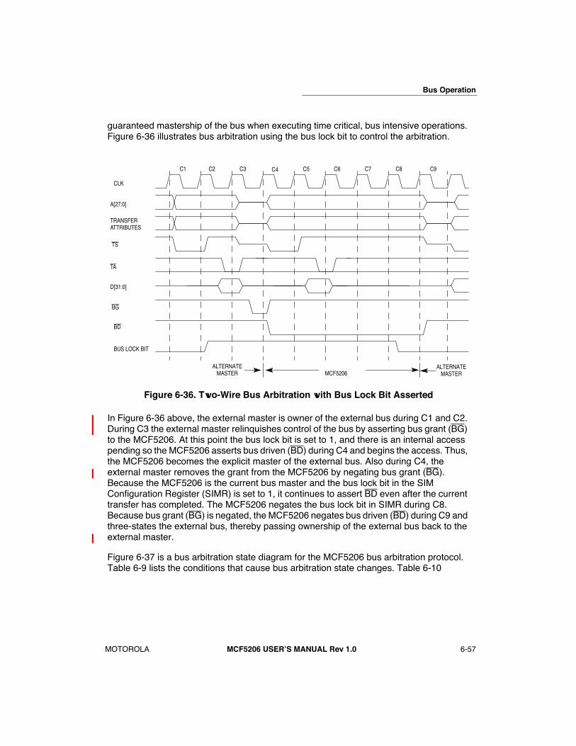
Bus Operation
MOTOROLA MCF5206 USERÕS MANUAL Rev 1.0 6-57
guaranteed mastership of the bus when executing time critical, bus intensive operations. Figure 6-36 illustrates bus arbitration using the bus lock bit to control the arbitration.
Figure 6-36. Two-Wire Bus Arbitration with Bus Lock Bit Asserted
In Figure 6-36 above, the external master is owner of the external bus during C1 and C2. During C3 the external master relinquishes control of the bus by asserting bus grant (BG) to the MCF5206. At this point the bus lock bit is set to 1, and there is an internal access pending so the MCF5206 asserts bus driven (BD) during C4 and begins the access. Thus, the MCF5206 becomes the explicit master of the external bus. Also during C4, the external master removes the grant from the MCF5206 by negating bus grant (BG). Because the MCF5206 is the current bus master and the bus lock bit in the SIM Configuration Register (SIMR) is set to 1, it continues to assert BD even after the current transfer has completed. The MCF5206 negates the bus lock bit in SIMR during C8. Because bus grant (BG) is negated, the MCF5206 negates bus driven (BD) during C9 and three-states the external bus, thereby passing ownership of the external bus back to the external master.
Figure 6-37 is a bus arbitration state diagram for the MCF5206 bus arbitration protocol. Table 6-9 lists the conditions that cause bus arbitration state changes. Table 6-10
CLK
TS
TRANSFER
TA
D[31:0]
A[27:0]
ATTRIBUTES
BG
BD
ALTERNATEMASTER MCF5206
ALTERNATEMASTER
BUS LOCK BIT
C1 C2 C3 C4 C5 C6 C7 C8 C9

Bus Operation
6-58 MCF5206 USERÕS MANUAL Rev 1.0 MOTOROLA
describes the MCF5206 bus ownership, bus driving and assertion of bus driven (BD) for each state of the bus arbitration state machine.
Figure 6-37. MCF5206 Two-Wire Bus Arbitration Protocol State Diagram
Table 6-9. MCF5206 Two-Wire Bus Arbitration Protocol Transition Conditions
PRESENT STATE
CONDITION LABEL
RSTISOFTWARE WATCHDOG
RESETBG
BUS LOCK BIT
INTERNAL BUS REQUEST
TRANSFER IN PROGRESS
END OF CYCLE
NEXT STATE
RESET
A! A - - - - - - ResetA2 N A - - - - - ResetA3 N N N - - - - EM OwnA4 N N A - - - - Implicit Own
IMPLICIT OWN
B1 N N N - - - - EM OwnB2 N N A A - - - Explicit OwnB3 N N A N N - - Implicit OwnB4 N N A N A - - Explicit Own
EXPLICIT OWN
C1 N N A - - - - Explicit OwnC2 N N N A - - - Explicit OwnC3 N N N N - N - EM OwnC4 N N N - - A N Explicit OwnC5 N N N N - A A EM Own
RESET
IMPLICIT
OWN
EXPLICIT
OWN
EM
OWN
A1A2
A3 A4
C3
C1C2
C5
C4
B2
B1
B4
D2D4
D3B3D1

Bus Operation
MOTOROLA MCF5206 USERÕS MANUAL Rev 1.0 6-59
NOTES1)ÒNÓ means negated; ÒAÓ means asserted; ÒEMÓ means external master.
2)End of Cycle: Whatever terminates a bus transaction whether it is normal or bus error. Note that bus cycles that result from a burst inhibited transfer are considered part of that original transfer.
The MCF5206 can be in any one of four arbitration states during bus operation: reset, external master ownership, implicit ownership, or explicit ownership.
The MCF5206 enters the reset state whenever RSTI or software watchdog reset is asserted in any bus arbitration state. When RSTI and the software watchdog reset are negated, the MCF5206 proceeds to the implicit ownership state or external master ownership state, depending on BG.
The external master ownership state denotes the MCF5206 does not have ownership (BG negated) of the bus and the MCF5206 does not drive the bus. The MCF5206 can assert memory control signals (i.e., CS[7:0], WE[3:0], RAS[1:0] or CAS[3:0]) and transfer acknowledge (TA) during this state.
The implicit ownership state indicates that the MCF5206 owns the bus because BG is asserted to it. The MCF5206, however, is not ready to begin a bus cycle and the bus lock bit in the SIM Configuration Register (SIMR) is cleared. In this case, the MCF5206 keeps the bus three-stated until an internal bus request occurs or the bus lock bit in the SIMR is set to 1.
The MCF5206 explicitly owns the bus when the bus is granted to it (BG asserted) and at least one bus cycle has been initiated or the bus lock bit in the SIMR is set to 1. The MCF5206 asserts BD in this state to indicate the MCF5206 has explicit ownership of the bus. Until BG is negated, the MCF5206 retains explicit ownership of the bus whether or not active bus cycles are being executed. Once BG is negated and the bus lock bit in the SIMR is cleared, the MCF5206 relinquishes the bus at the end of the current bus cycle. When the MCF5206 is ready to relinquish the bus, it negates BD and three-states the bus signals.
AM OWN
D1 N N N - - - - EM OwnD2 N N A A - - - Explicit OwnD3 N N A N N - - Implicit OwnD4 N N A N A - - Explictit Own
Table 6-10. MCF5206 Two-Wire Arbitration Protocol State Diagram
STATE OWN BUS STATUS BD
Reset No Not Driven NegatedImplicit Own Yes Not Driven NegatedExplicit Own Yes Driven Asserted
Am Own No Not Driven Negated
Table 6-9. MCF5206 Two-Wire Bus Arbitration Protocol Transition Conditions

Bus Operation
6-60 MCF5206 USERÕS MANUAL Rev 1.0 MOTOROLA
6.9.2 Multiple External Bus Master Arbitration Protocol (Three-Wire Mode)The three-wire mode of bus arbitration allows the MCF5206 to share the external bus with any number of external bus masters. In this mode, an external arbiter must be provided to assign priorities to each of the possible bus masters and determine which master should be allowed use of the external bus. The bus arbitration signals of the MCF5206, BR, BD, and BG connect to the bus arbiter, allowing the bus arbiter to control use of the external bus by the MCF5206.
The MCF5206 requests the bus from the external bus arbiter by asserting bus request (BR) whenever an internal bus request is pending (the ColdFire core requests an access). The MCF5206 continues to assert BR until after the start of the external bus transfer. The MCF5206 can negate BR at any time regardless of the bus grant (BG) status. If the bus is granted to the MCF5206 when an internal bus request is generated, the MCF5206 asserts bus driven (BD) simultaneously with transfer start, allowing the access to begin immediately. The MCF5206 always drives BR and BD. They cannot be directly wire-ORed with other devices.
The external arbiter asserts BG to indicate to the MCF5206 that it has been granted the bus and may begin a bus cycle after the rising edge of the next CLK. If BG is negated while a bus cycle is in progress, the MCF5206 relinquishes the bus at the completion of the bus cycle, except if the bus lock (BL) bit in the SIMR is set. To guarantee that the bus is relinquished, BL must be cleared and BG must be negated prior to the rising edge of the CLK in which the last TA, TEA or internal asynchronous transfer acknowledge is asserted. Note that the MCF5206 considers any series of bus transfers of a burst or a burst-inhibited transfer to be a single bus cycle and does not relinquish the bus until completion of the last transfer of the series.
When the bus has been granted to the MCF5206 in response to the assertion of BR, one of two situations can occur. In the first case, the MCF5206 has an internal bus request pending, the MCF5206 asserts BD to indicate explicit bus ownership and begins the pending bus cycle by asserting TS. The MCF5206 continues to assert BD until the external bus master negates BG, after which BD is negated at the completion of the bus cycle. As long as BG is asserted, BD remains asserted to indicate the bus is owned by the MCF5206 and the MCF5206 continuously drives the address bus, attributes and control signals.
In the second situation, the bus is granted to the MCF5206, but the MCF5206 does not have an internal bus request pending and the bus lock bit in the SIMR is cleared. In this case, the MCF5206 takes implicit ownership of the bus. Implicit ownership of the bus occurs when the MCF5206 is granted the bus, but there are no pending bus cycles. The MCF5206 does not drive the bus and does not assert BD if the bus is implicitly owned. If an internal bus request is generated or the bus lock bit in the SIMR is set to 1, the MCF5206 assumes explicit ownership of the bus. If explicit ownership was assumed due to an internal request being generated, the MCF5206 immediately begins an access and simultaneously asserts BD and TS. If explicit ownership was assumed due to the bus lock
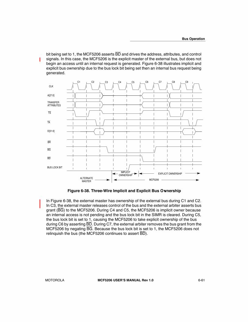
Bus Operation
MOTOROLA MCF5206 USERÕS MANUAL Rev 1.0 6-61
bit being set to 1, the MCF5206 asserts BD and drives the address, attributes, and control signals. In this case, the MCF5206 is the explicit master of the external bus, but does not begin an access until an internal request is generated. Figure 6-38 illustrates implicit and explicit bus ownership due to the bus lock bit being set then an internal bus request being generated.
Figure 6-38. Three-Wire Implicit and Explicit Bus Ownership
In Figure 6-38, the external master has ownership of the external bus during C1 and C2. In C3, the external master releases control of the bus and the external arbiter asserts bus grant (BG) to the MCF5206. During C4 and C5, the MCF5206 is implicit owner because an internal access is not pending and the bus lock bit in the SIMR is cleared. During C5, the bus lock bit is set to 1, causing the MCF5206 to take explicit ownership of the bus during C6 by asserting BD. During C7, the external arbiter removes the bus grant from the MCF5206 by negating BG. Because the bus lock bit is set to 1, the MCF5206 does not relinquish the bus (the MCF5206 continues to assert BD).
CLK
TS
TRANSFER
TA
D[31:0]
A[27:0]
ATTRIBUTES
BG
BD
ALTERNATEMASTER MCF5206
BUS LOCK BIT
EXPLICIT OWNERSHIPIMPLICITOWNERSHIP
BR
C1 C2 C3 C4 C5 C6 C7 C8 C9

Bus Operation
6-62 MCF5206 USERÕS MANUAL Rev 1.0 MOTOROLA
NOTE
The MCF5206 can start a transfer during the CLK cycle afterBG is asserted. The external arbiter should not assert BG tothe MCF5206 until the previous external master has stoppeddriving the bus. BG cannot be asserted while another externalmaster transfer is still in progress or damage to the part couldoccur.
When the bus has been removed from the MCF5206, one of two situations can occur. In the first case, the bus lock bit in the SIMR is cleared and the MCF5206 has explicit ownership of the bus. When the external bus master negates BG, the MCF5206 completes the current transfer, then negate BD and three-state the address, data, TS, R/W, and SIZ signals after completing the current bus cycle.
In the second case, the bus lock bit in the SIMR is set to 1 and the MCF5206 has explicit ownership of the bus. In this case, when the external bus master negates BG, the MCF5206 continues to assert BD and continues to drive address, attributes, and control signals. The MCF5206 retains mastership of the bus until the bus lock bit in the SIMR is cleared. By asserting the bus lock bit, you can select the MCF5206 to be the highest priority master, even when mastership of the bus is controlled by an external arbiter. In this fashion, the MCF5206 can be guaranteed mastership of the bus when executing time-
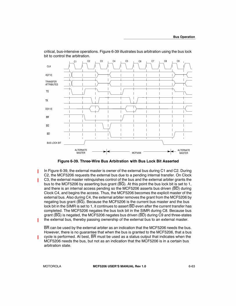
Bus Operation
MOTOROLA MCF5206 USERÕS MANUAL Rev 1.0 6-63
critical, bus-intensive operations. Figure 6-39 illustrates bus arbitration using the bus lock bit to control the arbitration.
Figure 6-39. Three-Wire Bus Arbitration with Bus Lock Bit Asserted
In Figure 6-39, the external master is owner of the external bus during C1 and C2. During C2, the MCF5206 requests the external bus due to a pending internal transfer. On Clock C3, the external master relinquishes control of the bus and the external arbiter grants the bus to the MCF5206 by asserting bus grant (BG). At this point the bus lock bit is set to 1, and there is an internal access pending so the MCF5206 asserts bus driven (BD) during Clock C4, and begins the access. Thus, the MCF5206 becomes the explicit master of the external bus. Also during C4, the external arbiter removes the grant from the MCF5206 by negating bus grant (BG). Because the MCF5206 is the current bus master and the bus lock bit in the SIMR is set to 1, it continues to assert BD even after the current transfer has completed. The MCF5206 negates the bus lock bit in the SIMR during C8. Because bus grant (BG) is negated, the MCF5206 negates bus driven (BD) during C9 and three-states the external bus, thereby passing ownership of the external bus to an external master.
BR can be used by the external arbiter as an indication that the MCF5206 needs the bus. However, there is no guarantee that when the bus is granted to the MCF5206, that a bus cycle is performed. At best, BR must be used as a status output that indicates when the MCF5206 needs the bus, but not as an indication that the MCF5206 is in a certain bus arbitration state.
CLK
TS
TRANSFER
TA
D[31:0]
A[27:0]
ATTRIBUTES
BG
BD
ALTERNATEMASTER MCF5206
ALTERNATEMASTER
BUS LOCK BIT
BR
C1 C2 C3 C4 C5 C6 C7 C8 C9
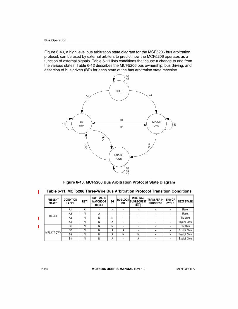
Bus Operation
6-64 MCF5206 USERÕS MANUAL Rev 1.0 MOTOROLA
Figure 6-40, a high level bus arbitration state diagram for the MCF5206 bus arbitration protocol, can be used by external arbiters to predict how the MCF5206 operates as a function of external signals. Table 6-11 lists conditions that cause a change to and from the various states. Table 6-12 describes the MCF5206 bus ownership, bus driving, and assertion of bus driven (BD) for each state of the bus arbitration state machine.
Figure 6-40. MCF5206 Bus Arbitration Protocol State Diagram
Table 6-11. MCF5206 Three-Wire Bus Arbitration Protocol Transition Conditions
PRESENT STATE
CONDITION LABEL
RSTISOFTWARE WATCHDOG
RESETBG
BUS LOCK BIT
INTERNAL BUS REQUEST
(IBR)
TRANSFER IN PROGRESS
END OF CYCLE
NEXT STATE
RESET
A1 A - - - - - - ResetA2 N A - - - - - ResetA3 N N N - - - - EM OwnA4 N N A - - - - Implicit Own
IMPLICIT OWN
B1 N N N - - - - EM OwnB2 N N A A - - - Explicit OwnB3 N N A N N - - Implicit OwnB4 N N A - A - - Explicit Own
RESET
IMPLICIT
OWN
EXPLICIT
OWN
EM
OWN
A1A2
A3 A4
C3
C1C2
C5
C4
B2
B1
B4
D2D4
D3B3D1

Bus Operation
MOTOROLA MCF5206 USERÕS MANUAL Rev 1.0 6-65
NOTES:1)ÒNÓ means negated; ÒAÓ means asserted; ÒEMÓ means external master.2)End of Cycle: Whatever terminates a bus transaction whether it is normal or bus error. Note that bus cycles that
result from a burst inhibited transfer are considered part of that original transfer.
3)IBR refers to an internal bus request.The output signals BR is a registered version of IBR when BG is negated and BD is negated. There is an internal bus request when the ColdÞre core requires the external bus for an operand transfer.
The MCF5206 can be in any one of four arbitration states during bus operation: reset, external master own, implicit ownership, and explicit ownership.
The reset state is entered whenever RSTI or software watchdog reset is asserted in any bus arbitration state. When RSTI and the software watchdog reset are negated, the MCF5206 proceeds to the implicit ownership state or external master ownership state, depending on bus grant (BG).
The external master ownership state denotes the MCF5206 does not have ownership (bus grant (BG) negated) of the bus and the MCF5206 does not drive the bus. The MCF5206 can assert memory control signals (i.e., CS[7:0], WE[3:0], RAS[1:0] or CAS[3:0]) TA and BR during this state.
The implicit ownership state indicates that the MCF5206 owns the bus because bus grant (BG) is asserted to it. The MCF5206, however, is not ready to begin a bus cycle and the bus lock bit in the SIMR is cleared, and it keeps the bus three-stated until an internal bus request occurs or the bus lock bit in the SIMR is set to 1.
The MCF5206 explicitly owns the bus when the bus is granted to it (bus grant (BG) asserted) and at least one bus cycle has initiated or the bus lock bit in the SIMR is set to 1. The MCF5206 asserts BD in this state to indicate the MCF5206 has explicit ownership of the bus. Until bus grant (BG) is negated, the MCF5206 regains explicit ownership of the
EXPLICIT OWN
C1 N N A - - - - Explicit OwnC2 N N N Y - - - Explicit OwnC3 N N N N - N - EM OwnC4 N N N - - Y N Explicit OwnC5 N N N N - Y Y EM Own
EM OWN
D1 N N N - - - - EM OwnD2 N N A A - - - Explicit OwnD3 N N A N N - - Implicit OwnD4 N N A N A - - Explicit Own
Table 6-12. MCF5206 Three-Wire Arbitration Protocol State Diagram
STATE OWN BUS STATUS BD
Reset No Not Driven NegatedImplicit Own Yes Not Driven NegatedExplicit Own Yes Driven Asserted
EM Own No Not Driven Negated
Table 6-11. MCF5206 Three-Wire Bus Arbitration Protocol Transition Conditions

Bus Operation
6-66 MCF5206 USERÕS MANUAL Rev 1.0 MOTOROLA
bus whether or not active bus cycles are being executed. Once bus grant (BG) is negated and the bus lock bit in the SIMR is cleared, the MCF5206 relinquishes the bus at the end of the current bus cycle. When the MCF5206 is ready to relinquish the bus, it negates BD and three-states the bus signals.
The bus arbitration state diagram for the MCF5206 three-wire bus arbitration protocol can be used to approximate the high level behavior of the MCF5206. It is assumed that all TS signals in a system are tied together and each bus masterÕs BD and BR signals are connected individually to the external bus arbiter. The external bus arbiter must be careful to make sure any external bus master has relinquished the bus or is relinquishing the bus after the next rising edge of CLK before asserting bus grant (BG) to the MCF5206. The MCF5206 does not monitor external bus master operation regarding bus arbitration.
NOTE
The MCF5206 can start a transfer on the rising edge of CLKthe cycle after BG is asserted. The external arbiter should notassert BG to the MCF5206 until the previous external masterhas stopped driving the bus. BG cannot be asserted whileanother external master transfer is still in progress or damageto the part could occur.
6.10 ALTERNATE BUS MASTER OPERATIONThe MCF5206 can monitor bus transfers by other bus masters and can assert chip select, DRAM control, and transfer termination signals during these transfers. Assertion of chip- select and DRAM control signals can occur when the bus is granted to another bus master and TS is asserted by the external master as an input to the MCF5206.
NOTE
Alternate masters that are using internal MCF5206 chipselect, DRAM, and default memory control signals mustinitiate aligned transfers only.
The MCF5206 registers the value of A[27:0], R/W, and SIZ[1:0] on the rising edge of CLK in which TS is asserted.
NOTE
If the pins A[27:24]/CS[7:4]/WE[0:3] are not assigned tooutput address signals, a value of $0 is assigned internally toA[27:24]. Also, TT[1:0] and ATM are not examined duringexternal master transfers. The mask bits SC, SD, UC, UD andC/I in the Chip Select Mask Registers (CSMR) and in the
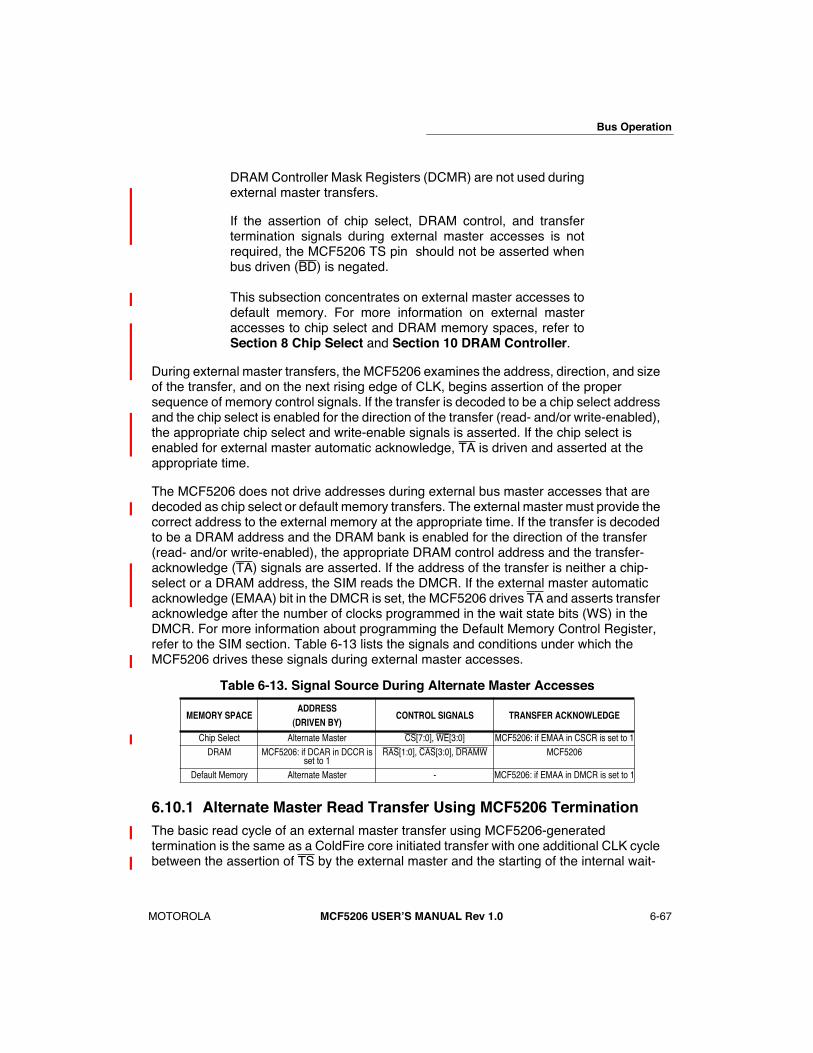
Bus Operation
MOTOROLA MCF5206 USERÕS MANUAL Rev 1.0 6-67
DRAM Controller Mask Registers (DCMR) are not used duringexternal master transfers.
If the assertion of chip select, DRAM control, and transfertermination signals during external master accesses is notrequired, the MCF5206 TS pin should not be asserted whenbus driven (BD) is negated.
This subsection concentrates on external master accesses todefault memory. For more information on external masteraccesses to chip select and DRAM memory spaces, refer toSection 8 Chip Select and Section 10 DRAM Controller.
During external master transfers, the MCF5206 examines the address, direction, and size of the transfer, and on the next rising edge of CLK, begins assertion of the proper sequence of memory control signals. If the transfer is decoded to be a chip select address and the chip select is enabled for the direction of the transfer (read- and/or write-enabled), the appropriate chip select and write-enable signals is asserted. If the chip select is enabled for external master automatic acknowledge, TA is driven and asserted at the appropriate time.
The MCF5206 does not drive addresses during external bus master accesses that are decoded as chip select or default memory transfers. The external master must provide the correct address to the external memory at the appropriate time. If the transfer is decoded to be a DRAM address and the DRAM bank is enabled for the direction of the transfer (read- and/or write-enabled), the appropriate DRAM control address and the transfer- acknowledge (TA) signals are asserted. If the address of the transfer is neither a chip- select or a DRAM address, the SIM reads the DMCR. If the external master automatic acknowledge (EMAA) bit in the DMCR is set, the MCF5206 drives TA and asserts transfer acknowledge after the number of clocks programmed in the wait state bits (WS) in the DMCR. For more information about programming the Default Memory Control Register, refer to the SIM section. Table 6-13 lists the signals and conditions under which the MCF5206 drives these signals during external master accesses.
6.10.1 Alternate Master Read Transfer Using MCF5206 TerminationThe basic read cycle of an external master transfer using MCF5206-generated termination is the same as a ColdFire core initiated transfer with one additional CLK cycle between the assertion of TS by the external master and the starting of the internal wait-
Table 6-13. Signal Source During Alternate Master Accesses
MEMORY SPACEADDRESS
(DRIVEN BY)CONTROL SIGNALS TRANSFER ACKNOWLEDGE
Chip Select Alternate Master CS[7:0], WE[3:0] MCF5206: if EMAA in CSCR is set to 1DRAM MCF5206: if DCAR in DCCR is
set to 1RAS[1:0], CAS[3:0], DRAMW MCF5206
Default Memory Alternate Master - MCF5206: if EMAA in DMCR is set to 1
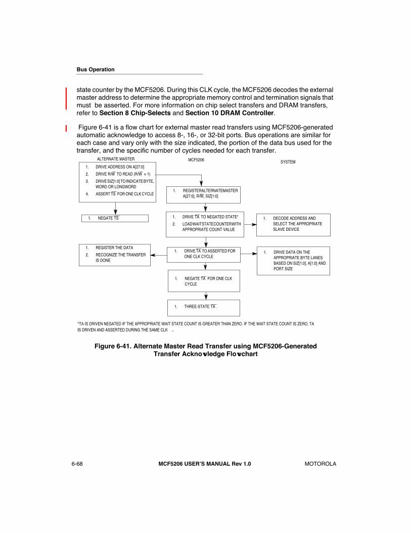
Bus Operation
6-68 MCF5206 USERÕS MANUAL Rev 1.0 MOTOROLA
state counter by the MCF5206. During this CLK cycle, the MCF5206 decodes the external master address to determine the appropriate memory control and termination signals that must be asserted. For more information on chip select transfers and DRAM transfers, refer to Section 8 Chip-Selects and Section 10 DRAM Controller.
Figure 6-41 is a flow chart for external master read transfers using MCF5206-generated automatic acknowledge to access 8-, 16-, or 32-bit ports. Bus operations are similar for each case and vary only with the size indicated, the portion of the data bus used for the transfer, and the specific number of cycles needed for each transfer.
Figure 6-41. Alternate Master Read Transfer using MCF5206-Generated Transfer Acknowledge Flowchart
ALTERNATE MASTER MCF5206
1. DRIVE ADDRESS ON A[27:0]
2. DRIVE R/W TO READ (R/W = 1)
3. DRIVE SIZ[1:0] TO INDICATE BYTE, WORD OR LONGWORD
4. ASSERT TS FOR ONE CLK CYCLE1. REGISTER ALTERNATE MASTER
A[27:0], R/W, SIZ[1:0]
1. NEGATE TS
1. REGISTER THE DATA
2. RECOGNIZE THE TRANSFER IS DONE
1. DRIVE TA TO NEGATED STATE*
2. LOAD WAIT STATE COUNTER WITH APPROPRIATE COUNT VALUE
1. DRIVE TA TO ASSERTED FOR ONE CLK CYCLE
1. NEGATE TA FOR ONE CLK CYCLE
1. DRIVE DATA ON THE APPROPRIATE BYTE LANES BASED ON SIZ[1:0], A[1:0] AND PORT SIZE
SYSTEM
1. DECODE ADDRESS AND SELECT THE APPROPRIATE SLAVE DEVICE
1. THREE-STATE TA .
*TA IS DRIVEN NEGATED IF THE APPROPRIATE WAIT STATE COUNT IS GREATER THAN ZERO. IF THE WAIT STATE COUNT IS ZERO, TAIS DRIVEN AND ASSERTED DURING THE SAME CLK .
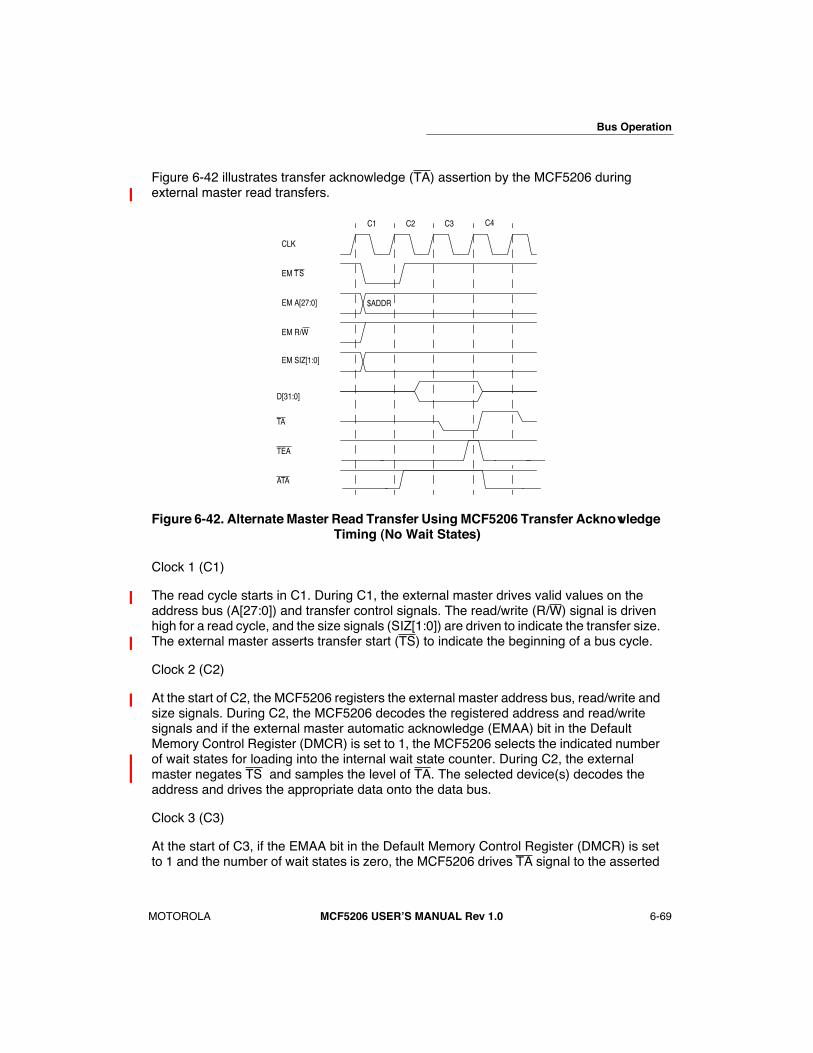
Bus Operation
MOTOROLA MCF5206 USERÕS MANUAL Rev 1.0 6-69
Figure 6-42 illustrates transfer acknowledge (TA) assertion by the MCF5206 during external master read transfers.
Figure 6-42. Alternate Master Read Transfer Using MCF5206 Transfer Acknowledge Timing (No Wait States)
Clock 1 (C1)
The read cycle starts in C1. During C1, the external master drives valid values on the address bus (A[27:0]) and transfer control signals. The read/write (R/W) signal is driven high for a read cycle, and the size signals (SIZ[1:0]) are driven to indicate the transfer size. The external master asserts transfer start (TS) to indicate the beginning of a bus cycle.
Clock 2 (C2)
At the start of C2, the MCF5206 registers the external master address bus, read/write and size signals. During C2, the MCF5206 decodes the registered address and read/write signals and if the external master automatic acknowledge (EMAA) bit in the Default Memory Control Register (DMCR) is set to 1, the MCF5206 selects the indicated number of wait states for loading into the internal wait state counter. During C2, the external master negates TS and samples the level of TA. The selected device(s) decodes the address and drives the appropriate data onto the data bus.
Clock 3 (C3)
At the start of C3, if the EMAA bit in the Default Memory Control Register (DMCR) is set to 1 and the number of wait states is zero, the MCF5206 drives TA signal to the asserted
EM TS
EM A[27:0]
EM R/W
CLK
TA
D[31:0]
EM SIZ[1:0]
C1 C2 C3 C4
TEA
ATA
$ADDR
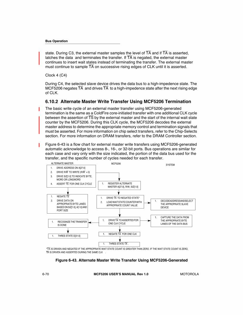
Bus Operation
6-70 MCF5206 USERÕS MANUAL Rev 1.0 MOTOROLA
state. During C3, the external master samples the level of TA and if TA is asserted, latches the data and terminates the transfer. If TA is negated, the external master continues to insert wait states instead of terminating the transfer. The external master must continue to sample TA on successive rising edges of CLK until it is asserted.
Clock 4 (C4)
During C4, the selected slave device drives the data bus to a high-impedence state. The MCF5206 negates TA and drives TA to a high-impedence state after the next rising edge of CLK.
6.10.2 Alternate Master Write Transfer Using MCF5206 TerminationThe basic write cycle of an external master transfer using MCF5206-generated termination is the same as a ColdFire core-initiated transfer with one additional CLK cycle between the assertion of TS by the external master and the start of the internal wait state counter by the MCF5206. During this CLK cycle, the MCF5206 decodes the external master address to determine the appropriate memory control and termination signals that must be asserted. For more information on chip select transfers, refer to the Chip-Selects section. For more information on DRAM transfers, refer to the DRAM Controller section.
Figure 6-43 is a flow chart for external master write transfers using MCF5206-generated automatic acknowledge to access 8-, 16-, or 32-bit ports. Bus operations are similar for each case and vary only with the size indicated, the portion of the data bus used for the transfer, and the specific number of cycles needed for each transfer.
Figure 6-43. Alternate Master Write Transfer Using MCF5206-Generated
ALTERNATE MASTER MCF5206
1. DRIVE ADDRESS ON A[27:0]
2. DRIVE R/W TO WRITE (R/W = 0)
3. DRIVE SIZ[1:0] TO INDICATE BYTE, WORD OR LONGWORD
4. ASSERT TS FOR ONE CLK CYCLE 1. REGISTER ALTERNATE MASTER A[27:0], R/W, SIZ[1:0]
1. NEGATE TS
2. DRIVE DATA ON APPROPRIATE BYTE LANES BASED ON SIZ[1:0], A[1:0] AND PORT SIZE
1. RECOGNIZE THE TRANSFER IS DONE
1. DRIVE TA TO NEGATED STATE*
2. LOAD WAIT STATE COUNTER WITH APPROPRIATE COUNT VALUE
1. NEGATE TA FOR ONE CLK
1. THREE-STATE TA .
1. CAPTURE THE DATA FROM THE APPROPRIATE BYTE LANES OF THE DATA BUS
1. THREE-STATE D[31:0]
SYSTEM
1. DECODE ADDRESS AND SELECT THE APPROPRIATE SLAVE DEVICE
*TA IS DRIVEN AND NEGATED IF THE APPROPRIATE WAIT STATE COUNT IS GREATER THAN ZERO. IF THE WAIT STATE COUNT IS ZERO, TA IS DRIVEN AND ASSERTED DURING THE SAME CLK .
1. DRIVE TA TO ASSERTED FOR ONE CLK CYCLE

Bus Operation
MOTOROLA MCF5206 USERÕS MANUAL Rev 1.0 6-71
Transfer Acknowledge Flowchart
Figure 6-44 illustrates TA assertion by the MCF5206 during external master write transfers.
Figure 6-44. Alternate Master Write Transfer Using MCF5206 Transfer-Acknowledge Timing (No Wait States)
Clock 1 (C1)
The write cycle starts in C1. During C1, the external master drives valid values on the address bus (A[27:0]) and transfer control signals. The read/write (R/W) signal is driven low for a write cycle, and the size signals (SIZ[1:0]) are driven to indicate the transfer size. The external master asserts transfer start (TS) to indicate the beginning of a bus cycle.
Clock 2 (C2)
At the start of C2, the MCF5206 registers and decodes the external master address bus, read/write and size signals. If the external master automatic acknowledge (EMAA) bit in the Default Memory Control Register (DMCR) is set to 1, the MCF5206 selects the indicated number of wait states for loading into the internal wait state counter. During C2, the external master negates TS, places the data on the data bus (D[31:0]), and samples the level of TA. The selected device(s) decode the address and latch the data when it is ready.
Clock 3 (C3)
EM TS
EM A[27:0]
EM R/W
CLK
TA
EM D[31:0]
EM SIZ[1:0]
C1 C2 C3 C4
TEA
ATA
$ADDR

Bus Operation
6-72 MCF5206 USERÕS MANUAL Rev 1.0 MOTOROLA
At the start of C3, if the EMAA bit in the Default Memory Control Register (DMCR) is set to 1 and the number of wait states is zero, the MCF5206 asserts TA . During C3, the external master samples the level of TA. If TA is asserted, the external master terminates the transfer. If TA is negated, the external master continues to output the data and inserts wait states instead of terminating the transfer. The external master must continue to sample TA on successive rising edges of CLK until it is asserted.
Clock 4 (C4)
During C4, the external master places the data bus in a high-impedence state. The MCF5206 negates TA and drives TA to a high impedence state after the next rising edge of CLK.
6.10.3 Alternate Master Bursting Read Using MCF5206-Generated Transfer TerminationThe bursting read transfer of an external master transfer using MCF5206-generated termination is similar to a ColdFire core initiated bursting transfer with the exception that one additional CLK cycle is inserted between the assertion of TS by the external master and the starting of the internal wait state counter by the MCF5206. If the transfer is to default memory, the external master must increment the address to the appropriate value after each assertion of transfer acknowledge. For more information on chip select transfers, refer to Section 8 Chip-Selects. For more information on DRAM transfers, refer to Section 10 DRAM Controller.
NOTE
An external master cannot initiate a bursting read transfer fora chip select or default memory space where the burst-enablebit (BRST) in the Chip Select Control Register (CSCR) or theDefault Memory Control Register (DMCR) is cleared.Undefined behavior occurs if you attempt such a transfer.
Figure 6-45 is a flowchart for an external master bursting read transfer using MCF5206- generated automatic acknowledge to access 8-, 16-, or 32-bit ports. Bus operations are similar for each case and vary only with the size indicated, the portion of the data bus used for the transfer, and the specific number of cycles needed for each transfer. A bursting read transfer can be from 2 to 16 transfers long. The flowchart in Figure 6-45 is for a bursting transfer 4 transfers long.

Bus Operation
MOTOROLA MCF5206 USERÕS MANUAL Rev 1.0 6-73
Figure 6-45. Alternate Master Bursting Read Transfer Using MCF5206-Generated Transfer-Acknowledge Flowchart
ALTERNATE MASTER MCF5206
1. DRIVE ADDRESS ON A[27:0]
2. DRIVE R/W TO READ (R/W = 1)
3. DRIVE SIZ[1:0] TO INDICATE WORD, LONGWORD OR LINE
4. ASSERT TS FOR ONE CLK CYCLE 1. REGISTER ALTERNATE MASTER A[27:0], R/W , SIZ[1:0]
1. NEGATE TS
1. REGISTER DATA
2. RECOGNIZE THE 1ST TRANSFER IS DONE
3. INCREMENT APPROPRIATE ADDRESS BITS BASED ON SIZ[1:0], A[3:0] AND PORT SIZE
1. DRIVE TA TO NEGATED STATE*
2. LOAD WAIT STATE COUNTER WITH APPROPRIATE COUNT VALUE
1. DRIVE TA TO ASSERTED FOR ONE CLK CYCLE
1. NEGATE TA FOR ONE CLK CYCLE
1. THREE-STATE TA .
1. DRIVE DATA ON THE APPROPRIATE BYTE LANES BASED ON SIZ[1:0], A[1:0] AND PORT SIZE
SYSTEM
1. DECODE ADDRESS AND SELECT THE APPROPRIATE SLAVE DEVICE
1. DECODE ADDRESS AND SELECT THE APPROPRIATE SLAVE DEVICE
2. DRIVE DATA ON THE APPROPRIATE BYTE LANES BASED ON SIZ[1:0], A[1:0] AND PORT SIZE
1. DRIVE TA TO ASSERTED FOR ONE CLK CYCLE
1. DECODE ADDRESS AND SELECT THE APPROPRIATE SLAVE DEVICE
2. DRIVE DATA ON THE APPROPRIATE BYTE LANES BASED ON SIZ[1:0], A[1:0] AND PORT SIZE
1. REGISTER DATA
2. RECOGNIZE THE 2ND TRANSFER IS DONE
3. INCREMENT APPROPRIATE ADDRESS BITS BASED ON SIZ[1:0], A[3:0] AND PORT SIZE
1. DRIVE TA TO ASSERTED FOR ONE CLK CYCLE
1. DECODE ADDRESS AND SELECT THE APPROPRIATE SLAVE DEVICE
2. DRIVE DATA ON THE APPROPRIATE BYTE LANES BASED ON SIZ[1:0], A[1:0] AND PORT SIZE
1. REGISTER DATA
2. RECOGNIZE THE 3RD TRANSFER IS DONE
3. INCREMENT APPROPRIATE ADDRESS BITS BASED ON SIZ[1:0], A[3:0] AND PORT SIZE
1. REGISTER DATA
2. RECOGNIZE THE 4TH TRANSFER IS DONE
1. DRIVE TA TO ASSERTED FOR ONE CLK CYCLE
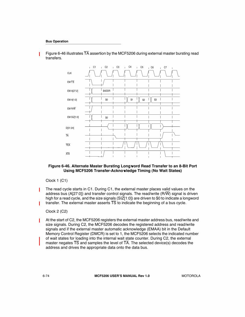
Bus Operation
6-74 MCF5206 USERÕS MANUAL Rev 1.0 MOTOROLA
Figure 6-46 illustrates TA assertion by the MCF5206 during external master bursting read transfers.
Figure 6-46. Alternate Master Bursting Longword Read Transfer to an 8-Bit Port Using MCF5206 Transfer-Acknowledge Timing (No Wait States)
Clock 1 (C1)
The read cycle starts in C1. During C1, the external master places valid values on the address bus (A[27:0]) and transfer control signals. The read/write (R/W) signal is driven high for a read cycle, and the size signals (SIZ[1:0]) are driven to $0 to indicate a longword transfer. The external master asserts TS to indicate the beginning of a bus cycle.
Clock 2 (C2)
At the start of C2, the MCF5206 registers the external master address bus, read/write and size signals. During C2, the MCF5206 decodes the registered address and read/write signals and if the external master automatic acknowledge (EMAA) bit in the Default Memory Control Register (DMCR) is set to 1, the MCF5206 selects the indicated number of wait states for loading into the internal wait state counter. During C2, the external master negates TS and samples the level of TA. The selected device(s) decodes the address and drives the appropriate data onto the data bus.
EM TS
EM A[27:2]
EM R/W
CLK
TA
D[31:24]
EM SIZ[1:0]
C1 C2 C3 C4 C5 C6 C7
$ADDR
EM A[1:0] $0
$0
$1 $2 $3
TEA
ATA
Bus Operation
MOTOROLA MCF5206 USERÕS MANUAL Rev 1.0 6-75
Clock 3 (C3)
At the start of C3, if the EMAA bit in the Default Memory Control Register (DMCR) is set to 1 and the number of wait states is zero, the MCF5206 drives TA signal to the asserted state. During C3, the external master samples the level of TA. If TA is asserted, the external master latches the first byte of data from D[31:24]. If TA is negated, the external master continues to insert wait states instead of terminating the transfer. The external master must continue to sample TA on successive rising edges of CLK until it is asserted.
Clock 4 (C4)
During C4, the external master increments the address by one to access the second byte of data in the longword transfer. The external master also samples the level of TA. If TA is asserted, the external master latches the second byte of data from D[31:24]. If TA is negated, the external master continues to insert wait states instead of terminating the transfer. The external master must continue to sample TA on successive rising edges of CLK until it is asserted.
The selected slave decodes the address and outputs the next byte of data on D[31:24]. The MCF5206 continues to assert TA.
Clock 5 (C5)
This clock is identical to C4, except the external master increments the address to point to the third byte of data, and the selected slave decodes the address and outputs the third byte of data of the longword transfer.
Clock 6 (C6)
This clock is identical to C4, except the external master increments the address to point to the fourth byte of data, and the selected slave decodes the address and outputs the fourth byte of data of the longword transfer.
Clock 7 (C7)
During C7, the selected slave device drives the data bus to a high impedence state. The MCF5206 drives TA to the inactive state and then drives TA to a high-impedence state after the next rising edge of CLK.
6.10.4 Alternate Master Bursting Write Using MCF5206-Generated Transfer TerminationThe bursting write transfer of an external master using MCF5206-generated termination is similar to a ColdFire core initiated bursting write transfer except that one additional CLK cycle is inserted between the assertion of TS by the external master and the start of the internal wait state counter by the MCF5206. If the transfer is to default memory, the external master must increment the address to the appropriate value after each assertion
Bus Operation
6-76 MCF5206 USERÕS MANUAL Rev 1.0 MOTOROLA
of transfer acknowledge. For more information on chip select transfers or DRAM transfers, refer to Section 8 Chip-Selects or to Section 10 DRAM Controller.
NOTE
An external master cannot initiate a bursting write transfer fora chip select or default memory space where the burst-enablebit (BRST) in the Chip Select Control Register (CSCR) or theDefault Memory Control Register (DMCR) is cleared.Undefined behavior occurs if you try this.
Figure 6-47 is a flowchart for external master bursting write transfer using MCF5206 generated automatic acknowledge to access 8-, 16- or 32-bit ports. Bus operations are similar for each case and vary only with the size indicated, the portion of the data bus used for the transfer and the specific number of cycles needed for each transfer. A bursting write transfer can be from two to sixteen transfers long. The flowchart shown in Figure 6-47 is for a bursting write transfer of four transfers long.
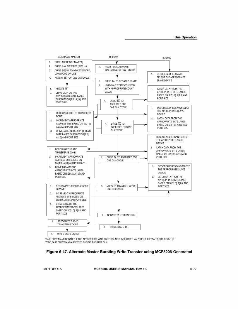
Bus Operation
MOTOROLA MCF5206 USERÕS MANUAL Rev 1.0 6-77
Figure 6-47. Alternate Master Bursting Write Transfer using MCF5206-Generated
ALTERNATE MASTER MCF5206
1. DRIVE ADDRESS ON A[27:0]
2. DRIVE R/W TO WRITE (R/W = 0)
3. DRIVE SIZ[1:0] TO INDICATE WORD, LONGWORD OR LINE
4. ASSERT TS FOR ONE CLK CYCLE
1. REGISTER ALTERNATE MASTER A[27:0], R/W , SIZ[1:0]
1. NEGATE TS
2. DRIVE DATA ON THE APPROPRIATE BYTE LANES BASED ON SIZ[1:0], A[1:0] AND PORT SIZE
1. RECOGNIZE THE 1ST TRANSFER IS DONE
2. INCREMENT APPROPRIATE ADDRESS BITS BASED ON SIZ[1:0], A[3:0] AND PORT SIZE
3. DRIVE DATA ON THE APPROPRIATE BYTE LANES BASED ON SIZ[1:0], A[1:0] AND PORT SIZE
1. DRIVE TA TO NEGATED STATE*
2. LOAD WAIT STATE COUNTER WITH APPROPRIATE COUNT VALUE
1. DRIVE TA TO ASSERTED FOR ONE CLK CYCLE
1. NEGATE TA FOR ONE CLK
1. THREE-STATE TA .
1. LATCH DATA FROM THE APPROPRIATE BYTE LANES BASED ON SIZ[1:0], A[1:0] AND PORT SIZE
SYSTEM
1. DECODE ADDRESS AND SELECT THE APPROPRIATE SLAVE DEVICE
1. DECODE ADDRESS AND SELECT THE APPROPRIATE SLAVE DEVICE
2. LATCH DATA FROM THE APPROPRIATE BYTE LANES BASED ON SIZ[1:0], A[1:0] AND PORT SIZE
1. DRIVE TA TO ASSERTED FOR ONE CLK CYCLE
1. DRIVE TA TO ASSERTED FOR ONE CLK CYCLE
1. RECOGNIZE THE 2ND TRANSFER IS DONE
2. INCREMENT APPROPRIATE ADDRESS BITS BASED ON SIZ[1:0], A[3:0] AND PORT SIZE
3. DRIVE DATA ON THE APPROPRIATE BYTE LANES BASED ON SIZ[1:0], A[1:0] AND PORT SIZE
1. DECODE ADDRESS AND SELECT THE APPROPRIATE SLAVE DEVICE
2. LATCH DATA FROM THE APPROPRIATE BYTE LANES BASED ON SIZ[1:0], A[1:0] AND PORT SIZE
1. RECOGNIZE THE 3RD TRANSFER IS DONE
2. INCREMENT APPROPRIATE ADDRESS BITS BASED ON SIZ[1:0], A[3:0] AND PORT SIZE
3. DRIVE DATA ON THE APPROPRIATE BYTE LANES BASED ON SIZ[1:0], A[1:0] AND PORT SIZE
1. DECODE ADDRESS AND SELECT THE APPROPRIATE SLAVE DEVICE
2. LATCH DATA FROM THE APPROPRIATE BYTE LANES BASED ON SIZ[1:0], A[1:0] AND PORT SIZE1. DRIVE TA TO ASSERTED FOR
ONE CLK CYCLE
1. RECOGNIZE THE 4TH TRANSFER IS DONE
*TA IS DRIVEN AND NEGATED IF THE APPROPRIATE WAIT STATE COUNT IS GREATER THAN ZERO. IF THE WAIT STATE COUNT IS ZERO, TA IS DRIVEN AND ASSERTED DURING THE SAME CLK.
1. THREE-STATE D[31:0]

Bus Operation
6-78 MCF5206 USERÕS MANUAL Rev 1.0 MOTOROLA
Transfer-Acknowledge Flowchart
Figure 6-48 illustrates TA assertion by the MCF5206 during external master bursting write transfers.
Figure 6-48. Alternate Master Bursting Longword Write Transfer to a 16-Bit Port Using MCF5206 Transfer Acknowledge Timing (No Wait States)
Clock 1 (C1)
The write cycle starts in C1. During C1, the external master places valid values on the address bus (A[27:0]) and transfer control signals. The read/write (R/W) signal is driven low for a write cycle, and the size signals (SIZ[1:0]) are driven to $0 to indicate a longword transfer. The external master asserts TS to indicate the beginning of a bus cycle.
Clock 2 (C2)
At the start of C2, the MCF5206 registers and decodes the external master address bus, read/write and size signals. If the external master automatic acknowledge (EMAA) bit in the Default Memory Control Register (DMCR) is set to 1, the MCF5206 selects the indicated number of wait states for loading into the internal wait state counter. During C2, the external master negates TS, drives the appropriate data onto the data bus, and
EM TS
EM A[27:2]
EM R/W
CLK
TA
EM D[31:16]
EM SIZ[1:0]
C1 C2 C3 C4 C5
$ADDR
EM A[1]
$0
EM A[0]
TEA
ATA
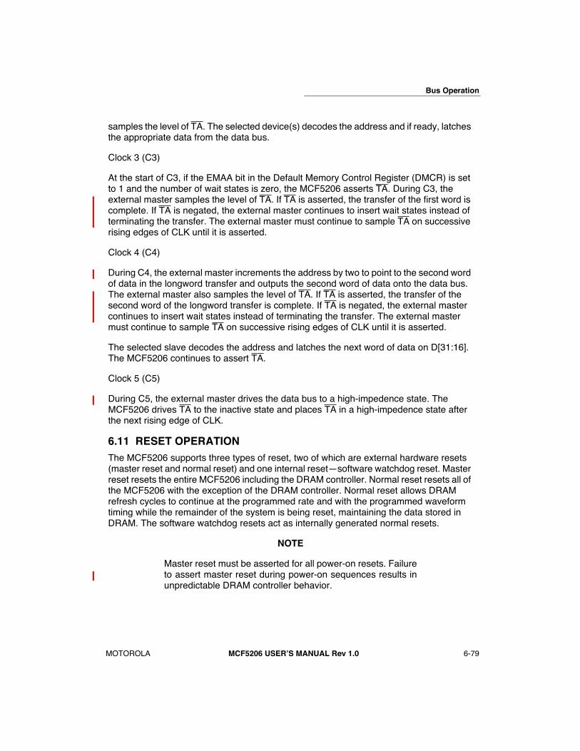
Bus Operation
MOTOROLA MCF5206 USERÕS MANUAL Rev 1.0 6-79
samples the level of TA. The selected device(s) decodes the address and if ready, latches the appropriate data from the data bus.
Clock 3 (C3)
At the start of C3, if the EMAA bit in the Default Memory Control Register (DMCR) is set to 1 and the number of wait states is zero, the MCF5206 asserts TA. During C3, the external master samples the level of TA. If TA is asserted, the transfer of the first word is complete. If TA is negated, the external master continues to insert wait states instead of terminating the transfer. The external master must continue to sample TA on successive rising edges of CLK until it is asserted.
Clock 4 (C4)
During C4, the external master increments the address by two to point to the second word of data in the longword transfer and outputs the second word of data onto the data bus. The external master also samples the level of TA. If TA is asserted, the transfer of the second word of the longword transfer is complete. If TA is negated, the external master continues to insert wait states instead of terminating the transfer. The external master must continue to sample TA on successive rising edges of CLK until it is asserted.
The selected slave decodes the address and latches the next word of data on D[31:16]. The MCF5206 continues to assert TA.
Clock 5 (C5)
During C5, the external master drives the data bus to a high-impedence state. The MCF5206 drives TA to the inactive state and places TA in a high-impedence state after the next rising edge of CLK.
6.11 RESET OPERATIONThe MCF5206 supports three types of reset, two of which are external hardware resets (master reset and normal reset) and one internal resetÑsoftware watchdog reset. Master reset resets the entire MCF5206 including the DRAM controller. Normal reset resets all of the MCF5206 with the exception of the DRAM controller. Normal reset allows DRAM refresh cycles to continue at the programmed rate and with the programmed waveform timing while the remainder of the system is being reset, maintaining the data stored in DRAM. The software watchdog resets act as internally generated normal resets.
NOTE
Master reset must be asserted for all power-on resets. Failureto assert master reset during power-on sequences results inunpredictable DRAM controller behavior.
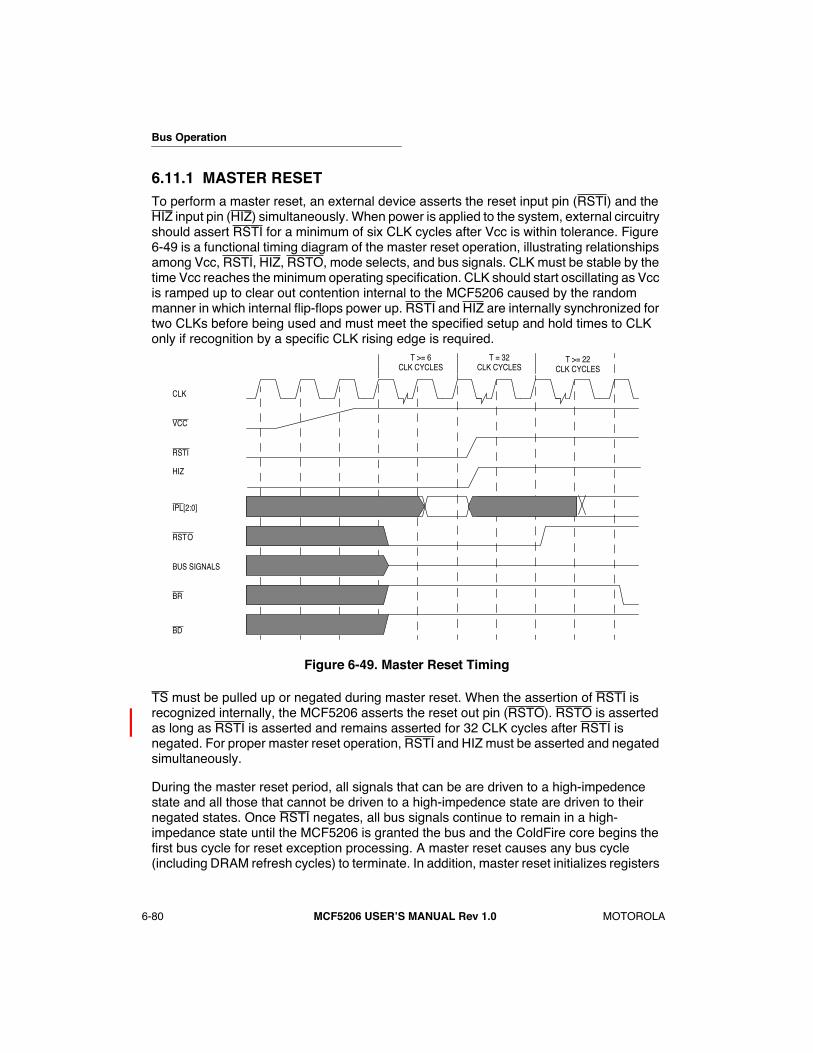
Bus Operation
6-80 MCF5206 USERÕS MANUAL Rev 1.0 MOTOROLA
6.11.1 MASTER RESETTo perform a master reset, an external device asserts the reset input pin (RSTI) and the HIZ input pin (HIZ) simultaneously. When power is applied to the system, external circuitry should assert RSTI for a minimum of six CLK cycles after Vcc is within tolerance. Figure 6-49 is a functional timing diagram of the master reset operation, illustrating relationships among Vcc, RSTI, HIZ, RSTO, mode selects, and bus signals. CLK must be stable by the time Vcc reaches the minimum operating specification. CLK should start oscillating as Vcc is ramped up to clear out contention internal to the MCF5206 caused by the random manner in which internal flip-flops power up. RSTI and HIZ are internally synchronized for two CLKs before being used and must meet the specified setup and hold times to CLK only if recognition by a specific CLK rising edge is required.
Figure 6-49. Master Reset Timing
TS must be pulled up or negated during master reset. When the assertion of RSTI is recognized internally, the MCF5206 asserts the reset out pin (RSTO). RSTO is asserted as long as RSTI is asserted and remains asserted for 32 CLK cycles after RSTI is negated. For proper master reset operation, RSTI and HIZ must be asserted and negated simultaneously.
During the master reset period, all signals that can be are driven to a high-impedence state and all those that cannot be driven to a high-impedence state are driven to their negated states. Once RSTI negates, all bus signals continue to remain in a high-impedance state until the MCF5206 is granted the bus and the ColdFire core begins the first bus cycle for reset exception processing. A master reset causes any bus cycle (including DRAM refresh cycles) to terminate. In addition, master reset initializes registers
VCC
RSTI
IPL[2:0]
CLK
RSTO
BUS SIGNALS
BD
BR
T >= 6CLK CYCLES
T = 32CLK CYCLES
T >= 22CLK CYCLES
HIZ
Bus Operation
MOTOROLA MCF5206 USERÕS MANUAL Rev 1.0 6-81
appropriately for a reset exception. During a master reset, the hard reset bit (HRST) bit in the Reset Status Register (RSR) is set and the software reset bit (SRST) in the RSR is cleared to indicate that an external hardware reset caused the previous reset.
The levels of the IPLx pins select the port size and acknowledge features of the global chip select after a master reset occurs. The IPLx signals are synchronized and are registered on the last rising edge of CLK where RSTI and HIZ are asserted.
6.11.2 NORMAL RESETExternal normal resets should be performed anytime it is important to maintain the data stored in DRAM during a reset. An external normal reset is performed when an external device asserts the reset input pin (RSTI) while negating the HIZ input pin (HIZ). During an external normal reset, RSTI must be asserted for a minimum of six CLKs. Figure 6-50 is a functional timing diagram of external normal reset operation, illustrating relationships among RSTI, HIZ, RSTO, mode selects, and bus signals. RSTI and HIZ are internally synchronized for two CLKs before being used and must meet the specified setup and hold times to CLK only if recognition by a specific CLK rising edge is required.
Figure 6-50. Normal Reset Timing
TS must be pulled up or negated during normal reset. When the assertion of RSTI is recognized internally, the MCF5206 asserts the reset out pin (RSTO). RSTO is asserted as long as RSTI is asserted and remains asserted for 32 CLK cycles after RSTI is negated. For proper normal reset operation, HIZ must be negated as long as RSTI is asserted.
VCC
RSTI
IPL[2:0]
CLK
RSTO
BUS SIGNALS
BD
BR
T >= 6CLK CYCLES
T = 32CLK CYCLES
T >= 22CLK CYCLES
HIZ

Bus Operation
6-82 MCF5206 USERÕS MANUAL Rev 1.0 MOTOROLA
During the normal reset period, all signals that can be are driven to a high-impedence state and all those that cannot are driven to their negated states. Once RSTI negates, all bus signals continue to remain in a high-impedance state until the MCF5206 is granted the bus and the ColdFire core begins the first bus cycle for reset exception processing.
A normal reset causes all bus activity except DRAM refresh cycles to terminate. During a normal reset, DRAM refresh cycles continue to occur at the programmed rate and with the programmed waveform timing. In addition, normal reset initializes registers appropriately for a reset exception. During an external normal reset, the hard reset (HRST) bit in the Reset Status Register (RSR) is set and the software reset (SRST) bit in the Reset Status Register (RSR) is cleared to indicate an external hardware reset caused the previous reset.
The levels of the IPLx pins select the port size and acknowledge features of the global chip select after an external normal reset occurs. The IPLx signals are synchronized and are registered on the last rising edge of CLK where RSTI is asserted.
6.11.3 SOFTWARE WATCHDOG TIMER RESET OPERATIONIf the software watchdog timer is programmed to generate a reset, when a timeout occurs an internal reset is asserted for at least 31 CLKs, resetting internal registers as with a normal reset. The RSTO pin asserts for at least 31 CLKs after the software watchdog timeout. Figure 6-51 illustrates the timing of RSTO when asserted by a software watchdog timeout.
Figure 6-51. Software Watchdog Timer Reset Timing
NOTE
Like the normal reset, the internal reset generated by asoftware watchdog timeout does not reset the DRAM
CLK
RSTO
BUS SIGNALS
BD
BR
T >= 22CLK CYCLES
SOFTWARE
INTERNAL
WATCHDOGTIMEOUT
RESET
T >= 31CLK CYCLES
Bus Operation
MOTOROLA MCF5206 USERÕS MANUAL Rev 1.0 6-83
controller. DRAM refreshes continue to be generated duringand after the software watchdog timout reset at theprogrammed rate and with the programmed waveform timing.
TS must be pulled up or negated during software watchdog reset. When the software watchdog timeout recognized internally, the reset out pin (RTS2/RSTO) is asserted by the MCF5206. RSTO is asserted for at least 31 CLK cycles after the internal software watchdog timer reset negated.
During the software watchdog timer reset period, all signals that can be are driven to a high-impedence state and all those that cannot are driven to their negated states. Once RSTO negates, all bus signals continue to remain in a high-impedance state until the MCF5206 is granted the bus and the ColdFire core begins the first bus cycle for reset exception processing.
A software watchdog timer reset causes all bus activity except DRAM refresh cycles to terminate. During a software watchdog timer reset, DRAM refresh cycles continues to occur at the programmed rate and with the programmed waveform timing. In addition, software watchdog timer reset initializes registers appropriately for a reset exception. During a software watchdog timer reset, the hard reset (HRST) bit in the RSR is cleared and the software reset (SRST) bit in the RSR is set to 1 to indicate that a software watchdog timeout caused the previous reset.
NOTE
The levels of the IPLx pins are not sampled during a softwarewatchdog reset. If the port size and acknowledge features ofthe global chip select are different from the valuesprogrammed in the Chip Select Control Register 0 (CSCR0) atthe time of the software watchdog reset, you must assert RSTIduring software watchdog reset to cause the IPLx/IRQx pinsto be resampled.
2
3
4
5
6
7
8
9
10
11
12
13
14
15
16
1
MOTOROLA
MCF5206 USERÕS MANUAL Rev 1.0
7-1
2
3
4
5
6
7
8
9
10
11
12
13
14
15
16
1
SECTION 7SYSTEM INTEGRATION MODULE
7.1 INTRODUCTION
This subsection details the operation and programming model of the System Integration Module (SIM) registers, including the interrupt controller and system-protection functions for the MCF5206. The SIM provides overall control of the internal and external buses and serves as the interface between the ColdFire core processor and the internal peripherals or external devices.
7.1.1 Features
The following list summarizes the key SIM features:
¥ Module Base Address Register (MBAR)
Ñ Base address location of all internal peripherals and SIM resourcesÑ Address space masking to internal peripherals and SIM resources
¥ Interrupt Controller
Ñ Programmable interrupt level (1-7) for internal peripheral interruptsÑ Programmable priority level (0-3) within each interrupt levelÑ Three external interrupts - programmable as individual interrupt requests or as
interrupt priority-level signals
¥ System Protection
Ñ Reset status to indicate cause of last resetÑ Bus monitor and Spurious Interrupt MonitorÑ Software Watchdog Timer
7.2 SIM OPERATION
7.2.1 Module Base Address Register (MBAR)
The MBAR determines the base address of all internal peripherals as well as the definition of which types of accesses are allowed for these registers.
The MBAR is a 32-bit write-only supervisor control register that physically resides in the SIM. It is accessed in the CPU address space $C0F via the MOVEC instruction. (Refer to the
ColdFire Microprocessor Family ProgrammerÕs Reference Manual
for use of MOVEC instruction). The MBAR can be read when in debug mode using background debug commands.
DATE: 1-9-98
REVISION NO.: 1.1
PAGES AFFECTED: SEE CHANGE BARS

System Integration Module
2
3
4
5
6
7
8
9
10
11
12
13
14
15
16
1
System Integration Module
7-2
MCF5206 USERÕS MANUAL Rev 1.0
MOTOROLA
2
3
4
5
6
7
8
9
10
11
12
13
14
15
16
1
At system reset, the MBAR valid bit is cleared to prevent incorrect references to resources before the MBAR is written. The remainder of the MBAR bits are uninitialized. To access the internal peripherals, you should write MBAR with the appropriate base address and set the valid bit after system reset.
All internal peripheral registers occupy a single relocatable memory block along 1-kbyte boundaries. If the MBAR valid bit is set, the base address field is compared to the upper 22 bits of the full 32-bit internal address to determine if an internal peripheral is being accessed. The MBAR masks specific address spaces using the address space fields. Any attempt to access a masked address space results in an access being generated on the external bus.
7.2.2 Bus Time-Out Monitor
The bus monitor ensures that each external cycle terminates within a programmed period of time. It continually checks the external bus for termination and asserts the internal transfer error acknowledge that results in an access fault exception if the response time is greater than the programmed bus monitor time. If a transfer is in progress while TEA is asserted, the transfer is aborted and the exception occusr.
You can program the bus monitor time to 128, 256, 512, or 1024 clock cycles using the bus monitor timing bits in the system protection control register (SYPCR). The value you select should be larger than the longest possible response time of the slowest peripheral of the system. The bus time-out monitor begins counting on the clock cycle TS is asserted and stops counting on the clock after the assertion of the final transfer termination signal (i.e., for a line transfer to a 32-bit port, the bus time-out monitor starts counting on the clock TS is asserted and stops counting after TA and/or ATA have been asserted a total of four times).
The bus monitor enable bit in the SYPCR enables the bus monitor for external bus cycles. The bus monitor cannot be disabled for internal bus cycles to internal peripherals. Once the SYPCR is written using the MOVEC instruction, the state of the bus time-out monitor cannot be changedÑthe SYPCR may be written only once. Refer to subsection
7.3.2.7 System Protection Control Register (SYPCR)
for programming information.
7.2.3 Spurious Interrupt Monitor
The SIM automatically generates the spurious interrupt vector number 24 ($18), which causes the ColdFire core processor to terminate the cycle with a spurious interrupt exception if:
¥ An external device responds to an interrupt acknowledge cycle by asserting TEA
¥ No interrupt is pending for the interrupt level being acknowledged when the interrupt acknowledge cycle is generated
NOTE
If an external device does not respond to an interruptacknowledge cycle by asserting TA or ATA, an access errorexception is generated, not a spurious interrupt exception. To
System Integration Module
2
3
4
5
6
7
8
9
10
11
12
13
14
15
16
1
System Integration Module
MOTOROLA
MCF5206 USERÕS MANUAL Rev 1.0
7-3
2
3
4
5
6
7
8
9
10
11
12
13
14
15
16
1
generate a spurious interrupt exception, TEA would have to begenerated.
7.2.4 Software Watchdog Timer
The software watchdog timer (SWT) prevents system lockup in case the software becomes trapped in loops with no controlled exit. The SWT can be enabled via the software watchdog enable bit in the SYPCR. If enabled, the SWT requires a special service sequence execution on a periodic basis. If this periodic servicing action does not occur, the SWT times out and results in a hardware reset or a level 7 interrupt, as programmed by the software watchdog reset/interrupt select bit in the SYPCR. If the SWT times out and is programmed to generate a hardware reset, an internal reset is generated and the software watchdog timer reset bit in the reset status register is set. Additionally, if the RTS2/RSTO pin is programmed for RSTO, RSTO is asserted for 32 CLK cycles. Refer to subsection
7.3.2.10 Pin Assignment Register (PAR)
for more information on programming. Also refer to the ColdFire WWW home page at http://www.mot.com/SPS/HPESD/prod/coldfire/MCF5206.html (Product Information Section) for samples of initialization code.
The 8-bit interrupt vector for the SWT interrupt is stored in the software watchdog interrupt vector register (SWIVR). The software watchdog prescalar (SWP) and software watchdog timing (SWT) bits in SYPCR determine the SWT time-out period.
The SWT service sequence consists of these two steps: write $55 to SWSR, then write $AA to the SWSR. Both writes must occur in the order listed prior to the SWT time-out, but any number of instructions or accesses to the SWSR can be executed between the two writes. This order allows interrupts and exceptions to occur, if necessary, between the two writes.
NOTE
If the SYSPCR is programmed for the SWT to generate aninterrupt and the SWT times out, the SWT must be serviced inthe interrupt handler routine by writing the $55, $AA sequenceto the SWSR.
7.2.5 Interrupt Controller
The SIM provides a centralized interrupt controller for all MCF5206 interrupt sources, including:
¥ External Interrupts (IPL/IRQ)
¥ Software watchdog timer
¥ Timer modules
¥ MBUS (I
2
C) module
¥ UART modules
All interrupt inputs are level sensitive. An interrupt request must be held valid for at least two consecutive CLK periods to be considered a valid input. The three external interrupt inputs

System Integration Module
2
3
4
5
6
7
8
9
10
11
12
13
14
15
16
1
System Integration Module
7-4
MCF5206 USERÕS MANUAL Rev 1.0
MOTOROLA
2
3
4
5
6
7
8
9
10
11
12
13
14
15
16
1
can be programmed to be three individual interrupt inputs (at levels 1, 4, and 7) or encoded interrupt priority levels.
NOTE
If the external interrupt inputs are programmed to individualinterrupt requests (at levels 1, 4, and 7), the interrupt requestmust be asserted until the MCF5206 acknowledges the interrupt(by generating an interrupt acknowledge cycle) to guaranteethat the interrupt is recognized.
If the external interrupt inputs are programmed to be interrupt priority levels, the interrupt request must maintain the interrupt request level or a higher priority level request until the MCF5206 acknowledges the interrupt to guarantee that the interrupt is recognized.
When the external interrupts are programmed to be individual IRQ interrupts in the Pin Assignment Register (PAR), the interrupt level bits in the appropriate ICRs of the external interrupts are not user-programmable and are always set to 1, 4, and 7. The value of the interrupt level bits in the ICRs for the external interrupts cannot be changed, even by a write to the register.
If the external interrupts are programmed to be encoded interrupt priority levels, the interrupt level is that indicated as shown in Table 7-1.
Although the interrupt levels of the external interrupts are fixed, customers can program the interrupt priorities of the external interrupts to any value using the IP (IP1, IP0) bits in the corresponding interrupt control registers (ICR7 - ICR1). You can program the autovector bits in the interrupt control registers and you should program them to 1 when autovector generation is preferred.
NOTE
When an autovectored interrupt occurs, the interrupt is servicedinternally. No external IACK cycle occurs.
The SWT has a fixed interrupt level (level 7). The interrupt priority of the SWT can be programmed to any value using the IP (IP1, IP0) bits in the SWT interrupt control register, ICR8. You cannot program the SWT to generate an autovector.The autovector bit in ICR8
Table 7-1. Interrupt Levels for Encoded External Interrupts
IPL2/IRQ7 IPL1/IRQ4 IPL0/IRQ1INTERRUPT LEVEL
INDICATED
0 0 0 70 0 1 60 1 0 50 1 1 41 0 0 31 0 1 21 1 0 11 1 1 No Interrupt

System Integration Module
2
3
4
5
6
7
8
9
10
11
12
13
14
15
16
1
System Integration Module
MOTOROLA
MCF5206 USERÕS MANUAL Rev 1.0
7-5
2
3
4
5
6
7
8
9
10
11
12
13
14
15
16
1
is reserved and is set to zero, and cannot be changed. The value of the software watchdog interrupt vector register is always used as the interrupt vector number for a SWT interrupt.
You can program the timer modules interrupt levels and priorities using the interrupt level (IL2 - IL0) and interrupt priority (IP1, IP0) bits in the appropriate interrupt control registers (ICR9, ICR10). The timer peripherals cannot provide interrupt vectors. Thus, autovector bits in ICR9 and ICR10 are set to 1. You cannot change this value. This generates autovectors in response to all timer interrupts.
You can also program the MBUS module interrupt level and priority using the interrupt level (IL2 - IL0) and interrupt priority (IP1, IP0) bits in the MBUS interrupt control register, ICR11. You cannot program the MBUS module to provide an interrupt vector. Thus, the autovector bit in ICR11 is set to 1. You cannot change this value. This generates an autovector in response to an MBUS interrupt.
You can program the UART module interrupt levels and priorities using the interrupt level (IL2 - IL0) and interrupt priority (IP1, IP0) bits in the appropriate interrupt control registers (ICR12, ICR13). In addition, you can program the autovector bits in ICR12 and ICR13. If the autovector bit is set to 0, you must program the interrupt vector register in each UART module to the preferred vector number.
The interrupt controller monitors and masks individual interrupt inputs and outputs the highest priority unmasked pending interrupt to the ColdFire core. Each interrupt input has a mask bit in the interrupt mask register (IMR) and a pending bit in the interrupt pending register (IPR). The pending bits for all internal interrupts in the interrupt pending register are set the CLK cycle after the interrupt is asserted whether or not the interrupt is masked. If you program the external interrupt inputs as individual interrupt inputs, the pending bits in the interrupt pending register are set to the CLK cycle after the interrupt is asserted and internally synchronized.
If you program the external interrupt inputs to indicate interrupt priority levels, the interrupt pending bits are set and cleared as follows:
1. EINT[7:1] is set the CLK cycle after the interrupt level has been internally synchronized and indicated the same valid level for two consecutive CLK cycles.
2. The interrupt pending bits EINT[7:1] remains set if the external interrupt level remains the same or increases in priority.
3. The interrupt pending bits EINT[7:1] is cleared if the external interrupt level decreases in priority or if an interrupt acknowledge cycle is completed for an external interrupt that is pending but is not the current level being driven onto the external interrupt priority level signals (IPLx/IRQx).
For example, if you program the external interrupts to indicate interrupt priority levels and assert to indicate a level 3 interrupt, and then assert to indicate a level 6 interrupt, both EINT3 and EINT6 bits in the interrupt pending register is set. This indicates that both an external level 6 and an external level 3 interrupt is pending.If the level 3 interrupt is now acknowledged (by completing an interrupt acknowledge cycle for a level 3 interrupt), EINT3 is cleared and only EINT6 remains set. If the interrupt priority level is now changed to

System Integration Module
2
3
4
5
6
7
8
9
10
11
12
13
14
15
16
1
System Integration Module
7-6
MCF5206 USERÕS MANUAL Rev 1.0
MOTOROLA
2
3
4
5
6
7
8
9
10
11
12
13
14
15
16
1
indicate a level 1 interrupt, EINT6 is cleared and EINT1 is set, indicating that only an external interrupt level 1 is currently pending. Running an interrupt-acknowledge cycle for the level 6 interrupt returns the spurious interrupt vector as the level 6 interrupt is no longer pending. EINT1 remains pending until the interrupt priority level signals change. For timing diagrams, refer to the electrical section.
You can assign as many as four interrupts to the same interrupt level, but you must assign unique interrupt priorities. The interrupt controller uses the interrupt priorities during an interrupt acknowledge cycle to determine which interrupt is being acknowledged. The interrupt priority bits determine the appropriate interrupt being acknowledged when multiple interrupts are assigned to the same level and are pending when the interrupt-acknowledge cycle is generated.
NOTE
You should not program interrupts to have the same level andpriority. Interrupts can have the same level but differentpriorities. All level and priority combinations must be unique.
If an external interrupt request is being acknowledged and the AVEC bit in the corresponding ICR is not set, an external interrupt acknowledge cycle occurs. During an external interrupt acknowledge cycle, TT[1:0] and A[27:5] are driven high; A[4:2] are set to the interrupt level being acknowledged; and A[1:0] are driven low. Additionally, ATM is asserted when TS is asserted and ATM is negated when TS is negated. For nonautovector responses, the external device places the vector number on D[31:24]. For autovector responses, the autovector is generated internally and no external interrupt acknowledge cycle is run.
An interrupt request from the SWT does not require an external interrupt acknowledge cycle because SWIVR stores its interrupt vector number.
If an internal peripheral interrupt source is being acknowledged and the AVEC bit in the corresponding ICR is cleared, an internal interrupt-acknowledge cycle occurs with the internal peripheral supplying the interrupt vector number. If the corresponding AVEC bit is set, an internal interrupt-acknowledge cycle is run but the SIM internally generates an autovector. No external interrupt acknowledge cycle is run.
7.3 PROGRAMMING MODEL
7.3.1 SIM Registers Memory Map
Table 7-1 shows the memory map of all the SIM registers. The internal registers in the SIM are memory-mapped registers offset from the MBAR address pointer. The following list addresses several key notes regarding the programming model table:
¥ The Module Base Address Register can only be accessed in supervisor mode using the MOVEC instruction with an Rc value of $C0F.
¥ Underlined registers are status or event registers.
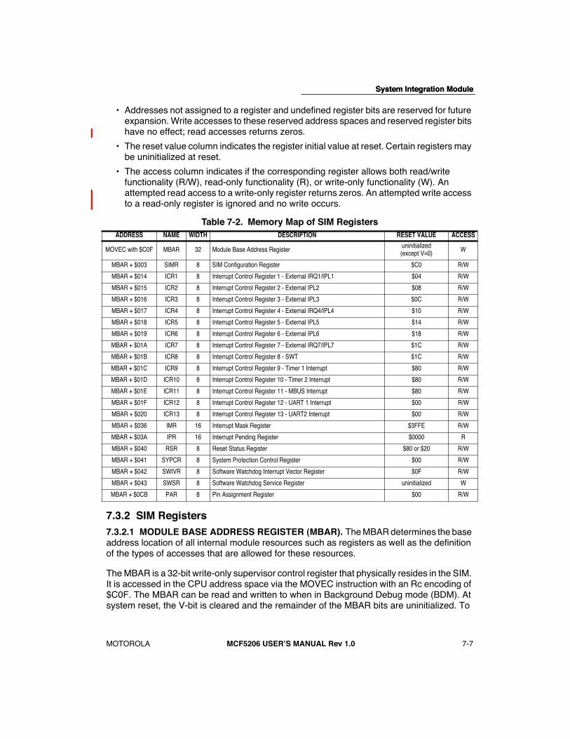
System Integration Module
2
3
4
5
6
7
8
9
10
11
12
13
14
15
16
1
System Integration Module
MOTOROLA
MCF5206 USERÕS MANUAL Rev 1.0
7-7
2
3
4
5
6
7
8
9
10
11
12
13
14
15
16
1
¥ Addresses not assigned to a register and undefined register bits are reserved for future expansion. Write accesses to these reserved address spaces and reserved register bits have no effect; read accesses returns zeros.
¥ The reset value column indicates the register initial value at reset. Certain registers may be uninitialized at reset.
¥ The access column indicates if the corresponding register allows both read/write functionality (R/W), read-only functionality (R), or write-only functionality (W). An attempted read access to a write-only register returns zeros. An attempted write access to a read-only register is ignored and no write occurs.
7.3.2 SIM Registers
7.3.2.1 MODULE BASE ADDRESS REGISTER (MBAR).
The MBAR determines the base address location of all internal module resources such as registers as well as the definition of the types of accesses that are allowed for these resources.
The MBAR is a 32-bit write-only supervisor control register that physically resides in the SIM. It is accessed in the CPU address space via the MOVEC instruction with an Rc encoding of $C0F. The MBAR can be read and written to when in Background Debug mode (BDM). At system reset, the V-bit is cleared and the remainder of the MBAR bits are uninitialized. To
Table 7-2. Memory Map of SIM Registers
ADDRESS NAME WIDTH DESCRIPTION RESET VALUE ACCESS
MOVEC with $C0F MBAR 32 Module Base Address Register uninitialized(except V=0) W
MBAR + $003 SIMR 8 SIM Configuration Register $C0 R/W
MBAR + $014 ICR1 8 Interrupt Control Register 1 - External IRQ1/IPL1 $04 R/W
MBAR + $015 ICR2 8 Interrupt Control Register 2 - External IPL2 $08 R/W
MBAR + $016 ICR3 8 Interrupt Control Register 3 - External IPL3 $0C R/W
MBAR + $017 ICR4 8 Interrupt Control Register 4 - External IRQ4/IPL4 $10 R/W
MBAR + $018 ICR5 8 Interrupt Control Register 5 - External IPL5 $14 R/W
MBAR + $019 ICR6 8 Interrupt Control Register 6 - External IPL6 $18 R/W
MBAR + $01A ICR7 8 Interrupt Control Register 7 - External IRQ7/IPL7 $1C R/W
MBAR + $01B ICR8 8 Interrupt Control Register 8 - SWT $1C R/W
MBAR + $01C ICR9 8 Interrupt Control Register 9 - Timer 1 Interrupt $80 R/W
MBAR + $01D ICR10 8 Interrupt Control Register 10 - Timer 2 Interrupt $80 R/W
MBAR + $01E ICR11 8 Interrupt Control Register 11 - MBUS Interrupt $80 R/W
MBAR + $01F ICR12 8 Interrupt Control Register 12 - UART 1 Interrupt $00 R/W
MBAR + $020 ICR13 8 Interrupt Control Register 13 - UART2 Interrupt $00 R/W
MBAR + $036 IMR 16 Interrupt Mask Register $3FFE R/W
MBAR + $03A IPR 16 Interrupt Pending Register $0000 R
MBAR + $040 RSR 8 Reset Status Register $80 or $20 R/W
MBAR + $041 SYPCR 8 System Protection Control Register $00 R/W
MBAR + $042 SWIVR 8 Software Watchdog Interrupt Vector Register $0F R/W
MBAR + $043 SWSR 8 Software Watchdog Service Register uninitialized W
MBAR + $0CB PAR 8 Pin Assignment Register $00 R/W
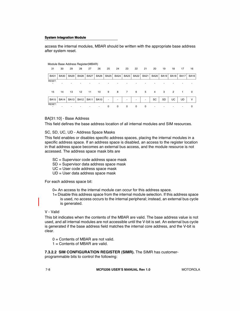
System Integration Module
2
3
4
5
6
7
8
9
10
11
12
13
14
15
16
1
System Integration Module
7-8
MCF5206 USERÕS MANUAL Rev 1.0
MOTOROLA
2
3
4
5
6
7
8
9
10
11
12
13
14
15
16
1
access the internal modules, MBAR should be written with the appropriate base address after system reset.
BA[31:10] - Base AddressThis field defines the base address location of all internal modules and SIM resources.
SC, SD, UC, UD - Address Space MasksThis field enables or disables specific address spaces, placing the internal modules in a specific address space. If an address space is disabled, an access to the register location in that address space becomes an external bus access, and the module resource is not accessed. The address space mask bits are
SC = Supervisor code address space maskSD = Supervisor data address space maskUC = User code address space maskUD = User data address space mask
For each address space bit:
0= An access to the internal module can occur for this address space.1= Disable this address space from the internal module selection. If this address space
is used, no access occurs to the internal peripheral; instead, an external bus cycle is generated.
V - ValidThis bit indicates when the contents of the MBAR are valid. The base address value is not used, and all internal modules are not accessible until the V-bit is set. An external bus cycle is generated if the base address field matches the internal core address, and the V-bit is clear.
0 = Contents of MBAR are not valid.1 = Contents of MBAR are valid.
7.3.2.2 SIM CONFIGURATION REGISTER (SIMR).
The SIMR
has customer- programmable bits to control the following:
BA31 BA30 BA29 BA28 BA27 BA26 BA25 BA24 BA23 BA22 BA21 BA20 BA19 BA18 BA17 BA16
31 30 29 28 27 26 25 24 23 22 21 20 19 18 17 16
- - - - - - - - - - - - - - - -RESET:
BA15 BA14 BA13 BA12 BA11 BA10 - - - - - SC SD UC UD V
15 14 13 12 11 10 9 8 7 6 5 4 3 2 1 0
- - - - - - 0 0 0 0 0 - - - - 0RESET:
Module Base Address Register(MBAR)
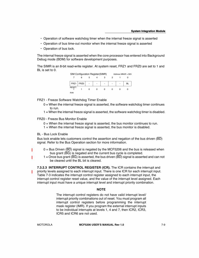
System Integration Module
2
3
4
5
6
7
8
9
10
11
12
13
14
15
16
1
System Integration Module
MOTOROLA
MCF5206 USERÕS MANUAL Rev 1.0
7-9
2
3
4
5
6
7
8
9
10
11
12
13
14
15
16
1
¥ Operation of software watchdog timer when the internal freeze signal is asserted
¥ Operation of bus time-out monitor when the internal freeze signal is asserted
¥ Operation of bus lock.
The internal freeze signal is asserted when the core processor has entered into Background Debug mode (BDM) for software development purposes.
The SIMR is an 8-bit read-write register. At system reset, FRZ1 and FRZ0 are set to 1 and BL is set to 0.
FRZ1 - Freeze Software Watchdog Timer Enable0 = When the internal freeze signal is asserted, the software watchdog timer continues
to run.1 = When the internal freeze signal is asserted, the software watchdog timer is disabled.
FRZ0 - Freeze Bus Monitor Enable0 = When the internal freeze signal is asserted, the bus monitor continues to run.1 = When the internal freeze signal is asserted, the bus monitor is disabled.
BL - Bus Lock EnableBus lock enable lets customers control the assertion and negation of the bus driven (BD) signal. Refer to the Bus Operation section for more information.
0 = Bus Driven (BD) signal is negated by the MCF5206 and the bus is released when bus grant (BG) is negated and the current bus cycle is completed.
1 = Once bus grant (BG) is asserted, the bus driven (BD) signal is asserted and can not be cleared until the BL bit is cleared.
7.3.2.3 INTERRUPT CONTROL REGISTER (ICR).
The ICR contains the interrupt and priority levels assigned to each interrupt input. There is one ICR for each interrupt input. Table 7-3 indicates the interrupt control register assigned to each interrupt input, the interrupt control register reset value, and the value of the interrupt level assigned. Each interrupt input must have a unique interrupt level and interrupt priority combination.
NOTE
The interrupt control registers do not have valid interrupt level/interrupt priority combinations out of reset. You must program allinterrupt control registers before programming the interruptmask register (IMR). If you program the external interrupt inputsto be individual interrupts at levels 1, 4 and 7, then ICR2, ICR3,ICR5 and ICR6 are not used.
FRZ1 FRZ0 - - - - - BL
7 6 5 4 3 2 1 0
1 1 0 0 0 0 0 0RESET:
SIM Configuration Register(SIMR) Address MBAR + $03
R/W

System Integration Module
2
3
4
5
6
7
8
9
10
11
12
13
14
15
16
1
System Integration Module
7-10
MCF5206 USERÕS MANUAL Rev 1.0
MOTOROLA
2
3
4
5
6
7
8
9
10
11
12
13
14
15
16
1
The ICRs are 8-bit read-write registers. See Table 7-3 for the reset values of each ICR.
AVEC - Autovector EnableThis bit determines if the interrupt acknowledge cycle for the interrupt level indicated in IL2-IL0 for each interrupt input requires an autovector response. If this bit is set, a vector number is internally generated, which is the sum of the interrupt level, IL2-IL0, plus 24. Seven distinct autovectors can be used corresponding to the 7 levels of interrupt. If this bit is clear, the external device or internal module must return the vector number during an interrupt acknowledge cycle.
NOTE
For the SWT, the corresponding AVEC is a reserved bit and setto zero, disabling autovector generation in response to SWTgenerated interrupts. The SWT returns the interrupt vector inSWIVR. The AVEC bits in the interrupt control registers for thetimers and MBUS peripherals are reserved and are always setto 1. The autovector value is generated for each of theseinterrupts.
0 = Interrupting source returns vector number during the interrupt-acknowledge cycle.1 = SIM internally generates vector number during the interrupt-acknowledge cycle.
Table 7-3. Interrupt Control Register Assignments
INTERRUPT SOURCEINTERRUPT CONTROL
REGISTER (ICR)ICR RESET VALUE
ICR IINTERRUPT LEVEL(IL2 - IL0) VALUE
External Interrupt Request 1External Interrupt Priority Level 1 ICR1 $04 $1
External Interrupt Priority Level 2 ICR2 $08 $2External Interrupt Priority Level 3 ICR3 $0C $3
External Interrupt Request 4External Interrupt Priority Level 4 ICR4 $10 $4
External Interrupt Priority Level 5 ICR5 $14 $5External Interrupt Priority Level 6 ICR6 $18 $6
External Interrupt Request 7External Interrupt Priority Level 7 ICR7 $1C $7
Software Watchdog Timer ICR8 $1C $7Timer 1 ICR9 $80 User ProgrammableTimer 2 ICR10 $80 User Programmable
MBUS (I
2
C) ICR11 $80 User Programmable
UART 1 ICR12 $00 User ProgrammableUART 2 ICR13 $00 User Programmable
AVEC - - IL2 IL1 IL0 IP1 IP0
7 6 5 4 3 2 1 0
Interrupt Control Register(ICR)
R/W

System Integration Module
2
3
4
5
6
7
8
9
10
11
12
13
14
15
16
1
System Integration Module
MOTOROLA
MCF5206 USERÕS MANUAL Rev 1.0
7-11
2
3
4
5
6
7
8
9
10
11
12
13
14
15
16
1
IL[2:0] - Interrupt LevelThese bits indicate the interrupt level assigned to each interrupt input. Level 7 is the highest priority, level 1 is the lowest, and level 0 indicates that no interrupt is requested. For external interrupts and SWT, the corresponding IL2-IL0 are reserved bits. If the ICRs are programmed to have nonunique interrupt level and priority combination, unpredictable results could occur.
IP[1:0]- Interrupt PriorityThese bits indicate the priority within an interrupt level assigned to each interrupt. You can assign as many as four interrupts to the same interrupt level as long as they have unique interrupt priorities. IP1-IP0 = 3 is the highest priority, and IP1-IP0 = 0 is the lowest priority for a given interrupt level. If you program the ICRs to have nonunique interrupt level and priority combination, unpredictable results could occur.
7.3.2.4 INTERRUPT MASK REGISTER (IMR).
Each bit in the IMR corresponds to an interrupt source. Table 7-4 indicates which mask bit is assigned to each of the interrupt inputs.
You can mask an interrupt by setting the corresponding bit in the IMR and enable an interrupt by clearing the corresponding bit in the IMR. When a masked interrupt occurs, thecorresponding bit in the IPR is still set, regardless of the setting of the IMR bit, but no interrupt request is passed to the core processor.
Table 7-4. Interrupt Mask Register Bit Assignments
INTERRUPT SOURCEINTERRUPT MASK REGISTER
BIT LOCATION
External Interrupt Request 1External Interrupt Priority Level 1 1
External Interrupt Priority Level 2 2External Interrupt Priority Level 3 3
External Interrupt Request 4External Interrupt Priority Level 4 4
External Interrupt Priority Level 5 5External Interrupt Priority Level 6 6
External Interrupt Request 7External Interrupt Priority Level 7 7
Software Watchdog Timer 8Timer 1 9Timer 2 10
MBUS (I
2
C
) 11
UART 1 12UART 2 13
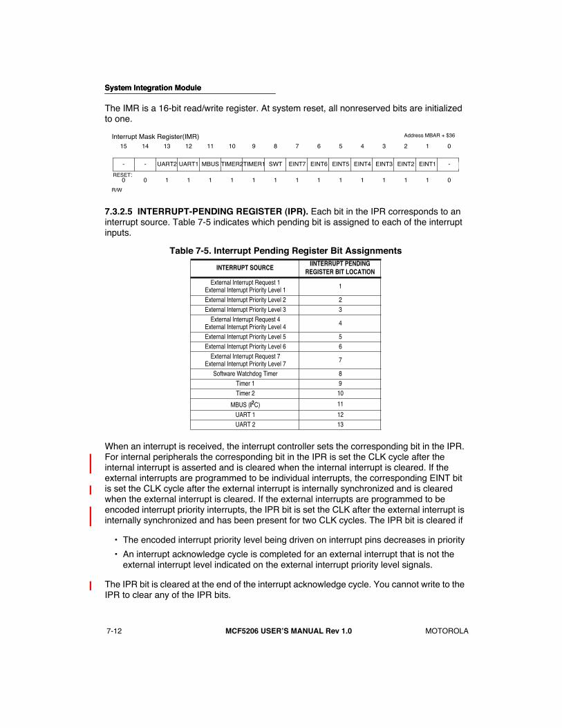
System Integration Module
2
3
4
5
6
7
8
9
10
11
12
13
14
15
16
1
System Integration Module
7-12
MCF5206 USERÕS MANUAL Rev 1.0
MOTOROLA
2
3
4
5
6
7
8
9
10
11
12
13
14
15
16
1
The IMR is a 16-bit read/write register. At system reset, all nonreserved bits are initialized to one.
7.3.2.5 INTERRUPT-PENDING REGISTER (IPR).
Each bit in the IPR corresponds to an interrupt source. Table 7-5 indicates which pending bit is assigned to each of the interrupt inputs.
When an interrupt is received, the interrupt controller sets the corresponding bit in the IPR. For internal peripherals the corresponding bit in the IPR is set the CLK cycle after the internal interrupt is asserted and is cleared when the internal interrupt is cleared. If the external interrupts are programmed to be individual interrupts, the corresponding EINT bit is set the CLK cycle after the external interrupt is internally synchronized and is cleared when the external interrupt is cleared. If the external interrupts are programmed to be encoded interrupt priority interrupts, the IPR bit is set the CLK after the external interrupt is internally synchronized and has been present for two CLK cycles. The IPR bit is cleared if
¥ The encoded interrupt priority level being driven on interrupt pins decreases in priority
¥ An interrupt acknowledge cycle is completed for an external interrupt that is not the external interrupt level indicated on the external interrupt priority level signals.
The IPR bit is cleared at the end of the interrupt acknowledge cycle. You cannot write to the IPR to clear any of the IPR bits.
Table 7-5. Interrupt Pending Register Bit Assignments
INTERRUPT SOURCEIINTERRUPT PENDING
REGISTER BIT LOCATION
External Interrupt Request 1External Interrupt Priority Level 1 1
External Interrupt Priority Level 2 2External Interrupt Priority Level 3 3
External Interrupt Request 4External Interrupt Priority Level 4 4
External Interrupt Priority Level 5 5External Interrupt Priority Level 6 6
External Interrupt Request 7External Interrupt Priority Level 7 7
Software Watchdog Timer 8Timer 1 9Timer 2 10
MBUS (
I
2
C) 11
UART 1 12UART 2 13
- - UART2 UART1 MBUS TIMER2TIMER1 SWT EINT7 EINT6 EINT5 EINT4 EINT3 EINT2 EINT1 -
15 14 13 12 11 10 9 8 7 6 5 4 3 2 1 0
0 0 1 1 1 1 1 1 1 1 1 1 1 1 1 0RESET:
Interrupt Mask Register(IMR) Address MBAR + $36
R/W

System Integration Module
2
3
4
5
6
7
8
9
10
11
12
13
14
15
16
1
System Integration Module
MOTOROLA
MCF5206 USERÕS MANUAL Rev 1.0
7-13
2
3
4
5
6
7
8
9
10
11
12
13
14
15
16
1
An active interrupt request appears as a set bit in the IPR, regardless of the setting of the corresponding mask bit in the IMR.
The IPR is a 16-bit read-only register. At system reset, all bits are initialized to zero.
7.3.2.6 RESET STATUS REGISTER (RSR).
The RSR contains a bit for each reset source to the SIM. A set bit indicates the last type of reset that occurred. The RSR is updated by the reset control logic when the reset is complete. Only one bit is set at any one time in the RSR. You can clear this register by writing a one to that bit location; writing a zero has no effect.
The RSR is an 8-bit read-write register.
HRST - Hard Reset or System Reset1 = The last reset was caused by an external device driving RSTI. Assertion of reset by
an external device causes the core processor to take a reset exception. All registers in internal peripherals and the SIM are reset.
SWTR - Software Watchdog Timer Reset1 = The last reset was caused by the software watchdog timer. If SWRI in the SYPCR
is set and the software watchdog timer times out, a hard reset occurs. RSTO is asserted as an output.
7.3.2.7 SYSTEM PROTECTION CONTROL REGISTER (SYPCR).
The SYPCR controls the software watchdog timer and bus time-out monitor enables and time-out periods.
- - UART2 UART1 MBUS TIMER2TIMER1 SWT EINT7 EINT6 EINT5 EINT4 EINT3 EINT2 EINT1 -
15 14 13 12 11 10 9 8 7 6 5 4 3 2 1 0
0 0 0 0 0 0 0 0 0 0 0 0 0 0 0 0RESET:
Interrupt Pending Register(IPR) Address MBAR + $3a
Read Only
HRST - SWTR - - - - -
7 6 5 4 3 2 1 0
1/0 0 1/0 0 0 0 0 0RESET:
Address MBAR + $40Reset Status Register(RSR)
R/W
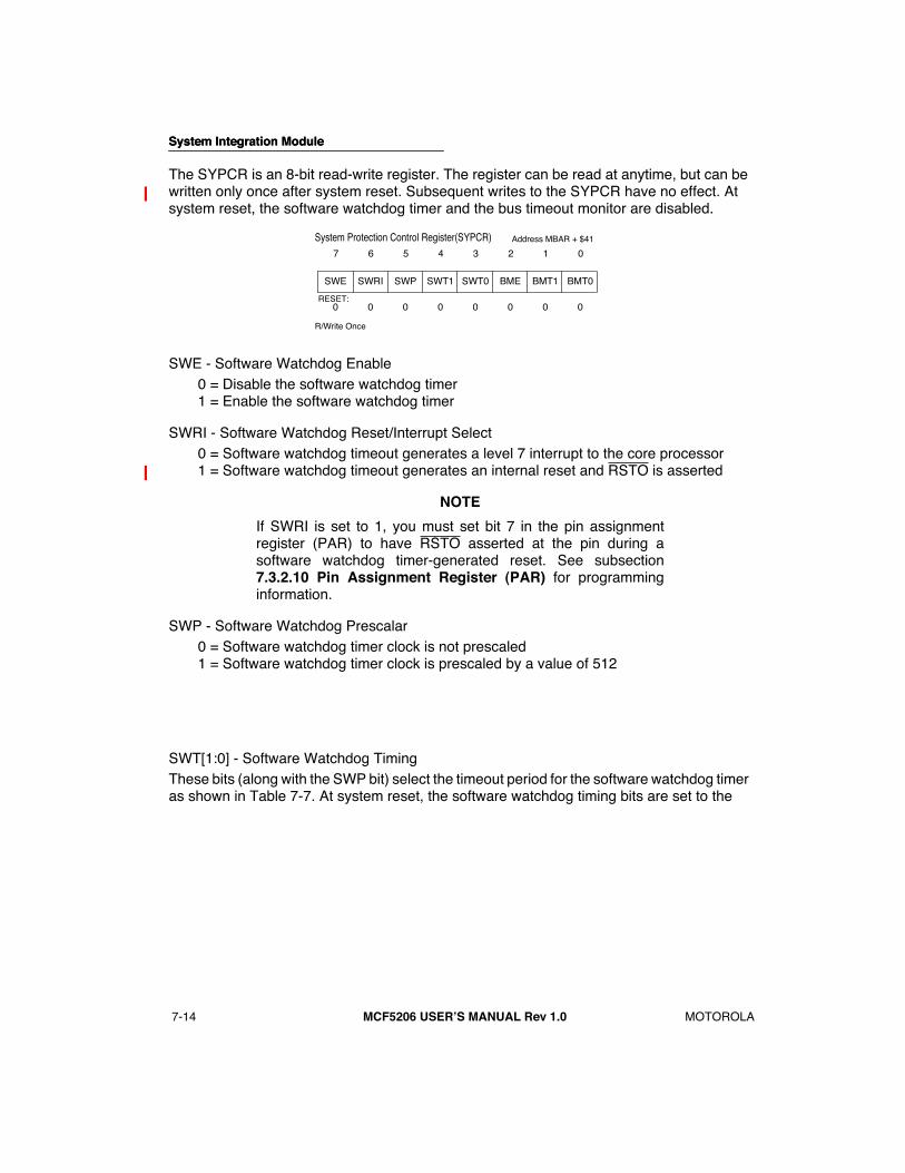
System Integration Module
2
3
4
5
6
7
8
9
10
11
12
13
14
15
16
1
System Integration Module
7-14
MCF5206 USERÕS MANUAL Rev 1.0
MOTOROLA
2
3
4
5
6
7
8
9
10
11
12
13
14
15
16
1
The SYPCR is an 8-bit read-write register. The register can be read at anytime, but can be written only once after system reset. Subsequent writes to the SYPCR have no effect. At system reset, the software watchdog timer and the bus timeout monitor are disabled.
SWE - Software Watchdog Enable0 = Disable the software watchdog timer1 = Enable the software watchdog timer
SWRI - Software Watchdog Reset/Interrupt Select0 = Software watchdog timeout generates a level 7 interrupt to the core processor1 = Software watchdog timeout generates an internal reset and RSTO is asserted
NOTE
If SWRI is set to 1, you must set bit 7 in the pin assignmentregister (PAR) to have RSTO asserted at the pin during asoftware watchdog timer-generated reset. See subsection
7.3.2.10 Pin Assignment Register (PAR)
for programminginformation.
SWP - Software Watchdog Prescalar0 = Software watchdog timer clock is not prescaled1 = Software watchdog timer clock is prescaled by a value of 512
SWT[1:0] - Software Watchdog TimingThese bits (along with the SWP bit) select the timeout period for the software watchdog timer as shown in Table 7-7. At system reset, the software watchdog timing bits are set to the
SWE SWRI SWP SWT1 SWT0 BME BMT1 BMT0
7 6 5 4 3 2 1 0
0 0 0 0 0 0 0 0RESET:
System Protection Control Register(SYPCR) Address MBAR + $41
R/Write Once
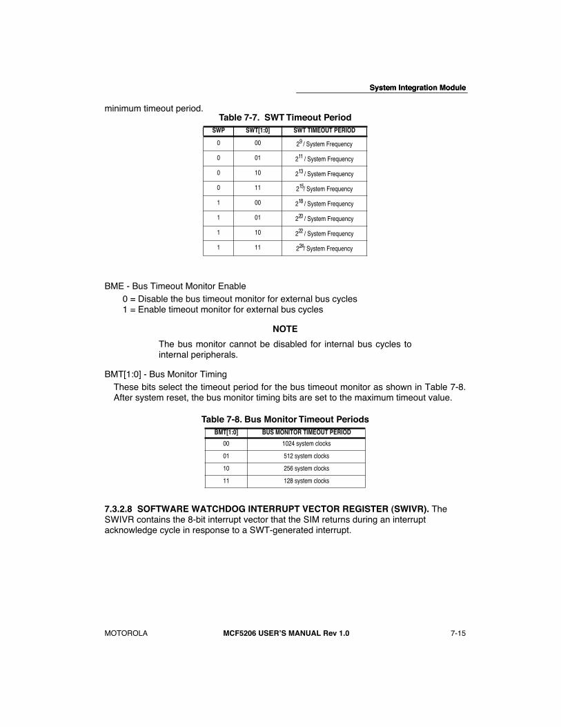
System Integration Module
2
3
4
5
6
7
8
9
10
11
12
13
14
15
16
1System Integration Module
MOTOROLA MCF5206 USERÕS MANUAL Rev 1.0 7-15
2
3
4
5
6
7
8
9
10
11
12
13
14
15
16
1minimum timeout period.
BME - Bus Timeout Monitor Enable0 = Disable the bus timeout monitor for external bus cycles1 = Enable timeout monitor for external bus cycles
NOTE
The bus monitor cannot be disabled for internal bus cycles tointernal peripherals.
BMT[1:0] - Bus Monitor TimingThese bits select the timeout period for the bus timeout monitor as shown in Table 7-8.After system reset, the bus monitor timing bits are set to the maximum timeout value.
7.3.2.8 SOFTWARE WATCHDOG INTERRUPT VECTOR REGISTER (SWIVR). The SWIVR contains the 8-bit interrupt vector that the SIM returns during an interrupt acknowledge cycle in response to a SWT-generated interrupt.
Table 7-7. SWT Timeout PeriodSWP SWT[1:0] SWT TIMEOUT PERIOD
0 00 29 / System Frequency
0 01 211 / System Frequency
0 10 213 / System Frequency
0 11 215/ System Frequency
1 00 218 / System Frequency
1 01 220 / System Frequency
1 10 222 / System Frequency
1 11 224/ System Frequency
Table 7-8. Bus Monitor Timeout PeriodsBMT[1:0] BUS MONITOR TIMEOUT PERIOD
00 1024 system clocks
01 512 system clocks
10 256 system clocks
11 128 system clocks
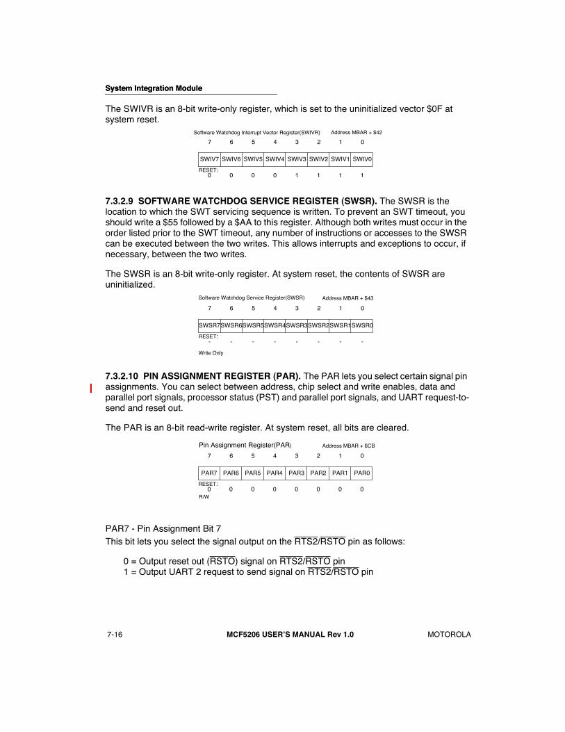
System Integration Module
2
3
4
5
6
7
8
9
10
11
12
13
14
15
16
1System Integration Module
7-16 MCF5206 USERÕS MANUAL Rev 1.0 MOTOROLA
2
3
4
5
6
7
8
9
10
11
12
13
14
15
16
1The SWIVR is an 8-bit write-only register, which is set to the uninitialized vector $0F at system reset.
7.3.2.9 SOFTWARE WATCHDOG SERVICE REGISTER (SWSR). The SWSR is the location to which the SWT servicing sequence is written. To prevent an SWT timeout, you should write a $55 followed by a $AA to this register. Although both writes must occur in the order listed prior to the SWT timeout, any number of instructions or accesses to the SWSR can be executed between the two writes. This allows interrupts and exceptions to occur, if necessary, between the two writes.
The SWSR is an 8-bit write-only register. At system reset, the contents of SWSR are uninitialized.
7.3.2.10 PIN ASSIGNMENT REGISTER (PAR). The PAR lets you select certain signal pin assignments. You can select between address, chip select and write enables, data and parallel port signals, processor status (PST) and parallel port signals, and UART request-to-send and reset out.
The PAR is an 8-bit read-write register. At system reset, all bits are cleared.
PAR7 - Pin Assignment Bit 7This bit lets you select the signal output on the RTS2/RSTO pin as follows:
0 = Output reset out (RSTO) signal on RTS2/RSTO pin1 = Output UART 2 request to send signal on RTS2/RSTO pin
SWIV7 SWIV6 SWIV5 SWIV4 SWIV3 SWIV2 SWIV1 SWIV0
7 6 5 4 3 2 1 0
0 0 0 0 1 1 1 1RESET:
Address MBAR + $42Software Watchdog Interrupt Vector Register(SWIVR)
SWSR7SWSR6SWSR5SWSR4SWSR3SWSR2SWSR1SWSR0
7 6 5 4 3 2 1 0
- - - - - - - -RESET:
Software Watchdog Service Register(SWSR) Address MBAR + $43
Write Only
PAR7 PAR6 PAR5 PAR4 PAR3 PAR2 PAR1 PAR0
7 6 5 4 3 2 1 0
0 0 0 0 0 0 0 0RESET:
Pin Assignment Register(PAR) Address MBAR + $CB
R/W
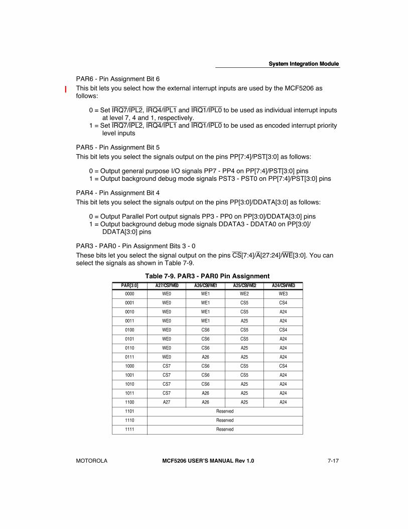
System Integration Module
2
3
4
5
6
7
8
9
10
11
12
13
14
15
16
1System Integration Module
MOTOROLA MCF5206 USERÕS MANUAL Rev 1.0 7-17
2
3
4
5
6
7
8
9
10
11
12
13
14
15
16
1PAR6 - Pin Assignment Bit 6This bit lets you select how the external interrupt inputs are used by the MCF5206 as follows:
0 = Set IRQ7/IPL2, IRQ4/IPL1 and IRQ1/IPL0 to be used as individual interrupt inputs at level 7, 4 and 1, respectively.
1 = Set IRQ7/IPL2, IRQ4/IPL1 and IRQ1/IPL0 to be used as encoded interrupt priority level inputs
PAR5 - Pin Assignment Bit 5This bit lets you select the signals output on the pins PP[7:4]/PST[3:0] as follows:
0 = Output general purpose I/O signals PP7 - PP4 on PP[7:4]/PST[3:0] pins1 = Output background debug mode signals PST3 - PST0 on PP[7:4]/PST[3:0] pins
PAR4 - Pin Assignment Bit 4This bit lets you select the signals output on the pins PP[3:0]/DDATA[3:0] as follows:
0 = Output Parallel Port output signals PP3 - PP0 on PP[3:0]/DDATA[3:0] pins1 = Output background debug mode signals DDATA3 - DDATA0 on PP[3:0]/
DDATA[3:0] pins
PAR3 - PAR0 - Pin Assignment Bits 3 - 0These bits let you select the signal output on the pins CS[7:4]/A[27:24]/WE[3:0]. You can select the signals as shown in Table 7-9.
Table 7-9. PAR3 - PAR0 Pin Assignment PAR[3:0] A27/CS7/WE0 A26/CS6/WE1 A25/CS5/WE2 A24/CS4/WE3
0000 WE0 WE1 WE2 WE3
0001 WE0 WE1 CS5 CS4
0010 WE0 WE1 CS5 A24
0011 WE0 WE1 A25 A24
0100 WE0 CS6 CS5 CS4
0101 WE0 CS6 CS5 A24
0110 WE0 CS6 A25 A24
0111 WE0 A26 A25 A24
1000 CS7 CS6 CS5 CS4
1001 CS7 CS6 CS5 A24
1010 CS7 CS6 A25 A24
1011 CS7 A26 A25 A24
1100 A27 A26 A25 A24
1101 Reserved
1110 Reserved
1111 Reserved
MOTOROLA
MCF5206 USERÕS MANUAL Rev 1.0
8-1
SECTION 8CHIP SELECT MODULE
8.1 INTRODUCTION
The Chip Select module provides user-programmable control of the eight chip select and four write-enable outputs. This subsection describes the operation and programming model of the chip select registers, including the chip select address, mask, and control registers.
8.1.1 Features
The following list summarizes the key chip select features:
¥ Eight programmable chip select signals
¥ Address masking for memory block sizes from 64k to 2G
¥ Programmable wait states and port sizes
¥ Programmable address setup
¥ Programmable address hold for read and write
¥ Programmable wait states and port sizes for default memory
¥ Alternate master access to chip-selects
8.2 CHIP SELECT MODULE I/O
8.2.1 Control Signals
The chip select controller outputs eight chip select and four write-enable signals. The chip select controller activates these signals for ColdFire core-initiated transfers as well as during alternate master-initiated transfers. The chip select controller can also output transfer acknowledge during alternate master transfers.
8.2.1.1 CHIP SELECT (CS[7:0]).
These active-low output signals provide control for peripherals and memory. CS[7:4] are multiplexed with upper address signals (A[27:24]) and the write-enable (WE[3:0]) signals. CS[0] provides the special function of global chip select to let you relocate boot ROM at any defined address space. CS[1] provides the special function of asserting during CPU space accesses including interrupt acknowledge cycles.
8.2.1.2 WRITE-ENABLE (WE[3:0]).
These active-low output signals provide control for peripherals and memory during write transfers. WE[3:0] are multiplexed with upper address and upper chip select signals.
DATE: 9-2-98
REVISION NO.: 1.1
PAGES AFFECTED: SEE CHANGE BARS

Chip Select Module
8-2
MCF5206 USERÕS MANUAL Rev 1.0
MOTOROLA
During a write transfers, these outputs indicate which bytes within a long-word transfer are being selected and which bytes of the data bus are used for the transfer. WE[0] controls D[31:24], WE[1] controls D[23:16], WE[2] controls D[15:8] and WE[3] controls D[7:0]. These signals provide byte data-select signals that are decoded from the SIZx, A[1:0] signals in addition to the programmed port size and burst capability of the memory being accessed, as shown in Table 8-1.
Table 8-1. Data Bus Byte Write-Enable Signals
TRANSFER SIZE PORT SIZE BURST SIZ1 SIZ0 A1 A0WE[0] WE[1] WE[2] WE[3]
D[31:24] D[23:16] D[15:8] D[7:0]
BYTE
8-BIT 0/1 0 1
0 0 0 1 1 1
0 1 0 1 1 1
1 0 0 1 1 1
1 1 0 1 1 1
16-BIT 0/1 0 1
0 0 0 1 1 1
0 1 1 0 1 1
1 0 0 1 1 1
1 1 1 0 1 1
32-BIT 0/1 0 1
0 0 0 1 1 1
0 1 1 0 1 1
1 0 1 1 0 1
1 1 1 1 1 0
WORD
8-BIT
0 0 1
0 0 0 1 1 1
0 1 0 1 1 1
1 0 0 1 1 1
1 1 0 1 1 1
1 1 0
0 0 0 1 1 1
0 1 0 1 1 1
1 0 0 1 1 1
1 1 0 1 1 1
16-BIT 0/1 1 00 0 0 0 1 1
1 0 0 0 1 1
32-BIT 0/1 1 00 0 0 0 1 1
1 0 1 1 0 0

Chip Select Module
MOTOROLA
MCF5206 USERÕS MANUAL Rev 1.0
8-3
8.2.1.3 ADDRESS BUS.
The address bus includes 24 dedicated address signals,A[23:0], and supports as many as four additional address signals, A[27:24]. The chipselect or default memory address appears only on the pins configured to be addresssignals. The maximum size of a memory bank is limited by the number of address signalsavailable (see Table 8-2).
.
For transfers initiated by the ColdFire core, the MCF5206 outputs the address and increments the lower bits during burst transfers, allowing the address bus to be directly
LONG WORD
8-BIT
0 0 1
0 0 0 1 1 1
0 1 0 1 1 1
1 0 0 1 1 1
1 1 0 1 1 1
1 0 0
0 0 0 1 1 1
0 1 0 1 1 1
1 0 0 1 1 1
1 1 0 1 1 1
16-BIT
0 1 00 0 0 0 1 1
1 0 0 0 1 1
1 0 00 0 0 0 1 1
1 0 0 0 1 1
32-BIT 0/1 0 0 0 0 0 0 0 0
LINE
8-BIT
0 0 1
0 0 0 1 1 1
0 1 0 1 1 1
1 0 0 1 1 1
1 1 0 1 1 1
1 1 1
0 0 0 1 1 1
0 1 0 1 1 1
1 0 0 1 1 1
1 1 0 1 1 1
16-BIT
0 1 00 0 0 0 1 1
1 0 0 0 1 1
1 1 10 0 0 0 1 1
1 0 0 0 1 1
32-BIT0 0 0 0 0 0 0 0 0
1 1 1 0 0 0 0 0 0
Table 8-1. Data Bus Byte Write-Enable Signals (Continued)
TRANSFER SIZE PORT SIZE BURST SIZ1 SIZ0 A1 A0WE[0] WE[1] WE[2] WE[3]
D[31:24] D[23:16] D[15:8] D[7:0]

Chip Select Module
8-4
MCF5206 USERÕS MANUAL Rev 1.0
MOTOROLA
connected to external memory. The MCF5206 does not output the address during alternate master initiated transfers to chip select memory.
8.2.1.4 DATA BUS.
You can configure the chip select and default memory spaces to be 8-, 16-, or 32-bits wide. A 32-bit port must reside on data bus bits D[31:0], a 16-bit port must reside on data bus bits D[31:16], and an 8-bit port must reside on data bus bits D[31:24]. This ensures that the MCF5206 correctly transfers valid data to 8-, 16-, and 32-bit ports. Figure 8-1 illustrates the connection of the data bus to 8-, 16-, and 32-bit ports.
Figure 8-1. MCF5206 Interface to Various Port Sizes
8.2.1.5 TRANSFER ACKNOWLEDGE (TA).
Transfer acknowledge is a bidirectional signal that indicates the current data transfer has been successfully completed. You can program TA to be output after a programmed number of wait states during alternate master-initiated transfers that hit in chip select or default memory address space. TA is an input during ColdFire core-initiated transfers that hit in chip select or default memory address space.
8.3 CHIP SELECT OPERATION
The chip select controller provides a glueless interface to certain types of external memory including PROM and peripherals and external control signals for an easy interface to SRAM, EPROM, EEPROM and peripherals. Each of the eight chip select
Table 8-2. Maximum Memory Bank Sizes
AVAILABLE ADDRESS SIGNALS
MAXIMUM CS BANK SIZE
A[23:0] 16 MbyteA[24:0] 32 MbyteA[25:0] 64 MbyteA[26:0] 128 MbyteA[27:0] 256 Mbyte
EXTERNAL
DATA BUS
BYTE 0
8-BIT PORT
16-BIT PORT
32-BIT PORT
BYTE 1
BYTE 2
BYTE 3
BYTE 0 BYTE 1
BYTE 2 BYTE 3
BYTE 0 BYTE 1 BYTE 2 BYTE 3
D[31:24] D[23:16] D[15:8] D[7:0]
Chip Select Module
MOTOROLA
MCF5206 USERÕS MANUAL Rev 1.0
8-5
outputs has an address register, mask register and control register providing individual16-bit address decode, 16-bit address masking, port size and burst capability indication, wait- state generation, automatic acknowledge generation as well as address setup and address hold features.
Chip-selects 0 and 1 provide special functionality. Chip select 0 is a ÒglobalÓ chip select after reset that provides relocatable boot ROM capability. Chip select 1 can be programmed to assert during CPU space accesses including interrupt acknowledge cycles.
The chip select controller also provides a control register for Òdefault memory,Ó which is all of the memory space that is not defined by a chip select or DRAM bank. The default memory control register lets you program features of the default bus transfer including port size, burst capability, and wait-state generation.
8.3.1 Chip Select Bank Definition
The general-purpose chip-selects are controlled by the Chip select Address Register (CSAR), Chip select Mask Register (CSMR), and the Chip select Control Register(CSCR). There is one CSAR, one CSMR, and one CSCR for each chip select signal generated.
8.3.1.1 BASE ADDRESS AND ADDRESS MASKING.
The transfer address generated by the ColdFire core or by an alternate master is compared to the unmasked bits of the base address programmed for each chip select bank in the Chip Select Address Registers (CSAR0 - CSAR7). The masked address bits are controlled by the value programmed in the BAM field in the Chip Select Mask Registers (CSMR0 - CSMR7).
The masking of address bits defines the address space of the chip select bank. Address bits that are masked are not used in the comparison with the transfer address. The base address field (BA31-BA16) in the CSARs and the base address mask field (BAM31-BAM16) in the CSMRs correspond to transfer address bits 31-16. Clearing all bits in the BAM field makes the address space 64 kbyte. For the address space of a chip select bank to be contiguous, address bits should be masked (BAM bits set to a 1) in ascending order starting with A[16].
NOTE
The MCF5206 compares the address for the current bustransfer with the address and mask bits in the chip selectAddress Registers (CSARs), DRAM Controller AddressRegisters (DCARs), the Chip Select Mask Registers
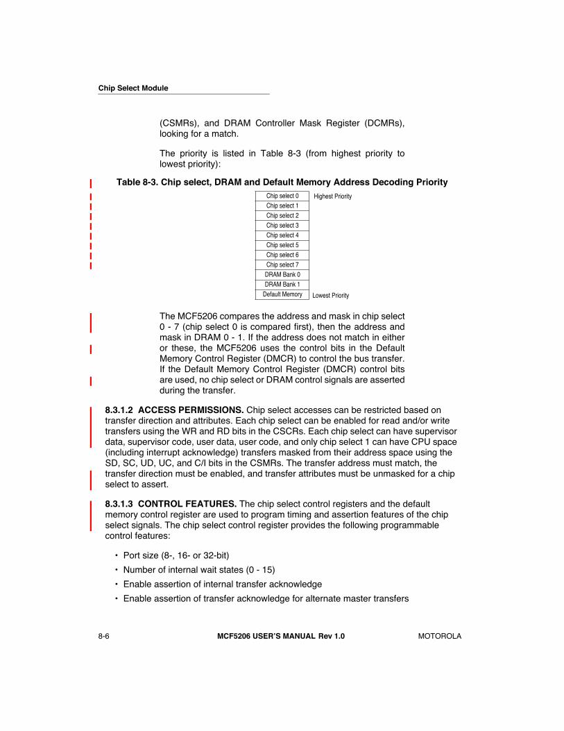
Chip Select Module
8-6
MCF5206 USERÕS MANUAL Rev 1.0
MOTOROLA
(CSMRs), and DRAM Controller Mask Register (DCMRs),looking for a match.
The priority is listed in Table 8-3 (from highest priority tolowest priority):
The MCF5206 compares the address and mask in chip select0 - 7 (chip select 0 is compared first), then the address andmask in DRAM 0 - 1. If the address does not match in eitheror these, the MCF5206 uses the control bits in the DefaultMemory Control Register (DMCR) to control the bus transfer.If the Default Memory Control Register (DMCR) control bitsare used, no chip select or DRAM control signals are assertedduring the transfer.
8.3.1.2 ACCESS PERMISSIONS.
Chip select accesses can be restricted based on transfer direction and attributes. Each chip select can be enabled for read and/or write transfers using the WR and RD bits in the CSCRs. Each chip select can have supervisor data, supervisor code, user data, user code, and only chip select 1 can have CPU space (including interrupt acknowledge) transfers masked from their address space using the SD, SC, UD, UC, and C/I bits in the CSMRs. The transfer address must match, the transfer direction must be enabled, and transfer attributes must be unmasked for a chip select to assert.
8.3.1.3 CONTROL FEATURES.
The chip select control registers and the default memory control register are used to program timing and assertion features of the chip select signals. The chip select control register provides the following programmable control features:
¥ Port size (8-, 16- or 32-bit)
¥ Number of internal wait states (0 - 15)
¥ Enable assertion of internal transfer acknowledge
¥ Enable assertion of transfer acknowledge for alternate master transfers
Table 8-3. Chip select, DRAM and Default Memory Address Decoding Priority
Chip select 0Chip select 1Chip select 2Chip select 3Chip select 4Chip select 5Chip select 6Chip select 7
DRAM Bank 0DRAM Bank 1
Default Memory
Highest Priority
Lowest Priority
Chip Select Module
MOTOROLA
MCF5206 USERÕS MANUAL Rev 1.0
8-7
¥ Enable burst transfers
¥ Address setup
¥ Address hold
¥ Enable read and/or write transfers
8.3.1.3.1 8-, 16-, and 32-Bit Port Sizing.
The general-purpose chip-selects support static bus sizing. You can program the size of the port controlled by a chip select. Defined 8 bit ports are connected to D[31:24]; defined 16-bit ports are connected to D[31:16]; and defined 32 bit ports are connected to D[31:0]. The port size is specified by the PS bits in the CSCR.
8.3.1.3.2 Termination.
The general-purpose chip-selects support three methods of termination: internal termination, synchronous termination, and asynchronous termination. You can program the number of wait states required for each chip select and the default memory individually. You can also enable internal termination for MCF5206- initiated transfers for each chip select and default memory individually.
Transfer acknowledge (TA) can synchronously terminate a transfer. If the MCF5206 initiates a bus transfer and internal termination is enabled (but TA is asserted before the specified number of wait states have been inserted), the transfer terminates on the CLK cycle where TA is asserted.
NOTE
If an alternate master initiates a bus transfer and internaltermination is enabled, TA should not be driven by an externaldevice. The MCF5206 drives TA throughout the alternatemaster access.
Asynchronous transfer acknowledge (ATA) can asynchronously terminate a chip select or default memory transfer. If the MCF5206 initiates a bus transfer and internal termination is enabled but ATA is asserted before the specified number of wait states have been inserted, the transfer terminates on the CLK cycle where the internal asynchronous transfer acknowledge is asserted. If an alternate master initiates a bus transfer and internal termination is enabled, ATA can be driven by an external device to terminate the transfer before the specified number of wait states has been inserted. In this case, the transfer terminates when the internal asynchronous transfer acknowledge is asserted.
8.3.1.3.3 Bursting Control.
The general-purpose chip-selects support burst and non-bursting peripherals and memory. If an external chip select device cannot be accessed using burst transfers, you can program the burst-enable bit in the appropriate Chip Select Control Register (CSCR) or in the Default Memory Control Register (DMCR) to a 0. If the burst-enable bit is set to 1, burst transfers are generated anytime the requested operand size is greater than the programmed chip select or default memory port size. If the burst enable bit is set to 0, nonburst transfers are always generated for the particular chip select
Chip Select Module
8-8
MCF5206 USERÕS MANUAL Rev 1.0
MOTOROLA
or default memory access. Figure 8-5, Figure 8-6, and Figure 8-7 illustrate burst transfers with various settings of address setup, address hold, and 0 wait states.
8.3.1.3.4 Address Setup and Hold Control.
The timing of the assertion and negation of the general-purpose chip-selects and write-enable signals can be programmed on a chip select basis. You can program each chip select to assert when the clock transfer start (TS) is asserted or assert the CLK cycle after transfer start (TS) is asserted. For burst transfers, you can select if the chip select remains valid while the burst address is incremented. You can also program the address, attribute, and data (if the transfer is a write) to remain driven and valid for an additional CLK cycle after the transfer is terminated. Figure 8-2, Figure 8-3, and Figure 8-4 illustrate three transfers with various settings.
8.3.2 Global Chip Select Operation
CS[0] is the global (boot) chip select and as such, allows address decoding for boot ROM before system initialization occurs. Its operation differs from the other external chip select outputs following a system reset. After system reset, CS[0] is asserted for all accesses except for CPU space accesses (including MOVEC transfers and interrupt acknowledge cycles), and internal peripheral accesses. This capability allows the boot ROM to be located at any address in the external address space. CS[0] operates in this manner until CSMR0 is written.
The port size and automatic acknowledge functions of CS[0] are determined by the logic level on pins IRQ1, IRQ4, and IRQ7 sampled on the last rising edge of CLK that RSTI is asserted (see
Bus Operations Section 6.11 Reset Operation
)
.
At system reset, CS[0] allows read and write transfers with address setup, read and write address-hold enabled, and bursting disabled. Writes to CSCR0 does not deactivate the global chip select function; therefore, the number of wait states, read and write enable, address setup, read and write address hold enable, and burst-enable may be changed.
The global chip select functionality is disabled on the first write to CSMR0 after reset. You should set up the appropriate chip select, DRAM, and default memory control registers before writing to CSMR0. Once CSMR0 has been written, the global chip select functionality can be reactivated only by reset.
8.3.3 General Chip Select Operation
The MCF5206 uses the address bus (A[28:0]) to specify the location for a data transfer and the data bus (D[31:0]) to transfer the data. Chip-selects are asserted during bus transfers where the address, transfer direction and type are not masked for the particular chip select. Write-enable signals are asserted on write transfers and indicate the valid byte lanes for the transfer. Write-enable signals are always asserted on the CLK cycle after the chip select is asserted.
Chip select and write enable signals can be asserted during burst and burst inhibited transfers. The assertion and negation timing of the chip select signals are controlled by

Chip Select Module
MOTOROLA
MCF5206 USERÕS MANUAL Rev 1.0
8-9
the address setup, read address hold, and write address hold bits in the chip select control registers.
8.3.3.1 NONBURST TRANSFER WITH NO ADDRESS SETUP AND NO ADDRESS HOLD.
Figure 8-2 illustrates a supervisor data longword write transfer to a 32-bit port. In this case, address setup and write address hold features are disabled.
.
Figure 8-2. Longword Write Transfer from a 32-Bit Port (No Wait State, No Address Setup, No Address Hold)
Clock 1 (C1)
The write cycle starts in C1. During C1, the MCF5206 places valid values on the address bus (A[27:0]) and transfer control signals. The transfer type (TT[1:0]) signals identify the specific access type and access type and mode (ATM) is driven low to identify the transfer as data. The read/write (R/W) signal is driven low for a write cycle, and the size signals (SIZ[1:0]) are driven low to indicate a longword transfer. The MCF5206 asserts transfer
TS
A[27:0]
R/W
CLK
TT[1:0]
ATM
TA
D[31:0]
TEA
SIZ[1:0]
C1 C2
$0
$0
$ADDR
ATA
CS
WE[3:0]

Chip Select Module
8-10
MCF5206 USERÕS MANUAL Rev 1.0
MOTOROLA
start (TS) to indicate the beginning of a bus cycle and asserts the appropriate chip select (CS) for the address being accessed.
Clock 2 (C2)
During C2, the MCF5206 negates transfer start (TS), drives access type and mode (ATM) high to identify the transfer as supervisor and drives data onto D[31:0]. If the selected device(s) is ready to latch the data, it latches D[31:0] and asserts the transfer acknowledge (TA). At the end of C2, the MCF5206 samples the level of TA. If TA is asserted, the transfer of the longword is complete, and the MCF5206 negates CS and WE[3:0] after the next rising edge of CLK. If TA is negated, the MCF5206 continues to sample TA and inserts wait states instead of terminating the transfer. The MCF5206 continues to sample TA on successive rising edge of CLK until it is asserted. If the bus monitor timer is enabled and TA is not asserted before the programmed bus monitor time is reached, the cycle is terminated with an internal bus error.
8.3.3.2 NONBURST TRANSFER WITH ADDRESS SETUP.
Figure 8-3 illustrates a word user data write transfer to a 16-bit port with address setup enabled.
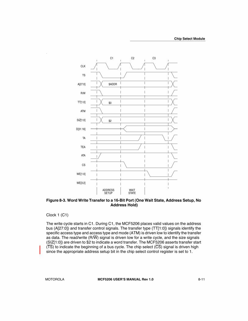
Chip Select Module
MOTOROLA
MCF5206 USERÕS MANUAL Rev 1.0
8-11
.
Figure 8-3. Word Write Transfer to a 16-Bit Port (One Wait State, Address Setup, No Address Hold)
Clock 1 (C1)
The write cycle starts in C1. During C1, the MCF5206 places valid values on the address bus (A[27:0]) and transfer control signals. The transfer type (TT[1:0]) signals identify the specific access type and access type and mode (ATM) is driven low to identify the transfer as data. The read/write (R/W) signal is driven low for a write cycle, and the size signals (SIZ[1:0]) are driven to $2 to indicate a word transfer. The MCF5206 asserts transfer start (TS) to indicate the beginning of a bus cycle. The chip select (CS) signal is driven high since the appropriate address setup bit in the chip select control register is set to 1.
TS
A[27:0]
R/W
CLK
TT[1:0]
ATM
TA
D[31:16]
TEA
SIZ[1:0]
C1 C2
$2
$0
$ADDR
ATA
CS
WE[1:0]
C3
ADDRESSSETUP
WE[3:2]
WAITSTATE

Chip Select Module
8-12
MCF5206 USERÕS MANUAL Rev 1.0
MOTOROLA
Clock 2 (C2)
During C2, the MCF5206 negates transfer start (TS), drives access type and mode (ATM) low to identify the transfer as user and drives data onto D[31:16] and asserts the appropriate chip select (CS) signal. At the end of C2, the MCF5206 samples the level of TA. If TA was asserted the transfer of the word would be complete. Since TA is negated, the MCF5206 continues to output the data and inserts a wait state instead of terminating the transfer.
Clock 3 (C3)
The MCF5206 asserts the write enable (WE[1:0]) signals. If the selected device(s) is ready to latch the data, it latches D[31:0] and asserts the transfer acknowledge (TA). At the end of C3, the MCF5206 samples the level of TA . If TA is asserted, the transfer of the word is complete, and the MCF5206 negates CS and WE[1:0] after the rising edge of CLK. If TA is negated, the MCF5206 continues to sample TA and inserts wait states instead of terminating the transfer. The MCF5206 continues to sample TA on successive rising edge of CLK until it is asserted. If the bus monitor timer is enabled and TA is not asserted before the programmed bus monitor time is reached, the cycle is terminated with an internal bus error.
NOTE
When address setup is enabled (ASET=1), write-enables(WE[3:0]) does not assert on zero wait state write transfers.
8.3.3.3 NONBURST TRANSFER WITH ADDRESS SETUP AND HOLD.
Figure 8-4 illustrates a supervisor data byte write transfer to an 8-bit port with address setup and write address hold enabled.

Chip Select Module
MOTOROLA
MCF5206 USERÕS MANUAL Rev 1.0
8-13
.
Figure 8-4. Byte Write Transfer from an 8-Bit Port (One Wait State, Address Setup, Address Hold)
Clock 1 (C1)
The write cycle starts in C1. During C1, the MCF5206 places valid values on the address bus (A[27:0]) and transfer control signals. The transfer type (TT[1:0]) signals identify the specific access type and access type and mode (ATM) is driven low to identify the transfer as data. The read/write (R/W) signal is driven low for a write cycle, and the size signals (SIZ[1:0]) are driven to $1 to indicate a byte transfer. The MCF5206 asserts transfer start (TS) to indicate the beginning of a bus cycle. The chip select (CS) signal is driven high since the appropriate address setup bit in the chip select control register is set to 1.
Clock 2 (C2)
TS
A[27:0]
R/W
CLK
TT[1:0]
ATM
TA
D[31:16]
TEA
SIZ[1:0]
C1 C2
$1
$0
$ADDR
ATA
CS
WE[0]
C3 C4
WE[3:1]
ADDRESSSETUP
ADDRESSHOLD
WAITSTATE
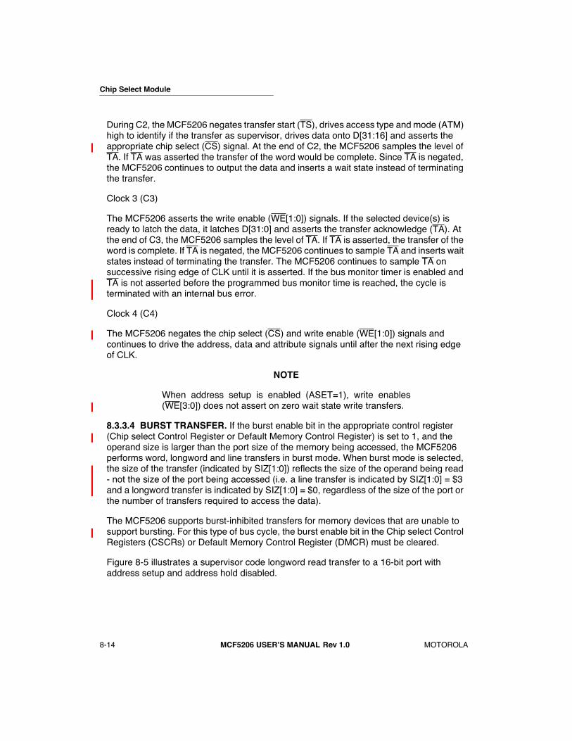
Chip Select Module
8-14
MCF5206 USERÕS MANUAL Rev 1.0
MOTOROLA
During C2, the MCF5206 negates transfer start (TS), drives access type and mode (ATM) high to identify if the transfer as supervisor, drives data onto D[31:16] and asserts the appropriate chip select (CS) signal. At the end of C2, the MCF5206 samples the level of TA. If TA was asserted the transfer of the word would be complete. Since TA is negated, the MCF5206 continues to output the data and inserts a wait state instead of terminating the transfer.
Clock 3 (C3)
The MCF5206 asserts the write enable (WE[1:0]) signals. If the selected device(s) is ready to latch the data, it latches D[31:0] and asserts the transfer acknowledge (TA). At the end of C3, the MCF5206 samples the level of TA. If TA is asserted, the transfer of the word is complete. If TA is negated, the MCF5206 continues to sample TA and inserts wait states instead of terminating the transfer. The MCF5206 continues to sample TA on successive rising edge of CLK until it is asserted. If the bus monitor timer is enabled and TA is not asserted before the programmed bus monitor time is reached, the cycle is terminated with an internal bus error.
Clock 4 (C4)
The MCF5206 negates the chip select (CS) and write enable (WE[1:0]) signals and continues to drive the address, data and attribute signals until after the next rising edge of CLK.
NOTE
When address setup is enabled (ASET=1), write enables(WE[3:0]) does not assert on zero wait state write transfers.
8.3.3.4 BURST TRANSFER.
If the burst enable bit in the appropriate control register (Chip select Control Register or Default Memory Control Register) is set to 1, and the operand size is larger than the port size of the memory being accessed, the MCF5206 performs word, longword and line transfers in burst mode. When burst mode is selected, the size of the transfer (indicated by SIZ[1:0]) reflects the size of the operand being read - not the size of the port being accessed (i.e. a line transfer is indicated by SIZ[1:0] = $3 and a longword transfer is indicated by SIZ[1:0] = $0, regardless of the size of the port or the number of transfers required to access the data).
The MCF5206 supports burst-inhibited transfers for memory devices that are unable to support bursting. For this type of bus cycle, the burst enable bit in the Chip select Control Registers (CSCRs) or Default Memory Control Register (DMCR) must be cleared.
Figure 8-5 illustrates a supervisor code longword read transfer to a 16-bit port with address setup and address hold disabled.
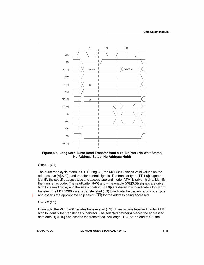
Chip Select Module
MOTOROLA
MCF5206 USERÕS MANUAL Rev 1.0
8-15
.
Figure 8-5. Longword Burst Read Transfer from a 16-Bit Port (No Wait States, No Address Setup, No Address Hold)
Clock 1 (C1)
The burst read cycle starts in C1. During C1, the MCF5206 places valid values on the address bus (A[27:0]) and transfer control signals. The transfer type (TT[1:0]) signals identify the specific access type and access type and mode (ATM) is driven high to identify the transfer as code. The read/write (R/W) and write enable (WE[3:0]) signals are driven high for a read cycle, and the size signals (SIZ[1:0]) are driven low to indicate a longword transfer. The MCF5206 asserts transfer start (TS) to indicate the beginning of a bus cycle and asserts the appropriate chip select (CS) for the address being accessed.
Clock 2 (C2)
During C2, the MCF5206 negates transfer start (TS), drives access type and mode (ATM) high to identify the transfer as supervisor. The selected device(s) places the addressed data onto D[31:16] and asserts the transfer acknowledge (TA). At the end of C2, the
TS
A[27:0]
R/W
CLK
TT[1:0]
ATM
TA
D[31:16]
TEA
SIZ[1:0]
C1 C2
$0
$0
$ADDR
ATA
CS
WE[3:0]
C3
$ADDR + 2
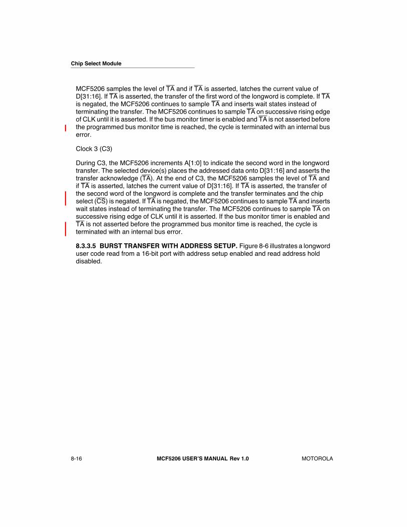
Chip Select Module
8-16
MCF5206 USERÕS MANUAL Rev 1.0
MOTOROLA
MCF5206 samples the level of TA and if TA is asserted, latches the current value of D[31:16]. If TA is asserted, the transfer of the first word of the longword is complete. If TA is negated, the MCF5206 continues to sample TA and inserts wait states instead of terminating the transfer. The MCF5206 continues to sample TA on successive rising edge of CLK until it is asserted. If the bus monitor timer is enabled and TA is not asserted before the programmed bus monitor time is reached, the cycle is terminated with an internal bus error.
Clock 3 (C3)
During C3, the MCF5206 increments A[1:0] to indicate the second word in the longword transfer. The selected device(s) places the addressed data onto D[31:16] and asserts the transfer acknowledge (TA). At the end of C3, the MCF5206 samples the level of TA and if TA is asserted, latches the current value of D[31:16]. If TA is asserted, the transfer of the second word of the longword is complete and the transfer terminates and the chip select (CS) is negated. If TA is negated, the MCF5206 continues to sample TA and inserts wait states instead of terminating the transfer. The MCF5206 continues to sample TA on successive rising edge of CLK until it is asserted. If the bus monitor timer is enabled and TA is not asserted before the programmed bus monitor time is reached, the cycle is terminated with an internal bus error.
8.3.3.5 BURST TRANSFER WITH ADDRESS SETUP.
Figure 8-6 illustrates a longword user code read from a 16-bit port with address setup enabled and read address hold disabled.
Chip Select Module
MOTOROLA
MCF5206 USERÕS MANUAL Rev 1.0
8-17
.
Figure 8-6. Longword Burst Read Transfer from a 16-Bit Port (No Wait States, Address Setup, No Address Hold)
Clock 1 (C1)
The burst read cycle starts in C1. During C1, the MCF5206 places valid values on the address bus (A[27:0]) and transfer control signals. The transfer type (TT[1:0]) signals identify the specific access type and access type and mode (ATM) is driven high to identify the transfer as reading code. The read/write (R/W) and write enable (WE[3:0]) signals are driven high for a read cycle, and the size signals (SIZ[1:0]) are driven low to indicate a longword transfer. The MCF5206 asserts transfer start (TS) to indicate the beginning of a bus cycle. The chip select (CS) signal is driven high since the appropriate address setup bit in the chip select control register is set to 1.
TS
A[27:0]
R/W
CLK
TT[1:0]
ATM
TA
D[31:16]
TEA
SIZ[1:0]
C1 C2
$0
$0
$ADDR
ATA
CS
WE[3:0]
C3 C4
$ADDR + 2
ADDRESSSETUP
ADDRESSSETUP
Chip Select Module
8-18
MCF5206 USERÕS MANUAL Rev 1.0
MOTOROLA
Clock 2 (C2)
During C2, the MCF5206 negates transfer start (TS), drives access type and mode (ATM) low to identify if the transfer as user. The appropriate chip select (CS) signal is asserted. The selected device(s) places the addressed data onto D[31:16] and asserts the transfer acknowledge (TA). At the end of C2, the MCF5206 samples the level of TA and if TA is asserted, latches the current value of D[31:16]. If TA is asserted, the transfer of the first word of the longword is complete and chip select (CS) is negated after the next rising edge of CLK. If TA is negated, the MCF5206 continues to sample TA and inserts wait states instead of terminating the transfer. The MCF5206 continues to sample TA on successive rising edge of CLK until it is asserted. If the bus monitor timer is enabled and TA is not asserted before the programmed bus monitor time is reached, the cycle is terminated with an internal bus error.
Clock 3 (C3)
During C3, the MCF5206 increments A[1:0] to indicate the second word in the longword transfer. The chip select (CS) signal is driven high since the appropriate address setup bit in the chip select control register is set to 1.
Clock 4 (C4)
The selected device(s) places the addressed data onto D[31:16] and asserts the transfer acknowledge (TA). At the end of C4, the MCF5206 samples the level of TA and if TA is asserted, latches the current value of D[31:16]. If TA is asserted, the transfer of the second word of the longword is complete and the transfer terminates and the chip select (CS) is negated. If TA is negated, the MCF5206 continues to sample TA and inserts wait states instead of terminating the transfer. The MCF5206 continues to sample TA on successive rising edge of CLK until it is asserted. If the bus monitor timer is enabled and TA is not asserted before the programmed bus monitor time is reached, the cycle is terminated with an internal bus error.
NOTE
When address setup is enabled (ASET=1), write enables(WE[3:0]) does not assert on zero wait state write transfers.
8.3.3.6 BURST TRANSFER WITH ADDRESS SETUP AND HOLD.
Figure 8-7 illustrates a supervisor data word read transfer from an 8-bit port with address setup and read address hold enabled.

Chip Select Module
MOTOROLA
MCF5206 USERÕS MANUAL Rev 1.0
8-19
.
Figure 8-7. Word Burst Read Transfer from an 8-Bit Port (No Wait States, Address Setup, Address Hold)
Clock 1 (C1)
The burst read cycle starts in C1. During C1, the MCF5206 places valid values on the address bus (A[27:0]) and transfer control signals. The transfer type (TT[1:0]) signals identify the specific access type and access type and mode (ATM) is driven low to identify the transfer as reading data. The read/write (R/W) and write enable (WE[3:0]) signals are driven high for a read cycle, and the size signals (SIZ[1:0]) are driven to $2 to indicate a word transfer. The MCF5206 asserts transfer start (TS) to indicate the beginning of a bus cycle. The chip select (CS) signal is driven high since the appropriate address setup bit in the chip select control register is set to 1.
TS
A[27:0]
R/W
CLK
TT[1:0]
ATM
TA
D[31:24]
TEA
SIZ[1:0]
C1 C2
$2
$0
$ADDR
ATA
CS
WE[3:0]
C3 C4
$ADDR + 1
C5 C6
ADDRESSSETUP
ADDRESSHOLD
Chip Select Module
8-20
MCF5206 USERÕS MANUAL Rev 1.0
MOTOROLA
Clock 2 (C2)
During C2, the MCF5206 negates transfer start (TS), drives access type and mode (ATM) high to identify the transfer as supervisor. The appropriate chip select (CS) signal is asserted. The selected device(s) places the addressed data onto D[31:24] and asserts the transfer acknowledge (TA). At the end of C2, the MCF5206 samples the level of TA and if TA is asserted, latches the current value of D[31:24]. If TA is asserted, the transfer of the first byte of the word is complete and chip select (CS) is negated after the next rising edge of CLK. If TA is negated, the MCF5206 continues to sample TA and inserts wait states instead of terminating the transfer. The MCF5206 continues to sample TA on successive rising edge of CLK until it is asserted. If the bus monitor timer is enabled and TA is not asserted before the programmed bus monitor time is reached, the cycle is terminated with an internal bus error.
Clock 3 (C3)
The MCF5206 continues to drive address and bus attributes since the read address hold bit in the appropriate chip select control register is set to 1.
Clock 4(C4)
During C3, the MCF5206 increments A[0] to indicate the second byte in the word transfer. The chip select (CS) signal is driven high since the appropriate address setup bit in the chip select control register is set to 1.
Clock 5(C5)
The selected device(s) places the addressed data onto D[31:24] and asserts the transfer acknowledge (TA). At the end of C5, the MCF5206 samples the level of TA and if TA is asserted, latches the current value of D[31:24]. If TA is asserted, the transfer of the second word of the longword is complete and the transfer terminates and the chip select (CS) is negated. If TA is negated, the MCF5206 continues to sample TA and inserts wait states instead of terminating the transfer. The MCF5206 continues to sample TA on successive rising edge of CLK until it is asserted. If the bus monitor timer is enabled and TA is not asserted before the programmed bus monitor time is reached, the cycle is terminated with an internal bus error.
Clock 6 (C6)
The MCF5206 continues to drive address and bus attributes since the read address hold bit in the appropriate chip select control register is set to 1.
NOTE
When address setup is enabled (ASET=1), write enables(WE[3:0]) does not assert on zero wait state write transfers.

Chip Select Module
MOTOROLA
MCF5206 USERÕS MANUAL Rev 1.0
8-21
8.3.4 Alternate Master Chip Select Operation
The MCF5206 can monitor bus transfers by other bus masters and assert chip select and transfer termination signals during these transfers. Assertion of chip select and termination signals occurs when the bus is granted to another bus master and TS is asserted by the alternate master as an input to the MCF5206. The MCF5206 registers the value of A[27:0], R/W and SIZ[1:0] on the rising edge of CLK in which TS is asserted.
NOTE
If the pins A[27:24]/CS[7:4]/WE[0:3] are not assigned tooutput address signals, a value of $0 is assigned internally tothese signals. Also, TT[1:0] and ATM are not examined duringalternate master transfers. The mask bits: SC, SD, UC, UD,and C/I in the Chip select Mask Registers (CSMR) are notused during alternate master transfers.
The MCF5206 examines the address, direction and size of the transfer and on the next rising edge of CLK, begins assertion of the proper sequence of memory control signals. If the transfer is decoded to be a chip select address and the chip select is enabled for the direction of the transfer (read and/or write enabled), the appropriate chip select and write enable signals are asserted. If the chip select is enabled for alternate master automatic acknowledge, TA is driven and asserted at the appropriate time. The MCF5206 does not drive address during external bus master accesses that are decoded as chip select or default memory transfers. The alternate master must provide the correct address to the external memory at the appropriate time.
If the address of the transfer is neither a chip select or a DRAM address, the SIM reads the Default Memory Control Register (DMCR). If the alternate master automatic acknowledge (EMAA) bit in the DMCR is set, the MCF5206 drives transfer acknowledge (TA) as an output and asserts transfer acknowledge after the number of clocks programmed in the wait state bits (WS) in the DMCR.
8.3.4.1 ALTERNATE MASTER NONBURST TRANSFER.
The general-purpose chip-selects support burst and nonbursting peripherals and memory for alternate master accesses. If an external chip select device can not be accessed using burst transfers, you can program the burst-enable bit in the appropriate Chip Select Control Register (CSCR) or in the DMCR to 0. If the burst-enable bit is set to 1, and the alternate master initiates a transfer where the transfer size is greater than the programmed port size, the MCF5206 asserts the chip select control signals for a burst transfer. If the burst enable bit is set to 0, the alternate master should never initiate a transfer with the size specified as larger than the programmed port size. Figure 8-8 illustrates a longword read transfer initiated by an alternate master to a 32-bit port.

Chip Select Module
8-22
MCF5206 USERÕS MANUAL Rev 1.0
MOTOROLA
.
Figure 8-8. Alternate Master Longword Read Transfer from a 32-Bit Port (No Wait State, No Address Setup, No Address Hold)
Clock 1 (C1)
The write cycle starts in C1. During C1, the alternate master places valid values on the address bus (A[27:0]) and transfer control signals. The MCF5206 registers the alternate master address, read/write and size signals.
Clock 2 (C2)
During C2, the alternate master negates transfer start (TS). The MCF5206 compares the alternate master address to the internal chip select addresses and enables the appropriate chip select for assertion.
Clock 3 (C3)
The MCF5206 asserts the appropriate chip select and since the EMAA bit in the appropriate Chip select Control Register (CSCR) is set to one, asserts transfer acknowledge (TA). The selected device drive data onto D[31:0]. At the end of C3, the alternate master samples the level of TA. If TA is asserted, the transfer of the longword is
TS
A[27:0]
R/W
CLK
TA
D[31:0]
TEA
SIZ[1:0]
C1 C2
$0
$ADDR
ATA
CS
WE[3:0]
C3 C4
Chip Select Module
MOTOROLA
MCF5206 USERÕS MANUAL Rev 1.0
8-23
complete. If TA is negated, the alternate master continues to sample TA and inserts wait states instead of terminating the transfer.
Clock 4 (C4)
At the start of clock 4, the MCF5206 negates CS and TA, completing the alternate master transfer. After the next rising edge of CLK, the MCF5206 three states TA. The alternate master can assert TS starting another transfer.
8.3.4.2 ALTERNATE MASTER BURST TRANSFER.
The timing of the assertion and negation of the general-purpose chip-selects and write-enable signals during alternate master accesses can be programmed on a chip select basis. The address setup and hold features of the chip-selects are not used during nonburst alternate master accesses. The address setup and hold features can insert CLK cycles where the chip select is negated, during burst cycles. During alternate master read transfers, the MCF5206 drives the activated chip select signal negated for one CLK cycle for each of the address setup and read address hold bits that are set to 1. During alternate master write transfers, the MCF5206 drives the activated chip select signal negated for one CLK cycle for each of the address setup and write address hold bits that are set to 1. Figure 8-9 illustrates a bursting longword read transfer from a 16-bit port with no address setup and no address hold.
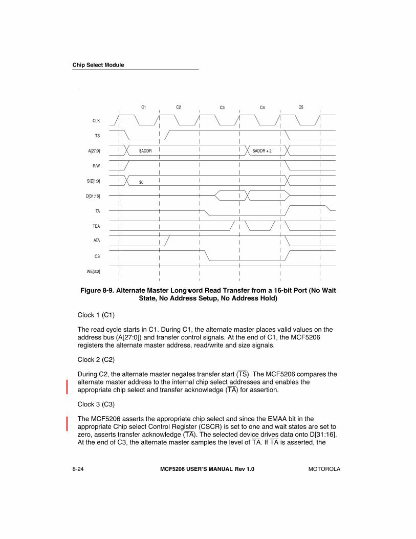
Chip Select Module
8-24
MCF5206 USERÕS MANUAL Rev 1.0
MOTOROLA
.
Figure 8-9. Alternate Master Longword Read Transfer from a 16-bit Port (No Wait State, No Address Setup, No Address Hold)
Clock 1 (C1)
The read cycle starts in C1. During C1, the alternate master places valid values on the address bus (A[27:0]) and transfer control signals. At the end of C1, the MCF5206 registers the alternate master address, read/write and size signals.
Clock 2 (C2)
During C2, the alternate master negates transfer start (TS). The MCF5206 compares the alternate master address to the internal chip select addresses and enables the appropriate chip select and transfer acknowledge (TA) for assertion.
Clock 3 (C3)
The MCF5206 asserts the appropriate chip select and since the EMAA bit in the appropriate Chip select Control Register (CSCR) is set to one and wait states are set to zero, asserts transfer acknowledge (TA). The selected device drives data onto D[31:16]. At the end of C3, the alternate master samples the level of TA. If TA is asserted, the
TS
A[27:0]
R/W
CLK
TA
D[31:16]
TEA
SIZ[1:0]
C1 C2
$0
$ADDR
ATA
CS
WE[3:0]
C3 C4 C5
$ADDR + 2

Chip Select Module
MOTOROLA
MCF5206 USERÕS MANUAL Rev 1.0 8-25
transfer of the first word of the longword is complete. If TA is negated, the alternate master continues to sample TA and inserts wait states instead of terminating the transfer.
Clock 4 (C4)
At the start of clock 4, the alternate master increments the address to indicate the second word of the longword transfer. The MCF5206 continues to assert CS and TA and the selected slave outputs the data indicated by the new address on D[31:16]. At the end of clock 4, the alternate master samples the level of TA. If TA is asserted, the transfer of the second word of the longword is complete. If TA is negated, the alternate master continues to sample TA and inserts wait states instead of terminating the transfer.
Clock 5 (C5)
At the start of clock 5, the MCF5206 negates CS and TA, completing the alternate master transfer. After the next rising edge of CLK, the MCF5206 three states TA. The alternate master can assert TS starting another transfer.
NOTE
Write enables (WE[3:0]) does not assert on zero wait statealternate master write transfers.
8.3.4.3 ALTERNATE MASTER BURST TRANSFER WITH ADDRESS SETUP AND HOLD. Figure 8-10 illustrates a longword bursting read transfer from a 16-bit port with either address setup or read address hold enabled.
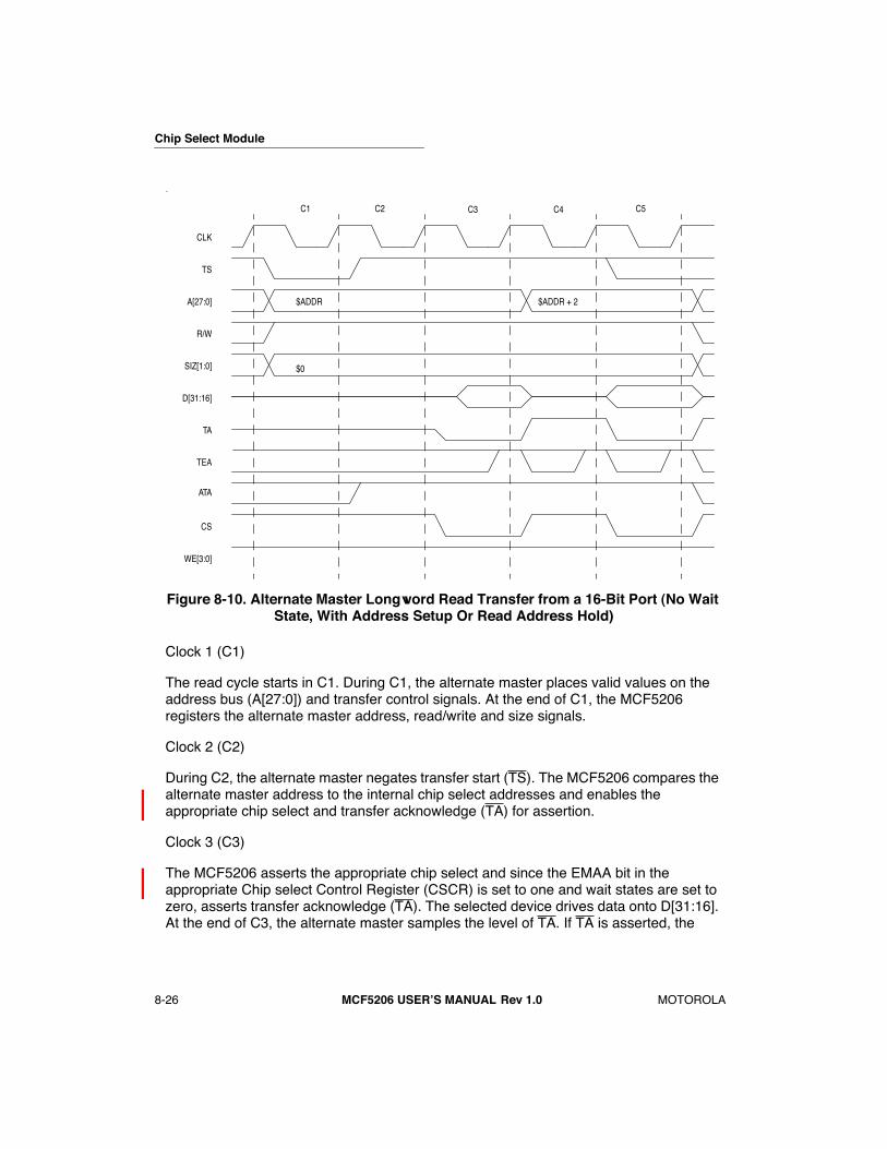
Chip Select Module
8-26 MCF5206 USERÕS MANUAL Rev 1.0 MOTOROLA
.
Figure 8-10. Alternate Master Longword Read Transfer from a 16-Bit Port (No Wait State, With Address Setup Or Read Address Hold)
Clock 1 (C1)
The read cycle starts in C1. During C1, the alternate master places valid values on the address bus (A[27:0]) and transfer control signals. At the end of C1, the MCF5206 registers the alternate master address, read/write and size signals.
Clock 2 (C2)
During C2, the alternate master negates transfer start (TS). The MCF5206 compares the alternate master address to the internal chip select addresses and enables the appropriate chip select and transfer acknowledge (TA) for assertion.
Clock 3 (C3)
The MCF5206 asserts the appropriate chip select and since the EMAA bit in the appropriate Chip select Control Register (CSCR) is set to one and wait states are set to zero, asserts transfer acknowledge (TA). The selected device drives data onto D[31:16]. At the end of C3, the alternate master samples the level of TA. If TA is asserted, the
TS
A[27:0]
R/W
CLK
TA
D[31:16]
TEA
SIZ[1:0]
C1 C2
$0
$ADDR
ATA
CS
WE[3:0]
C3 C4 C5
$ADDR + 2

Chip Select Module
MOTOROLA MCF5206 USERÕS MANUAL Rev 1.0 8-27
transfer of the first word of the longword is complete. If TA is negated, the alternate master continues to sample TA and inserts wait states instead of terminating the transfer.
Clock 4 (C4)
At the start of clock 4, the alternate master increments the address to indicate the second word of the longword transfer. The MCF5206 negates CS and TA.
Clock 5 (C5)
At the start of clock 5, the MCF5206 asserts CS and TA. The selected slave outputs the data indicated by the address on D[31:16]. At the end of clock 4, the alternate master samples the level of TA. If TA is asserted, the transfer of the second word of the longword is complete. If TA is negated, the alternate master continues to sample TA and inserts wait states instead of terminating the transfer.
After the next rising edge of CLK, the MCF5206 negates CS and TA, completing the alternate master transfer. After the next rising edge of CLK, the MCF5206 three states TA. The alternate master can assert TS starting another transfer.
NOTE
Write enables (WE[3:0]) does not assert on zero wait statealternate master write transfers.
8.4 PROGRAMMING MODEL
8.4.1 Chip Select Registers Memory MapTable 8-4 shows the memory map of all the chip select module registers. The internal registers in the chip select module are memory-mapped registers offset from the MBAR address pointer.
The following lists several keynotes regarding the programming model table:
¥ Addresses not assigned to a register and undefined register bits are reserved for future expansion. Write accesses to these reserved address spaces and reserved register bits have no effect; read accesses returns zeros.
¥ The reset value column indicates the register initial value at reset. Certain registers may be uninitialized at reset, i.e., they may contain random values after reset.
Table 8-4. Memory Map of Chip Select Registers
ADDRESS NAME WIDTH DESCRIPTION RESET VALUE ACCESS
MBAR +$ 64 CSAR0 16 Chip Select Address Register - Bank 0 0000 R/W
MBAR +$ 68 CSMR0 32 Chip Select Mask Register - Bank 0 00000000 R/W

Chip Select Module
8-28 MCF5206 USERÕS MANUAL Rev 1.0 MOTOROLA
MBAR + $6E CSCR0 16 Chip Select Control Register - Bank 0
3C1F, 3C5F, 3C9F, 3CDF, 3D1F, 3D5F, 3D9F, or 3DDFAA set by IRQ7 at resetPS1 set by IRQ4 at resetPS0 set by IRQ1 at reset
R/W
MBAR + $70 CSAR1 16 Chip Select Address Register - Bank 1 uninitialized R/W
MBAR + $74 CSMR1 32 Chip Select Mask Register - Bank 1 uninitialized R/W
MBAR + $7A CSCR1 16 Chip Select Control Register - Bank 1uninitialized(except BRST=ASET=WRAH=RDAH=WR=RD=0)
R/W
MBAR + $7C CSAR2 16 Chip Select Address Register - Bank 2 uninitialized R/W
MBAR + $80 CSMR2 32 Chip Select Mask Register - Bank 2 uninitialized R/W
MBAR + $86 CSCR2 16 Chip Select Control Register - Bank 2uninitialized(except BRST=ASET=WRAH=RDAH=WR=RD=0)
R/W
MBAR + $88 CSAR3 16 Chip Select Address Register - Bank 3 uninitialized R/W
MBAR + $8C CSMR3 32 Chip Select Mask Register - Bank 3 uninitialized R/W
MBAR + $92 CSCR3 16 Chip Select Control Register - Bank 3uninitialized(except BRST=ASET=WRAH=RDAH=WR=RD=0)
R/W
MBAR + $94 CSAR4 16 Chip Select Address Register - Bank 4 uninitialized R/W
MBAR +$ 98 CSMR4 32 Chip Select Mask Register - Bank 4 uninitialized R/W
MBAR +$ 9E CSCR4 16 Chip Select Control Register - Bank 4uninitialized(except BRST=ASET=WRAH=RDAH=WR=RD=0)
R/W
MBAR + $A0 CSAR5 16 Chip Select Address Register - Bank 5 uninitialized R/W
MBAR + $A4 CSMR5 32 Chip Select Mask Register - Bank 5 uninitialized R/W
MBAR + $AA CSCR5 16 Chip Select Control Register - Bank 5uninitialized(except BRST=ASET=WRAH=RDAH=WR=RD=0)
R/W
MBAR + $AC CSAR6 16 Chip Select Address Register - Bank 6 uninitialized R/W
MBAR + $B0 CSMR6 32 Chip Select Mask Register - Bank 6 uninitialized R/W
MBAR + $B6 CSCR6 16 Chip Select Control Register - Bank 6uninitialized(except BRST=ASET=WRAH=RDAH=WR=RD=0)
R/W
Table 8-4. Memory Map of Chip Select Registers (Continued)
ADDRESS NAME WIDTH DESCRIPTION RESET VALUE ACCESS

Chip Select Module
MOTOROLA MCF5206 USERÕS MANUAL Rev 1.0 8-29
8.4.2 Chip Select Controller Registers8.4.2.1 CHIP SELECT ADDRESS REGISTER (CSAR0 - CSAR7). Each CSAR determines the base address of the corresponding chip select pin.
Each CSAR is a 16-bit read/write register. CSAR0 is initialized to $0000 at reset and CSAR1-CSAR7 are unaffected (uninitialized) by reset.
.
.
BA31-BA16 - Base AddressThis field defines the base address location of memory dedicated to each chip select. These bits are compared to ColdFire core address bus bits 31-16 to determine if the chip select memory is being accessed. During alternate master accesses these bits are compared as shown in Table 8-5.
MBAR +$ B8 CSAR7 16 Chip Select Address Register - Bank 7 uninitialized R/W
MBAR + $BC CSMR7 32 Chip Select Mask Register - Bank 7 uninitialized R/W
MBAR +$ C2 CSCR7 16 Chip Select Control Register - Bank 7uninitialized(except BRST=ASET=WRAH=RDAH=WR=RD=0)
R/W
MBAR + $C6 DMCR 16 Default Memory Control Register 0000 R/W
Table 8-5. BA Field Comparisons for Alternate Master Transfers
BA BIT COMPARED TO CONDITIONS
BA31 - BA28 $0 Always
BA27$0 A[27]/CS[7]/WE[0] does not output A[27]
A[27] A[27]/CS[7]/WE[0] outputs A[27]
BA26$0 A[26]/CS[6]/WE[1] does not output A[26]
A[26] A[26]/CS[6]/WE[1] outputs A[26]
Table 8-4. Memory Map of Chip Select Registers (Continued)
ADDRESS NAME WIDTH DESCRIPTION RESET VALUE ACCESS
BA31 BA30 BA29 BA28 BA27 BA26 BA25 BA24 BA23 BA22 BA21 BA20 BA19 BA18 BA17 BA16
15 14 13 12 11 10 9 8 7 6 5 4 3 2 1 0
0 0 0 0 0 0 0 0 0 0 0 0 0 0 0 0RESET:
Chip Select Address Register(CSAR0) MBAR + $64
BA31 BA30 BA29 BA28 BA27 BA26 BA25 BA24 BA23 BA22 BA21 BA20 BA19 BA18 BA17 BA16
15 14 13 12 11 10 9 8 7 6 5 4 3 2 1 0
- - - - - - - - - - - - - - - -RESET:
Chip select Address Register (CSAR1 - CSAR7)
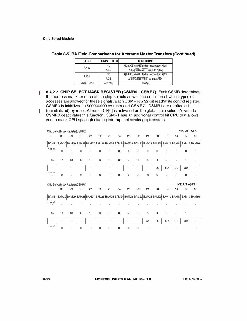
Chip Select Module
8-30 MCF5206 USERÕS MANUAL Rev 1.0 MOTOROLA
8.4.2.2 CHIP SELECT MASK REGISTER (CSMR0 - CSMR7). Each CSMR determines the address mask for each of the chip-selects as well the definition of which types of accesses are allowed for these signals. Each CSMR is a 32-bit read/write control register. CSMR0 is initialized to $00000000 by reset and CSMR7 - CSMR1 are unaffected (uninitialized) by reset. At reset, CS[0] is activated as the global chip select. A write to CSMR0 deactivates this function. CSMR1 has an additional control bit CPU that allows you to mask CPU space (including interrupt acknowledge) transfers.
BA25$0 A[25]/CS[5]/WE[2] does not output A[25]
A[25] A[25]/CS[5]/WE2 outputs A[25]
BA24$0 A[24]/CS[4]/WE[3] does not output A[24]
A[24] A[24]/CS[4]/WE[3] outputs A[24]BA23 - BA16 A[23:16] Always
Table 8-5. BA Field Comparisons for Alternate Master Transfers (Continued)
BA BIT COMPARED TO CONDITIONS
BAM31 BAM30 BAM29 BAM28 BAM27 BAM26 BAM25 BAM24 BAM23 BAM22 BAM21 BAM20 BAM19 BAM18 BAM17 BAM16
31 30 29 28 27 26 25 24 23 22 21 20 19 18 17 16
0 0 0 0 0 0 0 0 0 0 0 0 0 0 0 0RESET:
- - - - - - - - - - - SC SD UC UD -
15 14 13 12 11 10 9 8 7 6 5 4 3 2 1 0
0 0 0 0 0 0 0 0 0 0* 0 0 0 0 0 0 RESET:
Chip Select Mask Register(CSMR0) MBAR +$68
BAM31 BAM30 BAM29 BAM28 BAM27 BAM26 BAM25 BAM24 BAM23 BAM22 BAM21 BAM20 BAM19 BAM18 BAM17 BAM16
31 30 29 28 27 26 25 24 23 22 21 20 19 18 17 16
- - - - - - - - - - - - - - - -RESET:
- - - - - - - - - - C/I SC SD UC UD -
15 14 13 12 11 10 9 8 7 6 5 4 3 2 1 0
0 0 0 0 0 0 0 0 0 0 - - - - - 0RESET:
Chip Select Mask Register(CSMR1) MBAR +$74
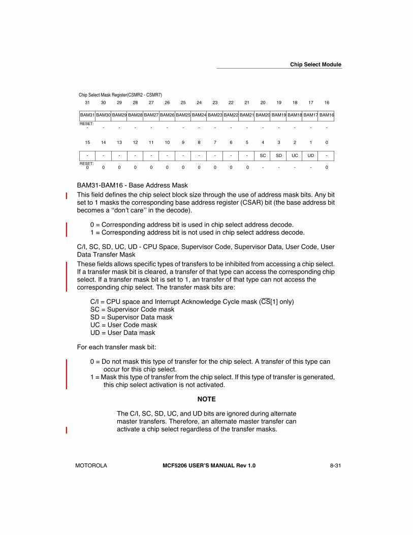
Chip Select Module
MOTOROLA MCF5206 USERÕS MANUAL Rev 1.0 8-31
BAM31-BAM16 - Base Address MaskThis field defines the chip select block size through the use of address mask bits. Any bit set to 1 masks the corresponding base address register (CSAR) bit (the base address bit becomes a ÔÔdonÕt careÕÕ in the decode).
0 = Corresponding address bit is used in chip select address decode.1 = Corresponding address bit is not used in chip select address decode.
C/I, SC, SD, UC, UD - CPU Space, Supervisor Code, Supervisor Data, User Code, User Data Transfer MaskThese fields allows specific types of transfers to be inhibited from accessing a chip select. If a transfer mask bit is cleared, a transfer of that type can access the corresponding chip select. If a transfer mask bit is set to 1, an transfer of that type can not access the corresponding chip select. The transfer mask bits are:
C/I = CPU space and Interrupt Acknowledge Cycle mask (CS[1] only)SC = Supervisor Code maskSD = Supervisor Data maskUC = User Code maskUD = User Data mask
For each transfer mask bit:
0 = Do not mask this type of transfer for the chip select. A transfer of this type can occur for this chip select.
1 = Mask this type of transfer from the chip select. If this type of transfer is generated, this chip select activation is not activated.
NOTE
The C/I, SC, SD, UC, and UD bits are ignored during alternatemaster transfers. Therefore, an alternate master transfer canactivate a chip select regardless of the transfer masks.
BAM31 BAM30 BAM29 BAM28 BAM27 BAM26 BAM25 BAM24 BAM23 BAM22 BAM21 BAM20 BAM19 BAM18 BAM17 BAM16
31 30 29 28 27 26 25 24 23 22 21 20 19 18 17 16
- - - - - - - - - - - - - - - -RESET:
- - - - - - - - - - - SC SD UC UD -
15 14 13 12 11 10 9 8 7 6 5 4 3 2 1 0
0 0 0 0 0 0 0 0 0 0 0 - - - - 0 RESET:
Chip Select Mask Register(CSMR2 - CSMR7)
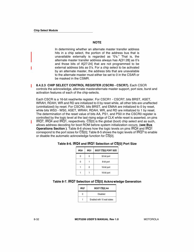
Chip Select Module
8-32 MCF5206 USERÕS MANUAL Rev 1.0 MOTOROLA
NOTE
In determining whether an alternate master transfer addresshits in a chip select, the portion of the address bus that isunavailable externally is regarded as Ò0's.Ó That is, thealternate master transfer address always has A[31:28] as 0Õsand those bits of A[27:24] that are not programmed to beexternal address bits as 0Õs. For a chip select to be activatedby an alternate master, the address bits that are unavailableto the alternate master must either be set to 0 in the CSAR orbe masked in the CSMR.
8.4.2.3 CHIP SELECT CONTROL REGISTER (CSCR0 - CSCR7). Each CSCR controls the acknowledge, alternate masteralternate master support, port size, burst and activation features of each of the chip-selects.
Each CSCR is a 16-bit read/write register. For CSCR1 - CSCR7, bits BRST, ASET, WRAH, RDAH, WR and RD are initialized to 0 by reset while, all other bits are unaffected (uninitialized) by reset. For CSCR0, bits BRST, and EMAA are initialized to 0 by reset, while bits WS3 - WS0, ASET, WRAH, RDAH, WR, and RD are initialized to 1 by reset. The determination of the reset value of bits AA, PS1, and PS0 in the CSCR0 register is controlled by the logic level at the last rising edge of CLK while reset is asserted, on pins IRQ7, IRQ4 and IRQ1, respectively. CS[0] is the global (boot) chip select and as such, allows address decoding for boot ROM before system initialization occurs. (see Bus Operations Section ). Table 8-6 shows how the logic levels on pins IRQ4 and IRQ1 correspond to the port sizes for CS[0]; Table 8-5 shows the logic levels of IRQ7 to enable or disable the automatic acknowledge function for CS[0].
Table 8-6. IRQ4 and IRQ1 Selection of CS[0] Port Size
IRQ4 IRQ1 BOOT CS[0] PORT SIZE
0 0 32-bit port
0 1 8-bit port
1 0 16-bit port
1 1 16-bit port
Table 8-7. IRQ7 Selection of CS[0] Acknowledge Generation
IRQ7 BOOT CS[0] AA
0 Disabled
1 Enabled with 15 wait states

Chip Select Module
MOTOROLA MCF5206 USERÕS MANUAL Rev 1.0 8-33
WS[3:0] - Wait StatesOn accesses initiated by the ColdFire core when AA=1, this field defines the number of wait states inserted before an internal transfer acknowledge is generated. If TA is asserted by the external system before the indicated number of wait states are generated, the assertion of TA ends the cycle.
On accesses initiated by an alternate master when EMAA=1, this field defines the number of waits states inserted before TA is asserted.
BRST - Burst EnableThis field specifies the burst capability of the memory associated with each chip select.
0 = Break all transfers that are larger than the specified port size into individual non-burst transfers that are no larger than the specified port size (e.g. a longword transfer to an 8-bit port would be broken into four individual byte transfers)
1 = Allow burst transfers to the chip-selected address space for all transfers that are larger than the specified port size(e.g. longword transfers to 8- and 16-bit ports, word transfers to 8-bit ports as well as line transfers to 8-, 16- and 32-bit ports)
- - WS3 WS2 WS1 WS0 BRST AA PS1 PS0 EMAA ASET WRAH RDAH WR RD
15 14 13 12 11 10 9 8 7 6 5 4 3 2 1 0
0 0 1 1 1 1 0 IRQ7 IRQ4 IRQ1 0 1 1 1 1 1RESET:
Chip Select Control Register(CSCR0) Address MBAR + $6E
- - WS3 WS2 WS1 WS0 BRST AA PS1 PS0 EMAA ASET WRAH RDAH WR RD
15 14 13 12 11 10 9 8 7 6 5 4 3 2 1 0
0 0 - - - - 0 - - - - 0 0 0 0 0RESET:
Chip Select Control Register(CSCR1-7)

Chip Select Module
8-34 MCF5206 USERÕS MANUAL Rev 1.0 MOTOROLA
AA - Auto Acknowledge Enable for ColdFire core initiated TransfersThis field controls the assertion of the internal transfer acknowledge during accesses initiated by the ColdFire core that hit in the corresponding chip select address space.
0 = Wait for external transfer acknowledge for accesses initiated by the ColdFire core1 = Generate internal transfer acknowledge with the number of wait states specified
by WS[3:0] for accesses initiated by the ColdFire core.
If AA=1 and TA is asserted by the external system before the indicated number of wait states are generated, the external transfer acknowledge ends the transfer.
PS[1:0] - Port SizeThis field specifies the width of the data associated with each chip select. It determines which byte lanes are driven with valid data during write cycles and which byte lanes are sampled for valid data during read cycles.
EMAA - Alternate Master Automatic Acknowledge EnableThis field controls the driving and assertion of TA during accesses initiated by an alternate master that hit in the corresponding chip select address space.
0 = Do not drive TA as an output during accesses initiated by an alternate master and wait for external transfer acknowledge
1 = Drive TA as an output for accesses initiated by an alternate master and insert the number of wait states specified by WS[3:0]
NOTEBecause TA is an output when EMAA = 1, TA must not bedriven by the external system. If TA is asserted by the externalsystem during alternate master transfer and EMAA = 1,damage to the part could occur. Refer to the Bus OperationsSection for more information on the assertion and driving ofTA during alternate master accesses.
Table 8-8. Port Size Encodings
PS[1:0] PORT WIDTH PORTION OF DATA BUS USED
00 32-bit port D[31:0]01 8-bit port D[31:24]10 16-bit port D[31:16]11 16-bit port D[31:16]

Chip Select Module
MOTOROLA MCF5206 USERÕS MANUAL Rev 1.0 8-35
ASET - Address Setup EnableThis field controls the assertion of chip select with respect to assertion of a valid address.
0 = Assert chip select on the rising edge of CLK that address is asserted. See Figure 8-11.
1 = Delay assertion of chip select for one CLK cycle after address is asserted. See Figure 8-12.
Figure 8-11. Chip Select and Write-Enable Assertion with ASET = 0 Timing
Figure 8-12. Chip Select and Write-Enable Assertion with ASET = 1Timing
NOTE
WE asserts one clock after the assertion of CS. During writetransfers, if ASET = 1, both CS and WE are delayed by oneclock.
CLK
TS
ADDR
CS
WE
CLK
TS
ADDR
CS
WE

Chip Select Module
8-36 MCF5206 USERÕS MANUAL Rev 1.0 MOTOROLA
WRAH - Write Address Hold EnableThis field controls the address, data and attribute hold time after the termination (TA, ATA, TEA, or internal transfer acknowledge) of a write cycle that hits in the chip select address space. 0 = Do not hold address, data, and attribute signals an extra cycle after CS and WE negate on writes. See Figure 8-13.
1 = Hold address, data, and attribute signals one cycle after CS and WE negate on writes. See Figure 8-14.
Figure 8-13. Address Hold Timing with WRAH = 0.
Figure 8-14. Address Hold Timing with WRAH = 1
CLK
TS
ADDR
R/W
CS
WE
TA
DATA
ATTR
CLK
TS
ADDR
R/W
CS
WE
TA
DATA
ATTR

Chip Select Module
MOTOROLA MCF5206 USERÕS MANUAL Rev 1.0 8-37
RDAH - Read Address Hold EnableThis field controls the address and attribute hold time after the termination (TA, ATA, TEA or internal transfer acknowledge) during a read cycle that hits in the chip select address space.
0 = Do not hold address and attributes an extra cycle after CS negates on reads. See Figure 8-15.
1 = Hold address and attributes one cycle after CS negates on reads. SeeFigure 8-16.
Figure 8-15. Address Hold Timing with RDAH = 0
CLK
TS
ADDR
R/W
CS
WE
TA
DATA
ATTR
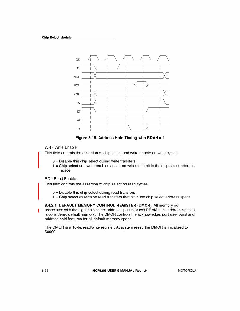
Chip Select Module
8-38 MCF5206 USERÕS MANUAL Rev 1.0 MOTOROLA
Figure 8-16. Address Hold Timing with RDAH = 1
WR - Write EnableThis field controls the assertion of chip select and write enable on write cycles.
0 = Disable this chip select during write transfers1 = Chip select and write enables assert on writes that hit in the chip select address
space
RD - Read EnableThis field controls the assertion of chip select on read cycles.
0 = Disable this chip select during read transfers1 = Chip select asserts on read transfers that hit in the chip select address space
8.4.2.4 DEFAULT MEMORY CONTROL REGISTER (DMCR). All memory not associated with the eight chip select address spaces or two DRAM bank address spaces is considered default memory. The DMCR controls the acknowledge, port size, burst and address hold features for all default memory space.
The DMCR is a 16-bit read/write register. At system reset, the DMCR is initialized to $0000.
CLK
TS
ADDR
R/W
CS
WE
TA
DATA
ATTR
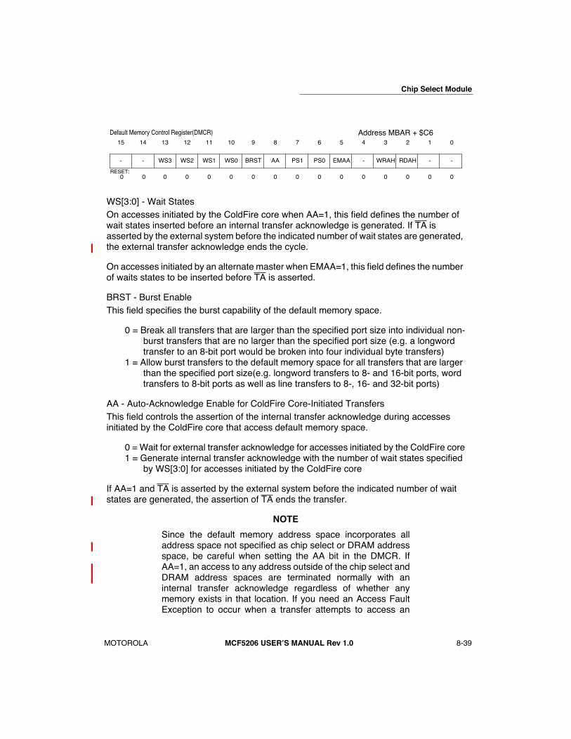
Chip Select Module
MOTOROLA MCF5206 USERÕS MANUAL Rev 1.0 8-39
WS[3:0] - Wait StatesOn accesses initiated by the ColdFire core when AA=1, this field defines the number of wait states inserted before an internal transfer acknowledge is generated. If TA is asserted by the external system before the indicated number of wait states are generated, the external transfer acknowledge ends the cycle.
On accesses initiated by an alternate master when EMAA=1, this field defines the number of waits states to be inserted before TA is asserted.
BRST - Burst EnableThis field specifies the burst capability of the default memory space.
0 = Break all transfers that are larger than the specified port size into individual non-burst transfers that are no larger than the specified port size (e.g. a longword transfer to an 8-bit port would be broken into four individual byte transfers)
1 = Allow burst transfers to the default memory space for all transfers that are larger than the specified port size(e.g. longword transfers to 8- and 16-bit ports, word transfers to 8-bit ports as well as line transfers to 8-, 16- and 32-bit ports)
AA - Auto-Acknowledge Enable for ColdFire Core-Initiated TransfersThis field controls the assertion of the internal transfer acknowledge during accesses initiated by the ColdFire core that access default memory space.
0 = Wait for external transfer acknowledge for accesses initiated by the ColdFire core1 = Generate internal transfer acknowledge with the number of wait states specified
by WS[3:0] for accesses initiated by the ColdFire core
If AA=1 and TA is asserted by the external system before the indicated number of wait states are generated, the assertion of TA ends the transfer.
NOTE
Since the default memory address space incorporates alladdress space not specified as chip select or DRAM addressspace, be careful when setting the AA bit in the DMCR. IfAA=1, an access to any address outside of the chip select andDRAM address spaces are terminated normally with aninternal transfer acknowledge regardless of whether anymemory exists in that location. If you need an Access FaultException to occur when a transfer attempts to access an
- - WS3 WS2 WS1 WS0 BRST AA PS1 PS0 EMAA - WRAH RDAH - -
15 14 13 12 11 10 9 8 7 6 5 4 3 2 1 0
0 0 0 0 0 0 0 0 0 0 0 0 0 0 0 0RESET:
Address MBAR + $C6Default Memory Control Register(DMCR)
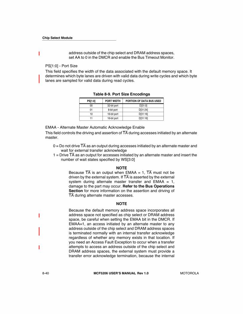
Chip Select Module
8-40 MCF5206 USERÕS MANUAL Rev 1.0 MOTOROLA
address outside of the chip select and DRAM address spaces,set AA to 0 in the DMCR and enable the Bus Timeout Monitor.
PS[1:0] - Port SizeThis field specifies the width of the data associated with the default memory space. It determines which byte lanes are driven with valid data during write cycles and which byte lanes are sampled for valid data during read cycles.
EMAA - Alternate Master Automatic Acknowledge EnableThis field controls the driving and assertion of TA during accesses initiated by an alternate master.
0 = Do not drive TA as an output during accesses initiated by an alternate master and wait for external transfer acknowledge
1 = Drive TA as an output for accesses initiated by an alternate master and insert the number of wait states specified by WS[3:0]
NOTEBecause TA is an output when EMAA = 1, TA must not bedriven by the external system. If TA is asserted by the externalsystem during alternate master transfer and EMAA = 1,damage to the part may occur. Refer to the Bus OperationsSection for more information on the assertion and driving ofTA during alternate master accesses.
NOTE
Because the default memory address space incorporates alladdress space not specified as chip select or DRAM addressspace, be careful when setting the EMAA bit in the DMCR. IfEMAA=1, an access initiated by an alternate master to anyaddress outside of the chip select and DRAM address spacesis terminated normally with an internal transfer acknowledgeregardless of whether any memory exists in that location. Ifyou need an Access Fault Exception to occur when a transferattempts to access an address outside of the chip select andDRAM address spaces, the external system must provide atransfer error acknowledge termination, because the internal
Table 8-9. Port Size Encodings
PS[1:0] PORT WIDTH PORTION OF DATA BUS USED
00 32-bit port D[31:0]01 8-bit port D[31:24]10 16-bit port D[31:16]11 16-bit port D[31:16]
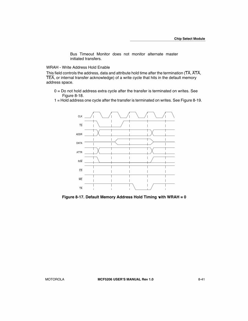
Chip Select Module
MOTOROLA MCF5206 USERÕS MANUAL Rev 1.0 8-41
Bus Timeout Monitor does not monitor alternate masterinitiated transfers.
WRAH - Write Address Hold EnableThis field controls the address, data and attribute hold time after the termination (TA, ATA, TEA, or internal transfer acknowledge) of a write cycle that hits in the default memory address space.
0 = Do not hold address extra cycle after the transfer is terminated on writes. See Figure 8-18.
1 = Hold address one cycle after the transfer is terminated on writes. See Figure 8-19.
Figure 8-17. Default Memory Address Hold Timing with WRAH = 0
CLK
TS
ADDR
R/W
CS
WE
TA
DATA
ATTR
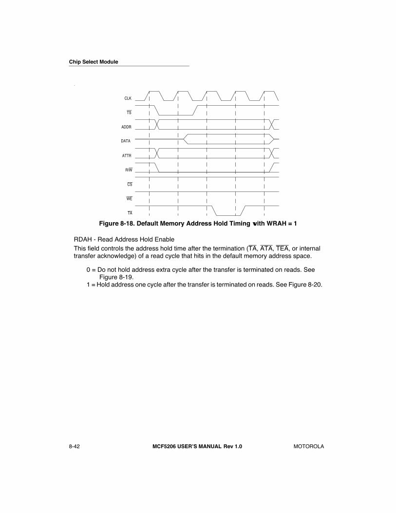
Chip Select Module
8-42 MCF5206 USERÕS MANUAL Rev 1.0 MOTOROLA
.
Figure 8-18. Default Memory Address Hold Timing with WRAH = 1
RDAH - Read Address Hold EnableThis field controls the address hold time after the termination (TA, ATA, TEA, or internal transfer acknowledge) of a read cycle that hits in the default memory address space.
0 = Do not hold address extra cycle after the transfer is terminated on reads. See Figure 8-19.
1 = Hold address one cycle after the transfer is terminated on reads. See Figure 8-20.
CLK
TS
ADDR
R/W
CS
WE
TA
DATA
ATTR

Chip Select Module
MOTOROLA MCF5206 USERÕS MANUAL Rev 1.0 8-43
Figure 8-19. Default Memory Address Hold Timing with RDAH = 0
Figure 8-20. Default Memory Address Hold Timing with RDAH = 1
CLK
TS
ADDR
R/W
CS
WE
TA
DATA
ATTR
CLK
TS
ADDR
R/W
CS
WE
TA
DATA
ATTR

MOTOROLA
MCF5206 USERÕS MANUAL Rev 1.0
9-1
2
3
4
5
6
7
8
9
10
11
12
13
14
15
16
1
SECTION 9PARALLEL PORT (GENERAL-PURPOSE I/O) MODULE
9.1 INTRODUCTION
The MCF5206 provides eight general-purpose input/output signals that can be used on a pin-by-pin basis. This subsection describes the operation and programming model of the parallel port registers and the direction-control and data registers.
9.2 PARALLEL PORT OPERATION
The MCF5206 parallel port module has eight signals that you can select as inputs or outputs on a pin-by-pin basis. These pins are multiplexed with the MCF5206 emulation pins and are programmed to their parallel port function through the Pin Assignment Register (PAR). Refer to the SIM subsection
6.3.2.10
Pin Assignment Register
for programming description.
9.3 PROGRAMMING MODEL
9.3.1 Parallel Port Registers Memory Map
Table 9-1 shows the memory map of all the parallel port registers. The internal registers in the parallel port module are memory-mapped registers offset from the MBAR address pointer. Refer to the SIM section for programming of the MBAR.
The following key notes apply to the programming model table:
¥ Addresses not assigned to a register and undefined register bits are reserved for future expansion. Write accesses to these reserved address spaces and reserved register bits have no effect; read accesses return zeros.
¥ The reset value column indicates the register initial value at reset. Certain registers can be uninitialized at reset.
¥ The access column indicates if the corresponding register allows both read/write functionality (R/W), read-only functionality (R), or write-only functionality (W). Any read-access attempts to a write-only register return zeros. A write access to a read-only register attempt is ignored and no write occurs.
Table 9-1. Memory Map of Parallel Port Registers
ADDRESS NAME WIDTH DESCRIPTION RESET VALUE ACCESS
MBAR + $1C5 PPDDR 8 Port A Data Direction Register $00 R/W
MBAR + $1C9 PPDAT 8 Port A Data Register $00 R/W
DATE: 9-2-98
REVISION NO.: 1.1
PAGES AFFECTED: SEE CHANGE BARS

Parallel Port (General-Purpose I/O) Module
9-2
MCF5206 USERÕS MANUAL Rev 1.0
MOTOROLA
2
3
4
5
6
7
9
10
11
12
13
14
15
16
1
9.3.2 Parallel Port Registers
9.3.2.1 PORT A DATA DIRECTION REGISTER (PADDR).
The data direction register allows you to select the signal direction of each parallel port signal. There is one DDR bit in the PADDR for each parallel port signal. The data direction control bits only affect the direction of the associated pin if you program that pin as a general- purpose I/O signal in the PAR. Refer to SIM subsection
6.3.2.10 Pin Assigment Register(PAR)
for programming details.
The DDR is an 8-bit read/write register. At system reset, all bits are initialized to zero.
DDR[7:0] - Data Direction Bits[7:0]For each of the data direction bits, you can select the direction of the signal as follows:
0 = Signal is an input1 = Signal is an output
Table 9-1 indicates how the bits in the data direction register are assigned to the PP[7:4]/DDATA[3:0] and PP[3:0]/PST[3:0] signal pins.
9.3.2.2 PORT A DATA REGISTER (PADAT).
The parallel port data register reflects the current status of the parallel port signals. If you configure a parallel port signal as an input, the value in the register corresponds to the logical voltage level present at the pin. If you configure the parallel portsignal as an output, the value in the register corresponds to the logical voltage level driven onto the pin.
Table 9-1. Data Direction Register Bit Assignments
DATA DIRECTION REGISTER BIT OUTPUT PIN
DDR7 PP[7]/DDATA[3]DDR6 PP[6]/DDATA[2]DDR5 PP[5]/DDATA[1]DDR4 PP[4]/DDATA[0]DDR3 PP[3]/PST[3]DDR2 PP[2]/PST[2]DDR1 PP[1]/PST[1]DDR0 PP[0]/PST[0]
DDR7 DDR6 DDR5 DDR4 DDR3 DDR2 DDR1 DDR0
7 6 5 4 3 2 1 0
0 0 0 0 0 0 0 0RESET:
Data Direction Register (DDR) Address MBAR + $1C5
R/W

Parallel Port (General-Purpose I/O) Module
MOTOROLA
MCF5206 USERÕS MANUAL Rev 1.0
9-3
2
3
4
5
6
7
8
9
10
11
12
13
14
15
16
1
The Parallel Port Data Register is an 8-bit read/write register. At system reset, the PADAT is initialized to zeros.
NOTE
Bits in PADAT are valid for the pins configured as general-purpose I/O only. If you configure a pin to output BackgroundDebug mode signals, the value of PADAT is not valid.
NOTE
You can write to the PADAT register at anytime. A write to a bitcorresponding to an input signal seemingly has no affect.However, if a pin change from an input to an output, the valuemost recently WRITTEN into the PADAT is the value driven ontothe pin.
DAT[7:0] - Parallel Port Data Register bits[7:0]Each bit in the Parallel Port Data Register corresponds to a particular signal pin as indicated in Table 9-2. The values in this register are controlled as follows:
¥ For parallel port signals programmed to outputs:
Ñ For PADAT read: register bit indicates logical voltage level at the pinÑ For PADAT write: drive indicated logical voltage level onto associated pin
¥ For parallel port signals programmed to inputs:
Ñ For PADAT read: register bit indicates current logical voltage level of pinÑ For PADAT write: has no affect unless pin direction is changed to output. Refer to
the NOTE above.
Table 9-2. Data Register Bit Assignments
DATA REGISTER BITS OUTPUT PIN
DAT7 PP[7]/DDATA[3]DAT6 PP[6]/DDATA[2]DAT5 PP[5]/DDATA[1]DAT4 PP[4]/DDATA[0]DAT3 PP[3]/PST[3]DAT2 PP[2]/PST[2]DAT1 PP[1]/PST[1]DAT0 PP[0]/PST[0]
DAT7 DAT6 DAT5 DAT4 DAT3 DAT2 DAT1 DAT0
7 6 5 4 3 2 1 0
0 0 0 0 0 0 0 0RESET:
Parallel Port Data Register(PPDAT) Address MBAR + $1C9
R/W
MOTOROLA
MCF5206 USERÕS MANUAL Rev 1.0
10-1
4
5
6
7
8
9
10
11
12
14
15
16
1
SECTION 10DRAM CONTROLLER
10.1 INTRODUCTION
The DRAM controller (DRAMC) provides a glueless interface between the ColdFire core and external DRAM. The DRAMC supports two banks of DRAM. Each DRAM bank can be from 128 KByte to 256 MByte, in widths of 8, 16, or 32 bits. Two row address strobe (RAS[1:0]) signals are provided externally to access the two DRAM banks. Data byte lanes are enabled using the four column address strobe (CAS[3:0]) signals. The DRAM write (DRAMW) signal indicates if the DRAM transfer is a read or a write. The DRAMC handles address multiplexing internally, allowing for a glueless DRAM interface. The DRAMC has an internal refresh timer that generates CAS-before-RAS refresh cycles. You can program RAS and CAS waveform timing and refresh rates. External master use of the DRAMC for accessing the DRAM banks is also supported.
10.1.1 Features
The following list summarizes the key DRAMC features:
¥ Supports two banks of DRAM
¥ Supports Normal Mode, Fast Page Mode, and Burst Page Mode
¥ Supports EDO DRAMs
¥ Supports glueless row address/column address multiplexing
¥ Programmable RAS and CAS timings
¥ Programmable refresh timer for CAS-before-RAS refresh
¥ Supports external master use of the DRAMC
10.2 DRAM CONTROLLER I/O
10.2.1 Control Signals
The DRAMC has seven control signal signals: CAS[0], CAS[1], CAS[2], CAS[3], RAS[0], RAS[1], and DRAMW.
10.2.1.1 ROW ADDRESS STROBES (RAS[0], RAS[1]).
These active-low output signals provide control for the row address strobe (RAS) input pins on industry-standard DRAMs. There is one RAS output for each DRAM bank: RAS[0] controls DRAM bank 0 and RAS[1] controls DRAM bank 1. RAS timing can be customized to match the specifications of the DRAM being used by programming the DRAMC Timing Register (see
Section 10.4.2.2 DRAM Controller Timing Register (DCTR)
).
DATE: 9-2-98
REVISION NO.: 1.1
PAGES AFFECTED: SEE CHANGE BARS

2
3
4
5
6
7
8
9
10
11
12
13
14
15
16
1
DRAM Controller
10-2
MCF5206 USERÕS MANUAL Rev 1.0
MOTOROLA
10.2.1.2 COLUMN ADDRESS STROBES (CAS[0], CAS[1], CAS[2], CAS[3]).
These active-low output signals provide control for the column address strobe (CAS) input pins on industry-standard DRAMs. The CAS signals are used to enable data byte lanes: CAS[0] controls access to D[31:24], CAS[1] to D[23:16], CAS[2] to D[15:8], and CAS[3] to D[7:0]. CAS[3:0] should be used for a 32-bit wide DRAM bank, CAS[1:0] for a 16-bit wide DRAM bank, and CAS[0] for an 8-bit wide DRAM bank. Table 10-1 shows which CAS signals are asserted based on the operand size, the DRAM port size and the address bits A[1:0]. For DRAM transfers SIZ[1:0] always matches the operand size.
Table 10-1. CAS Assertion
OPERAND SIZE PORT SIZE SIZ[1] SIZ[0] A[1] A[0]CAS[0] CAS[1] CAS[2] CAS[3]
D[31:24] D[23:16] D[15:8] D[7:0]
BYTE
8-BIT 0 1
0 0 0 1 1 1
0 1 0 1 1 1
1 0 0 1 1 1
1 1 0 1 1 1
16-BIT 0 1
0 0 0 1 1 1
0 1 1 0 1 1
1 0 0 1 1 1
1 1 1 0 1 1
32-BIT 0 1
0 0 0 1 1 1
0 1 1 0 1 1
1 0 1 1 0 1
1 1 1 1 1 0
WORD
8-BIT 1 0
0 0 0 1 1 1
0 1 0 1 1 1
1 0 0 1 1 1
1 1 0 1 1 1
16-BIT 1 00 0 0 0 1 1
1 0 0 0 1 1
32-BIT 1 00 0 0 0 1 1
1 0 1 1 0 0
LONG WORD
8-BIT 0 0
0 0 0 1 1 1
0 1 0 1 1 1
1 0 0 1 1 1
1 1 0 1 1 1
16-BIT 0 00 0 0 0 1 1
1 0 0 0 1 1
32-BIT 0 0 0 0 0 0 0 0

DRAM Controller
MOTOROLA
MCF5206 USERÕS MANUAL Rev 1.0
10-3
2
3
4
5
6
7
8
9
10
11
12
13
14
15
16
1
CAS timing can be customized to match the specifications of the DRAM by programming the DRAM Controller Timing Register (see
Section 10.4.2.2 DRAM Controller Timing Register (DCTR)
).
10.2.1.3 DRAM WRITE (DRAMW).
This active-low output signal is asserted during DRAM write cycles, and negated during DRAM read cycles. The DRAMW signal is negated during refresh cycles.The DRAMW signal is provided in addition to the R/W signal to allow refreshes to occur during nonDRAM cycles (regardless of the state of the R/W signal). The R/W signal indicates the direction of all bus transfers, while DRAMW is only valid during DRAM transfers.
10.2.2 Address Bus
The address bus includes 24 dedicated address signals, A[23:0], and supports as manyas four additional configurable address signals, A[27:24] (refer to
Section 7.3.2.10 PinAssignment Register (PAR)
). The DRAM address appears only on the pins configuredto be address signals. The maximum size of DRAM that can be connected to each bankis limited by the number of address signals available (see Table 10-2).
For transfers initiated by the ColdFire core, the DRAMC outputs both the row address and the column address, allowing the address bus to be directly connected to external DRAM. The internal address multiplexing can be selectively enabled for transfers initiated by an external master by programming the DAEM bit in the DCTR (see
Section 10.4.2.2 DRAM Controller Timing Register (DCTR)
).
LINE
8-BIT 1 1
0 0 0 1 1 1
0 1 0 1 1 1
1 0 0 1 1 1
1 1 0 1 1 1
16-BIT 1 10 0 0 0 1 1
1 0 0 0 1 1
32-BIT 1 1 0 0 0 0 0 0
Table 10-2. Maximum DRAM Bank Sizes
AVAILABLE ADDRESS SIGNALS
MAXIMUM DRAM SIZE
A[23:0] 16 MByteA[24:0] 32 MByteA[25:0] 64 MByteA[26:0] 128 MByteA[27:0] 256 MByte
Table 10-1. CAS Assertion (Continued)
OPERAND SIZE PORT SIZE SIZ[1] SIZ[0] A[1] A[0]CAS[0] CAS[1] CAS[2] CAS[3]
D[31:24] D[23:16] D[15:8] D[7:0]
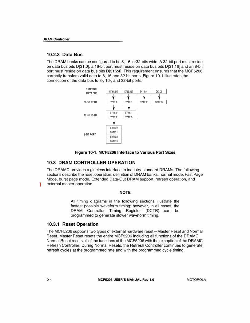
2
3
4
5
6
7
8
9
10
11
12
13
14
15
16
1
DRAM Controller
10-4
MCF5206 USERÕS MANUAL Rev 1.0
MOTOROLA
10.2.3 Data Bus
The DRAM banks can be configured to be 8, 16, or32-bits wide. A 32-bit port must reside on data bus bits D[31:0], a 16-bit port must reside on data bus bits D[31:16] and an 8-bit port must reside on data bus bits D[31:24]. This requirement ensures that the MCF5206 correctly transfers valid data to 8, 16 and 32-bit ports. Figure 10-1 illustrates the connection of the data bus to 8-, 16-, and 32-bit ports.
Figure 10-1. MCF5206 Interface to Various Port Sizes
10.3 DRAM CONTROLLER OPERATION
The DRAMC provides a glueless interface to industry-standard DRAMs. The following sections describe the reset operation, definition of DRAM banks, normal mode, Fast Page Mode, burst page mode, Extended Data-Out DRAM support, refresh operation, and external master operation.
NOTE
All timing diagrams in the following sections illustrate thefastest possible waveform timing; however, in all cases, theDRAM Controller Timing Register (DCTR) can beprogrammed to generate slower waveform timing.
10.3.1 Reset Operation
The MCF5206 supports two types of external hardware resetÑMaster Reset and Normal Reset. Master Reset resets the entire MCF5206 including all functions of the DRAMC. Normal Reset resets all of the functions of the MCF5206 with the exception of the DRAMC Refresh Controller. During Normal Resets, the Refresh Controller continues to generate refresh cycles at the programmed rate and with the programmed cycle timing.
EXTERNAL
DATA BUS
BYTE 0
8-BIT PORT
16-BIT PORT
32-BIT PORT
BYTE 1
BYTE 2
BYTE 3
BYTE 0 BYTE 1
BYTE 2 BYTE 3
BYTE 0 BYTE 1 BYTE 2 BYTE 3
D[31:24] D[23:16] D[15:8] D[7:0]

DRAM Controller
MOTOROLA
MCF5206 USERÕS MANUAL Rev 1.0
10-5
2
3
4
5
6
7
8
9
10
11
12
13
14
15
16
1
NOTE
Master Reset must be asserted for all power-on resets. Failureto assert Master Reset on power-on reset could result inunpredictable DRAMC behavior.
10.3.1.1 MASTER RESET.
During a master reset all registers in the DRAMC are initialized to a known state and all DRAMC operation is halted. The DRAM refresh counter does not count and DRAM refresh cycles is not generated. Any DRAM transfer or refresh cycle in progress is immediately terminated.
A master reset is accomplished by asserting and negating the RSTI and HIZ signals simultaneously (see
Section 6.11 Reset Operation
).
NOTE
During a master reset, the DCCR is reset to $000 (giving theslowest refresh rate) and the DCTR is reset to $0000 (givingthe fastest waveform timing). After a Master Reset, the usershould program the DRAMC Refresh Register (DCRR) andthe DRAMC Timing Register (DCTR) such that refresh cyclesare generated at the required rate and with the required timingfor the DRAM in the system. In general, DRAMs require aninitial pause after power-up and require a minimum number ofDRAM cycles to be run before the DRAM is ready for use. ThisÒwake-upÓ sequence must be handled via software.
10.3.1.2 NORMAL RESET.
Normal reset is used when the DRAM contains valid data which needs to be maintained through reset. The DRAMC Refresh Register (DCRR), DRAMC Timing Register (DCTR), and the internal DRAMC Refresh controller are unaffected by normal reset. All other MCF5206 registers are reset to the same values during normal resets as during Master Resets. During normal reset, DRAM refreshes occur at the programmed rate and with the programmed DRAM cycle timing.
A normal reset is accomplished by asserting the RSTI signal while negating the HIZ signal. Resets generated by the internal Software Watchdog Timer are normal resets.
10.3.2 Definition of DRAM Banks
The DRAMC supports as many as two banks of DRAM. You can program each bank independently except for the RAS and CAS waveform timing (programming the DCTR affects the waveform timing for both banks).
10.3.2.1 BASE ADDRESS AND ADDRESS MASKING.
The transfer address generated by the ColdFire core or by an external master is compared to the unmasked bits of the base address programmed for each bank in the DRAMC Address Registers (DCAR0 - DCAR1). The bits that are masked is determined by the value programmed in the BAM field in the DRAMC Mask Registers (DCMR0 - DCMR1).

2
3
4
5
6
7
8
9
10
11
12
13
14
15
16
1
DRAM Controller
10-6
MCF5206 USERÕS MANUAL Rev 1.0
MOTOROLA
The masking of address bits is used to define the address space of the DRAM bank. Address bits that are masked are not used in the comparison with the transfer address. The base address field (BA31-BA17) in the DCARs and the base address mask field (BAM31-BAM17) in the DCMRs correspond to transfer address bits 31-17. Clearing (unmasking) all bits in the BAM field makes the address space 128 KByte. For the address space of a DRAM bank to be contiguous, address bits should be masked (BAM bits set to a 1) in ascending order starting with A[17].
For example, if the DCARs and DCMRs are programmed as shown in Table 10-3, DRAM bank 0 would have a 16 MByte address space starting at address $04000000, while DRAM bank 1 would have a 1 MByte address space starting at address $05000000. A transfer with A[31:24] = $04 accesses DRAM bank 0, and a transfer address with A[31:20] = $050 accesses DRAM bank 1.
Refer to
Section 10.4.2.3 DRAM Controller Address Registers (DCAR0 - DCAR1)
and
Section 10.4.2.4 DRAM Controller Mask Register (DCMR0 - DCMR1)
for further details.
NOTE
The ColdFire core outputs 32 bits of address to the internalbus controller. Of these 32 bits, only A[27:0] are output to pinson the MCF5206. The output of A[27:24] are dependent on thesetting of PAR3-PAR0 in the Pin Assignment Register (PAR)in the SIM.
NOTE
The MCF5206 compares the address for the current bustransfer with the address and mask bits in the Chip SelectAddress Registers (CSARs), DRAM Controller AddressRegisters (DCARs) and the Chip Select Mask Register
Table 10-3. DRAM Bank Programming Example 1
DRAM BANK DCAR DCMRDRAM ADDRESS
SPACEADDRESS MATCH
0 $0400 $00FE0000 16 MByte $04xxxxxx1 $0500 $000E0000 1 MByte $050xxxxx
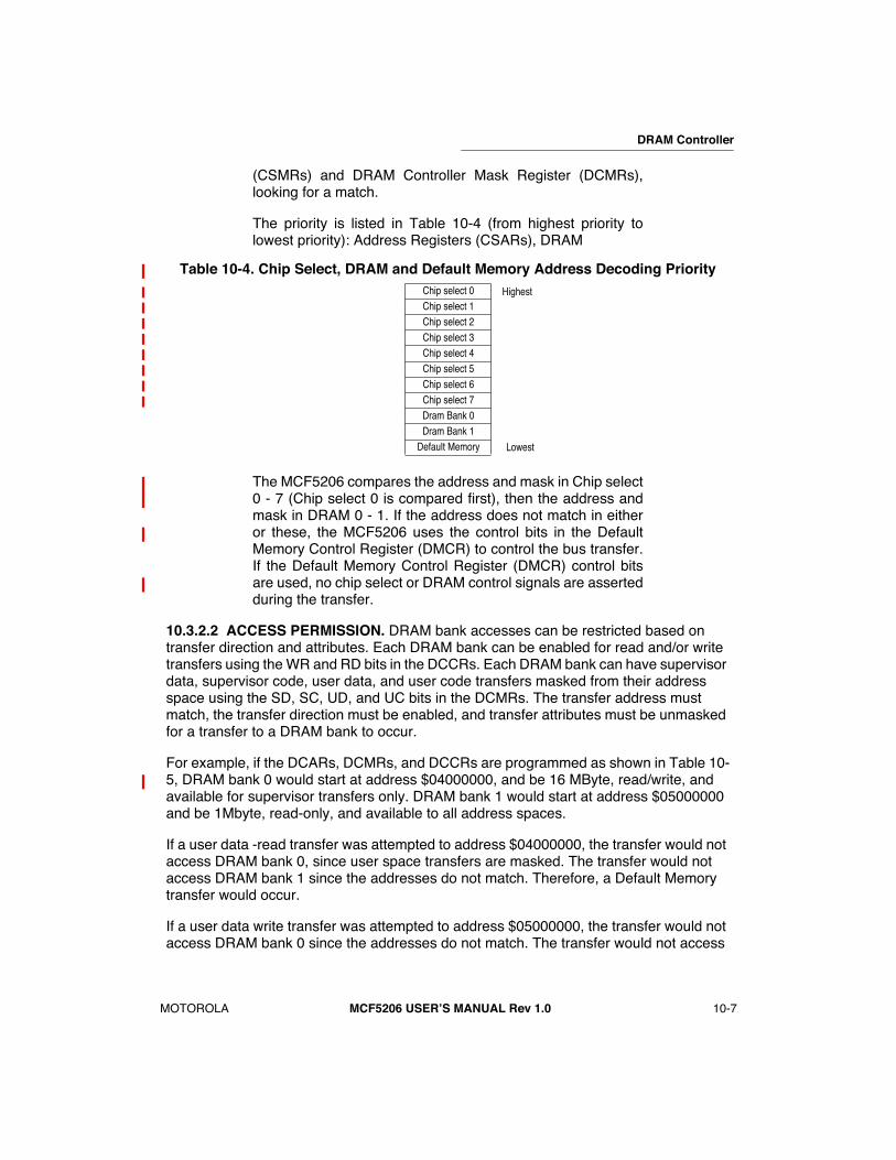
DRAM Controller
MOTOROLA
MCF5206 USERÕS MANUAL Rev 1.0
10-7
2
3
4
5
6
7
8
9
10
11
12
13
14
15
16
1
(CSMRs) and DRAM Controller Mask Register (DCMRs),looking for a match.
The priority is listed in Table 10-4 (from highest priority tolowest priority): Address Registers (CSARs), DRAM
The MCF5206 compares the address and mask in Chip select0 - 7 (Chip select 0 is compared first), then the address andmask in DRAM 0 - 1. If the address does not match in eitheror these, the MCF5206 uses the control bits in the DefaultMemory Control Register (DMCR) to control the bus transfer.If the Default Memory Control Register (DMCR) control bitsare used, no chip select or DRAM control signals are assertedduring the transfer.
10.3.2.2 ACCESS PERMISSION.
DRAM bank accesses can be restricted based on transfer direction and attributes. Each DRAM bank can be enabled for read and/or write transfers using the WR and RD bits in the DCCRs. Each DRAM bank can have supervisor data, supervisor code, user data, and user code transfers masked from their address space using the SD, SC, UD, and UC bits in the DCMRs. The transfer address must match, the transfer direction must be enabled, and transfer attributes must be unmasked for a transfer to a DRAM bank to occur.
For example, if the DCARs, DCMRs, and DCCRs are programmed as shown in Table 10-5, DRAM bank 0 would start at address $04000000, and be 16 MByte, read/write, and available for supervisor transfers only. DRAM bank 1 would start at address $05000000 and be 1Mbyte, read-only, and available to all address spaces.
If a user data -read transfer was attempted to address $04000000, the transfer would not access DRAM bank 0, since user space transfers are masked. The transfer would not access DRAM bank 1 since the addresses do not match. Therefore, a Default Memory transfer would occur.
If a user data write transfer was attempted to address $05000000, the transfer would not access DRAM bank 0 since the addresses do not match. The transfer would not access
Table 10-4. Chip Select, DRAM and Default Memory Address Decoding Priority
Chip select 0Chip select 1Chip select 2Chip select 3Chip select 4Chip select 5Chip select 6Chip select 7Dram Bank 0Dram Bank 1
Default Memory
Highest
Lowest

2
3
4
5
6
7
8
9
10
11
12
13
14
15
16
1
DRAM Controller
10-8
MCF5206 USERÕS MANUAL Rev 1.0
MOTOROLA
DRAM bank 1 since this bank is not enabled for writes. Therefore, a Default Memory transfer would occur.
Refer to
Section 10.4.2.4 DRAM Controller Mask Register (DCMR0 - DCMR1)
and
Section 10.4.2.5 DRAM Controller Control Register (DCCR0 - DCCR1)
for further details.
10.3.2.3 TIMING.
The timing of RAS and CAS assertion and negation can be customized to meet the timing specifications for the specific DRAM being used. This programmed waveform timing is used for both banks.
Refer to
Section 10.4.2.2 DRAM Controller Timing Register (DCTR)
for further details.
10.3.2.4 PAGE MODE.
Each bank can be configured for normal mode, fast page mode, or burst page mode. Normal mode DRAM cycles supply a row address and a column address for each transfer. Fast page mode DRAM cycles supply a row address and a column address for the first transfer to a page and only a column address on successive transfers to that page. Burst page mode is a combination of normal mode and fast page mode. For transfers where the port size is larger or the same as the operand size (non-burst transfers), burst page mode operates the same as normal mode. For transfers where the operand size is larger than the port size (burst transfers), burst page mode operates the same as fast page mode.
Refer to
10.3.3 Normal Mode Operation
,
10.3.4 Fast Page Mode Operation
,
10.3.5 Burst Page-Mode Operation
, and
Section 10.4.2.5 DRAM Controller Control Register (DCCR0 - DCCR1)
for further details.
10.3.2.5 PORT SIZE/PAGE SIZE.
Each DRAM bank can be programmed for 8-, 16-, or 32-bit port sizes. Each bank can also have an internal bank page size of 512 byte, 1 KByte, or 2 KByte.
Refer to
Section 10.4.2.5 DRAM Controller Control Register (DCCR0 - DCCR1)
for further details.
10.3.2.6 ADDRESS MULTIPLEXING.
The MCF5206 provides internal address multiplexing of the row address and column address for DRAM transfers. The internal address multiplexing is used for all ColdFire core initiated DRAM transfers and can selectively be used for external master initiated DRAM transfers. No external logic is required in the system to handle DRAM address multiplexing when the internal multiplexing is used. In addition, the multiplexing scheme allows a single printed circuit board layout to support multiple DRAM memory sizes (allowing for easy memory upgrades).
Table 10-5. DRAM Bank Programming Example 2
DRAM BANK DCAR DCMR DCCR ADDRESS MATCH TRANSFER TYPE READ/WRITE
0 $0400 $00FE0006 $03 $04xxxxxx supervisor-only read/write1 $0500 $000E0000 $01 $050xxxxx all transfer types read-only
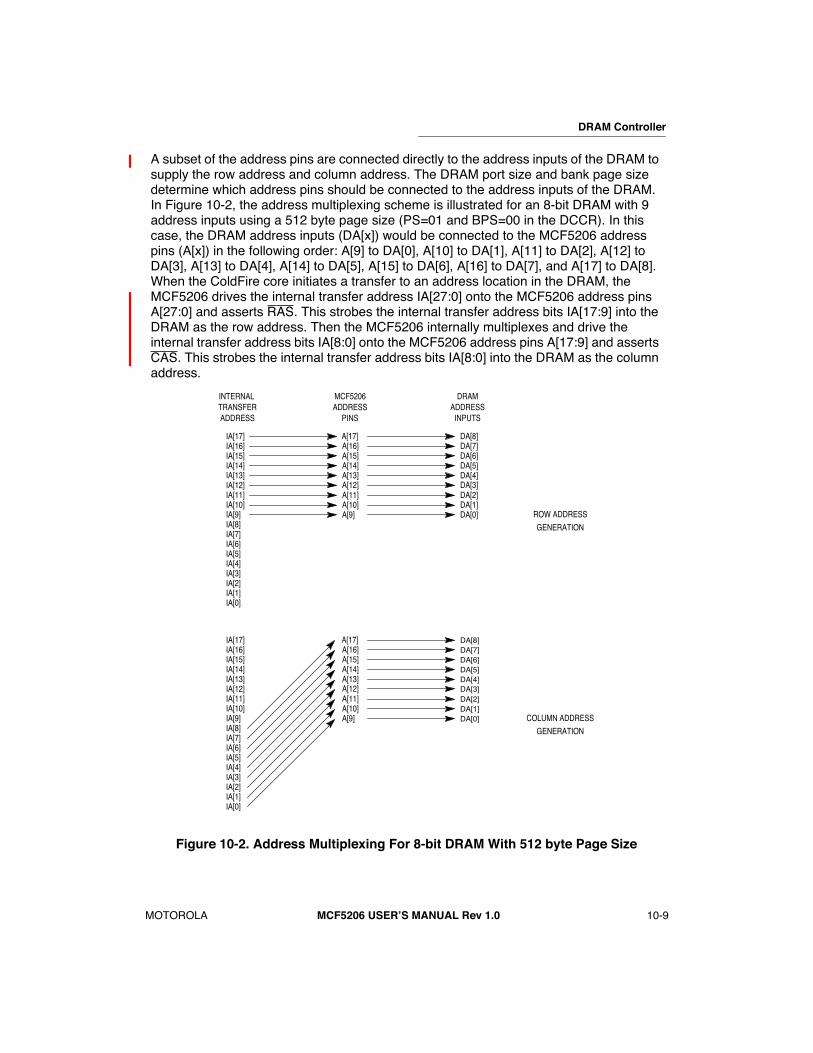
DRAM Controller
MOTOROLA
MCF5206 USERÕS MANUAL Rev 1.0
10-9
2
3
4
5
6
7
8
9
10
11
12
13
14
15
16
1
A subset of the address pins are connected directly to the address inputs of the DRAM to supply the row address and column address. The DRAM port size and bank page size determine which address pins should be connected to the address inputs of the DRAM. In Figure 10-2, the address multiplexing scheme is illustrated for an 8-bit DRAM with 9 address inputs using a 512 byte page size (PS=01 and BPS=00 in the DCCR). In this case, the DRAM address inputs (DA[x]) would be connected to the MCF5206 address pins (A[x]) in the following order: A[9] to DA[0], A[10] to DA[1], A[11] to DA[2], A[12] to DA[3], A[13] to DA[4], A[14] to DA[5], A[15] to DA[6], A[16] to DA[7], and A[17] to DA[8]. When the ColdFire core initiates a transfer to an address location in the DRAM, the MCF5206 drives the internal transfer address IA[27:0] onto the MCF5206 address pins A[27:0] and asserts RAS. This strobes the internal transfer address bits IA[17:9] into the DRAM as the row address. Then the MCF5206 internally multiplexes and drive the internal transfer address bits IA[8:0] onto the MCF5206 address pins A[17:9] and asserts CAS. This strobes the internal transfer address bits IA[8:0] into the DRAM as the column address.
Figure 10-2. Address Multiplexing For 8-bit DRAM With 512 byte Page Size
IA[17]IA[16]IA[15]IA[14]IA[13]IA[12]IA[11]IA[10]IA[9]
A[17]A[16]A[15]A[14]A[13]A[12]A[11]A[10]A[9]
DA[8]DA[7]DA[6]DA[5]DA[4]DA[3]DA[2]DA[1]DA[0]
IA[8]IA[7]IA[6]IA[5]IA[4]IA[3]IA[2]IA[1]IA[0]
IA[17]IA[16]IA[15]IA[14]IA[13]IA[12]IA[11]IA[10]IA[9]
A[17]A[16]A[15]A[14]A[13]A[12]A[11]A[10]A[9]
DA[8]DA[7]DA[6]DA[5]DA[4]DA[3]DA[2]DA[1]DA[0]
IA[8]IA[7]IA[6]IA[5]IA[4]IA[3]IA[2]IA[1]IA[0]
INTERNAL TRANSFERADDRESS
MCF5206ADDRESS
PINS
DRAMADDRESS
INPUTS
ROW ADDRESS
GENERATION
COLUMN ADDRESS
GENERATION

2
3
4
5
6
7
8
9
10
11
12
13
14
15
16
1
DRAM Controller
10-10
MCF5206 USERÕS MANUAL Rev 1.0
MOTOROLA
The port size (PS) and the bank page size (BPS) determine which address bus pins are used to drive the row address and column address. Table 10-6, Table 10-7, and Table 10-8 show which internal transfer address bits are driven on each address pin during the assertion of RAS and during the assertion of CAS for all combinations of port size (PS) and bank page size (BPS). The shaded address pins in each PS/BPS configuration outputs the row address during the assertion of RAS and the column address during the assertion of CAS. These signals should be connected to the DRAM address inputs. The number of address signals used depends on the size of the DRAM. Because byte CAS signals (CAS[3:0]) are provided, A[0] is unnecessary for 16-bit DRAMs and A[1:0] are unnecessary for 32-bit DRAMs.
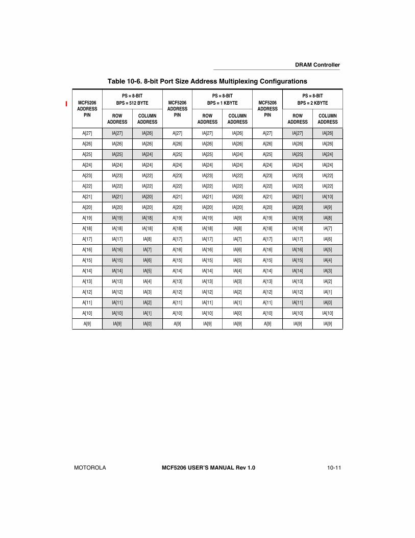
DRAM Controller
MOTOROLA
MCF5206 USERÕS MANUAL Rev 1.0
10-11
2
3
4
5
6
7
8
9
10
11
12
13
14
15
16
1
Table 10-6. 8-bit Port Size Address Multiplexing Configurations
MCF5206 ADDRESS
PIN
PS = 8-BITBPS = 512 BYTE MCF5206
ADDRESS PIN
PS = 8-BITBPS = 1 KBYTE MCF5206
ADDRESS PIN
PS = 8-BITBPS = 2 KBYTE
ROW ADDRESS
COLUMN ADDRESS
ROW ADDRESS
COLUMN ADDRESS
ROW ADDRESS
COLUMN ADDRESS
A[27] IA[27] IA[26] A[27] IA[27] IA[26] A[27] IA[27] IA[26]
A[26] IA[26] IA[26] A[26] IA[26] IA[26] A[26] IA[26] IA[26]
A[25] IA[25] IA[24] A[25] IA[25] IA[24] A[25] IA[25] IA[24]
A[24] IA[24] IA[24] A[24] IA[24] IA[24] A[24] IA[24] IA[24]
A[23] IA[23] IA[22] A[23] IA[23] IA[22] A[23] IA[23] IA[22]
A[22] IA[22] IA[22] A[22] IA[22] IA[22] A[22] IA[22] IA[22]
A[21] IA[21] IA[20] A[21] IA[21] IA[20] A[21] IA[21] IA[10]
A[20] IA[20] IA[20] A[20] IA[20] IA[20] A[20] IA[20] IA[9]
A[19] IA[19] IA[18] A[19] IA[19] IA[9] A[19] IA[19] IA[8]
A[18] IA[18] IA[18] A[18] IA[18] IA[8] A[18] IA[18] IA[7]
A[17] IA[17] IA[8] A[17] IA[17] IA[7] A[17] IA[17] IA[6]
A[16] IA[16] IA[7] A[16] IA[16] IA[6] A[16] IA[16] IA[5]
A[15] IA[15] IA[6] A[15] IA[15] IA[5] A[15] IA[15] IA[4]
A[14] IA[14] IA[5] A[14] IA[14] IA[4] A[14] IA[14] IA[3]
A[13] IA[13] IA[4] A[13] IA[13] IA[3] A[13] IA[13] IA[2]
A[12] IA[12] IA[3] A[12] IA[12] IA[2] A[12] IA[12] IA[1]
A[11] IA[11] IA[2] A[11] IA[11] IA[1] A[11] IA[11] IA[0]
A[10] IA[10] IA[1] A[10] IA[10] IA[0] A[10] IA[10] IA[10]
A[9] IA[9] IA[0] A[9] IA[9] IA[9] A[9] IA[9] IA[9]
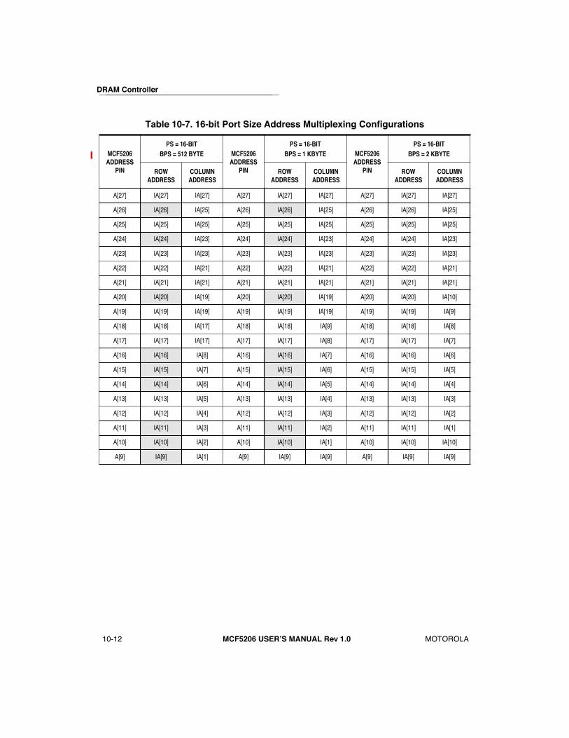
2
3
4
5
6
7
8
9
10
11
12
13
14
15
16
1
DRAM Controller
10-12
MCF5206 USERÕS MANUAL Rev 1.0
MOTOROLA
Table 10-7. 16-bit Port Size Address Multiplexing Configurations
MCF5206 ADDRESS
PIN
PS = 16-BITBPS = 512 BYTE MCF5206
ADDRESS PIN
PS = 16-BITBPS = 1 KBYTE MCF5206
ADDRESS PIN
PS = 16-BITBPS = 2 KBYTE
ROW ADDRESS
COLUMN ADDRESS
ROW ADDRESS
COLUMN ADDRESS
ROW ADDRESS
COLUMN ADDRESS
A[27] IA[27] IA[27] A[27] IA[27] IA[27] A[27] IA[27] IA[27]
A[26] IA[26] IA[25] A[26] IA[26] IA[25] A[26] IA[26] IA[25]
A[25] IA[25] IA[25] A[25] IA[25] IA[25] A[25] IA[25] IA[25]
A[24] IA[24] IA[23] A[24] IA[24] IA[23] A[24] IA[24] IA[23]
A[23] IA[23] IA[23] A[23] IA[23] IA[23] A[23] IA[23] IA[23]
A[22] IA[22] IA[21] A[22] IA[22] IA[21] A[22] IA[22] IA[21]
A[21] IA[21] IA[21] A[21] IA[21] IA[21] A[21] IA[21] IA[21]
A[20] IA[20] IA[19] A[20] IA[20] IA[19] A[20] IA[20] IA[10]
A[19] IA[19] IA[19] A[19] IA[19] IA[19] A[19] IA[19] IA[9]
A[18] IA[18] IA[17] A[18] IA[18] IA[9] A[18] IA[18] IA[8]
A[17] IA[17] IA[17] A[17] IA[17] IA[8] A[17] IA[17] IA[7]
A[16] IA[16] IA[8] A[16] IA[16] IA[7] A[16] IA[16] IA[6]
A[15] IA[15] IA[7] A[15] IA[15] IA[6] A[15] IA[15] IA[5]
A[14] IA[14] IA[6] A[14] IA[14] IA[5] A[14] IA[14] IA[4]
A[13] IA[13] IA[5] A[13] IA[13] IA[4] A[13] IA[13] IA[3]
A[12] IA[12] IA[4] A[12] IA[12] IA[3] A[12] IA[12] IA[2]
A[11] IA[11] IA[3] A[11] IA[11] IA[2] A[11] IA[11] IA[1]
A[10] IA[10] IA[2] A[10] IA[10] IA[1] A[10] IA[10] IA[10]
A[9] IA[9] IA[1] A[9] IA[9] IA[9] A[9] IA[9] IA[9]

DRAM Controller
MOTOROLA
MCF5206 USERÕS MANUAL Rev 1.0
10-13
2
3
4
5
6
7
8
9
10
11
12
13
14
15
16
1
The BPS field in each DCCR defines the DRAMC internal page size. The internal page size is used by the DRAMC to determine whether an transfer is a page hit or a page miss. The page size of the DRAM used in the bank is not always the same as the DRAMC internal page size. For example, if a 2 KByte page size is selected and an 8-bit wide DRAM is used, 11 address bits and 1 CAS signal are needed to define the page. However, if a 2 KByte page size is selected and a 32-bit wide DRAM is used, only 9 address signals and 4 CAS signals are needed to define the page. Using a DRAM which has a larger page size than is listed in the actual DRAM page size column of Table 10-9 for a given internal page size and port size gives no performance advantage.
To allow for future upgrades to larger DRAMs without requiring multiple printed circuit board layouts, the page size must remain constant. After the page size has been selected, use the tables to determine which address pins to use for the maximum DRAM size. These traces can then be routed to the DRAM socket on the printed circuit board.
Table 10-8. 32-bit Port Size Address Multiplexing Configurations
MCF5206 ADDRESS
PIN
PS = 32-BITBPS = 512 BYTE MCF5206
ADDRESS PIN
PS = 32-BITBPS = 1 KBYTE MCF5206
ADDRESS PIN
PS = 32-BITBPS = 2 KBYTE
ROW ADDRESS
CASROW
ADDRESSCAS
ROW ADDRESS
CAS
A[27] IA[27] IA[26] A[27] IA[27] IA[26] A[27] IA[27] IA[26]
A[26] IA[26] IA[26] A[26] IA[26] IA[26] A[26] IA[26] IA[26]
A[25] IA[25] IA[24] A[25] IA[25] IA[24] A[25] IA[25] IA[24]
A[24] IA[24] IA[24] A[24] IA[24] IA[24] A[24] IA[24] IA[24]
A[23] IA[23] IA[22] A[23] IA[23] IA[22] A[23] IA[23] IA[22]
A[22] IA[22] IA[22] A[22] IA[22] IA[22] A[22] IA[22] IA[22]
A[21] IA[21] IA[20] A[21] IA[21] IA[20] A[21] IA[21] IA[20]
A[20] IA[20] IA[20] A[20] IA[20] IA[20] A[20] IA[20] IA[20]
A[19] IA[19] IA[18] A[19] IA[19] IA[18] A[19] IA[19] IA[10]
A[18] IA[18] IA[18] A[18] IA[18] IA[18] A[18] IA[18] IA[9]
A[17] IA[17] IA[16] A[17] IA[17] IA[9] A[17] IA[17] IA[8]
A[16] IA[16] IA[16] A[16] IA[16] IA[8] A[16] IA[16] IA[7]
A[15] IA[15] IA[8] A[15] IA[15] IA[7] A[15] IA[15] IA[6]
A[14] IA[14] IA[7] A[14] IA[14] IA[6] A[14] IA[14] IA[5]
A[13] IA[13] IA[6] A[13] IA[13] IA[5] A[13] IA[13] IA[4]
A[12] IA[12] IA[5] A[12] IA[12] IA[4] A[12] IA[12] IA[3]
A[11] IA[11] IA[4] A[11] IA[11] IA[3] A[11] IA[11] IA[2]
A[10] IA[10] IA[3] A[10] IA[10] IA[2] A[10] IA[10] IA[10]
A[9] IA[9] IA[2] A[9] IA[9] IA[9] A[9] IA[9] IA[9]
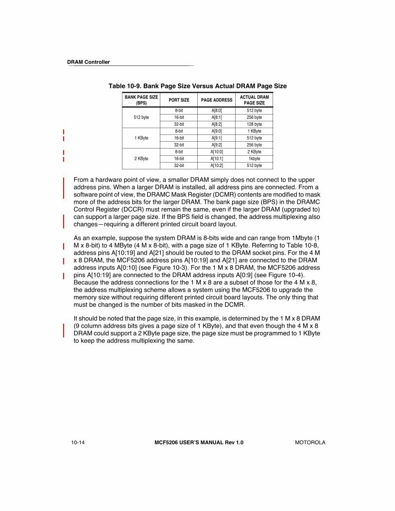
2
3
4
5
6
7
8
9
10
11
12
13
14
15
16
1
DRAM Controller
10-14
MCF5206 USERÕS MANUAL Rev 1.0
MOTOROLA
From a hardware point of view, a smaller DRAM simply does not connect to the upper address pins. When a larger DRAM is installed, all address pins are connected. From a software point of view, the DRAMC Mask Register (DCMR) contents are modified to mask more of the address bits for the larger DRAM. The bank page size (BPS) in the DRAMC Control Register (DCCR) must remain the same, even if the larger DRAM (upgraded to) can support a larger page size. If the BPS field is changed, the address multiplexing also changesÑrequiring a different printed circuit board layout.
As an example, suppose the system DRAM is 8-bits wide and can range from 1Mbyte (1 M x 8-bit) to 4 MByte (4 M x 8-bit), with a page size of 1 KByte. Referring to Table 10-8, address pins A[10:19] and A[21] should be routed to the DRAM socket pins. For the 4 M x 8 DRAM, the MCF5206 address pins A[10:19] and A[21] are connected to the DRAM address inputs A[0:10] (see Figure 10-3). For the 1 M x 8 DRAM, the MCF5206 address pins A[10:19] are connected to the DRAM address inputs A[0:9] (see Figure 10-4). Because the address connections for the 1 M x 8 are a subset of those for the 4 M x 8, the address multiplexing scheme allows a system using the MCF5206 to upgrade the memory size without requiring different printed circuit board layouts. The only thing that must be changed is the number of bits masked in the DCMR.
It should be noted that the page size, in this example, is determined by the 1 M x 8 DRAM (9 column address bits gives a page size of 1 KByte), and that even though the 4 M x 8 DRAM could support a 2 KByte page size, the page size must be programmed to 1 KByte to keep the address multiplexing the same.
Table 10-9. Bank Page Size Versus Actual DRAM Page Size
BANK PAGE SIZE (BPS)
PORT SIZE PAGE ADDRESSACTUAL DRAM
PAGE SIZE
512 byte8-bit A[8:0] 512 byte
16-bit A[8:1] 256 byte32-bit A[8:2] 128 byte
1 KByte 8-bit A[9:0] 1 KByte
16-bit A[9:1] 512 byte32-bit A[9:2] 256 byte
2 KByte8-bit A[10:0] 2 KByte
16-bit A[10:1] 1kbyte32-bit A[10:2] 512 byte

DRAM Controller
MOTOROLA
MCF5206 USERÕS MANUAL Rev 1.0
10-15
2
3
4
5
6
7
8
9
10
11
12
13
14
15
16
1
For the 4 M x 8 DRAM, the DCCR and DCMR would be programmed as follows:
DCCR: $57 (port size = 8-bit, page size = 1kbyte, burst page mode, read/write)DCMR: $001e0000 (A[20:17] are masked => 4 MByte)
Figure 10-3. Connection Diagram for 4Mbyte DRAM with 8-bit Port and 1Kbyte Page
For the 1 M x 8 DRAM, the DCCR and DCMR would be programmed as follows:
DCCR: $57 (port size = 8-bit, page size = 1kbyte, burst page mode, read/write)DCMR: $000e0000 (A[19:17] are masked => 1 MByte).
Figure 10-4. Connection Diagram for 1Mbyte DRAM with 8-Bit Port and 1Kbyte Page
10.3.3 Normal Mode Operation
Normal mode is the simplest form of DRAM transfer. In this mode, row addresses and column addresses are supplied for every transfer. For DRAM transfers initiated by the ColdFire core that access a bank programmed for normal mode, the MCF5206 supplies a row address on the address bus, drives DRAMW to indicate whether a read or a write
A[10]
A[9]
A[8]
A[7]
A[6]
A[5]
A[4]
A[3]
A[2]
A[1]
A[0]
RAS
CAS
WE
D[7:0]
A[21]
A[19]
A[18]
A[17]
A[16]
A[15]
A[14]
A[13]
A[12]
A[11]
A[10]
RAS[0]
CAS[0]
DRAMW
D[31:24]
4M x 8
DRAMMCF5206
A[9]
A[8]
A[7]
A[6]
A[5]
A[4]
A[3]
A[2]
A[1]
A[0]
RAS
CAS
WE
D[7:0]
A[19]
A[18]
A[17]
A[16]
A[15]
A[14]
A[13]
A[12]
A[11]
A[10]
RAS[0]
CAS[0]
DRAMW
D[31:24]
1M x 8
DRAMMCF5206
2
3
4
5
6
7
8
9
10
11
12
13
14
15
16
1
DRAM Controller
10-16
MCF5206 USERÕS MANUAL Rev 1.0
MOTOROLA
is occurring and asserts RAS. The MCF5206 then drives the column address onto the same address pins and asserts CAS. When the cycle is complete, both RAS and CAS are negated.
10.3.3.1 NONBURST TRANSFER IN NORMAL MODE.
A nonburst transfer to DRAM occurs when the operand size is the same or smaller than the DRAM port size (e.g.,longword transfer to a 32-bit port, or byte transfer to a 16-bit port). Nonburst transfers always start with the assertion of TS.
The start of a transfer to a DRAM bank can be delayed by the DRAMC until the programmed RAS precharge time is met. A transfer to a different DRAM bank than the previous transfer is never delayed due to RAS precharge since that bank has already been precharged.
The timing of nonburst reads and nonburst writes is identical in normal page mode, with the exception of when the DRAM drives data on reads and when the MCF5206 drives data on writes.
The fastest possible nonburst transfer in normal mode requires 3 clocks with a 1.5 clock RAS precharge time. You can program the DCTR to generate slower normal mode transfers.
Figure 10-6 shows the timing of a back-to-back nonburst byte-read transfer to an 8-bit port in normal mode.

DRAM Controller
MOTOROLA
MCF5206 USERÕS MANUAL Rev 1.0
10-17
2
3
4
5
6
7
8
9
10
11
12
13
14
15
16
1
.
Figure 10-5. Byte Read Transfers in Normal Mode with 8-bit DRAM
Clock H1
The first DRAM-read transfer starts in H1. During H1, the MCF5206 drives the row address on the A[27:9], drives DRAMW high indicating a DRAM-read transfer, drives SIZ[1:0] to $1 indicating a byte transfer, and asserts TS.
Clock L1
The MCF5206 asserts RAS to indicate the row address is valid on the address bus.
Clock H2
The MCF5206 negates TS, and drives the column address on the address bus.
Clock L2
The MCF5206 asserts CAS[0] to indicate the column address is valid on the address bus. At this point, the DRAM turns on its output drivers and begins driving data on D[31:24].
Clock H3
The internal transfer acknowledge asserts to indicate that the current transfer is completed and the data on the D[31:24] are registered on the next rising edge of CLK.
CLK
A[27:9]
RAS
CAS [0]
DRAMW
D[31:24]
TS
INTERNAL TA
ROW COL COLROW
H1 L1 H2 L2 H3 L3 H4 L4 H5 L5 H6 L6 H7 L7 H8 L8 H9

2
3
4
5
6
7
8
9
10
11
12
13
14
15
16
1DRAM Controller
10-18 MCF5206 USERÕS MANUAL Rev 1.0 MOTOROLA
Clock H4
The MCF5206 registers the read data driven by the DRAM and negates the internal transfer acknowledge, RAS and CAS[0], ending the first byte-read transfer. This begins the RAS precharge. Once CAS[0] is negated the DRAM disables its output drivers, and the data bus is three-stated.
Clock H6
Clock H6 is the earliest the next transfer initiated by the ColdFire core can start. The second DRAM byte-read transfer starts in H6. During H6, the MCF5206 drives the row address on the A[27:9], drives DRAMW high indicating a DRAM-read transfer, drives SIZ[1:0] to $1 indicating a byte transfer, and asserts TS.
Clock L6
Clock L6 is the same as Clock L1.
Clock H7
Clock H7 is the same as Clock H2.
Clock L7
Clock L7 is the same as Clock L2.
Clock H8
Clock H8 is the same as Clock H3.
Clock H9
Clock H9 is the same as Clock H4.
10.3.3.2 BURST TRANSFER IN NORMAL MODE. A burst transfer to DRAM is generated when the operand size is larger than the DRAM bank port size (e.g., line transfer to a 32-bit port, longword transfer to an 8-bit port). On all DRAM transfers, the MCF5206 asserts TS only once. The start of the secondary transfers of a burst is delayed by the DRAMC until the programmed RAS precharge time is reached.
The timing of burst reads and burst writes is identical in normal page mode, with the exception of when the DRAM drives data on reads and when the MCF5206 drives data on writes.
The fastest possible burst transfer in normal mode requires 3 clocks for the first transfer of the burst and 4 clocks for the secondary transfers (including a 1.5 clock RAS precharge time). You can program the DCTR to generate slower normal mode transfers.

DRAM Controller
MOTOROLA MCF5206 USERÕS MANUAL Rev 1.0 10-19
2
3
4
5
6
7
8
9
10
11
12
13
14
15
16
1Figure 10-6 shows the timing of a burst longword write transfer to a 16-bit port in normal mode.
Figure 10-6. Longword Write Transfer in Normal Mode with 16-bit DRAM
Clock H1
The first DRAM write transfer of the burst starts in H1. During H1, the MCF5206 drives the row address on A[27:9], drives DRAMW low indicating a DRAM write transfer, drives SIZ[1:0] to $0 indicating a longword transfer, and asserts TS. The address driven on the A[27:9] corresponds to the DRAM row address for the first transfer of the burst.
Clock L1
The MCF5206 asserts RAS to indicate the row address is valid on A[27:9].
Clock H2
The MCF5206 negates TS, drives the column address on A[27:9], and begins driving the data on D[31:16] for the first word write of the longword burst.
Clock L2
The MCF5206 asserts CAS[1:0] to indicate the column address is valid on the A[27:9].
CLK
A[27:9]
RAS
CAS [1:0]
DRAMW
D[31:16]
TS
INTERNAL TA
ROW COL COLROW
H1 L1 H2 L2 H3 L3 H4 L4 H5 L5 H6 L6 H7 L7 H8
2
3
4
5
6
7
8
9
10
11
12
13
14
15
16
1DRAM Controller
10-20 MCF5206 USERÕS MANUAL Rev 1.0 MOTOROLA
Clock H3
The internal transfer acknowledge asserts to indicate the first word transfer of the longword burst is completed on the next rising edge of CLK.
Clock H4
The MCF5206 negates the internal transfer acknowledge, RAS and CAS[1:0], ending the first word write transfer of the longword burst. This begins the RAS precharge. The MCF5206 drives the row address on A[27:9], and begins driving the data on D[31:16] for the second word write of the longword burst.
Clock L4/H5
The MCF5206 continues to negate RAS to meet the precharge time.
Clock L5
After the RAS precharge time is reached, the MCF5206 asserts RAS to indicate the row address is valid on A[27:9].
Clock H6
The MCF5206 drives the column address on A[27:9].
Clock L6
The MCF5206 asserts CAS[1:0] to indicate the column address is valid on A[27:9].
Clock H7
Clock H7 is the same as Clock H3.
Clock H8
The MCF5206 negates the internal transfer acknowledge, RAS and CAS[1:0], ending the second word write transfer of the longword burst. This begins the RAS precharge. When the burst write is completed, D[31:0] is three-stated.
10.3.4 Fast Page Mode OperationFast page mode operation allows faster successive transfers to locations in DRAM that have the same row address. All locations with the same row address are said to be on the same Òpage.Ó Successive transfers that have the same row address as the initial transfer are called Òpage hits,Ó while successive transfers with different row addresses are called Òpage misses.Ó
On the initial transfer to a page, the DRAMC stores the row address. The address of a successive transfer is compared with the stored row address to determine if the transfer

DRAM Controller
MOTOROLA MCF5206 USERÕS MANUAL Rev 1.0 10-21
2
3
4
5
6
7
8
9
10
11
12
13
14
15
16
1is a page hit or a page miss. For a page size of 512 byte (BPS=$0 in the DCTR), bits 31-9 of the transfer address must match the corresponding bits stored as the active row address to be a page hit. For a page size of 1 KByte (BPS=$1), bits 31-10 of the transfer address must match the corresponding bits of the active row address to be a page hit. For a page size of 2 KByte (BPS=$2), bits 31-11 of the transfer address must match the corresponding bits of the active row address to be a page hit.
Fast page-mode transfers are facilitated by having the RAS signal remain asserted while asserting CAS to access successive column locations determined by the column address. Once RAS asserts on a transfer to a page, the page is said to be ÒopenÓ and RAS remains asserted on all successive transfers to that page. If a transfer to a location in the current DRAM bank is a page hit, only the column address is driven and CAS is asserted.
In fast page mode, RAS is negate (precharge), ÒclosingÓ the current page, under the following conditions:
1. A transfer occurs to an address in the current DRAM bank that is a page miss
2. A transfer occurs to an address in the other DRAM bank
3. The MCF5206 loses bus mastership
4. A refresh cycle is pending
In each of these cases, the RAS negates and the DRAMC does not allow an access to that bank until the RAS precharge time is met.
10.3.4.1 BURST TRANSFER IN FAST PAGE MODE. A burst transfer to DRAM is generated when the operand size is larger than the DRAM bank port size (e.g., line transfer to a 32-bit port, longword transfer to an 8-bit port). Burst transfers can access from two to 16 segments of data in a single transfer. On all DRAM transfers the MCF5206 asserts TS only once. The internal TA is asserted to indicate the transfer of each segment of data. The start of the secondary transfers of a burst is delayed by the DRAMC until the programmed RAS precharge time is reached.
The timing of burst reads and burst writes is identical in fast page mode, with the exception of when the DRAM drives data on reads and when the MCF5206 drives data on writes.
The fastest possible burst transfer in normal mode takes 3 clocks for the initial transfer, 2 clocks for secondary transfers with a 0.5 clock CAS precharge time and a 1.5 clock RAS precharge time. You can program the DCTR to generate slower fast page mode transfers.

2
3
4
5
6
7
8
9
10
11
12
13
14
15
16
1DRAM Controller
10-22 MCF5206 USERÕS MANUAL Rev 1.0 MOTOROLA
Figure 10-7 shows the timing of a word write transfer to an 8-bit port in fast page mode.
Figure 10-7. Word Write Transfer in Fast Page Mode with 8-Bit DRAM
Clock H1
The first byte write transfer of the word burst starts in H1. During H1, the MCF5206 drives the row address on A[27:9], drives DRAMW low indicating a DRAM write transfer, drives SIZ[1:0] to $2 indicating a word transfer, and asserts TS. The address driven on A[27:9] corresponds to the row address for the first byte transfer of the burst.
Clock L1
The MCF5206 asserts RAS to indicate the row address is valid on A[27:9].
Clock H2
The MCF5206 negates TS, drives the column address on A[27:9], and begins driving the data on D[31:24].
Clock L2
The MCF5206 asserts CAS[0] to indicate the column address is valid on A[27:9].
CLK
A[27:9]
RAS
CAS [0]
DRAMW
D[31:24]
TS
INTERNAL TA
ROW COL COL
H1 L1 H2 L2 H3 L3 H4 L4 H5 L5 H6 L6

DRAM Controller
MOTOROLA MCF5206 USERÕS MANUAL Rev 1.0 10-23
2
3
4
5
6
7
8
9
10
11
12
13
14
15
16
1Clock H3
The internal transfer acknowledge asserts to indicate that the first byte transfer of the word burst is completed on the next rising edge of CLK.
Clock H4
The MCF5206 negates the internal transfer acknowledge, and CAS[0] ending the first byte write transfer of the word burst. At this point, the new page has been opened; therefore, the MCF5206 continues to assert RAS. The negation of CAS[0] begins the CAS precharge. The MCF5206 drives the next column address on A[27:9] and the next data is driven on D[31:24].
Clock L4
Clock L4 is the same as Clock L2.
Clock H5
Clock H5 is the same as Clock H3.
Clock H6
The MCF5206 negates the internal transfer acknowledge, and CAS[0] ending the final byte write of the word burst. Because the bank is in fast page mode, MCF5206 continues to assert RAS. The negation of CAS[0] begins the CAS precharge. When the burst write is completed, the MCF5206 three-states D[31:0].
10.3.4.2 PAGE HIT READ TRANSFER IN FAST PAGE MODE.
A read transfer to an open page results in a page-hit read. The timing of page-hit reads differs from the timing of page-hit writes (page-hit writes are described in Section 10.3.4.3 Page-Hit Write Transfer in Fast Page Mode). The start of a page-hit read transfer to a DRAM bank in fast page mode can be delayed by the DRAMC until the programmed CAS precharge time is reached.
The fastest possible nonburst page-hit read transfer in fast page mode takes 2 clocks with a 0.5 clock CAS precharge time. The fastest possible burst page-hit read transfer in fast page mode takes 2 clocks for the initial transfer, and 2 clocks for all secondary reads with a 0.5 clock CAS precharge time. You can program the DCTR to generate slower fast page mode transfers.
Figure 10-8 shows the timing of a nonburst read opening a page and a subsequent page-hit read being generated. The first transfer that opens the page is a longword read transfer from a 32-bit port in fast page mode. The first read transfer is followed by a second page-hit longword read transfer. The timing of a page-hit read transfer is the same regardless of whether the page was opened by a burst read, burst write, nonburst read, or nonburst write transfer.
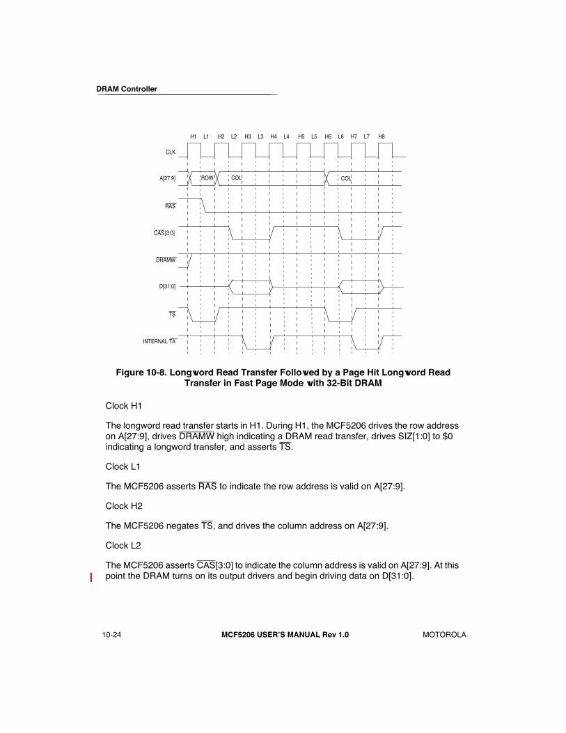
2
3
4
5
6
7
8
9
10
11
12
13
14
15
16
1DRAM Controller
10-24 MCF5206 USERÕS MANUAL Rev 1.0 MOTOROLA
Figure 10-8. Longword Read Transfer Followed by a Page Hit Longword Read Transfer in Fast Page Mode with 32-Bit DRAM
Clock H1
The longword read transfer starts in H1. During H1, the MCF5206 drives the row address on A[27:9], drives DRAMW high indicating a DRAM read transfer, drives SIZ[1:0] to $0 indicating a longword transfer, and asserts TS.
Clock L1
The MCF5206 asserts RAS to indicate the row address is valid on A[27:9].
Clock H2
The MCF5206 negates TS, and drives the column address on A[27:9].
Clock L2
The MCF5206 asserts CAS[3:0] to indicate the column address is valid on A[27:9]. At this point the DRAM turns on its output drivers and begin driving data on D[31:0].
CLK
A[27:9]
RAS
CAS [3:0]
DRAMW
D[31:0]
TS
INTERNAL TA
ROW COL COL
H1 L1 H2 L2 H3 L3 H4 L4 H5 L5 H6 L6 H7 L7 H8

DRAM Controller
MOTOROLA MCF5206 USERÕS MANUAL Rev 1.0 10-25
2
3
4
5
6
7
8
9
10
11
12
13
14
15
16
1Clock H3
The internal transfer acknowledge asserts to indicate that the longword read transfer is completed and that data on D[31:0] is registered on the next rising edge of CLK.
Clock H4
The MCF5206 negates the internal transfer acknowledge, and CAS[3:0], ending the longword read transfer. At this point the new page has been opened; therefore, the MCF5206 continues to assert RAS. Once CAS[3:0] are negated the DRAM disables its output drivers and the D[31:0] are three-stated. The negation of CAS[3:0] begins the CAS precharge.
Clock H6
Clock H6 is the earliest the next transfer initiated by the ColdFire core can start. In this case, a page-hit longword read is shown. The page-hit longword read transfer starts in H6. During H6, the MCF5206 drives the column address on A[27:9], drives DRAMW high indicating a DRAM read transfer, drives SIZ[1:0] to $0 indicating a longword transfer, and asserts TS.
Clock L6
The MCF5206 asserts CAS[3:0] to indicate the column address is valid on A[27:9]. At this point, the DRAM turns on its output drivers and begin driving data on D[31:0].
Clock H7
Clock H7 is the same as Clock H3.
Clock H8
The MCF5206 negates the internal transfer acknowledge, and CAS[3:0], ending the page-hit longword read transfer. Since the DRAM bank is in Fast Page Mode, the MCF5206 continues to assert RAS. Once CAS[3:0] are negated the DRAM disables itÕs output drivers and D[31:0] are three-stated. The negation of CAS[3:0] begins the CAS precharge.
10.3.4.3 PAGE-HIT WRITE TRANSFER IN FAST PAGE MODE. A write transfer to an open page results in a page-hit write. The timing of page-hit write transfers differs from the timing of page-hit read transfers. On a page-hit write transfer, CAS is asserted one cycle later than in a page-hit read transfer. This is because the write data is not driven until the cycle after TS is asserted and data must be set up prior to CAS assertion. The start of a page-hit write transfer to a DRAM bank in fast page mode can be delayed by the DRAMC until the programmed CAS precharge time is reached.
The fastest possible nonburst page-hit write transfer in fast page mode requires 3 clocks. The fastest possible burst page-hit write transfer in fast page mode requires 3 clocks for the initial transfer and 2 clocks for all secondary writes. You can program the DCTR to generate slower fast page mode transfers.
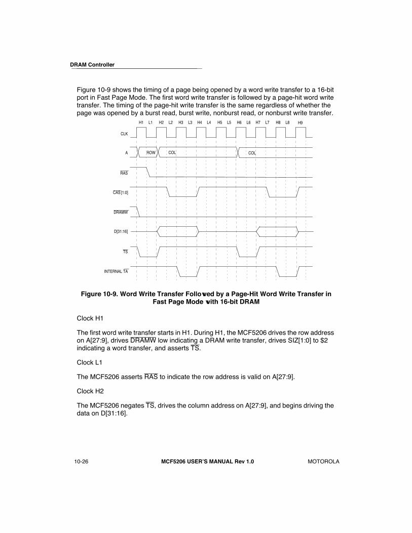
2
3
4
5
6
7
8
9
10
11
12
13
14
15
16
1DRAM Controller
10-26 MCF5206 USERÕS MANUAL Rev 1.0 MOTOROLA
Figure 10-9 shows the timing of a page being opened by a word write transfer to a 16-bit port in Fast Page Mode. The first word write transfer is followed by a page-hit word write transfer. The timing of the page-hit write transfer is the same regardless of whether the page was opened by a burst read, burst write, nonburst read, or nonburst write transfer.
Figure 10-9. Word Write Transfer Followed by a Page-Hit Word Write Transfer in Fast Page Mode with 16-bit DRAM
Clock H1
The first word write transfer starts in H1. During H1, the MCF5206 drives the row address on A[27:9], drives DRAMW low indicating a DRAM write transfer, drives SIZ[1:0] to $2 indicating a word transfer, and asserts TS.
Clock L1
The MCF5206 asserts RAS to indicate the row address is valid on A[27:9].
Clock H2
The MCF5206 negates TS, drives the column address on A[27:9], and begins driving the data on D[31:16].
CLK
A
RAS
CAS [1:0]
DRAMW
D[31:16]
TS
INTERNAL TA
ROW COL COL
H1 L1 H2 L2 H3 L3 H4 L4 H5 L5 H6 L6 H7 L7 H8 L8 H9

DRAM Controller
MOTOROLA MCF5206 USERÕS MANUAL Rev 1.0 10-27
2
3
4
5
6
7
8
9
10
11
12
13
14
15
16
1Clock L2
The MCF5206 asserts CAS[1:0] to indicate the column address is valid on A[27:9].
Clock H3
The internal transfer acknowledge asserts to indicate that the word write transfer is completed on the next rising edge of CLK.
Clock H4
The MCF5206 negates the internal transfer acknowledge, and CAS[1:0], ending the first word write transfer. At this point, the new page has been opened; therefore, the MCF5206 continues to assert RAS. The negation of CAS[1:0] begins the CAS precharge. When the write is completed, the MCF5206 three-states D[31:0].
Clock H6
Clock H6 is the earliest the next transfer initiated by the ColdFire core can start. In this case, a page-hit word write transfer is shown. The word write transfer starts in H6. During H6, the MCF5206 drives the column address on A[27:9], drives DRAMW low indicating a DRAM write transfer, drives SIZ[1:0] to $2 indicating a word transfer, and asserts TS.
Clock H7
Clock H7 is the same as Clock H2.
Clock L7
Clock L7 is the same as Clock L2.
Clock H8
Clock H8 is the same as Clock H3.
Clock H9
The MCF5206 negates the internal transfer acknowledge, and CAS[1:0], ending the second word write transfer. Because the DRAM bank is in fast page mode, the MCF5206 continues to assert RAS. The negation of CAS[1:0] begins the CAS precharge. When the write is completed, the MCF5206 three-states D[31:0].
10.3.4.4 PAGE MISS TRANSFER IN FAST PAGE MODE.
There is a potential performance penalty when using fast page mode. If a DRAM transfer misses the open page, the start of the transfer is delayed while RAS precharges. Therefore, fast page mode can increase performance when many successive transfers hit in the same page, but can also decrease performance when successive transfers hit in different pages.
2
3
4
5
6
7
8
9
10
11
12
13
14
15
16
1DRAM Controller
10-28 MCF5206 USERÕS MANUAL Rev 1.0 MOTOROLA
In cases where a page is open in one bank and a transfer hits in the other bank, the transfer is not delayed because the second bank has already been precharged.
The fastest possible page miss transfer in Fast page mode requires 4 clocks. The total number of clocks in a page miss transfer is the RAS precharge time, which causes the start of the transfer to be delayed (1 cycle for the fastest page miss transfer), plus the length of a fast page mode transfer to a new page (3 cycles for the fastest page miss transfer).
Figure 10-8 shows the timing of a page miss transfer in fast page mode. In this example, a page is opened by a byte read transfer to an 8-bit port. Then a second byte read transfer starts internally which misses the open page. Therefore, RAS must be precharged and a new page must be opened. The timing of the page-miss write transfer is the same as the timing of a page-miss read transfer.
Figure 10-10. Byte Read Transfer Followed by a Page-Miss Byte Read Transfer in Fast Page Mode with 8-Bit DRAM
CLK
A
RAS
CAS [0]
DRAMW
D[31:24]
TS
Internal TA
ROW COL COLROW
H9 L9 H10 L10 H11H1 L1 H2 L2 H3 L3 H4 L4 H5 L5 H6 L6 H7 L7 H8 L8

DRAM Controller
MOTOROLA MCF5206 USERÕS MANUAL Rev 1.0 10-29
2
3
4
5
6
7
8
9
10
11
12
13
14
15
16
1Clock H1
The first DRAM read transfer starts in H1. During H1, the MCF5206 drives the row address on A[27:9], drives DRAMW high indicating a DRAM read transfer, drives SIZ[1:0] to $1 indicating a byte transfer, and asserts TS.
Clock L1
The MCF5206 asserts RAS to indicate the row address is valid on A[27:9].
Clock H2
The MCF5206 negates TS, and drives the column address on A[27:9].
Clock L2
The MCF5206 asserts CAS[0] to indicate the column address is valid on A[27:9]. At this point the DRAM turns on its output drivers and begins driving data on D[31:24].
Clock H3
The internal transfer acknowledge asserts to indicate that the byte read transfer is completed and data on D[31:24] registered on the next rising edge of CLK.
Clock H4
The MCF5206 negates the internal transfer acknowledge, and CAS[0], ending the first byte read transfer. At this point, the new page has been opened; therefore, the MCF5206 continues to assert RAS. Once CAS[0] is negated, the DRAM disables its output drivers and D[31:0] is three-stated. The negation of CAS[0] begins the CAS precharge.
Clock H5/L5
A byte read transfer to the same DRAM bank is generated internally by the ColdFire core. This transfer misses the open page.
Clock H6
The ColdFire core initiated a DRAM transfer on the previous cycle that misses the open page. Therefore, the MCF5206 negates RAS, beginning the RAS precharge. Once the RAS precharge time has been reached, a transfer to a new page can start.
Clock H7
The byte read transfer to a new page starts in H7. During H7, the MCF5206 drives the row address on A[27:9], drives DRAMW high indicating a DRAM read transfer, drives SIZ[1:0] to $1 indicating a byte transfer, and asserts TS.
2
3
4
5
6
7
8
9
10
11
12
13
14
15
16
1DRAM Controller
10-30 MCF5206 USERÕS MANUAL Rev 1.0 MOTOROLA
Clock L7
The RAS precharge time has been met, so the MCF5206 asserts RAS is to indicate the row address is valid on A[27:9].
Clock H8
Clock H8 is the same as Clock H2.
Clock L8
Clock L8 is the same as Clock L2.
Clock H9
Clock H9 is the same as Clock H3.
Clock H10
Clock H10 is the same as Clock H4.
10.3.4.5 BUS ARBITRATION. If the MCF5206 loses bus mastership while a page is open (RAS is asserted), RAS is precharged. The RAS precharge timing depends on whether an active fast page mode DRAM transfer is in progress, whether a nonDRAM transfer is in progress, or whether the external bus is idle.
If the BL bit in the SIMR is cleared and BG is negated while an active fast page mode DRAM transfer is in progress, BD remains asserted until the transfer is complete. Once the DRAM transfer completes, the MCF5206 negates BD and begins precharging RAS.
In the case where the BL bit in the SIMR is cleared and BG is negated while a nonDRAM transfer is in progress and a page is open, the MCF5206 begins precharging RAS on the cycle following the negation of BG, even though BD remains asserted until the completion of the nonDRAM transfer.
If the BL bit in the SIMR is cleared and BG is negated while the external bus is idle and a page is open, the MCF5206 negates BD and begins precharging RAS on the cycle following the negation of BG.
When the BL bit in the SIMR is set to 1 and BG is asserted, the bus is locked with the MCF5206. If BG is negated while the bus is locked and a page is open, RAS and BD remains asserted, because the MCF5206 maintains bus mastership regardless of BG when the bus is locked.
NOTE
fast page mode is not supported for external master DRAMtransfers. A DRAM bank programmed for fast page mode,

DRAM Controller
MOTOROLA MCF5206 USERÕS MANUAL Rev 1.0 10-31
2
3
4
5
6
7
8
9
10
11
12
13
14
15
16
1operates in fast page mode for ColdFire core initiatedtransfers, but operates in burst page mode for external masterinitiated transfers.
Figure 10-11 shows the effect of bus arbitration on the DRAM signals when the external bus is idle and a page is open in fast page mode.
Figure 10-11. Bus Arbitration in Fast Page Mode
Clock H1
A Fast Page Mode transfer starts in H1. During H1, the MCF5206 drives the row address on A[27:9], and asserts TS.
Clock L1
The MCF5206 asserts RAS to indicate the row address is valid on A[27:9].
Clock H2
The MCF5206 negates TS, and drives the column address on A[27:9].
Clock L2
The MCF5206 asserts CAS to indicate the column address is valid on A[27:9].
CLK
A[27:9]
RAS
CAS
TS
INTERNAL TA
BG
BD
ROW COL
H1 L1 H2 L2 H3 L3 H4 L4 H5 L5 H6 L6 H7 L7

2
3
4
5
6
7
8
9
10
11
12
13
14
15
16
1DRAM Controller
10-32 MCF5206 USERÕS MANUAL Rev 1.0 MOTOROLA
Clock H3
The internal transfer acknowledge asserts to indicate that the current transfer is completed on the next rising edge of CLK.
Clock H4
The MCF5206 negates the internal transfer acknowledge, and CAS, ending the transfer. At this point, a page has been opened; therefore, the MCF5206 continues to assert RAS. The negation of CAS begins the CAS precharge.
Clock H6
After the bus has idled for two clocks, BG is negated (while the BL bit in the SIMR is cleared).
Clock H7
The MCF5206 then three-states the external bus signals, negates RAS (closing the page), and negates BD, relinquishing mastership of the bus. The negation of RAS begins the RAS precharge.
10.3.5 Burst Page-Mode OperationBurst page mode performs fast page mode transfers only for burst transfers. A burst transfer to DRAM occurs any time the operand size is larger than the DRAM bank port size (e.g., line transfer to a 32-bit port, longword transfer to an 8-bit port). After completing the burst, the MCF5206 negates RAS, closing the page. Because all secondary transfers of a burst are guaranteed to be page hits, a page miss never occurs in burst page mode. Nonburst transfers occur as in normal mode. Therefore, burst page mode always gives the same or better performance than normal mode.
The timing of read and write transfers is identical in burst page mode, with the exception of when the DRAM drives data on reads and when the MCF5206 drives data on writes.
The fastest possible burst transfer in burst page mode requires three clocks for the first transfer and two clocks on the secondary transfers. The fastest possible nonburst transfer in burst page mode requires three clocks. You can program the DCTR to generate slower burst page mode transfers.
Figure 10-12 shows a longword write transfer followed by a word read transfer to a 16-bit port with burst page mode enabled for the bank. The burst longword write transfer is handled as in fast page mode with the initial word transfer of the burst taking three cycles and the secondary word transfer taking two cycles. However, in burst page mode, the MCF5206 precharges RAS once the burst transfer is complete. The second transfer (a word read) is executed as in normal mode as it is not a burst transfer.

DRAM Controller
MOTOROLA MCF5206 USERÕS MANUAL Rev 1.0 10-33
2
3
4
5
6
7
8
9
10
11
12
13
14
15
16
1
Figure 10-12. Longword Write Transfer Followed by a Word Read Transfer in Burst Page Mode with 16-Bit DRAM
Clock H1
The first word write transfer of the longword burst starts in H1. During H1, the MCF5206 drives the row address on A[27:9], drives DRAMW low indicating a DRAM write transfer, drives SIZ[1:0] to $0 indicating a longword transfer, and asserts TS.
Clock L1
The MCF5206 asserts RAS to indicate the row address is valid on A[27:9].
Clock H2
The MCF5206 negates TS, drives the column address on A[27:9], and begins driving the data on D[31:16].
Clock L2
The MCF5206 asserts CAS[1:0] to indicate the column address is valid on A[27:9].
CLK
A[27:9]
RAS
CAS [1:0]
DRAMW
D[31:16]
TS
INTERNAL TA
ROW COL COL COLROW
H9 L9 H10 L10 H11H1 L1 H2 L2 H3 L3 H4 L4 H5 L5 H6 L6 H7 L7 H8 L8

2
3
4
5
6
7
8
9
10
11
12
13
14
15
16
1DRAM Controller
10-34 MCF5206 USERÕS MANUAL Rev 1.0 MOTOROLA
Clock H3
The internal transfer acknowledge asserts to indicate that the first word transfer of the longword burst is completed on the next rising edge of CLK.
Clock H4
The MCF5206 negates the internal transfer acknowledge, and CAS[1:0], ending the first word write transfer of the longword burst. At this point, the new page has been opened; therefore, the MCF5206 continues to assert RAS. The negation of CAS[1:0] begins the CAS precharge. The MCF5206 drives the next column address on A[27:9] and the next data on D[31:16].
Clock L4
Clock L4 is the same as Clock L2.
Clock H5
Clock H5 is the same as Clock H3.
Clock H6
The MCF5206 negates the internal transfer acknowledge, RAS, and CAS[1:0], ending the final write transfer of the longword burst. Because the bank is in burst page mode, MCF5206 precharges RAS at the end of the burst. The negation of RAS begins the RAS precharge. When the burst write is completed, the MCF5206 three-states D[31:0].
Clock H8
Clock H8 is the earliest the next transfer initiated by the ColdFire core can start. Because this next DRAM cycle is a nonburst word read transfer, it is handled as a normal mode transfer. During Clock H8, the MCF5206 drives the row address on A[27:9], drives DRAMW high indicating a DRAM read transfer, drives SIZ[1:0] to $2 indicating a word transfer, and asserts TS.
Clock L8
The MCF5206 asserts RAS to indicate the row address is valid on A[27:9].
Clock H9
The MCF5206 negates TS, and drives the column address on A[27:9]
Clock L9
The MCF5206 asserts CAS[1:0] to indicate the column address is valid on A[27:9]. At this point the DRAM turns on its output drivers and begins driving the data on D[31:16].
DRAM Controller
MOTOROLA MCF5206 USERÕS MANUAL Rev 1.0 10-35
2
3
4
5
6
7
8
9
10
11
12
13
14
15
16
1Clock H10
The internal transfer acknowledge asserts to indicate that the current transfer is completed and the data on D[31:16] registered on the next rising edge of CLK.
Clock H11
The MCF5206 registers the read data driven by the DRAM, and negates the internal transfer acknowledge, RAS and CAS[1:0], ending the word read transfer. This begins the RAS precharge. Once CAS is negated, the DRAM disables its output drivers and D[31:0] is three-stated.
10.3.6 Extended Data-Out (EDO) DRAM OperationExtended data-out (EDO) DRAMs do not three-state their output drivers at the negation of CAS on page read transfers as do fast-page-mode DRAMs. Instead, data remains valid until some time (typically 5 ns) after the next falling edge of CAS. This allows CAS to be precharged without the output data going invalid. The result is that a system using slower, less expensive EDO DRAM can achieve the same performance as a system using faster, more expensive fast-page-mode DRAMs.
The MCF5206 supports EDO DRAM with a CAS timing that takes advantage of the read data remaining valid after CAS negates. To enable the EDO CAS timing for both DRAM banks, set the EDO Enable bit in the DCTR to 1. When set to 1, CAS negates one-half clock cycle earlier for fast-page-mode and burst-page-mode transfers than when the EDO Enable bit is cleared. At higher clock frequencies, the EDO CAS timing allows slower, less expensive EDO DRAMs to be used, since the CAS precharge starts before data is registered on read transfers. For the fastest timing in fast page mode or burst page mode, having the EDO Enable bit set gives one clock of CAS precharge time, rather than one-half of a clock with the EDO Enable bit cleared.
Since EDO DRAM continues to drive data after a read as long as RAS is asserted, be careful with the system design using EDO DRAM to ensure bus contention does not occur when a nonDRAM transfer occurs while a page is open in fast page mode.
NOTE
Failure to use normal mode or burst page mode with EDODRAM without external circuitry to control the DRAM outputdrivers could result in damage to the MCF5206 and thesystem.
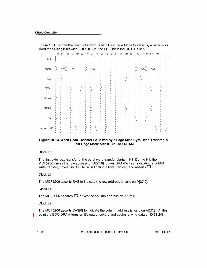
2
3
4
5
6
7
8
9
10
11
12
13
14
15
16
1DRAM Controller
10-36 MCF5206 USERÕS MANUAL Rev 1.0 MOTOROLA
Figure 10-13 shows the timing of a word read in Fast Page Mode followed by a page miss word read using 8-bit wide EDO DRAM (the EDO bit in the DCTR is set).
Figure 10-13. Word Read Transfer Followed by a Page Miss Byte Read Transfer in Fast Page Mode with 8-Bit EDO DRAM
Clock H1
The first byte read transfer of the burst word transfer starts in H1. During H1, the MCF5206 drives the row address on A[27:9], drives DRAMW high indicating a DRAM write transfer, drives SIZ[1:0] to $2 indicating a byte transfer, and asserts TS.
Clock L1
The MCF5206 asserts RAS to indicate the row address is valid on A[27:9].
Clock H2
The MCF5206 negates TS, drives the column address on A[27:9].
Clock L2
The MCF5206 asserts CAS[0] to indicate the column address is valid on A[27:9]. At this point the EDO DRAM turns on itÕs output drivers and begins driving data on D[31:24].
CLK
A[27:9]
RAS
CAS [0]
DRAMW
D[31:24]
TS
INTERNAL TA
ROW COL COL ROW COL
H9 L9 H10 L10 H11H1 L1 H2 L2 H3 L3 H4 L4 H5 L5 H6 L6 H7 L7 H8 L8 L11
DRAM Controller
MOTOROLA MCF5206 USERÕS MANUAL Rev 1.0 10-37
2
3
4
5
6
7
8
9
10
11
12
13
14
15
16
1Clock H3
The internal transfer acknowledge asserts to indicate that the first byte read transfer of the word burst is completed and the data on D[31:24] registered on the next rising edge of CLK.
Clock L3
With EDO DRAM, data is driven continuously on a read after the falling edge of CAS until the next falling edge of CAS or until the rising edge of RAS. This allows the MCF5206 to negate CAS[0] on L3 to allow more CAS precharge time. The negation of CAS[0] begins the CAS precharge.
Clock H4
The MCF5206 negates the internal transfer acknowledge, ending the first byte read transfer of the word burst. At this point, the new page has been opened; therefore, the MCF5206 continues to assert RAS. The MCF5206 drives the next column address on A[27:9].
Clock L4
The MCF5206 asserts CAS[0] to indicate the column address is valid on A[27:9]. At this point, the EDO DRAM begins driving the data on D[31:24].
Clock H5
Clock H5 is the same as Clock H3.
Clock L5
Clock L5 is the same as Clock L3.
Clock H6
The MCF5206 negates the internal transfer acknowledge, ending the final byte read transfer of the word burst. Because the bank is in fast page mode, MCF5206 continues to assert RAS. Because RAS remains asserted, the EDO DRAM continues to drive the data from the previous read transfer on D[31:24].
Clock H7/L7
A byte read transfer to the same DRAM bank is generated internally by the ColdFire core. This transfer misses the open page.
Clock H8
The ColdFire core initiated a DRAM transfer on the previous cycle that missed the open page. Therefore, the MCF5206 negates RAS, beginning the RAS precharge. Once the

2
3
4
5
6
7
8
9
10
11
12
13
14
15
16
1DRAM Controller
10-38 MCF5206 USERÕS MANUAL Rev 1.0 MOTOROLA
RAS precharge time has been reached, a transfer to a new page can start. Once RAS is negated, the EDO DRAM disables its output drivers and D[31:0] is three-stated.
Clock H9
The byte read transfer to a new page starts in H9. During H9, the MCF5206 drives the row address on A[27:9], drives DRAMW high indicating a DRAM read transfer, drives SIZ[1:0] to $1 indicating a byte transfer, and asserts TS.
Clock L9
Now that the RAS precharge time has been reached, the MCF5206 asserts RAS is to indicate the row address is valid on A[27:9].
Clock H10
Clock H10 is the same as Clock H2.
Clock L10
Clock L10 is the same as Clock L2.
Clock H11
Clock H11 is the same as Clock H3.
Clock H12
The MCF5206 negates the internal transfer acknowledge, ending the byte-read transfer. Because the bank is in fast page mode, MCF5206 continues to assert RAS. Because RAS remains asserted, the EDO DRAM continues to drive the data from the previous read transfer on D[31:24].
10.3.7 Refresh OperationThe DRAMC supports CAS-before-RAS refresh. Refresh cycles can be generated while nonDRAM transfers are actively using the external bus. Only transfers accessing the DRAM banks delay a refresh cycle. Both DRAM banks are refreshed on each refresh cycle.
The value stored in the RC field of the DCRR determines the rate at which the refresh controller internally requests refreshes in the DRAMC. The DRAMC does not immediately initiate a refresh cycle if a DRAM transfer is occurring when the internal refresh request is made. The DRAMC waits until the active DRAM transfer is complete and then initiates the DRAM refresh cycle. Refresh cycles occur immediately after the internal refresh request is made during idle bus cycles and during nonDRAM transfers.
DRAM Controller
MOTOROLA MCF5206 USERÕS MANUAL Rev 1.0 10-39
2
3
4
5
6
7
8
9
10
11
12
13
14
15
16
1NOTE
Add margin when determining the value to program into theRC field of the DCRR so that a refresh cycle delayed by thelongest possible DRAM transfer does not violate the refreshrate specified for the DRAMs being used.
Programming the RC field in the DCRR to $000 causes internal refresh requests to occur at the slowest rateÑonce every 65,536 system clock cycles. Programming the RC field in the DCRR to $001 causes internal refresh requests to occur at the fastest rateÑonce every 16 system clocks. If multiple refresh requests occur while waiting for a DRAM transfer to finish, only one refresh cycle is generated.
Writing to the DCRR causes an internal refresh request to occur and the refresh counter to be reloaded. If the DCRR is written while a refresh request is pending, only one refresh cycle is generated. If the DCRR is written while a refresh cycle is in progress, another refresh cycle is not generated after the one in progress completes.
The refresh period is the amount of time between internal refresh requests. The refresh period can be calculated from the value programmed in the RC field of the DCRR using the following equations:
For RC>$000:
Refresh period = RC x16 x (1/system clock frequency)
For RC=$000:
Refresh period = 65536 x (1/system clock frequency)
When the DRAMC initiates a refresh cycle, it delays any DRAM transfer initiated by the ColdFire core or by an external master until the RAS precharge is complete at the end of refresh cycle. If a DRAM transfer is initiated by the ColdFire core while a refresh cycle is in progress and the MCF5206 is not the bus master, bus request (BR) is not asserted until after the refresh completes.
A master reset terminates any active refresh cycle and resets the refresh controller. Master reset is required on all power-on resets. During a master reset, refresh cycles do not occur; after a master reset, refreshes occur at the slowest rate (DCRR is initialized to $0000).
NOTE
During a master reset, the DCCR is reset to $000 (giving theslowest refresh rate) and the DCTR is reset to $0000 (givingthe fastest waveform timing). After a master reset, theinitialization sequence should program the DRAMC RefreshRegister (DCRR) and the DRAMC Timing Register (DCTR)
2
3
4
5
6
7
8
9
10
11
12
13
14
15
16
1DRAM Controller
10-40 MCF5206 USERÕS MANUAL Rev 1.0 MOTOROLA
such that refresh cycles are generated at the required rate andwith the required timing for the DRAM in the system. Ingeneral, DRAMs require an initial pause after power-up andrequire a minimum number of DRAM cycles to be run beforethe DRAM is ready for use. This initialization sequence mustbe handled through software.
Normal reset does not affect a refresh cycle in progress and does not reset the refresh controller. Refreshes occur during a normal reset with the timing specified in the DCTR and at the rate specified in the DCRR.
10.3.8 External Master Use of the DRAM ControllerThe DRAMC can support external master-initiated transfers. When an external master is the bus master, the MCF5206 registers all available address signals, R/W, and SIZ[1:0] on the rising edge of clock when TS is asserted. Based on the address, direction, and data size, the DRAMC asserts RAS, CAS, DRAMW, and conditionally drive the address bus.
NOTE
If you do not want the MCF5206 DRAMC to respond onexternal master transfers, TS should not be asserted to theMCF5206 during external master transfers. The MCF5206,however, continues to generate DRAM refresh cycles whilethe bus is granted to an external master.
NOTE
The driving of the data on writes and the latching of data onreads based on the data size and port size of the DRAM is theresponsibility of the external master. The MCF5206 does notdrive the data bus when it is not master of the external bus.
The MCF5206 can delay the access to DRAM for an external master initiated transfer if a refresh request is pending or if the programmed RAS precharge time has not been reached. If there is a refresh cycle in progress or if there is a refresh request pending when an external master starts a DRAM transfer, the MCF5206 does not start driving the row address and assert RAS until the RAS precharge time has been reached after completing the refresh cycle. If a refresh request occurs during an external master DRAM transfer, the refresh cycle is delayed until the external master DRAM transfer is completed. If the programmed RAS precharge time from the previous DRAM transfer has not been reached, the MCF5206 does not start driving the row address and assert RAS until the precharge time has been reached.
For external master DRAM transfers, the MCF5206 drives TA as an output. TA is asserted to signify the end of each transfer (or subtransfer in the case of a burst). The assertion of TA can be used for latching data on read transfers and can also be used by the external master to trigger the driving of new write data for successive transfers during bursts.
DRAM Controller
MOTOROLA MCF5206 USERÕS MANUAL Rev 1.0 10-41
2
3
4
5
6
7
8
9
10
11
12
13
14
15
16
1When using the MCF5206 to multiplex the address for external master DRAM transfers (DAEM bit in the DCTR is set), the external master must stop driving the address bus during the clock cycle after TS is asserted. This allows the MCF5206 to drive the row address and the column address on A[27:9] at the appropriate times. If the external master cannot three-state the address bus, the driving of the address by the MCF5206 should be disabled and the address multiplexing for external master transfers must be handled in the external system.
If address multiplexing for external master transfers is to be handled in the external system, the DRAMC must be configured to three-state the address bus during these transfers by clearing the DAEM bit in the DCTR. This does not affect the operation of TA, RAS, CAS, or DRAMW during external master DRAM transfers.
NOTE
The MCF5206 does not drive the address for external masterchip select or default memory transfers.
10.3.8.1 EXTERNAL MASTER NONBURST TRANSFER IN NORMAL MODE. An external master nonburst transfer to DRAM is generated when the operand size is the same or smaller than the DRAM port size (e.g., longword transfer to a 32-bit port or byte transfer to a 16-bit port). The external master must assert TS at the start of all non-burst transfers.
The timing of nonburst reads and nonburst writes is identical in normal page mode, with the exception of when the DRAM drives data on reads and when the external master drives data on writes.
The fastest possible nonburst transfer in normal mode requires 5 clocks. You can program the DCTR to generate slower normal mode transfers.

2
3
4
5
6
7
8
9
10
11
12
13
14
15
16
1DRAM Controller
10-42 MCF5206 USERÕS MANUAL Rev 1.0 MOTOROLA
Figure 10-14 illustrates the timing of an external master DRAM byte read transfer followed by a byte write transfer to a 8-bit port in normal mode.
Figure 10-14. External Master Byte Read Transfer Followed by Byte Write Transfer in Normal Mode with 16-Bit DRAM
Clock H1/L1
An external master is the current bus master. The external master starts a DRAM transfer by driving A[27:0], driving R/W high indicating a read transfer, driving SIZ[1:0] to $1 indicating a byte transfer, and asserting TS. These inputs to the MCF5206 must be set up with respect to the rising edge of CLK H2.
Clock H2
On the rising edge of CLK when TS is asserted, the MCF5206 registers the address and attribute signals. The MCF5206 internally decodes these signals and determine if the external master transfer is a DRAM access. The external master negates TS and must three-state A[27:0] after the rising edge of CLK H2, if the internal address multiplexing is to be used.
CLK
A[27:0]
RAS
CAS [0]
DRAMW
D[31:24]
TS
TA
COLA COLAROWAROWA
H9 L9 H10 L10 H11H1 L1 H2 L2 H3 L3 H4 L4 H5 L5 H6 L6 H7 L7 H8 L8 L11
R/W
SIZ[1:0] $1 $1
DRAM Controller
MOTOROLA MCF5206 USERÕS MANUAL Rev 1.0 10-43
2
3
4
5
6
7
8
9
10
11
12
13
14
15
16
1Clock H3
The MCF5206 has determined that the external master transfer is a DRAM access, so the MCF5206 drives A[27:0] with the same value as was registered on the rising edge of H2. A[27:9] is the DRAM row address. The MCF5206 also drives DRAMW high, indicating a DRAM read cycle.
Clock L3
The MCF5206 asserts RAS to indicate the row address is valid on A[27:9].
Clock H4
The MCF5206 internally multiplexes the address and drives out the column address on A[27:9]. The MCF5206 also actively drives TA negated.
Clock L4
The MCF5206 asserts CAS[0] to indicate the column address is valid on A[27:9]. At this point the DRAM turns on its output drivers and begin driving the data on D[31:24].
Clock H5
The MCF5206 asserts the TA signal to indicate that the byte read transfer is completed and the read data valid on D[31:24] on the next rising edge of CLK.
Clock H6
The MCF5206 then negates RAS, CAS[0], and TA and three-states A[27:0], ending the byte-read transfer. The negation of RAS starts the RAS precharge. Once A[27:0] has three-stated, the external master can start another transfer. In this case, the external master starts a DRAM byte write transfer immediately by driving A[27:0], driving R/W low indicating a write transfer, driving SIZ[1:0] to $1 indicating a byte transfer, and asserting TS. The external master must drive the data in the correct byte lanes based on the data size and the port size of the DRAM, and must drive the data to meet the timing specifications of the DRAM. In this case, the external master should drive the write data on D[31:24].
Clock H7
The MCF5206 three-states TA. On the rising edge of CLK where TS is asserted, the MCF5206 registers the address and attribute signals. The MCF5206 internally decodes these signals and determine if the external master transfer is a DRAM access. The external master must three-state A[27:0] after the rising edge of CLK H2, if the internal address multiplexing is to be used.
2
3
4
5
6
7
8
9
10
11
12
13
14
15
16
1DRAM Controller
10-44 MCF5206 USERÕS MANUAL Rev 1.0 MOTOROLA
Clock H8
The MCF5206 has determined that the external master transfer is a DRAM access, so the MCF5206 drives the A[27:0] with the same value as was registered on the rising edge of H2. A[27:9] is the row address for the DRAM. The MCF5206 also drives DRAMW low, indicating a DRAM write cycle.
Clock L8
Clock L8 is the same as Clock L3.
Clock H9
Clock H9 is the same as Clock H4.
Clock L9
The MCF5206 asserts CAS[0] to indicate the column address is valid on A[27:9]. The external master must set up and hold the data with respect to the falling edge of CAS[0] based on the DRAM specifications.
Clock H10
The MCF5206 asserts the TA signal to indicate that the byte write transfer is completed on the next rising edge of CLK.
Clock H11
The MCF5206 then negates RAS, CAS[0], and TA, and three-state the address bus, ending the byte write transfer. The negation of RAS starts the RAS precharge. Once A[27:0] has three-stated, the external master can start another transfer.
Clock H12
The MCF5206 three-states TA.
10.3.8.2 EXTERNAL MASTER BURST TRANSFER IN NORMAL MODE. A burst transfer to DRAM is generated when the operand size is larger than the DRAM bank port size (e.g., line transfer to a 32-bit port, longword transfer to an 8-bit port). On DRAM burst transfers, the external master should assert TS only once. The start of the secondary transfers of a burst is delayed by the DRAMC until the programmed RAS precharge time is met.
The timing of external master burst reads and burst writes is identical in normal page mode, with the exception of when the DRAM drives data on reads and when the external master drives data on writes.
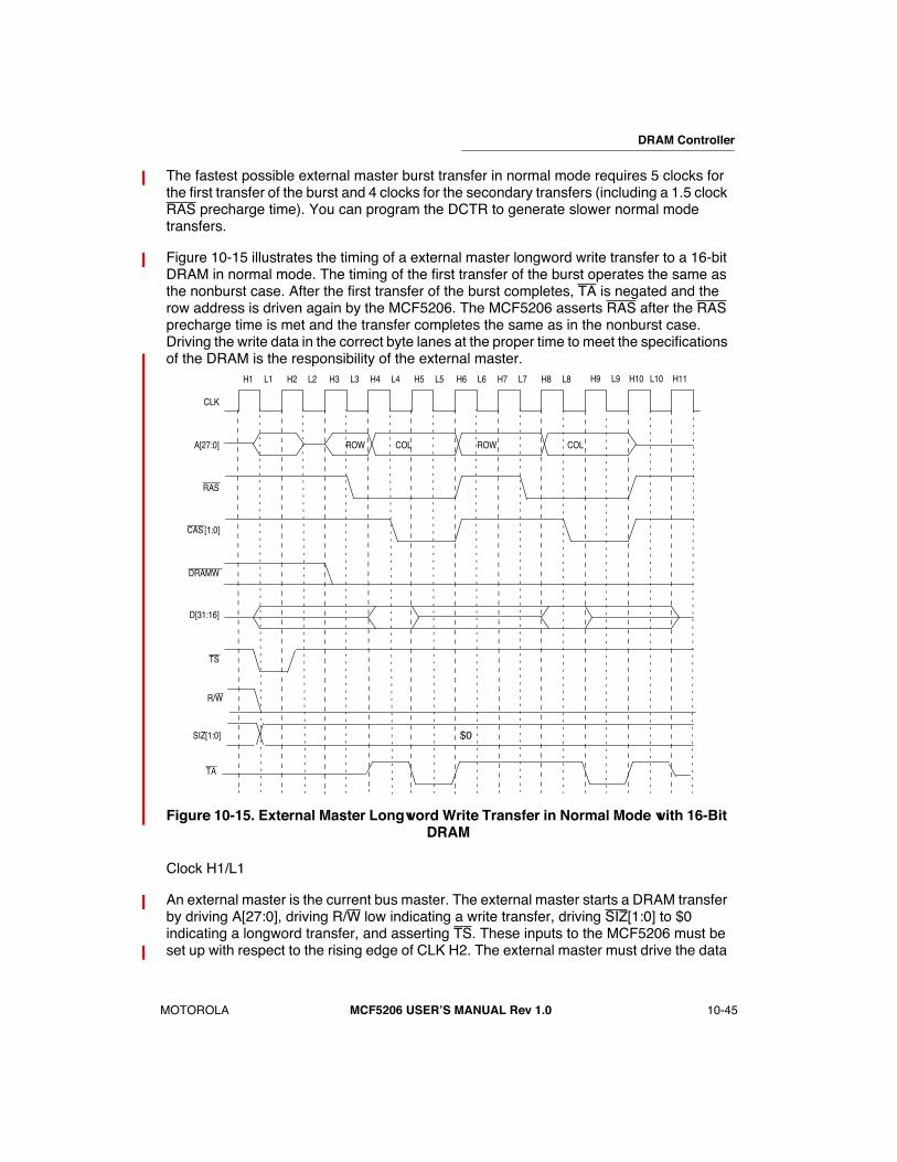
DRAM Controller
MOTOROLA MCF5206 USERÕS MANUAL Rev 1.0 10-45
2
3
4
5
6
7
8
9
10
11
12
13
14
15
16
1The fastest possible external master burst transfer in normal mode requires 5 clocks for the first transfer of the burst and 4 clocks for the secondary transfers (including a 1.5 clock RAS precharge time). You can program the DCTR to generate slower normal mode transfers.
Figure 10-15 illustrates the timing of a external master longword write transfer to a 16-bit DRAM in normal mode. The timing of the first transfer of the burst operates the same as the nonburst case. After the first transfer of the burst completes, TA is negated and the row address is driven again by the MCF5206. The MCF5206 asserts RAS after the RAS precharge time is met and the transfer completes the same as in the nonburst case. Driving the write data in the correct byte lanes at the proper time to meet the specifications of the DRAM is the responsibility of the external master.
Figure 10-15. External Master Longword Write Transfer in Normal Mode with 16-Bit DRAM
Clock H1/L1
An external master is the current bus master. The external master starts a DRAM transfer by driving A[27:0], driving R/W low indicating a write transfer, driving SIZ[1:0] to $0 indicating a longword transfer, and asserting TS. These inputs to the MCF5206 must be set up with respect to the rising edge of CLK H2. The external master must drive the data
CLK
A[27:0]
RAS
CAS [1:0]
DRAMW
D[31:16]
TS
TA
COL COLROWROW
H9 L9 H10 L10 H11H1 L1 H2 L2 H3 L3 H4 L4 H5 L5 H6 L6 H7 L7 H8 L8
R/W
SIZ[1:0] $0
2
3
4
5
6
7
8
9
10
11
12
13
14
15
16
1DRAM Controller
10-46 MCF5206 USERÕS MANUAL Rev 1.0 MOTOROLA
in the correct byte lanes based on the data size and the port size of the DRAM, and must drive the data to meet the timing specifications of the DRAM. In this case, the external master should drive the write data on D[31:16].
Clock H2
On the rising edge of CLK when TS is asserted, the MCF5206 registers the address and attribute signals. It internally decodes these signals and determine if the external master transfer is a DRAM access. The external master negates TS and must three-state A[27:0] after the rising edge of CLK H2, if the internal address multiplexing is to be used.
Clock H3
The MCF5206 has determined that the external master transfer is a DRAM access, so the MCF5206 drives A[27:0] with the same value as was registered on the rising edge of H2. A[27:9] is the DRAM row address. The MCF5206 also drives DRAMW low indicating a DRAM write cycle.
Clock L3
The MCF5206 asserts RAS to indicate the row address is valid on A[27:9].
Clock H4
The MCF5206 internally multiplexes the address and drives out the column address on A[27:9]. The MCF5206 also actively drives TA negated.
Clock L4
The MCF5206 asserts CAS[1:0] to indicate the column address is valid on A[27:9]. The external master must set up and hold the first word of data on D[31:16] with respect to the falling edge of CAS[1:0] based on the DRAM specifications.
Clock H5
The MCF5206 asserts the TA signal to indicate that the first word write transfer of the longword burst is completed on the next rising edge of CLK.
Clock H6
The MCF5206 negates RAS, CAS[1:0], and TA, ending the first word transfer of the longword burst. The negation of RAS starts the RAS precharge. The MCF5206 drives the row address again for second word transfer of the longword burst write.
Clock L7
Once the RAS precharge time has been met, the MCF5206 asserts RAS to indicate the row address is valid on A[27:9].
DRAM Controller
MOTOROLA MCF5206 USERÕS MANUAL Rev 1.0 10-47
2
3
4
5
6
7
8
9
10
11
12
13
14
15
16
1Clock H8
The MCF5206 internally increments and multiplexes the address and drives out the column address on A[27:9] for the second word transfer of the longword burst write.
Clock L8
Clock L8 is the same as Clock L4. The MCF5206 asserts CAS[1:0] to indicate the column address is valid on A[27:9]. The external master must set up and hold the second word of data on D[31:16] with respect to the falling edge of CAS[1:0] based on the DRAM specifications.
Clock H9
Clock H9 is the same as Clock H5. The MCF5206 asserts the TA signal to indicate that the second word write transfer of the longword burst is completed on the next rising edge of CLK.
Clock H10
The MCF5206 negates RAS, CAS[1:0], and TA, and three-states A[27:0], ending the second word transfer of the longword burst. The negation of RAS starts the RAS precharge. Once A[27:0] has three-stated, the external master can start another transfer.
Clock H11
The MCF5206 three-states TA.
10.3.8.3 EXTERNAL MASTER BURST TRANSFER IN BURST PAGE MODE. Burst page mode does fast page mode transfers only for burst transfers. A burst transfer to DRAM is generated any time the operand size is larger than the DRAM bank port size (e.g., line transfer to a 32-bit port, longword transfer to an 8-bit port). After completing the burst transfer, the MCF5206 negates RAS, closing the page. Because all secondary transfers of a burst are guaranteed to be page hits, a page miss never occurs in burst page mode. Nonburst transfers occur as in normal mode (for nonburst transfers in burst page mode, refer to Section 10.3.8.1 External Master NonBurst Transfer in Normal Mode). Therefore, burst page mode always gives the same or better performance than normal mode.
Because the DRAMC does not support fast page mode for external master transfers, a DRAM bank programmed for either burst page mode or fast page mode operates as burst page mode.
The timing of read transfers and write transfers is identical in burst page mode, with the exception of when the DRAM drives data on reads and when the external master drives data on writes.
The fastest possible external master burst transfer in burst page mode requires 5 clocks for the first transfer of the burst and two clocks for the secondary transfers. The fastest
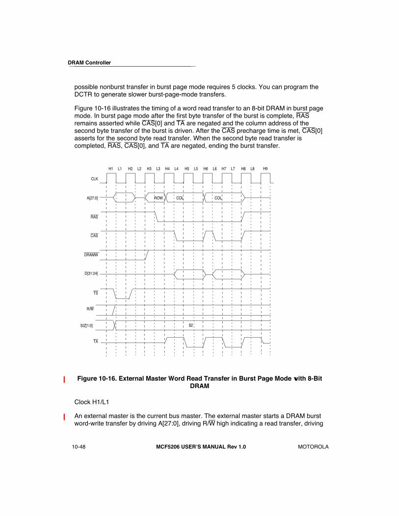
2
3
4
5
6
7
8
9
10
11
12
13
14
15
16
1DRAM Controller
10-48 MCF5206 USERÕS MANUAL Rev 1.0 MOTOROLA
possible nonburst transfer in burst page mode requires 5 clocks. You can program the DCTR to generate slower burst-page-mode transfers.
Figure 10-16 illustrates the timing of a word read transfer to an 8-bit DRAM in burst page mode. In burst page mode after the first byte transfer of the burst is complete, RAS remains asserted while CAS[0] and TA are negated and the column address of the second byte transfer of the burst is driven. After the CAS precharge time is met, CAS[0] asserts for the second byte read transfer. When the second byte read transfer is completed, RAS, CAS[0], and TA are negated, ending the burst transfer.
Figure 10-16. External Master Word Read Transfer in Burst Page Mode with 8-Bit DRAM
Clock H1/L1
An external master is the current bus master. The external master starts a DRAM burst word-write transfer by driving A[27:0], driving R/W high indicating a read transfer, driving
CLK
A[27:0]
RAS
CAS
DRAMW
D[31:24]
TS
TA
COL COLROW
H9H1 L1 H2 L2 H3 L3 H4 L4 H5 L5 H6 L6 H7 L7 H8 L8
R/W
SIZ[1:0] $2

DRAM Controller
MOTOROLA MCF5206 USERÕS MANUAL Rev 1.0 10-49
2
3
4
5
6
7
8
9
10
11
12
13
14
15
16
1SIZ[1:0] to $2 indicating a word transfer, and asserting TS. These inputs to the MCF5206 must be set up with respect to the rising edge of CLK H2.
Clock H2
On the rising edge of CLK when TS is asserted, the MCF5206 registers the address and attribute signals. It internally decodes these signals and determine if the external master transfer is a DRAM access. The external master negates TS and must three-state A[27:0] after the rising edge of CLK H2, if the internal address multiplexing is to be used.
Clock H3
The MCF5206 has determined that the external master transfer is a DRAM access, so the MCF5206 drives A[27:0] with the same value as was registered on the rising edge of H2. A[27:9] is the DRAM row address. The MCF5206 also drives DRAMW high indicating a DRAM read cycle.
Clock L3
The MCF5206 asserts RAS to indicate the row address is valid on A[27:9].
Clock H4
The MCF5206 internally multiplexes the address and drives out the column address on A[27:9]. The MCF5206 also actively drives TA negated.
Clock L4
The MCF5206 asserts CAS[0] to indicate the column address is valid on A[27:9]. At this point the DRAM turns on itÕs output drivers and begin driving the data on D[31:24].
Clock H5
The MCF5206 asserts the TA signal to indicate that the first byte read transfer of the burst is completed and the read data is valid on D[31:24] on the next rising edge of CLK.
Clock H6
The MCF5206 negates CAS[0], and TA, ending the first byte read transfer of the burst. Because the bank is in burst page mode, the MCF5206 continues to assert RAS. The negation of CAS[0] starts the CAS precharge. The MCF5206 drives the column address on A[27:9] for second byte read transfer of the burst.
Clock L6
After the CAS precharge time is met, the MCF5206 asserts CAS[0] to indicate the column address is valid on A[27:9]. At this point the DRAM turns on its output drivers and begins driving the data bus.
2
3
4
5
6
7
8
9
10
11
12
13
14
15
16
1DRAM Controller
10-50 MCF5206 USERÕS MANUAL Rev 1.0 MOTOROLA
Clock H7
Clock H7 is the same as Clock H5.
Clock H8
The MCF5206 negates RAS, CAS[0], and TA, and three-states A[27:0], ending the final byte read transfer of the burst. Because the bank is in burst page mode, MCF5206 negates RAS when the burst transfer is completed. The negation of RAS starts the RAS precharge. Once A[27:0] has three-stated, the external master can start another transfer.
Clock H9
The MCF5206 three-states TA.
10.3.8.4 LIMITATIONS. Because the external and internal address buses differ in size and address multiplexing occurs for transfers to DRAM, certain limitations exist for external master use of the DRAMC.
¥ Fast page mode is not available for external master transfers. If a bank has this featured enabled, then burst page mode is used for external master transfers and fast page mode used for ColdFire core-initiated transfers.
¥ The UC, UD, SC, and SD mask bits are ignored during external master-initiated transfers. Therefore, if UC, UD, SC, and SD are all masked, that bank is available for external master transfers even though the bank is unavailable for ColdFire core-initiated transfers.
¥ In determining whether an external master transfer address hits in a DRAM bank, the bits of the internal address bus which is unavailable externally is regarded as Ò0's.Ó A[31:28] are always be set to 0 and A[27:24] are conditionally (based on PAR) be set to 0. In order for a bank to be accessible for external-master transfers, the address bits that are unavailable to the external master must either be set to 0 in the DCAR or be masked in the DCMR.
¥ DRAM bank size is limited by the availability of A[27:24] as determined by the PAR control register.
10.4 PROGRAMMING MODEL
10.4.1 DRAM Controller Registers Memory MapTable 10-10 shows the memory map of all the DRAMC registers. The internal registers in the DRAM controller are memory-mapped registers offset from the MBAR address pointer.
The following lists several key notes regarding the programming model table:
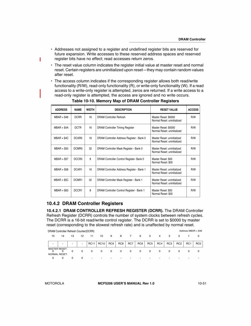
DRAM Controller
MOTOROLA MCF5206 USERÕS MANUAL Rev 1.0 10-51
2
3
4
5
6
7
8
9
10
11
12
13
14
15
16
1¥ Addresses not assigned to a register and undefined register bits are reserved for
future expansion. Write accesses to these reserved address spaces and reserved register bits have no effect; read accesses return zeros.
¥ The reset value column indicates the register initial value at master reset and normal reset. Certain registers are uninitialized upon resetÑthey may contain random values after reset.
¥ The access column indicates if the corresponding register allows both read/write functionality (R/W), read-only functionality (R), or write-only functionality (W). If a read access to a write-only register is attempted, zeros are returned. If a write access to a read-only register is attempted, the access are ignored and no write occurs.
10.4.2 DRAM Controller Registers10.4.2.1 DRAM CONTROLLER REFRESH REGISTER (DCRR). The DRAM Controller Refresh Register (DCRR) controls the number of system clocks between refresh cycles. The DCRR is a 16-bit read/write control register. The DCRR is set to $0000 by master reset (corresponding to the slowest refresh rate) and is unaffected by normal reset.
Table 10-10. Memory Map of DRAM Controller Registers
ADDRESS NAME WIDTH DESCRIPTION RESET VALUE ACCESS
MBAR + $46 DCRR 16 DRAM Controller Refresh Master Reset: $0000Normal Reset: uninitialized
R/W
MBAR + $4A DCTR 16 DRAM Controller Timing Register Master Reset: $0000Normal Reset: uninitialized
R/W
MBAR + $4C DCAR0 16 DRAM Controller Address Register - Bank 0 Master Reset: uninitializedNormal Reset: uninitialized
R/W
MBAR + $50 DCMR0 32 DRAM Controller Mask Register - Bank 0 Master Reset: uninitializedNormal Reset: uninitialized
R/W
MBAR + $57 DCCR0 8 DRAM Controller Control Register- Bank 0 Master Reset: $00Normal Reset: $00
R/W
MBAR + $58 DCAR1 16 DRAM Controller Address Register - Bank 1 Master Reset: uninitializedNormal Reset: uninitialized
R/W
MBAR + $5C DCMR1 32 DRAM Controller Mask Register - Bank 1 Master Reset: uninitializedNormal Reset: uninitialized
R/W
MBAR + $63 DCCR1 8 DRAM Controller Control Register - Bank 1 Master Reset: $00Normal Reset: $00
R/W
- - - - RC11 RC10 RC9 RC8 RC7 RC6 RC5 RC4 RC3 RC2 RC1 RC0
15 14 13 12 11 10 9 8 7 6 5 4 3 2 1 0
0 0 0 0 0 0 0 0 0 0 0 0 0 0 0 0MASTER RESET:
DRAM Controller Refresh Counter(DCRR) Address MBAR + $46
NORMAL RESET:
0 0 0 0 - - - - - - - - - - - -

2
3
4
5
6
7
8
9
10
11
12
13
14
15
16
1DRAM Controller
10-52 MCF5206 USERÕS MANUAL Rev 1.0 MOTOROLA
RC11 - RC0 - Refresh CountThis field controls the frequency of refresh requests. The value stored in this field is multiplied by 16 system clocks to determine the refresh period. The refresh period can range from 16 system clocks to 65,536 system clocks. An RC field value of all zeros corresponds to 65,536 system clocks. Any write to the DCRR forces a refresh cycle to occur. The refresh period can be calculated using the following equations:
For RC>$000:
Refresh period = RC x16 x (1/system clock frequency)
For RC=$000:
Refresh period = 65536 x (1/system clock frequency)
10.4.2.2 DRAM CONTROLLER TIMING REGISTER (DCTR). The DCTR controls the waveform timing for all DRAM transfers. The fields in this register control the RAS and CAS waveform timing for all types of DRAM transfers provided by the DRAMC. The DCTR is a 16-bit read/write control register. The DCTR is set to $0000 by master reset and is unaffected by normal reset.
DAEM - Drive Multiplexed Address During External Master DRAM transfersThis field controls the MCF5206 output driver enables for the external address bus during external master transfers that hit in DRAM address space. If DAEM is set to 1, the portion of A[27]/CS[7]/WE[0], A[26]/CS[6]/WE[1], A[25]/CS[5]/WE[2], A[24]/CS[4]/WE[3] that are configured as address signals are driven along with A[23:0] to provide row and column address multiplexing for external masters. This field does not affect the address multiplexing for DRAM transfers initiated by the ColdFire core.
0 = Do not drive the external address signals as outputs during external master DRAM transfers
1 = Drive the external address signals as outputs to provide row and column address multiplexing during external master DRAM transfers
EDO - Extended Data-Out EnableThis field controls page mode CAS timing. If the DRAM banks are populated with extended data-out DRAM, the EDO Enable bit can be set to take advantage of the CAS timing allowed by EDO DRAMs. The EDO Enable bit, along with the CAS and CP bits,
DAEM EDO - RCD - RSH1 RSH0 - - RP1 RP0 - CAS - CP CSR
15 14 13 12 11 10 9 8 7 6 5 4 3 2 1 0
0 0 0 0 0 0 0 0 0 0 0 0 0 0 0 0MASTER RESET:
DRAM Controller Timing Register(DCTR) Address MBAR + $4A
NORMAL RESET:- - 0 - 0 - - 0 0 - - 0 - 0 - -
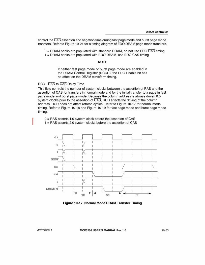
DRAM Controller
MOTOROLA MCF5206 USERÕS MANUAL Rev 1.0 10-53
2
3
4
5
6
7
8
9
10
11
12
13
14
15
16
1control the CAS assertion and negation time during fast page mode and burst page mode transfers. Refer to Figure 10-21 for a timing diagram of EDO DRAM page mode transfers.
0 = DRAM banks are populated with standard DRAM, do not use EDO CAS timing1 = DRAM banks are populated with EDO DRAM, use EDO CAS timing
NOTE
If neither fast page mode or burst page mode are enabled inthe DRAM Control Register (DCCR), the EDO Enable bit hasno affect on the DRAM waveform timing.
RCD - RAS-to-CAS Delay TimeThis field controls the number of system clocks between the assertion of RAS and the assertion of CAS for transfers in normal mode and for the initial transfer to a page in fast page mode and burst page mode. Because the column address is always driven 0.5 system clocks prior to the assertion of CAS, RCD affects the driving of the column address. RCD does not affect refresh cycles. Refer to Figure 10-17 for normal mode timing. Refer to Figure 10-18 and Figure 10-19 for fast page mode and burst page mode timing.
0 = RAS asserts 1.0 system clock before the assertion of CAS1 = RAS asserts 2.0 system clocks before the assertion of CAS
Figure 10-17. Normal Mode DRAM Transfer Timing
CLK
TS
A
RAS
CAS
D
INTERNAL TA
DRAMW
RCD RSH RP
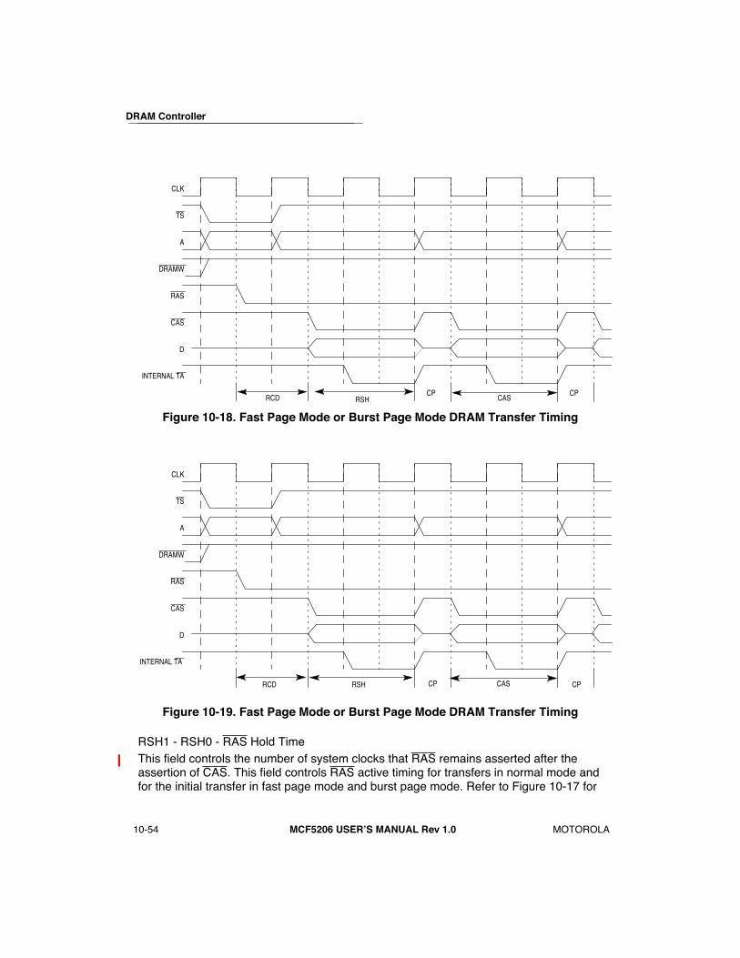
2
3
4
5
6
7
8
9
10
11
12
13
14
15
16
1DRAM Controller
10-54 MCF5206 USERÕS MANUAL Rev 1.0 MOTOROLA
Figure 10-18. Fast Page Mode or Burst Page Mode DRAM Transfer Timing
Figure 10-19. Fast Page Mode or Burst Page Mode DRAM Transfer Timing
RSH1 - RSH0 - RAS Hold TimeThis field controls the number of system clocks that RAS remains asserted after the assertion of CAS. This field controls RAS active timing for transfers in normal mode and for the initial transfer in fast page mode and burst page mode. Refer to Figure 10-17 for
CLK
TS
A
RAS
CAS
D
INTERNAL TA
DRAMW
RCD RSHCP CP
CAS
CLK
TS
A
RAS
CAS
D
INTERNAL TA
DRAMW
RCD RSH CP CPCAS

DRAM Controller
MOTOROLA MCF5206 USERÕS MANUAL Rev 1.0 10-55
2
3
4
5
6
7
8
9
10
11
12
13
14
15
16
1normal mode timing. Refer to Figure 10-19 and Figure 10-21 for fast-page-mode and burst- page-mode timing.
For transfers in normal mode:
00 = RAS negates 1.5 system clocks after the assertion of CAS01 = RAS negates 2.5 system clocks after the assertion of CAS10 = RAS negates 3.5 system clocks after the assertion of CAS11 = Reserved
For the initial transfer in fast page mode and burst page mode with EDO Enable = 0:
00 = RAS negates 1.5 system clocks after the assertion of CAS01 = RAS negates 2.5 system clocks after the assertion of CAS10 = RAS negates 3.5 system clocks after the assertion of CAS11 = Reserved
For initial transfer in fast page mode and burst page mode with EDO Enable = 1:
00 = RAS negates 1.0 system clocks after the assertion of CAS01 = RAS negates 2.0 system clocks after the assertion of CAS10 = RAS negates 3.0 system clocks after the assertion of CAS11 = Reserved
RP1 - RP0 - RAS Precharge TimeThis field controls the number of system clocks RAS precharges when the bus master requires back-to-back DRAM transfers in normal mode. RP also controls the number system clocks RAS precharges after a refresh cycle or when a page is closed in fast page mode or burst page mode. Refer to Figure 10-22 for refresh cycle timing. Refer to Figure 10-17 for normal mode timing. Refer to Figure 10-20 for fast page-mode timing.
00 = RAS precharges for 1.5 system clocks01 = RAS precharges for 2.5 system clocks 10 = RAS precharges for 3.5 system clocks11 = Reserved

2
3
4
5
6
7
8
9
10
11
12
13
14
15
16
1DRAM Controller
10-56 MCF5206 USERÕS MANUAL Rev 1.0 MOTOROLA
Figure 10-20. Fast Page Mode Page Hit and Page Miss DRAM Transfer Timing
CAS - Column Address Strobe TimeThis field, together with the EDO field, controls the number of system clocks that CAS is asserted on transfers once a page is open in fast page mode and burst page mode. Refer to Figure 10-18 for timing diagrams of fast-page-mode or burst-page- mode transfers to standard DRAMs and Figure 10-21 for fast-page-mode or burst-page-mode transfers to EDO DRAMs.
For EDO = 0:
0 = CAS is asserted for 1.5 system clocks1 = CAS is asserted for 2.5 system clocks
For EDO = 1:
0 = CAS is asserted for 1.0 system clock1 = CAS is asserted for 2.0 system clocks
CLK
TS
A
RAS
CAS
D
INTERNAL TA
DRAMW
CAS RP
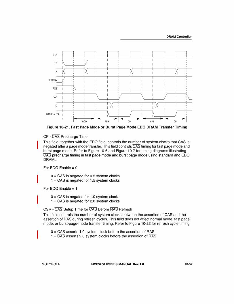
DRAM Controller
MOTOROLA MCF5206 USERÕS MANUAL Rev 1.0 10-57
2
3
4
5
6
7
8
9
10
11
12
13
14
15
16
1
Figure 10-21. Fast Page Mode or Burst Page Mode EDO DRAM Transfer Timing
CP - CAS Precharge TimeThis field, together with the EDO field, controls the number of system clocks that CAS is negated after a page mode transfer. This field controls CAS timing for fast page mode and burst page mode. Refer to Figure 10-6 and Figure 10-7 for timing diagrams illustrating CAS precharge timing in fast page mode and burst page mode using standard and EDO DRAMs.
For EDO Enable = 0:
0 = CAS is negated for 0.5 system clocks1 = CAS is negated for 1.5 system clocks
For EDO Enable = 1:
0 = CAS is negated for 1.0 system clock1 = CAS is negated for 2.0 system clocks
CSR - CAS Setup Time for CAS Before RAS RefreshThis field controls the number of system clocks between the assertion of CAS and the assertion of RAS during refresh cycles. This field does not affect normal mode, fast page mode, or burst-page-mode transfer timing. Refer to Figure 10-22 for refresh cycle timing.
0 = CAS asserts 1.0 system clock before the assertion of RAS1 = CAS asserts 2.0 system clocks before the assertion of RAS
CLK
TS
A
RAS
CAS
D
INTERNAL TA
DRAMW
RCD RSH CP CAS CP
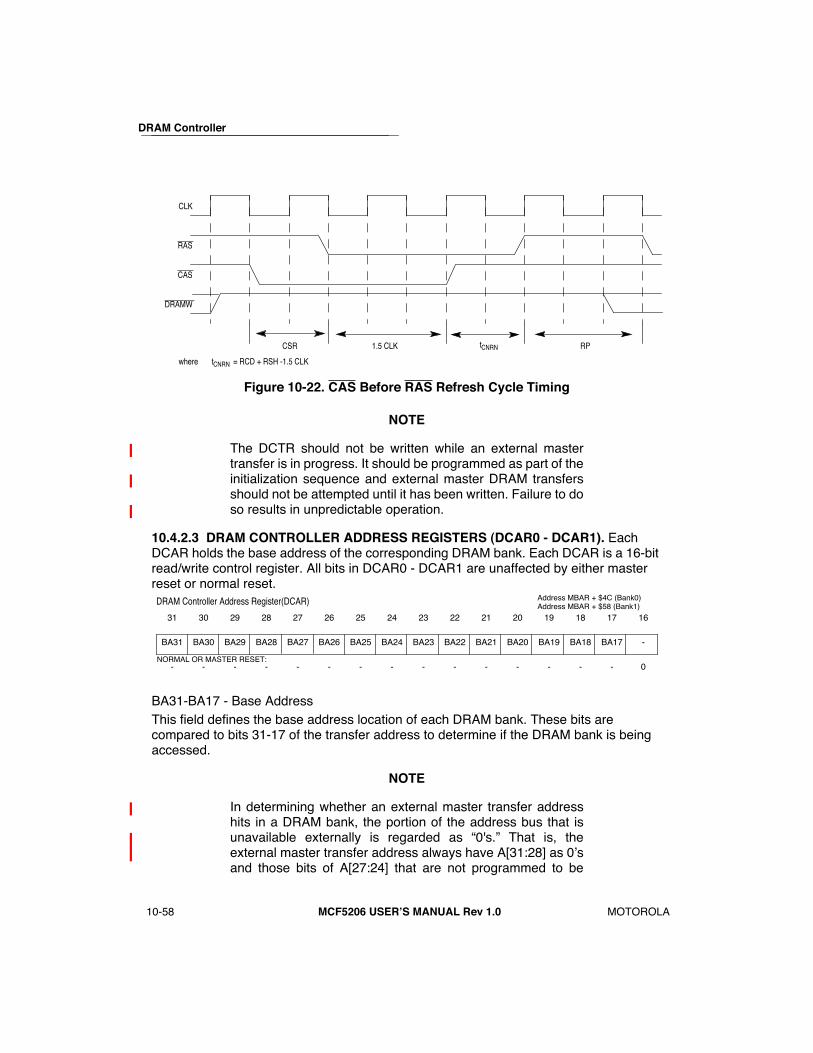
2
3
4
5
6
7
8
9
10
11
12
13
14
15
16
1DRAM Controller
10-58 MCF5206 USERÕS MANUAL Rev 1.0 MOTOROLA
Figure 10-22. CAS Before RAS Refresh Cycle Timing
NOTE
The DCTR should not be written while an external mastertransfer is in progress. It should be programmed as part of theinitialization sequence and external master DRAM transfersshould not be attempted until it has been written. Failure to doso results in unpredictable operation.
10.4.2.3 DRAM CONTROLLER ADDRESS REGISTERS (DCAR0 - DCAR1). Each DCAR holds the base address of the corresponding DRAM bank. Each DCAR is a 16-bit read/write control register. All bits in DCAR0 - DCAR1 are unaffected by either master reset or normal reset.
BA31-BA17 - Base AddressThis field defines the base address location of each DRAM bank. These bits are compared to bits 31-17 of the transfer address to determine if the DRAM bank is being accessed.
NOTE
In determining whether an external master transfer addresshits in a DRAM bank, the portion of the address bus that isunavailable externally is regarded as Ò0's.Ó That is, theexternal master transfer address always have A[31:28] as 0Õsand those bits of A[27:24] that are not programmed to be
CLK
RAS
CAS
DRAMW
CSR 1.5 CLK tCNRN
tCNRN = RCD + RSH -1.5 CLK
RP
where
BA31 BA30 BA29 BA28 BA27 BA26 BA25 BA24 BA23 BA22 BA21 BA20 BA19 BA18 BA17 -
31 30 29 28 27 26 25 24 23 22 21 20 19 18 17 16
- - - - - - - - - - - - - - - 0NORMAL OR MASTER RESET:
DRAM Controller Address Register(DCAR) Address MBAR + $4C (Bank0)Address MBAR + $58 (Bank1)

DRAM Controller
MOTOROLA MCF5206 USERÕS MANUAL Rev 1.0 10-59
2
3
4
5
6
7
8
9
10
11
12
13
14
15
16
1external address bits as 0Õs. In order for a bank to beaccessible to an external master, the address bits that areunavailable to the external master must either be set to 0 in theDCAR or be masked in the DCMR.
10.4.2.4 DRAM CONTROLLER MASK REGISTER (DCMR0 - DCMR1). Each DCMR holds the address mask for each of the DRAM banks as well the definition of which types of transfers are allowed for the DRAM banks. Each DCMR is a 32-bit read/write control register. All bits in DCMR0 - DCMR1 are unaffected by either Master Reset or normal reset.
BAM31-BAM17 - Base Address MaskThis field defines the DRAM address space through the use of address mask bits. Any bit set to 1 masks the corresponding base address register (DCAR) bit (the base address bit becomes a ÔÔdonÕt careÕÕ in the address comparison). Unmasked base address bits are compared to the ColdFire core or external master transfer address to determine if the transfer is accessing a DRAM address space.
0 = Corresponding address bit is used in DRAM bank decode1 = Corresponding address bit is a ÔÔdonÕt careÕÕ in DRAM bank decode
SC, SD, UC, UD - Supervisor Code, Supervisor Data, User Code, User Data TransferMaskThis field masks allows specific types of transfers to be inhibited from accessing the DRAM bank. If a transfer mask bit is cleared, a transfer of that type can access the corresponding DRAM bank. If a transfer mask bit is set to 1, an transfer of that type can not access the corresponding DRAM bank. The transfer mask bits are:
SC = Supervisor Code maskSD = Supervisor Data maskUC = User Code maskUD = User Data mask
BAM31 BAM30 BAM29 BAM28 BAM27 BAM26 BAM25 BAM24 BAM23 BAM22 BAM21 BAM20 BAM19 BAM18 BAM17 -
31 30 29 28 27 26 25 24 23 22 21 20 19 18 17 16
- - - - - - - - - - - - - - - 0NORMAL OR MASTER RESET:
- - - - - - - - - - - SC SD UC UD -
15 14 13 12 11 10 9 8 7 6 5 4 3 2 1 0
0 0 0 0 0 0 0 0 0 0 0 - - - - 0NORMAL OR MASTER RESET:
DRAM Controller Mask Register(DCMR) Address MBAR + $50 (Bank0)Address MBAR + $5C (Bank1)

2
3
4
5
6
7
8
9
10
11
12
13
14
15
16
1DRAM Controller
10-60 MCF5206 USERÕS MANUAL Rev 1.0 MOTOROLA
For each transfer mask bit:0 = Do not mask this type of transfer for the DRAM bank. A transfer of this type can
access the DRAM bank1 = Mask this type of transfer for the DRAM bank. A transfer of this type cannot
access the DRAM bank
NOTE
The SC, SD, UC, and UD bits are ignored during externalmaster transfers. Therefore, an external master transfer canaccess the DRAM banks regardless of the transfer masks.
NOTE
In determining whether an external master transfer addresshits in a DRAM bank, the portion of the address bus that isunavailable externally are regarded as Ò0's.Ó That is, theexternal master transfer address always have A[31:28] as 0Õsand those bits of A[27:24] that are not programmed to beexternal address bits as 0Õs. In order for a bank to beaccessible to an external master, the address bits that areunavailable to the external master must either be set to 0 inthe DCAR or be masked in the DCMR.
10.4.2.5 DRAM CONTROLLER CONTROL REGISTER (DCCR0 - DCCR1). Each DCCR specifies the port size, page size, page mode, and activation of each of the DRAM banks. Each DCCR is an 8-bit read/write control register. Master reset and normal reset set all bits to zero.
PS - Port SizeThis field specifies the data width of the DRAM bank. PS determines the byte lanes that data is driven on during write cycles and the byte lanes that data is sampled from during read cycles.
00 = 32-bit port size - Data sampled and driven on D[31:0]01 = 8-bit port size - Data sampled and driven on D[31:24] only10 = 16-bit port size - Data sampled and driven on D[31:16] only11 = 16-bit port size - Data sampled and driven on D[31:16] only
PS1 PS0 BPS1 BPS0 PM1 PM0 WR RD
7 6 5 4 3 2 1 0
0 0 0 0 0 0 0 0NORMAL OR MASTER RESET:
DRAM Controller Control Register(DCCR)Address MBAR + $57 (Bank0)Address MBAR + $63 (Bank1)

2
3
4
5
6
7
8
9
10
11
12
13
14
15
16
1DRAM Controller
10-61 MCF5206 USERÕS MANUAL Rev 1.0 MOTOROLA
BPS - Bank Page SizeThis field defines the bank page size for each DRAM bank for fast page mode and burst page mode.
00 = 512 byte page size01 = 1 KByte page size10 = 2 KByte page size11 = Reserved
PM - Page Mode SelectThis field selects the type of DRAM transfers generated for each DRAM bank: normal mode, fast page mode, or burst-page-mode transfers.
00 = Normal Mode01 = Burst Page Mode10 = Reserved11 = Fast Page Mode
WR - Write EnableThis field controls whether the DRAM bank can be accessed during write transfers.
0 = Do not activate DRAM control signals on write transfers1 = Activate DRAM control signals on write transfers
RD - Read EnableThis field controls whether the DRAM bank can be accessed during read transfers.
0 = Do not activate DRAM control signals on read transfers1 = Activate DRAM control signals on read transfers
10.5 DRAM INITIALIZATION EXAMPLEThe following sample of assembly program illustrates a DRAM initialization procedure. DRAM bank 0 is configured for a 4 MByte DRAM starting at address 0x00100000. The DRAM port size is programmed to 32-bit (1 MByte x 32), the page size to 512 byte, and fast page mode is enabled.
The Module Base Address Register (MBAR) is first written with the MODULE_BASE value. This locates all the MCF5206 internal modules at address 0x00004000. Then the DRAM Controller Timing Register (DCTR) is initialized to give the fastest possible DRAM transfer waveform timing. The DRAM Controller Refresh Register (DCRR) is then written causing DRAM refresh cycles to be generated once every 512 clocks (15.4 msec for a 33 MHz system clock). Once the DCRR is written, a refresh cycle is immediately generated and refresh cycles start being generated at the newly programmed rate. Next, DRAM Controller Address Register 0 (DCAR0) is written, making the starting address of DRAM bank 0 0x00100000. DRAM Controller Mask Register 0 (DCMR0) is then written such that transfer address bits 18 - 16 are masked, making the DRAM bank 0 address space 1

2
3
4
5
6
7
8
9
10
11
12
13
14
15
16
1DRAM Controller
10-62 MCF5206 USERÕS MANUAL Rev 1.0 MOTOROLA
MByte. Therefore, DRAM bank 0 address space ranges from 0x00100000 - 0x001EFFFF. DRAM Controller Control Register 0 (DCCR0) is then written making DRAM bank 0 have a 32-bit port size, a 512 byte bank page size, generate fast-page-mode transfers, and be enabled for both read transfers and write transfers. At this point, DRAM bank 0 is initialized; however, DRAM read and write transfers are not generated until the global chip select is disabled by writing CSMR0.
# set up variables
MODULE_BASE equ 0x00004001 Base address of internal module registersDRAM0_BASE equ 0x0010 Base address for Bank0 DRAMDCRRequ 0x46 DRAMC Refresh RegisterDCTRequ 0x4a DRAMC Timing RegisterDCAR0equ 0x4c DRAMC Address Register 0DCMR0equ 0x50 DRAMC Mask Register 0DCCR0equ 0x57 DRAMC Control Register 0CSMR0equ 0x68 Chip select Mask Register 0
# DRAMC initialization
move.l #MODULE_BASE, d0 Initialize MBARmovec d0, mbarmove.l #MODULE_BASE, a0 a0 points to the module base address
move.w #0x00, d0 Initialize for fastest DRAM cycle timingmove.w d0, (DCTR, a0) (RCD=RSH1=RSH0=RP1=RP0=CAS=CP=CSR=0)
move.w #0x20, d0 Refresh every 512 clocks (15.4 uS @ 33Mhz)move.w d0, (DCRR, a0)
move.w #DRAM0_BASE, d0 Set DRAM0 start address at 0x00100000move.w d0, (DCAR0, a0)
move.l #0x000e0000, d0 Mask low order bits for 1Mbyte address spacemove.l d0, (DCMR0, a0) DRAM0 address space is 0x0010-0x001effff
move.b #0x0f, d0 32-bit port, 512-byte page, fast page mode,move.b d0, (DCCR0, a0) Readable/writable
# The global chip select activates for ALL external transfers after reset untilit is disabled. Therefore, before a DRAM transfer can be done, the global chipselect must be disabled by writing CSMR0.

MOTOROLA
MCF5206 USERÕS MANUAL Rev 1.0
11-1
SECTION 11UART MODULES
The MCF5206 contains two universal asynchronous/synchronous receiver/transmitters (UARTs) that act independently. Each UART is clocked by the system clock, which eliminates the need for an external crystal.
Each UART module, shown in Figure 11-1, consists of the following major functional areas:
¥ Serial Communication Channel
¥ 16-Bit Baud-RateTimer
¥ Internal Channel Control Logic
¥ Interrupt Control Logic
Figure 11-1. UART Block Diagram
INTERNAL CHANNELCONTROL LOGIC
INTERRUPT CONTROLLOGIC
16-BIT TIMERFOR BAUD RATE GENERATION
SERIAL COMMUNICATIONCHANNEL
CTS
RTS
RXD
TXD
SYSTEM CLOCK
TIN (EXT CLK)
DATE: 9-2-98
REVISION NO.: 1.1
PAGES AFFECTED: SEE CHANGE BARS

UART Modules
11-2
MCF5206 USERÕS MANUAL Rev 1.0
MOTOROLA
11.1 MODULE OVERVIEW
The MCF5206 contains two independent UART modules. Features of each UART module include the following:
¥ UART clocked by the system clock or external clock (TIN)
¥ Full duplex asynchronous/synchronous receiver/transmitter channel
¥ Quadruple-buffered receiver
¥ Double-buffered transmitter
¥ Independently programmable baud rate for receiver and transmitter selectable from:Ñ timer-generated baud rate or external clock
¥ Programmable data format:
Ñ Five to eight data bits plus parityÑ Odd, even, no parity, or force parityÑ .563 to 2 stop bits in x16 mode(asynchronous)/1or 2 stop bits in synchronous
mode
¥ Programmable channel modes:
Ñ Normal (full duplex)Ñ Automatic echoÑ Local loopbackÑ Remote loopback
¥ Automatic wakeup mode for multidrop applications
¥ Four maskable interrupt conditions
¥ Parity, framing, break, and overrun error detection
¥ False start bit detection
¥ Line-break detection and generation
¥ Detection of breaks originating in the middle of a character
¥ Start/end break interrupt/status
11.1.1 Serial Communication Channel
The communication channel provides a full duplex asynchronous/synchronous receiver and transmitter using an operating frequency derived from the system clock or from an external clock tied to the TIN pin.
The transmitter accepts parallel data from the CPU; converts it to a serial bit stream; inserts the appropriate start, stop, and optional parity bits; then outputs a composite serial data stream on the channel transmitter serial data output (TxD). Refer to
Section 11.3.3.1 Transmitter
for additional information.

UART Modules
MOTOROLA
MCF5206 USERÕS MANUAL Rev 1.0
11-3
The receiver accepts serial data on the channel receiver serial data input (RxD); converts it to parallel format; checks for a start bit, stop bit, parity (if any), or any error condition; and transfers the assembled character onto the bus during read operations. The receiver can be polled or interrupt driven. Refer to
Section 11.3.3.2 Receiver
for additional information.
11.1.2 Baud-Rate Generator/Timer
The 16-bit timer, clocked by the system clock, can function as an asynchronous x16 clock. In addition, you can tie an external clock to one of the TIN pins of a MCF5206 timer for use as a synchronous or asynchronous clocking source for the UART. The baud-rate timer is part of each UART and not related to the ColdFire timer modules.
11.1.3 Interrupt Control Logic
An Internal Interrupt Request signal (IRQ) notifies the MCF5206 interrupt controller of an interrupt condition. The output is the logical NOR of all (as many as four) unmasked interrupt status bits in the UART Interrupt Status Register (UISR). You program the UART Interrupt Mask Register (UIMR) to determine which interrupts is valid in the UISR.
You program the UART module interrupt level in the MCF5206 interrupt controller external to the UART module. You can configure the UART to supply the vector from the UART Interrupt Vector Register (UIVR) or program the SIM to provide an autovector when a UART interrupt is acknowledged.
You can also program the interrupt level, priority within the level, and autovectoring capability in the SIM register ICR_U1.
11.2 UART MODULE SIGNAL DEFINITIONS
The following paragraphs contain a brief description of the UART module signals. Figure 11-2 shows both the external and internal signal groups.
NOTE
The terms
assertion
and
negation
are used throughout thissection to avoid confusion when dealing with a mixture ofactive-low and active-high signals. The term
assert
or
assertion
indicates that a signal is active or true, independentof the level represented by a high or low voltage. The term
negate
or
negation
indicates that a signal is inactive or false.
11.2.1 Transmitter Serial Data Output (TxD)
This signal is the transmitter serial data output. The output is held high ('ÔmarkÕ' condition) when the transmitter is disabled, idle, or operating in the local loopback mode. Data is shifted out on this signal on the falling edge of the clock source, with the least significant bit transmitted first. All UART pins are muxed with the parallel port. On UART 2, RTS is

UART Modules
11-4
MCF5206 USERÕS MANUAL Rev 1.0
MOTOROLA
muxed with RESET at the pin. Their functionality is determined by programming the Pin Assignment Register (PAR) in the SIM.
11.2.2 Receiver Serial Data Input (RxD)
This signal is the receiver serial data input. Data received on this signal is sampled on the rising edge of the clock source, with the least significant bit received first.
11.2.3 Request-To-Send (RTS)
You can program this active-low output signal to be automatically negated and asserted by either the receiver or transmitter. When connected to the clear-to-send (CTS) input of a transmitter, this signal controls serial data flow.
11.2.4 Clear-To-Send (CTS)
This active-low input is the clear-to-send input and can generate an interrupt on change-of-state.
Figure 11-2. External and Internal Interface Signals
INTERNAL
CONTROL
LOGIC
FOUR-CHARACTERRECEIVE BUFFER
TWO-CHARACTERTRANSMIT BUFFER
INPUT PORT
OUTPUT PORT
EXTE
RN
AL IN
TER
FAC
E SI
GN
ALS
INTE
RFA
CE
TO C
PU
UAR
T M
OD
ULE
INTE
RN
AL B
US
ADDRESS BUS
CONTROL
DATA
16-BIT TIMER/BAUD RATE GENERATOR
SYSTEM CLOCK
IRQ
CTS
RTS
RXD
TXD
TIN(EXTCLK)
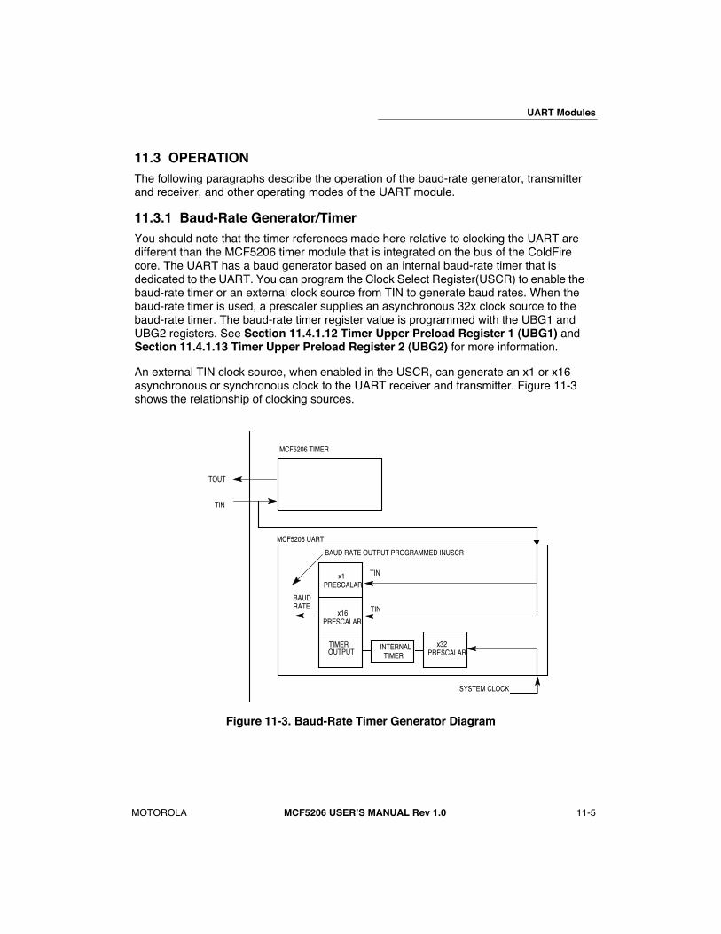
UART Modules
MOTOROLA
MCF5206 USERÕS MANUAL Rev 1.0
11-5
11.3 OPERATION
The following paragraphs describe the operation of the baud-rate generator, transmitter and receiver, and other operating modes of the UART module.
11.3.1 Baud-Rate Generator/Timer
You should note that the timer references made here relative to clocking the UART are different than the MCF5206 timer module that is integrated on the bus of the ColdFire core. The UART has a baud generator based on an internal baud-rate timer that is dedicated to the UART. You can program the Clock Select Register(USCR) to enable the baud-rate timer or an external clock source from TIN to generate baud rates. When the baud-rate timer is used, a prescaler supplies an asynchronous 32x clock source to the baud-rate timer. The baud-rate timer register value is programmed with the UBG1 and UBG2 registers. See
Section 11.4.1.12 Timer Upper Preload Register 1 (UBG1)
and
Section 11.4.1.13 Timer Upper Preload Register 2 (UBG2)
for more information.
An external TIN clock source, when enabled in the USCR, can generate an x1 or x16 asynchronous or synchronous clock to the UART receiver and transmitter. Figure 11-3 shows the relationship of clocking sources.
Figure 11-3. Baud-Rate Timer Generator Diagram
MCF5206 UART
MCF5206 TIMER
TIN
TOUT
TIN
SYSTEM CLOCK
x1 PRESCALAR
x16 PRESCALAR
TIMEROUTPUT
INTERNALTIMER
x32PRESCALAR
TINBAUDRATE
BAUD RATE OUTPUT PROGRAMMED INUSCR

UART Modules
11-6
MCF5206 USERÕS MANUAL Rev 1.0
MOTOROLA
11.3.2 Uart Baud Rate Table
Table 11.1 provides a convenient table for determining standard buad rates on theMCF5206. The calculation for determining baud rates is as follows:
Baud Rate calculation
baud rate = [Bus clock frequency]/(32*(baud prescale of UBG1&2)
For example, if the bus clock was operating at 45mhz and a 9600 baud rate was needed,the calculation would be:
9600 = [45 x 10^6]/(32 x UBG1&2 prescale)
The prescale value would be 146 decimal ($0092 hex). Therefore UBG1 (msb) would beprogramed with $00 and UBG2 (lsb) would be programmed with $92.
Note
The minimum value that can be programmed into the concatenation of UBG1 and UBG2is $0002. Also, the values for some of the calculated baud rates below are approximationsdue to decimal rounding error (i.e. 9600 baud @ 33mhz is really 9637.85 baud).
Table 11-1. Baud Rate Table
Baud RateDecimal Value
for UBG1&2UBG1 UBG2
300 4688 12 AF1200 1172 04 932400 586 02 494800 293 01 249600 146 00 9219.2K 73 00 4928.8K 49 00 3033.6K 42 00 2938.4K 37 00 2457.6K 24 00 1867.2K 21 00 1476800 18 00 1286400 16 00 1096000 15 00 0E115200 12 00 0C230400 6 00 06
33 MHz bus clock
300 3438 D 6D1200 859 3 5B2400 430 1 AD4800 215 0 D69600 107 0 6B

UART Modules
MOTOROLA
MCF5206 USERÕS MANUAL Rev 1.0
11-7
11.3.3 Transmitter and Receiver Operating Modes
The functional block diagram of the transmitter and receiver, including command and operating registers, is shown in Figure 11-4. The following paragraphs describe these functions in reference to this diagram. For detailed register information, refer to subsection
11.4 Register Description and Programming
.
11.3.3.1 TRANSMITTER.
The transmitter is enabled through the UART command register (UCR) located within the UART module. The UART module signals the CPU when it is ready to accept a character by setting the transmitter-ready bit (TxRDY) in the UART status register (USR). Functional timing information for the transmitter is shown in Figure 11-5.
19.2K 54 0 3528.8K 36 0 2333.6K 31 0 1E38.4K 27 0 1A57.6K 18 0 1167.2K 15 0 0F76800 13 0 0D86400 12 0 0B96000 11 0 0A115200 9 0 8230400 4 0 4
22.5 MHz bus clock
300 2344 9 271200 586 2 492400 293 0 244800 146 0 929600 73 0 4919.2K 37 0 2428.8K 24 0 1833.6K 21 0 1438.4K 18 0 1257.6K 12 0 0C67.2K 10 0 0A76800 9 0 986400 8 0 896000 7 0 7115200 6 0 6230400 3 0 3
Table 11-1. Baud Rate Table
Baud RateDecimal Value
for UBG1&2UBG1 UBG2
UART Modules
11-8
MCF5206 USERÕS MANUAL Rev 1.0
MOTOROLA
The transmitter converts parallel data from the CPU to a serial bit stream on TxD. It automatically sends a start bit followed by
¥ The programmed number of data bits
¥ An optional parity bit
¥ The programmed number of stop bits
The least significant bit is sent first. Data is shifted from the transmitter output on the falling edge of the clock source.
After the transmission of the stop bits, if a new character is not available in the transmitter holding register, the TxD output remains in the high (mark condition) state, and the transmitter-empty bit (TxEMP) in the USR is set. Transmission resumes and the TxEMP bit is cleared when the CPU loads a new character into the UART transmitter buffer (UTB). If the transmitter receives a Disable command, it continues operating until the character (if one is present) in the transmit-shift register is completely shifted out of transmitter TxD. If the transmitter is reset through a software command, operation ceases immediately (refer to subsection
Section 11.4.1.5 Command Register (UCR)
). The transmitter is re-enabled through the UCR to resume operation after a disable or software reset.
If clear-to-send operation is enabled, CTS must be asserted for the character to be transmitted. If CTS is negated in the middle of a transmission, the character in the shift register is transmitted and following the completion of STOP bits TxD, enters in the mark state until CTS is asserted again. If the transmitter is forced to send a continuous low condition by issuing a Send-Break command, the transmitter ignores the state of CTS.
You can program the transmitter to automatically negate the request-to-send (RTS) output on completion of a message transmission. If the transmitter is programmed to operate in this mode, RTS must be manually asserted before a message is transmitted. In applications where the transmitter is disabled after transmission is complete and RTS is appropriately programmed, RTS is negated one bit time after the character in the shift register is completely transmitted. You must manually enable the transmitter by setting the enable-transmitter bit in the UART Command Register (UCR).

UART Modules
MOTOROLA
MCF5206 USERÕS MANUAL Rev 1.0
11-9
Figure 11-4. Transmitter and Receiver Functional Diagram
W
R
R/W
R/W
W
R
UART SERIAL CHANNEL
UART COMMAND REGISTER (UCR)
EXTERNAL INTERFACE
UART MODE REGISTER 1 (UMR1)
UART MODE REGISTER 2 (UMR2)
UART STATUS REGISTER (USR)
TRANSMIT HOLDING REGISTER
TRANSMIT SHIFT REGISTER
RECEIVER HOLDING REGISTER 1
RECEIVER HOLDING REGISTER 2
RECEIVER HOLDING REGISTER 3
RECEIVER SHIFT REGISTER
TRANSMITBUFFER (UTB)(2 REGISTERS)
RECEIVEBUFFER (URB)(4 REGISTERS)
FIFO
TXD
RXD
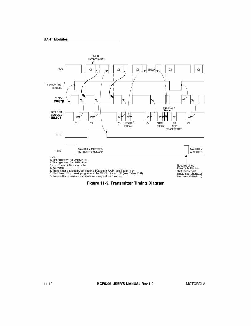
UART Modules
11-10
MCF5206 USERÕS MANUAL Rev 1.0
MOTOROLA
Figure 11-5. Transmitter Timing Diagram
C1 C2 C3 C4 C6
W W W W W W W W
C1 C2 C3 C4 STOPBREAK
STARTBREAK
C5NOT
TRANSMITTED
C6
BREAK
C1 INTRANSMISSION
TxD
TRANSMITTERENABLED
TxRDY(SR2)
CS
CTS
RTS 2
1
NOTES: 1. TIMING SHOWN FOR UMR2(4) = 1 2. TIMING SHOWN FOR UMR2(5) = 1 3. CN = TRANSMIT CHARACTER 4. W = WRITE
MANUALLY ASSERTEDBY BIT- SET COMMAND
MANUALLYASSERTED
INTERNALMODULESELECT
(SR[2])
W
Trans.Disable
Negated sincetransmit buffer and shift register areempty (last characterhas been shifted out)
Notes:1. Timing shown for UMR2[4]=12. Timing shown for UMR2[5]=13. CN=Transmit 8-bit character4. W= Write5. Transmitter enabled by configuring TCx bits in UCR (see Table 11-9)6. Start break/Stop break programmed by MISCx bits in UCR (see Table 11-8)7. Transmitter is enabled and disabled using software control
5
6
7
UART Modules
MOTOROLA
MCF5206 USERÕS MANUAL Rev 1.0
11-11
11.3.3.2 RECEIVER.
The receiver is enabled through the UCR located within the UART module. Functional timing information for the receiver is shown in Figure 11-6. The receiver looks for a high-to-low (mark-to-space) transition of the start bit on RxD. When a transition is detected, the state of RxD is sampled each 16
´
clock for eight clocks, starting one-half clock after the transition (asynchronous operation) or at the next rising edge of the bit time clock (synchronous operation). If RxD is sampled high, the start bit is not valid and the search for the valid start bit repeats. If RxD is still low, a valid start bit is assumed and the receiver continues to sample the input at one-bit time intervals at the theoretical center of the bit.
This process continues until the proper number of data bits and parity (if any) is assembled and one stop bit is detected. Data on the RxD input is sampled on the rising edge of the programmed clock source. The least significant bit is received first. The data is then transferred to a receiver holding register and the RxRDY bit in the USR is set. If the character length is less than eight bits, the most significant unused bits in the receiver holding register are cleared. The Rx RDY bit in the USR is set at the one-half point of the stop bit.
After the stop bit is detected, the receiver immediately looks for the next start bit. However, if a nonzero character is received without a stop bit (framing error) and RxD remains low for one-half of the bit period after the stop bit is sampled, the receiver operates as if a new start bit is detected. The parity error (PE), framing error (FE), overrun error (OE), and received break (RB) conditions (if any) set error and break flags in the USR at the received character boundary and are valid only when the RxRDY bit in the USR is set.
If a break condition is detected (RxD is low for the entire character including the stop bit), a character of all zeros is loaded into the receiver holding register and the Receive Break (RB) and RxRDY bits in the USR are set. The RxD signal must return to a high condition for at least one-half bit time before a search for the next start bit begins.
The receiver detects the beginning of a break in the middle of a character if the break persists through the next character time. When the break begins in the middle of a character, the receiver places the damaged character in the receiver first-in-first-out (FIFO) stack and sets the corresponding error conditions and RxRDY bit in the USR. The break persists until the next character time, the receiver places an all-zero character into the receiver FIFO, and sets the corresponding RB and RxRDY bits in the USR. Interrupts can be enabled on receive break.

UART Modules
11-12
MCF5206 USERÕS MANUAL Rev 1.0
MOTOROLA
Figure 11-6. Receiver Timing Diagram
C6, C7, C8 ARE LOST
RxD
RECEIVERENABLED
RxRDY(SR0)
FFULL(SR1)
OVERRUN(SR4)
RTS (OP0)
1
STATUS DATA STATUS DATA STATUS DATA
CS
RESET BY COMMAND
UOP(0) = 1
C4C3 C5 C6 C7 C8C1 C2
NOTES: 1. Timing shown for MR1(7) = 1 2. Timing shown for MR1(6) = 0 3. R = Read 4. C = Received Character
N
R R R R RR RR
C1 C2 C3 C4C5 LOST
STATUS DATA
DUE TO RECEIVER DISABLED
2
INTERNALMODULESELECT
UOP1[0]=1NOTES:1. Timing shown for UMR1[7]=12. Timing shown for UMR1[6]=02.5Timing shown for UMR1[6]=1
2.5
3. R=Read4. CN=Received 5-8 bit character
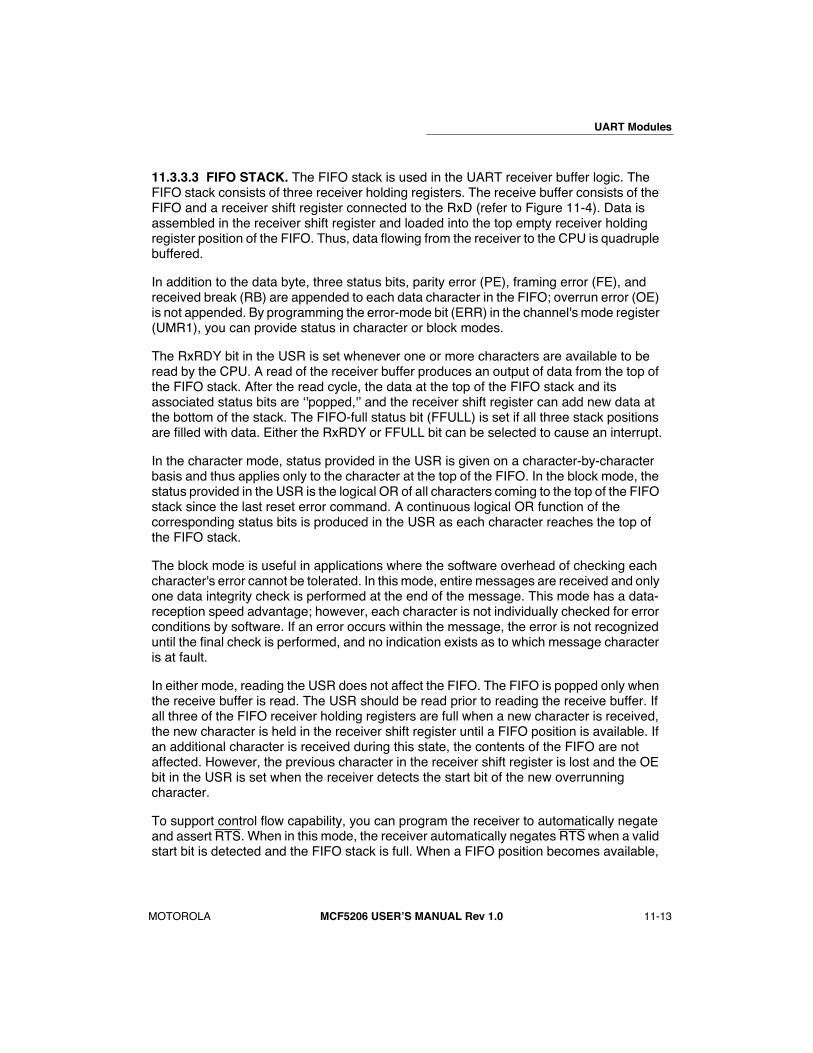
UART Modules
MOTOROLA
MCF5206 USERÕS MANUAL Rev 1.0
11-13
11.3.3.3 FIFO STACK.
The FIFO stack is used in the UART receiver buffer logic. The FIFO stack consists of three receiver holding registers. The receive buffer consists of the FIFO and a receiver shift register connected to the RxD (refer to Figure 11-4). Data is assembled in the receiver shift register and loaded into the top empty receiver holding register position of the FIFO. Thus, data flowing from the receiver to the CPU is quadruple buffered.
In addition to the data byte, three status bits, parity error (PE), framing error (FE), and received break (RB) are appended to each data character in the FIFO; overrun error (OE) is not appended. By programming the error-mode bit (ERR) in the channel's mode register (UMR1), you can provide status in character or block modes.
The RxRDY bit in the USR is set whenever one or more characters are available to be read by the CPU. A read of the receiver buffer produces an output of data from the top of the FIFO stack. After the read cycle, the data at the top of the FIFO stack and its associated status bits are Ô'popped,'Õ and the receiver shift register can add new data at the bottom of the stack. The FIFO-full status bit (FFULL) is set if all three stack positions are filled with data. Either the RxRDY or FFULL bit can be selected to cause an interrupt.
In the character mode, status provided in the USR is given on a character-by-character basis and thus applies only to the character at the top of the FIFO. In the block mode, the status provided in the USR is the logical OR of all characters coming to the top of the FIFO stack since the last reset error command. A continuous logical OR function of the corresponding status bits is produced in the USR as each character reaches the top of the FIFO stack.
The block mode is useful in applications where the software overhead of checking each character's error cannot be tolerated. In this mode, entire messages are received and only one data integrity check is performed at the end of the message. This mode has a data-reception speed advantage; however, each character is not individually checked for error conditions by software. If an error occurs within the message, the error is not recognized until the final check is performed, and no indication exists as to which message character is at fault.
In either mode, reading the USR does not affect the FIFO. The FIFO is popped only when the receive buffer is read. The USR should be read prior to reading the receive buffer. If all three of the FIFO receiver holding registers are full when a new character is received, the new character is held in the receiver shift register until a FIFO position is available. If an additional character is received during this state, the contents of the FIFO are not affected. However, the previous character in the receiver shift register is lost and the OE bit in the USR is set when the receiver detects the start bit of the new overrunning character.
To support control flow capability, you can program the receiver to automatically negate and assert RTS. When in this mode, the receiver automatically negates RTS when a valid start bit is detected and the FIFO stack is full. When a FIFO position becomes available,

UART Modules
11-14
MCF5206 USERÕS MANUAL Rev 1.0
MOTOROLA
the receiver asserts RTS. Using this mode of operation prevents overrun errors by connecting the RTS to the CTS input of the transmitting device.
To use the RTS signals on UART 2, you must set up the MCF5206 Pin Assignment Register (PAR) in the SIM to enable the corresponding I/O pins for these functions.
If the FIFO stack contains characters and the receiver is disabled, the CPU can still read the characters in the FIFO. If the receiver is reset, the FIFO stack and all receiver status bits, corresponding output ports, and interrupt request are reset. No additional characters are received until the receiver is re-enabled.
11.3.4 Looping Modes
You can configure the UART to operate in various looping modes as shown in Figure 11-7. These modes are useful for local and remote system diagnostic functions. The modes are described in the following paragraphs with additional information available in subsection
11.4 Register Description and Programming
.
You should only switch between modes while the transmitter and receiver are disabled because the selected mode is activated immediately on mode selection, even if this occurs in the middle of character transmission or reception. In addition, if a mode is deselected, the device switches out of the mode immediately, except for automatic echo and remote echo loopback modes. In these modes, the deselection occurs just after the receiver has sampled the stop bit (this is also the one-half point). For automatic echo mode, the transmitter stays in this mode until the entire stop bit has been retransmitted.
11.3.4.1 AUTOMATIC ECHO MODE.
In this mode, the UART automatically retransmits the received data on a bit-by-bit basis. The local CPU-to-receiver communication continues normally but the CPU-to-transmitter link is disabled. While in this mode, received data is clocked on the receiver clock and retransmitted on TxD. The receiver must be enabled but not the transmitter. Instead, the transmitter is clocked by the receiver clock.
Because the transmitter is not active, the TxEMP and TxRDY bits in USR are inactive and data is transmitted as it is received. Received parity is checked but not recalculated for transmission. Character framing is also checked but stop bits are transmitted as received. A received break is echoed as received until the next valid start bit is detected.
11.3.4.2 LOCAL LOOPBACK MODE.
In this mode, TxD is internally connected to RxD. This mode is useful for testing the operation of a local UART module channel by sending data to the transmitter and checking data assembled by the receiver. In this manner, correct channel operations can be assured. Both transmitter and CPU-to-receiver communications continue normally in this mode. While in this mode, the RxD input data is ignored, the TxD is held marking, and the receiver is clocked by the transmitter clock. The transmitter must be enabled but not the receiver.
11.3.4.3 REMOTE LOOPBACK MODE.
In this mode, the channel automatically transmits received data on the TxD output on a bit-by-bit basis. The local CPU-to-
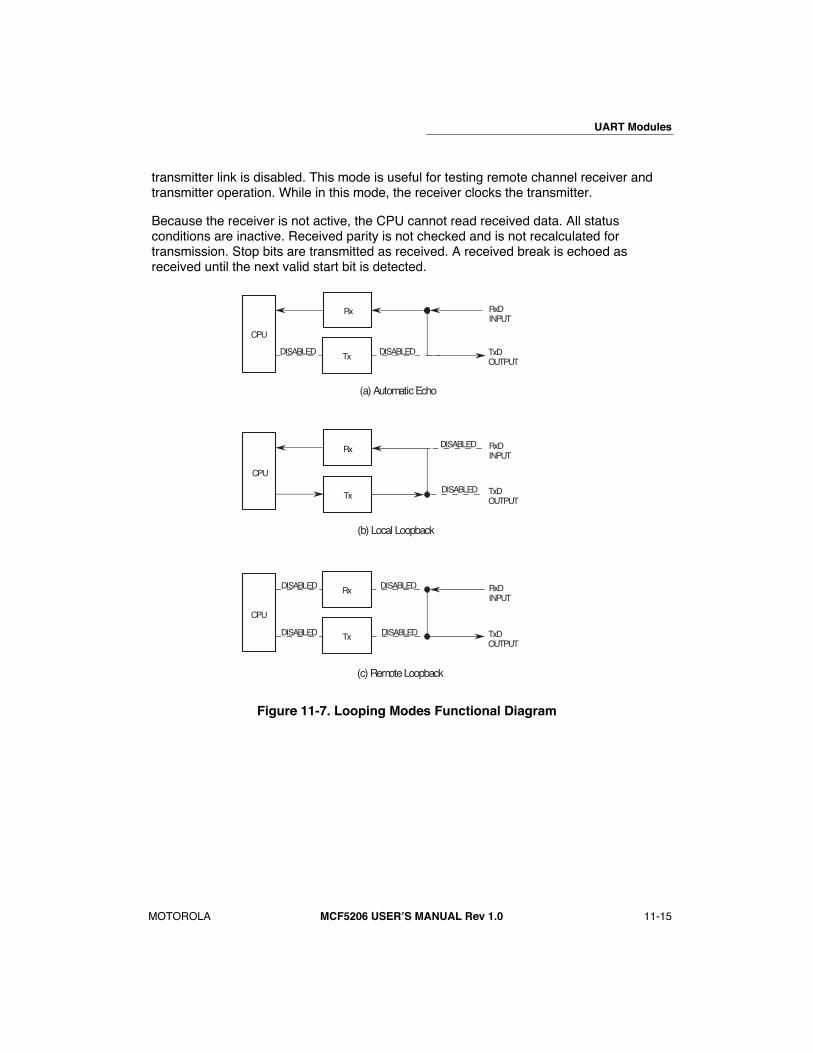
UART Modules
MOTOROLA
MCF5206 USERÕS MANUAL Rev 1.0
11-15
transmitter link is disabled. This mode is useful for testing remote channel receiver and transmitter operation. While in this mode, the receiver clocks the transmitter.
Because the receiver is not active, the CPU cannot read received data. All status conditions are inactive.
Received parity is not checked and is not recalculated for transmission. Stop bits are transmitted as received. A received break is echoed as received until the next valid start bit is detected.
Figure 11-7. Looping Modes Functional Diagram
(a) Automatic Echo
(b) Local Loopback
(c) Remote Loopback
DISABLED
DISABLED
DISABLED
DISABLED
Rx
Tx
Rx
Tx
Rx
Tx TxDOUTPUT
RxDINPUT
RxDINPUT
RxDINPUT
TxDOUTPUT
TxDOUTPUT
DISABLED
DISABLED
CPU
CPU
CPU
DISABLED
DISABLED

UART Modules
11-16
MCF5206 USERÕS MANUAL Rev 1.0
MOTOROLA
11.3.5 Multidrop Mode
You can program the UART to operate in a wakeup mode for multidrop or multiprocessor applications. Functional timing information for the multidrop mode is shown in Figure 11-8. You select the mode by setting bits 3 and 4 in UART mode register 1 (UMR1). This mode of operation connects the master station to several slave stations (maximum of 256). In this mode, the master transmits an address character followed by a block of data characters targeted for one of the slave stations. The slave stations channel receivers are disabled; however, they continuously monitor the data stream sent out by the master station. When the master sends an address character, the slave receiver channel notifies its respective CPU by setting the RxRDY bit in the USR and generating an interrupt (if programmed to do so). Each slave station CPU then compares the received address to its station address and enables its receiver if it wants to receive the subsequent data characters or block of data from the master station. Slave stations not addressed continue to monitor the data stream for the next address character. Data fields in the data stream are separated by an address character. After a slave receives a block of data, the slave station CPU disables the receiver and reinitiates the process.
A transmitted character from the master station consists of a start bit, a programmed number of data bits, an address/data (A/D) bit flag, and a programmed number of stop bits. The A/D bit identifies the type of character being transmitted to the slave station. The character is interpreted as an address character if the A/D bit is set or as a data character if the A/D bit is cleared. You select the polarity of the A/D bit by programming bit 2 of UMR1. You should also program UMR1 before enabling the transmitter and loading the corresponding data bits into the transmit buffer.
In multidrop mode, the receiver continuously monitors the received data stream, regardless of whether it is enabled or disabled. If the receiver is disabled, it sets the RxRDY bit and loads the character into the receiver holding register FIFO stack, provided the received A/D bit is a one (address tag). The character is discarded if the received A/D bit is a zero (data tag). If the receiver is enabled, all received characters are transferred to the CPU via the receiver holding register stack during read operations.
In either case, the data bits are loaded into the data portion of the stack while the A/D bit is loaded into the status portion of the stack normally used for a parity error (USR bit 5). Framing error, overrun error, and break detection operate normally. The A/D bit takes the place of the parity bit; therefore, parity is neither calculated nor checked. Messages in this mode can still contain error detection and correction information. One way to provide error detection, if 8-bit characters are not required, is to use software to calculate parity and append it to the 5-, 6-, or 7-bit character.
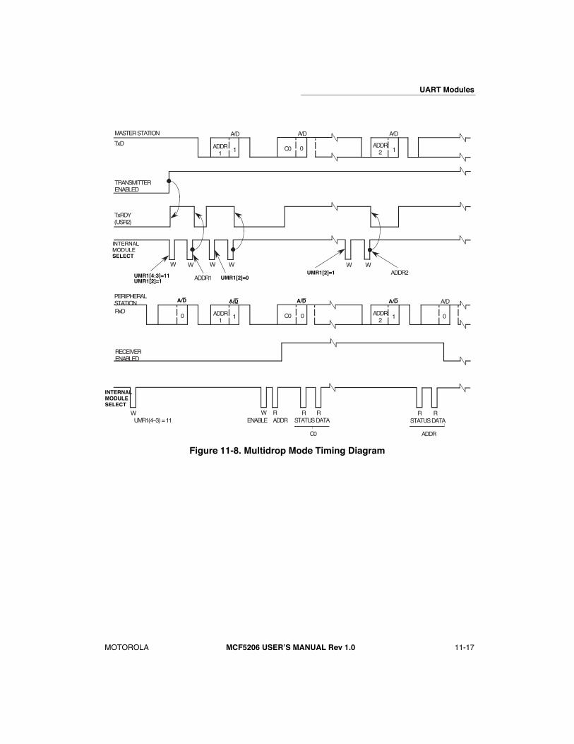
UART Modules
MOTOROLA
MCF5206 USERÕS MANUAL Rev 1.0
11-17
Figure 11-8. Multidrop Mode Timing Diagram
STATUS DATA STATUS DATA
1 0C0 1ADDR1
ADDR2
A/D A/D A/DMASTER STATION
1 0C0 10 ADDR1
ADDR2
A/D A/D A/D A/D A/DPERIPHERALSTATION
UMR1(2) = 1W W W W W W
UMR1(2) = 0ADDR2
ADDR1UMR1(4:3) = 11UMR1(2) = 1
0
UMR1(4Ð3) = 11 ADDRW R R R R R
C0 ADDR
RECEIVER ENABLED
RxD
CS
TxD
TRANSMITTER ENABLED
TxRDY(USR2)
CS
WENABLE
INTERNALMODULESELECT
INTERNALMODULESELECT
UMR1[4:3]=11UMR1[2]=1
UMR1[2]=0UMR1[2]=1
A/D A/D A/D A/D
UART Modules
11-18
MCF5206 USERÕS MANUAL Rev 1.0
MOTOROLA
11.3.6 Bus Operation
This subsection describes the operation of the bus during read, write, and interrupt- acknowledge cycles to the UART module. All UART module registers must be accessed as bytes.
11.3.6.1 READ CYCLES.
The CPU with zero wait states accesses the UART module because the MCF5206 system clock is also used for the UART module. The UART module responds to reads with byte data on D[7:0]. Reserved registers return logic zero during reads.
11.3.6.2 WRITE CYCLES.
The CPU with zero wait states accesses the UART module. The UART module accepts write data on D[7:0]. Write cycles to read-only registers and reserved registers complete in a normal manner without exception processing; however, the data is ignored.
11.3.6.3 INTERRUPT ACKNOWLEDGE CYCLES.
The UART module can arbitrate for interrupt servicing and supply the interrupt vector when it has successfully won arbitration. The vector number must be provided if interrupt servicing is necessary; thus, the interrupt vector register (UIVR) must be initialized.
The interrupt vector number generated by the IVR is used if the autovector is not enabled in the SIM Interrupt Control Register (ICR). If the UIVR is not initialized and the ICR is not programmed for autovector, a spurious interrupt exception is taken if interrupts are generated. This works in conjunction with the MCF5206 interrupt controller, which allows a programmable Interrupt Priority Level (IPL) for the interrupt.
11.4 REGISTER DESCRIPTION AND PROGRAMMING
This subsection contains a detailed description of each register and its specific function as well as flowcharts of basic UART module programming.
11.4.1 Register Description
Writing control bytes into the appropriate registers controls the UART operation. A list of UART module registers and their associated addresses is shown in Table 11-2.
NOTE
All UART module registers are accessible only as bytes. Youshould change the contents of the mode registers (UMR1 andUMR2), clock-select register (UCSR), and the auxiliary controlregister (UACR) bit 7 only after the receiver/transmitter isissued a software RESET commandÑi.e., channel operationmust be disabled. You should be careful if the registercontents are changed during receiver/transmitter operationsas unpredictable results can occur.
For the registers discussed in the following pages, the numbers above the register description represent the bit position in the register. The register description contains the
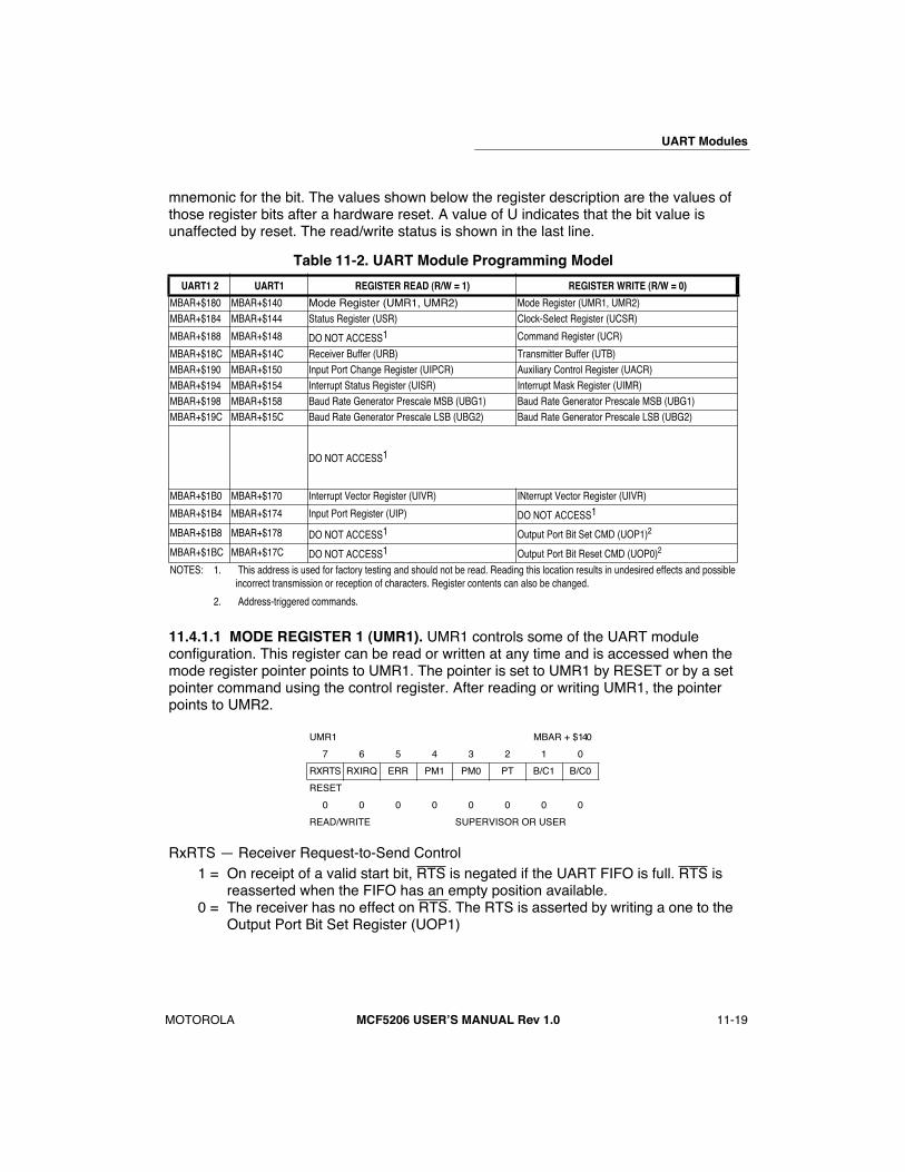
UART Modules
MOTOROLA
MCF5206 USERÕS MANUAL Rev 1.0
11-19
mnemonic for the bit. The values shown below the register description are the values of those register bits after a hardware reset. A value of U indicates that the bit value is unaffected by reset. The read/write status is shown in the last line.
11.4.1.1 MODE REGISTER 1 (UMR1). UMR1 controls some of the UART module configuration. This register can be read or written at any time and is accessed when the mode register pointer points to UMR1. The pointer is set to UMR1 by RESET or by a set pointer command using the control register. After reading or writing UMR1, the pointer points to UMR2.
RxRTS Ñ Receiver Request-to-Send Control1 = On receipt of a valid start bit, RTS is negated if the UART FIFO is full. RTS is
reasserted when the FIFO has an empty position available.0 = The receiver has no effect on RTS. The RTS is asserted by writing a one to the
Output Port Bit Set Register (UOP1)
Table 11-2. UART Module Programming Model
UART1 2 UART1 REGISTER READ (R/W = 1) REGISTER WRITE (R/W = 0)
MBAR+$180 MBAR+$140 Mode Register (UMR1, UMR2) Mode Register (UMR1, UMR2)MBAR+$184 MBAR+$144 Status Register (USR) Clock-Select Register (UCSR)
MBAR+$188 MBAR+$148 DO NOT ACCESS1 Command Register (UCR)
MBAR+$18C MBAR+$14C Receiver Buffer (URB) Transmitter Buffer (UTB)MBAR+$190 MBAR+$150 Input Port Change Register (UIPCR) Auxiliary Control Register (UACR)MBAR+$194 MBAR+$154 Interrupt Status Register (UISR) Interrupt Mask Register (UIMR)MBAR+$198 MBAR+$158 Baud Rate Generator Prescale MSB (UBG1) Baud Rate Generator Prescale MSB (UBG1)MBAR+$19C MBAR+$15C Baud Rate Generator Prescale LSB (UBG2) Baud Rate Generator Prescale LSB (UBG2)
DO NOT ACCESS1
MBAR+$1B0 MBAR+$170 Interrupt Vector Register (UIVR) INterrupt Vector Register (UIVR)
MBAR+$1B4 MBAR+$174 Input Port Register (UIP) DO NOT ACCESS1
MBAR+$1B8 MBAR+$178 DO NOT ACCESS1 Output Port Bit Set CMD (UOP1)2
MBAR+$1BC MBAR+$17C DO NOT ACCESS1 Output Port Bit Reset CMD (UOP0)2
NOTES: 1. This address is used for factory testing and should not be read. Reading this location results in undesired effects and possible incorrect transmission or reception of characters. Register contents can also be changed.
2. Address-triggered commands.
UMR1 MBAR + $140
7 6 5 4 3 2 1 0
RXRTS RXIRQ ERR PM1 PM0 PT B/C1 B/C0
RESET
0 0 0 0 0 0 0 0
READ/WRITE SUPERVISOR OR USER

UART Modules
11-20 MCF5206 USERÕS MANUAL Rev 1.0 MOTOROLA
You can use this feature for flow control to prevent overrun in the receiver by using the RTS output to control the CTS input of the transmitting device. If both the receiver and transmitter are programmed for RTS control, RTS control is disabled for both because such a configuration is incorrect. See Section 11.4.1.2 Mode Register 2 (UMR2) for information on programming the transmitter RTS control. On UART 2, RTS is muxed.
RxIRQ Ñ Receiver Interrupt Select1 = FFULL is the source that generates IRQ0 = RxRDY is the source that generates IRQ
ERR Ñ Error ModeThis bit controls the meaning of the three FIFO status bits (RB, FE, and PE) in the USR.
1 = Block modeÑThe values in the channel USR are the accumulation (i.e., the logical OR) of the status for all characters coming to the top of the FIFO since the last reset error status command for the channel was issued. Refer to Section 11.4.1.5 Command Register (UCR) for more information on UART module commands.
0 = Character modeÑThe values in the channel USR reflect the status of the character at the top of the FIFO.
NOTE
You must use ERR = 0 to obtain the correct A/D flaginformation when in multidrop mode.
PM1ÐPM0 Ñ Parity ModeThese bits encode the type of parity used for the channel (see Table 11-3). The parity bit is added to the transmitted character and the receiver performs a parity check on incoming data. These bits can alternatively select multidrop mode for the channel.
PT Ñ Parity TypeThis bit selects the parity type if parity is programmed by the parity mode bits; if multidrop mode is selected, it configures the transmitter for data character transmission or address character transmission. Table 11-3 lists the parity mode and type or the multidrop mode for each combination of the parity mode and the parity type bits.
Table 11-3. PMx and PT Control Bits
PM1 PM0 PARITY MODE PT PARITY TYPE
0 0 With Parity 0 Even Parity0 0 With Parity 1 Odd Parity0 1 Force Parity 0 Low Parity0 1 Force Parity 1 High Parity1 0 No Parity X No Parity1 1 Multidrop Mode 0 Data Character1 1 Multidrop Mode 1 Address Character
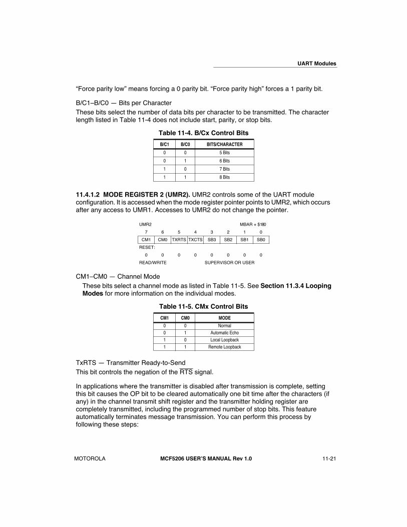
UART Modules
MOTOROLA MCF5206 USERÕS MANUAL Rev 1.0 11-21
ÒForce parity lowÓ means forcing a 0 parity bit. ÒForce parity highÓ forces a 1 parity bit.
B/C1ÐB/C0 Ñ Bits per CharacterThese bits select the number of data bits per character to be transmitted. The character length listed in Table 11-4 does not include start, parity, or stop bits.
11.4.1.2 MODE REGISTER 2 (UMR2). UMR2 controls some of the UART module configuration. It is accessed when the mode register pointer points to UMR2, which occurs after any access to UMR1. Accesses to UMR2 do not change the pointer.
CM1ÐCM0 Ñ Channel ModeThese bits select a channel mode as listed in Table 11-5. See Section 11.3.4 LoopingModes for more information on the individual modes.
TxRTS Ñ Transmitter Ready-to-SendThis bit controls the negation of the RTS signal.
In applications where the transmitter is disabled after transmission is complete, setting this bit causes the OP bit to be cleared automatically one bit time after the characters (if any) in the channel transmit shift register and the transmitter holding register are completely transmitted, including the programmed number of stop bits. This feature automatically terminates message transmission. You can perform this process by following these steps:
Table 11-4. B/Cx Control Bits
B/C1 B/C0 BITS/CHARACTER
0 0 5 Bits
0 1 6 Bits
1 0 7 Bits
1 1 8 Bits
UMR2 MBAR + $180
7 6 5 4 3 2 1 0
CM1 CM0 TXRTS TXCTS SB3 SB2 SB1 SB0
RESET:
0 0 0 0 0 0 0 0
READ/WRITE SUPERVISOR OR USER
Table 11-5. CMx Control Bits
CM1 CM0 MODE
0 0 Normal0 1 Automatic Echo1 0 Local Loopback1 1 Remote Loopback

UART Modules
11-22 MCF5206 USERÕS MANUAL Rev 1.0 MOTOROLA
1. Program the UART for the automatic-reset mode: UMR2[5]=1
2. Enable the transmitter
3. Assert the transmitter request-to send control: UOP1[0]=1
4. Send the message
5. Disable the transmitter after the TxRDY bit but not the TxEMP bit in the USR becomes asserted.
The last character is transmitted and the UOP0[0] bit is set causing the transmitter request-to-send control to be negated.
If both the receiver and the transmitter in the same channel are programmed for RTS control, RTS control is disabled for both because of this incorrect configuration.
1 = If both TxRDY and TXEMP bits in the UART Status Register (USR) are set, there is no change on RTS. For TXRTS to be set to 1 in this condition, you must set the UART Output Port Set Data Register (UOP1).
0 = The transmitter has no effect on RTS.
TxCTS Ñ Transmitter Clear-to-Send1 = Enables clear-to-send operation. The transmitter checks the state of the CTS
input each time it is ready to send a character. If CTS is asserted, the character is transmitted. If CTS is negated, the channel TxD remains in the high state (mark condition) and the transmission is delayed until CTS is asserted. Changes in CTS while a character is being transmitted do not affect transmission of that character.
0 = The CTS has no effect on the transmitter.
SB3ÐSB0 Ñ Stop-Bit Length ControlThese bits select the length of the stop bit appended to the transmitted character as listed in Table 11-6. Stop-bit lengths of 9/16 to two bits, in increments of 1/16 bit, are programmable for character lengths of six, seven, and eight bits. For a character length of five bits, 1-1/16 to two bits are programmable in increments of 1/16 bit. In all cases, the receiver only checks for a high condition at the center of the first stop-bit positionÑi.e., one bit time after the last data bit or after the parity bit, if parity is enabled.
If an external 1´ clock is used for the transmitter, UMR2 bit 3 = 0 selects one stop bit, and UMR2 bit 3 = 1 selects two stop bits for transmission.
Table 11-6. SBx Control Bits
SB3 SB2 SB1 SB0 LENGTH 6-8 BITS LENGTH 5 BITS
0 0 0 0 0.563 1.0630 0 0 1 0.625 1.1250 0 1 0 0.688 1.1880 0 1 1 0.750 1.250
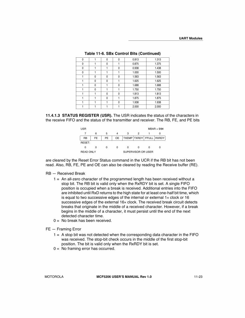
UART Modules
MOTOROLA MCF5206 USERÕS MANUAL Rev 1.0 11-23
11.4.1.3 STATUS REGISTER (USR). The USR indicates the status of the characters in the receive FIFO and the status of the transmitter and receiver. The RB, FE, and PE bits
are cleared by the Reset Error Status command in the UCR if the RB bit has not been read. Also, RB, FE, PE and OE can also be cleared by reading the Receive buffer (RE).
RB Ñ Received Break1 = An all-zero character of the programmed length has been received without a
stop bit. The RB bit is valid only when the RxRDY bit is set. A single FIFO position is occupied when a break is received. Additional entries into the FIFO are inhibited until RxD returns to the high state for at least one-half bit time, which is equal to two successive edges of the internal or external 1´ clock or 16 successive edges of the external 16´ clock. The received break circuit detects breaks that originate in the middle of a received character. However, if a break begins in the middle of a character, it must persist until the end of the next detected character time.
0 = No break has been received.
FE Ñ Framing Error1 = A stop bit was not detected when the corresponding data character in the FIFO
was received. The stop-bit check occurs in the middle of the first stop-bit position. The bit is valid only when the RxRDY bit is set.
0 = No framing error has occurred.
0 1 0 0 0.813 1.3130 1 0 1 0.875 1.3750 1 1 0 0.938 1.4380 1 1 1 1.000 1.5001 0 0 0 1.563 1.5631 0 0 1 1.625 1.6251 0 1 0 1.688 1.6881 0 1 1 1.750 1.7501 1 0 0 1.813 1.8131 1 0 1 1.875 1.8751 1 1 0 1.938 1.9381 1 1 1 2.000 2.000
USR MBAR + $184
7 6 5 4 3 2 1 0
RB FE PE OE TXEMP TXRDY FFULL RXRDY
RESET:
0 0 0 0 0 0 0 0
READ ONLY SUPERVISOR OR USER
Table 11-6. SBx Control Bits (Continued)

UART Modules
11-24 MCF5206 USERÕS MANUAL Rev 1.0 MOTOROLA
PE Ñ Parity Error1 = When the with-parity or force-parity mode is programmed in the UMR1, the
corresponding character in the FIFO was received with incorrect parity. When the multidrop mode is programmed, this bit stores the received A/D bit. This bit is valid only when the RxRDY bit is set.
0 = No parity error has occurred.
OE Ñ Overrun Error1 = One or more characters in the received data stream have been lost. This bit is
set on receipt of a new character when the FIFO is full and a character is already in the shift register waiting for an empty FIFO position. When this occurs, the character in the receiver-shift register and its break-detect, framing-error status, and parity error, if any, are lost. The reset-error status command in the UCR clears this bit.
0 = No overrun has occurred.

UART Modules
MOTOROLA MCF5206 USERÕS MANUAL Rev 1.0 11-25
TxEMP Ñ Transmitter Empty1 = The transmitter has underrun (both the transmitter holding register and
transmitter shift registers are empty). This bit is set after transmission of the last stop bit of a character if there are no characters in the transmitter-holding register awaiting transmission.
0 = The transmitter buffer is not empty. Either a character is currently being shifted out or the transmitter is disabled. You can enable/disable the transmitter by programming the TCx bits in the UCR.
TxRDY Ñ Transmitter Ready1 = The transmitter-holding register is empty and ready to be loaded with a
character. This bit is set when the character is transferred to the transmitter shift register. This bit is also set when the transmitter is first enabled. Characters loaded into the transmitter holding register while the transmitter is disabled are not transmitted.
0 = The CPU has loaded the transmitter-holding register or the transmitter is disabled.
FFULL Ñ FIFO Full1 = Three characters have been received and are waiting in the receiver buffer
FIFO.0 = The FIFO is not full but can contain as many as two unread characters.
RxRDY Ñ Receiver Ready1 = One or more characters have been received and are waiting in the receiver
buffer FIFO. 0 = The CPU has read the receiver buffer and no characters remain in the FIFO after
this read.
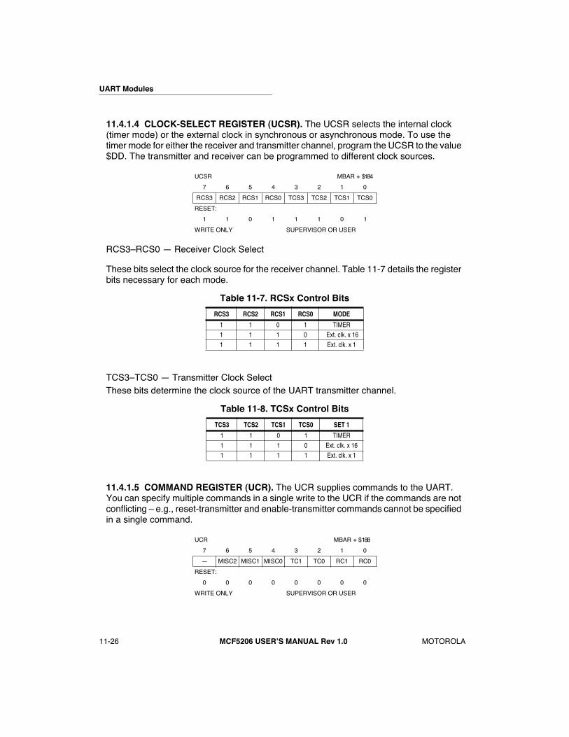
UART Modules
11-26 MCF5206 USERÕS MANUAL Rev 1.0 MOTOROLA
11.4.1.4 CLOCK-SELECT REGISTER (UCSR). The UCSR selects the internal clock (timer mode) or the external clock in synchronous or asynchronous mode. To use the timer mode for either the receiver and transmitter channel, program the UCSR to the value $DD. The transmitter and receiver can be programmed to different clock sources.
RCS3ÐRCS0 Ñ Receiver Clock Select
These bits select the clock source for the receiver channel. Table 11-7 details the register bits necessary for each mode.
TCS3ÐTCS0 Ñ Transmitter Clock SelectThese bits determine the clock source of the UART transmitter channel.
11.4.1.5 COMMAND REGISTER (UCR). The UCR supplies commands to the UART. You can specify multiple commands in a single write to the UCR if the commands are not conflicting Ð e.g., reset-transmitter and enable-transmitter commands cannot be specified in a single command.
UCSR MBAR + $184
7 6 5 4 3 2 1 0
RCS3 RCS2 RCS1 RCS0 TCS3 TCS2 TCS1 TCS0
RESET:
1 1 0 1 1 1 0 1
WRITE ONLY SUPERVISOR OR USER
Table 11-7. RCSx Control Bits
RCS3 RCS2 RCS1 RCS0 MODE
1 1 0 1 TIMER1 1 1 0 Ext. clk. x 161 1 1 1 Ext. clk. x 1
Table 11-8. TCSx Control Bits
TCS3 TCS2 TCS1 TCS0 SET 1
1 1 0 1 TIMER1 1 1 0 Ext. clk. x 161 1 1 1 Ext. clk. x 1
UCR MBAR + $188
7 6 5 4 3 2 1 0
Ñ MISC2 MISC1 MISC0 TC1 TC0 RC1 RC0
RESET:
0 0 0 0 0 0 0 0
WRITE ONLY SUPERVISOR OR USER

UART Modules
MOTOROLA MCF5206 USERÕS MANUAL Rev 1.0 11-27
MISC3ÐMISC0 Ñ Miscellaneous CommandsThese bits select a single command as listed in Table 11-9.
The commands are described as follows:
Reset Mode Register Pointer
The reset mode register pointer command causes the mode register pointer to point to UMR1.
Reset Receiver
The reset receiver command resets the receiver. The receiver is immediately disabled, the FFULL and RxRDY bits in the USR are cleared, and the receiver FIFO pointer is reinitialized. All other registers are unaltered. Use this command instead of the receiver-disable command whenever the receiver configuration is changed (it places the receiver in a known state).
Reset Transmitter
The reset transmitter command resets the transmitter. The transmitter is immediately disabled and the TxEMP and TxRDY bits in the USR are cleared. All other registers are unaltered. Use this command instead of the transmitter-disable command whenever the transmitter configuration is changed (it places the transmitter in a known state).
Reset Error Status
The reset error status command clears the RB, FE, PE, and OE bits in the USR. This command is also used in the block mode to clear all error bits after a data block is received.
Reset Break-Change Interrupt
The reset break-change interrupt command clears the delta break (DBx) bit in the UISR.
Table 11-9. MISCx Control Bits
MISC2 MISC1 MISC0 COMMAND
0 0 0 No Command0 0 1 Reset Mode Register Pointer0 1 0 Reset Receiver0 1 1 Reset Transmitter1 0 0 Reset Error Status1 0 1 Reset Break-Change Interrupt1 1 0 Start Break1 1 1 Stop Break
UART Modules
11-28 MCF5206 USERÕS MANUAL Rev 1.0 MOTOROLA
Start Break
The start break command forces TxD low. If the transmitter is empty, the start of the break conditions can be delayed by as much as two bit times. If the transmitter is active, the break begins when transmission of the character is complete. If a character is in the transmitter shift register, the start of the break is delayed until the character is transmitted. If the transmitter holding register has a character, that character is transmitted before the break. The transmitter must be enabled for this command to be accepted. The state of the CTS input is ignored for this command.
Stop Break
The stop break command causes TxD to go high (mark) within two bit times. Characters stored in the transmitter buffer, if any, are transmitted.
TC1ÐTC0 Ñ Transmitter CommandsThese bits select a single command as listed in Table 11-10.
The definitions of the transmitter command options are as follows:
No Action Taken
The ÔÔno action takenÕÕ command causes the transmitter to stay in its current mode. If the transmitter is enabled, it remains enabled; if disabled, it remains disabled.
Transmitter Enable
The ÔÔtransmitter enableÕÕ command enables operation of the channel's transmitter. The TxEMP and TxRDY bits in the USR are also set. If the transmitter is already enabled, this command has no effect.
Transmitter Disable
The ÔÔtransmitter disableÕÕ command terminates transmitter operation and clears the TxEMP and TxRDY bits in the USR. However, if a character is being transmitted when the transmitter is disabled, the transmission of the character is completed before the transmitter becomes inactive. If the transmitter is already disabled, this command has no effect.
Table 11-10. TCx Control Bits
TC1 TC0 COMMAND
0 0 No Action Taken0 1 Transmitter Enable1 0 Transmitter Disable1 1 Do Not Use

UART Modules
MOTOROLA MCF5206 USERÕS MANUAL Rev 1.0 11-29
Do Not Use
Do not use this bit combination because the result is indeterminate.
RC1ÐRC0 Ñ Receiver CommandsThese bits select a single command as listed in Table 11-11.
No Action Taken
The ÔÔno action takenÕÕ command causes the receiver to stay in its current mode. If the receiver is enabled, it remains enabled; if disabled, it remains disabled.
Receiver Enable
The ÔÔreceiver enableÕÕ command enables operation of the channel's receiver. If the UART module is not in multidrop mode, this command also forces the receiver into the search-for-start-bit state. If the receiver is already enabled, this command has no effect.
Receiver Disable
The ÔÔreceiver disableÕÕ command immediately disables the receiver. Any character being received is lost. The command has no effect on the receiver status bits or any other control register. If the UART module is programmed to operate in the local loopback mode or multidrop mode, the receiver operates even though this command is selected. If the receiver is already disabled, this command has no effect.
Do Not UseDo not use this bit combination because the result is indeterminate.
11.4.1.6 RECEIVER BUFFER (URB). The receiver buffer contains three receiver-holding registers and a serial shift register. The RxD pin is connected to the serial shift register while the holding registers act as a FIFO. The CPU reads from the top of the stack
Table 11-11. RCx Control Bits
RC1 RC0 COMMAND
0 0 No Action Taken0 1 Receiver Enable1 0 Receiver Disable1 1 Do Not Use
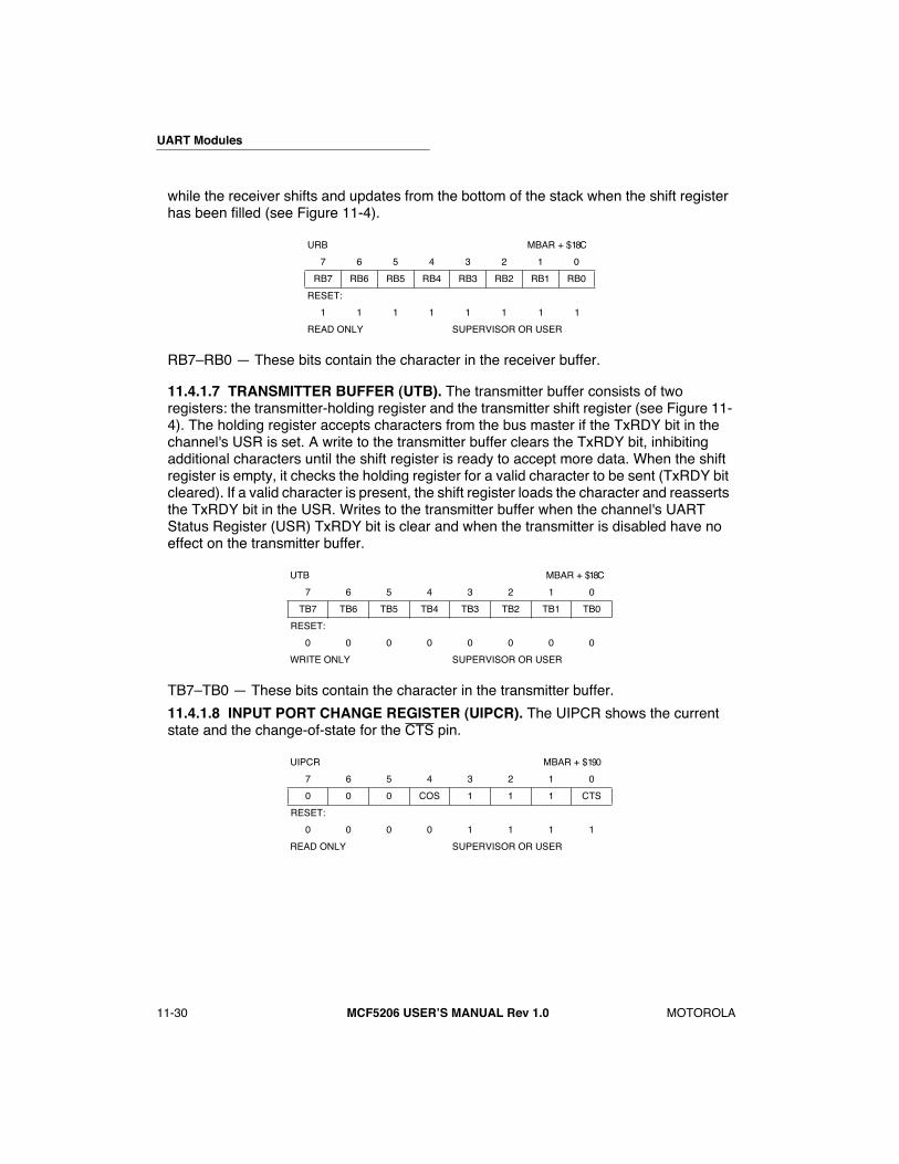
UART Modules
11-30 MCF5206 USERÕS MANUAL Rev 1.0 MOTOROLA
while the receiver shifts and updates from the bottom of the stack when the shift register has been filled (see Figure 11-4).
RB7ÐRB0 Ñ These bits contain the character in the receiver buffer.
11.4.1.7 TRANSMITTER BUFFER (UTB). The transmitter buffer consists of two registers: the transmitter-holding register and the transmitter shift register (see Figure 11-4). The holding register accepts characters from the bus master if the TxRDY bit in the channel's USR is set. A write to the transmitter buffer clears the TxRDY bit, inhibiting additional characters until the shift register is ready to accept more data. When the shift register is empty, it checks the holding register for a valid character to be sent (TxRDY bit cleared). If a valid character is present, the shift register loads the character and reasserts the TxRDY bit in the USR. Writes to the transmitter buffer when the channel's UART Status Register (USR) TxRDY bit is clear and when the transmitter is disabled have no effect on the transmitter buffer.
TB7ÐTB0 Ñ These bits contain the character in the transmitter buffer.
11.4.1.8 INPUT PORT CHANGE REGISTER (UIPCR). The UIPCR shows the current state and the change-of-state for the CTS pin.
URB MBAR + $18C
7 6 5 4 3 2 1 0
RB7 RB6 RB5 RB4 RB3 RB2 RB1 RB0
RESET:
1 1 1 1 1 1 1 1
READ ONLY SUPERVISOR OR USER
UTB MBAR + $18C
7 6 5 4 3 2 1 0
TB7 TB6 TB5 TB4 TB3 TB2 TB1 TB0
RESET:
0 0 0 0 0 0 0 0
WRITE ONLY SUPERVISOR OR USER
UIPCR MBAR + $190
7 6 5 4 3 2 1 0
0 0 0 COS 1 1 1 CTS
RESET:
0 0 0 0 1 1 1 1
READ ONLY SUPERVISOR OR USER
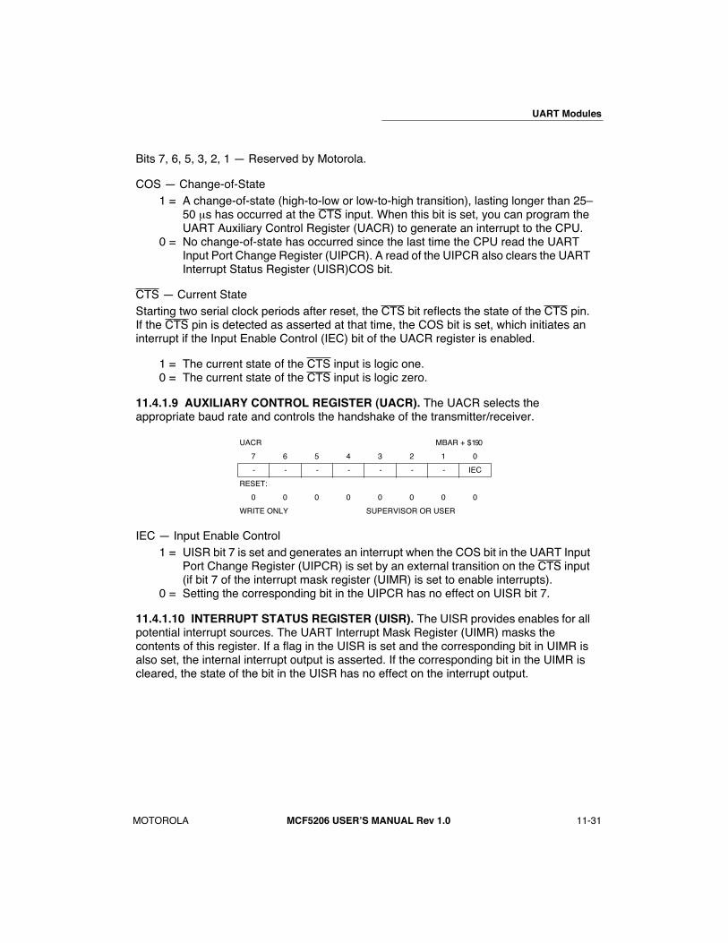
UART Modules
MOTOROLA MCF5206 USERÕS MANUAL Rev 1.0 11-31
Bits 7, 6, 5, 3, 2, 1 Ñ Reserved by Motorola.
COS Ñ Change-of-State1 = A change-of-state (high-to-low or low-to-high transition), lasting longer than 25Ð
50 ms has occurred at the CTS input. When this bit is set, you can program the UART Auxiliary Control Register (UACR) to generate an interrupt to the CPU.
0 = No change-of-state has occurred since the last time the CPU read the UART Input Port Change Register (UIPCR). A read of the UIPCR also clears the UART Interrupt Status Register (UISR)COS bit.
CTS Ñ Current StateStarting two serial clock periods after reset, the CTS bit reflects the state of the CTS pin. If the CTS pin is detected as asserted at that time, the COS bit is set, which initiates an interrupt if the Input Enable Control (IEC) bit of the UACR register is enabled.
1 = The current state of the CTS input is logic one.0 = The current state of the CTS input is logic zero.
11.4.1.9 AUXILIARY CONTROL REGISTER (UACR). The UACR selects the appropriate baud rate and controls the handshake of the transmitter/receiver.
IEC Ñ Input Enable Control1 = UISR bit 7 is set and generates an interrupt when the COS bit in the UART Input
Port Change Register (UIPCR) is set by an external transition on the CTS input (if bit 7 of the interrupt mask register (UIMR) is set to enable interrupts).
0 = Setting the corresponding bit in the UIPCR has no effect on UISR bit 7.
11.4.1.10 INTERRUPT STATUS REGISTER (UISR). The UISR provides enables for all potential interrupt sources. The UART Interrupt Mask Register (UIMR) masks the contents of this register. If a flag in the UISR is set and the corresponding bit in UIMR is also set, the internal interrupt output is asserted. If the corresponding bit in the UIMR is cleared, the state of the bit in the UISR has no effect on the interrupt output.
UACR MBAR + $190
7 6 5 4 3 2 1 0
- - - - - - - IEC
RESET:
0 0 0 0 0 0 0 0
WRITE ONLY SUPERVISOR OR USER
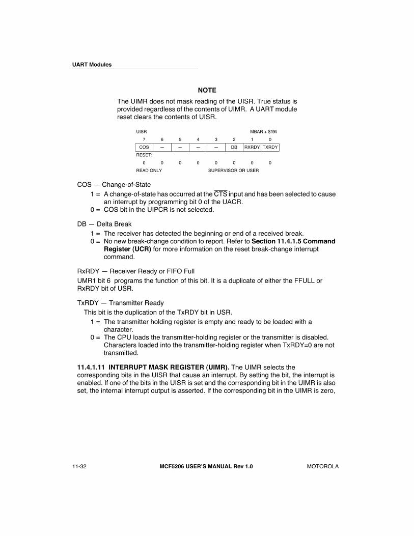
UART Modules
11-32 MCF5206 USERÕS MANUAL Rev 1.0 MOTOROLA
NOTE
The UIMR does not mask reading of the UISR. True status isprovided regardless of the contents of UIMR. A UART modulereset clears the contents of UISR.
COS Ñ Change-of-State1 = A change-of-state has occurred at the CTS input and has been selected to cause
an interrupt by programming bit 0 of the UACR.0 = COS bit in the UIPCR is not selected.
DB Ñ Delta Break 1 = The receiver has detected the beginning or end of a received break.0 = No new break-change condition to report. Refer to Section 11.4.1.5 Command
Register (UCR) for more information on the reset break-change interrupt command.
RxRDY Ñ Receiver Ready or FIFO FullUMR1 bit 6 programs the function of this bit. It is a duplicate of either the FFULL or RxRDY bit of USR.
TxRDY Ñ Transmitter ReadyThis bit is the duplication of the TxRDY bit in USR.
1 = The transmitter holding register is empty and ready to be loaded with a character.
0 = The CPU loads the transmitter-holding register or the transmitter is disabled. Characters loaded into the transmitter-holding register when TxRDY=0 are not transmitted.
11.4.1.11 INTERRUPT MASK REGISTER (UIMR). The UIMR selects the corresponding bits in the UISR that cause an interrupt. By setting the bit, the interrupt is enabled. If one of the bits in the UISR is set and the corresponding bit in the UIMR is also set, the internal interrupt output is asserted. If the corresponding bit in the UIMR is zero,
UISR MBAR + $194
7 6 5 4 3 2 1 0
COS Ñ Ñ Ñ Ñ DB RXRDY TXRDY
RESET:
0 0 0 0 0 0 0 0
READ ONLY SUPERVISOR OR USER
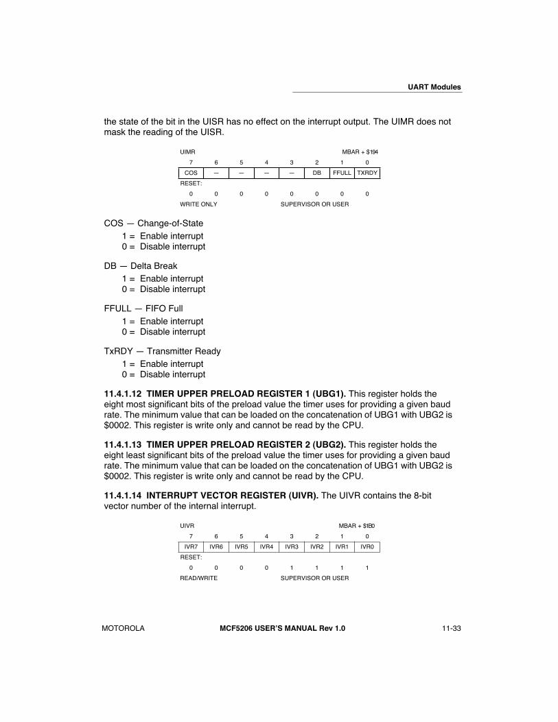
UART Modules
MOTOROLA MCF5206 USERÕS MANUAL Rev 1.0 11-33
the state of the bit in the UISR has no effect on the interrupt output. The UIMR does not mask the reading of the UISR.
COS Ñ Change-of-State1 = Enable interrupt0 = Disable interrupt
DB Ñ Delta Break1 = Enable interrupt0 = Disable interrupt
FFULL Ñ FIFO Full1 = Enable interrupt0 = Disable interrupt
TxRDY Ñ Transmitter Ready1 = Enable interrupt0 = Disable interrupt
11.4.1.12 TIMER UPPER PRELOAD REGISTER 1 (UBG1). This register holds the eight most significant bits of the preload value the timer uses for providing a given baud rate. The minimum value that can be loaded on the concatenation of UBG1 with UBG2 is $0002. This register is write only and cannot be read by the CPU.
11.4.1.13 TIMER UPPER PRELOAD REGISTER 2 (UBG2). This register holds the eight least significant bits of the preload value the timer uses for providing a given baud rate. The minimum value that can be loaded on the concatenation of UBG1 with UBG2 is $0002. This register is write only and cannot be read by the CPU.
11.4.1.14 INTERRUPT VECTOR REGISTER (UIVR). The UIVR contains the 8-bit vector number of the internal interrupt.
UIMR MBAR + $194
7 6 5 4 3 2 1 0
COS Ñ Ñ Ñ Ñ DB FFULL TXRDY
RESET:
0 0 0 0 0 0 0 0
WRITE ONLY SUPERVISOR OR USER
UIVR MBAR + $1B0
7 6 5 4 3 2 1 0
IVR7 IVR6 IVR5 IVR4 IVR3 IVR2 IVR1 IVR0
RESET:
0 0 0 0 1 1 1 1
READ/WRITE SUPERVISOR OR USER
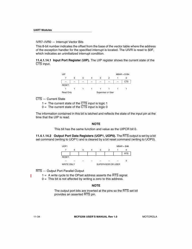
UART Modules
11-34 MCF5206 USERÕS MANUAL Rev 1.0 MOTOROLA
IVR7ÐIVR0 Ñ Interrupt Vector BitsThis 8-bit number indicates the offset from the base of the vector table where the address of the exception handler for the specified interrupt is located. The UIVR is reset to $0F, which indicates an uninitialized interrupt condition.
11.4.1.14.1 Input Port Register (UIP). The UIP register shows the current state of the CTS input.
CTS Ñ Current State1 = The current state of the CTS input is logic 10 = The current state of the CTS input is logic 0
The information contained in this bit is latched and reflects the state of the input pin at the time that the UIP is read.
NOTE
This bit has the same function and value as the UIPCR bit 0.
11.4.1.14.2 Output Port Data Registers (UOP1, UOP0). The RTS output is set by a bit set command (writing to UOP1) and is cleared by a bit reset command (writing to UOP0).
RTS Ñ Output Port Parallel Output1 = A write cycle to the OPset address asserts the RTS signal.0 = This bit is not affected by writing a zero to this address.
NOTE
The output port bits are inverted at the pins so the RTS set bitprovides an asserted RTS pin.
UIP MBAR + $1B4
7 6 5 4 3 2 1 0
Ñ Ñ Ñ Ñ Ñ Ñ Ñ CTS
RESET:
1 1 1 1 1 1 1 1
Read Only Supervisor or User
UOP1 MBAR + $148
7 6 5 4 3 2 1 0
RTS
RESET:
Ñ Ñ Ñ Ñ Ñ Ñ Ñ 0
WRITE ONLY SUPERVISOR OR USER
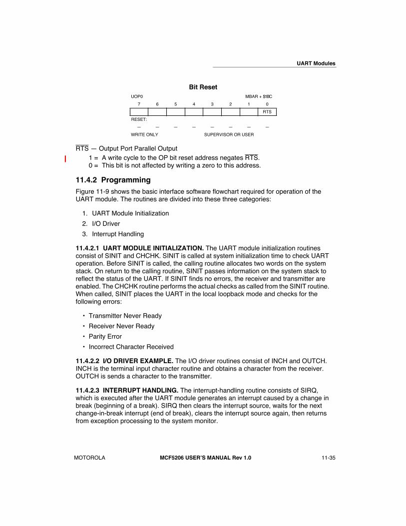
UART Modules
MOTOROLA MCF5206 USERÕS MANUAL Rev 1.0 11-35
Bit Reset
RTS Ñ Output Port Parallel Output1 = A write cycle to the OP bit reset address negates RTS.0 = This bit is not affected by writing a zero to this address.
11.4.2 Programming Figure 11-9 shows the basic interface software flowchart required for operation of the UART module. The routines are divided into these three categories:
1. UART Module Initialization
2. I/O Driver
3. Interrupt Handling
11.4.2.1 UART MODULE INITIALIZATION. The UART module initialization routines consist of SINIT and CHCHK. SINIT is called at system initialization time to check UART operation. Before SINIT is called, the calling routine allocates two words on the system stack. On return to the calling routine, SINIT passes information on the system stack to reflect the status of the UART. If SINIT finds no errors, the receiver and transmitter are enabled. The CHCHK routine performs the actual checks as called from the SINIT routine. When called, SINIT places the UART in the local loopback mode and checks for the following errors:
¥ Transmitter Never Ready
¥ Receiver Never Ready
¥ Parity Error
¥ Incorrect Character Received
11.4.2.2 I/O DRIVER EXAMPLE. The I/O driver routines consist of INCH and OUTCH. INCH is the terminal input character routine and obtains a character from the receiver. OUTCH is sends a character to the transmitter.
11.4.2.3 INTERRUPT HANDLING. The interrupt-handling routine consists of SIRQ, which is executed after the UART module generates an interrupt caused by a change in break (beginning of a break). SIRQ then clears the interrupt source, waits for the next change-in-break interrupt (end of break), clears the interrupt source again, then returns from exception processing to the system monitor.
UOP0 MBAR + $1BC
7 6 5 4 3 2 1 0
RTS
RESET:
Ñ Ñ Ñ Ñ Ñ Ñ Ñ Ñ
WRITE ONLY SUPERVISOR OR USER

UART Modules
11-36 MCF5206 USERÕS MANUAL Rev 1.0 MOTOROLA
11.5 UART MODULE INITIALIZATION SEQUENCE The following steps are required to properly initialize the UART module:
Command Register (UCR)
1. Reset the receiver and transmitter.
2. Program the vector number for a UART module interrupt. However, if the UART Interrupt Control Register (ICR_U1) is programmed to generate an autovector, the UART Interrupt Vector Register (UIVR) must be programmed with an autovector number.
Interrupt Mask Register (UIMR)
1. Enable the desired interrupt sources.
Auxiliary Control Register (UACR)
1. Initialize the Input Enable Control (IEC) bit.
2. Select timer mode and clock source, if necessary.
Clock Select Register (UCSR)
1. Select the receiver and transmitter clock. Use timer as source, if required.
Mode Register 1 (UMR1)
1. If required, program operation of Receiver Ready-to-Send (RxRTS Bit).
2. Select Receiver-Ready or FIFO-Full Notification (R/F Bit).
3. Select character or block-error mode (ERR Bit).
4. Select parity mode and type (PM and PT Bits).
5. Select number of bits per character (B/Cx Bits).
Mode Register 2 (UMR2)
1. Select the mode of operation (CMx bits).
2. If required, program operation of Transmitter Ready-to-Send (TxRTS Bit).
3. If required, program operation of Clear-to-Send (TxCTS Bit).
4. Select stop-bit length (SBx Bits).
Command Register (UCR)Enable the receiver and transmitter.

UART Modules
MOTOROLA MCF5206 USERÕS MANUAL Rev 1.0 11-37
SERIAL MODULE
INITIATE:
CHANNELINTERRUPTS
SAVE CHANNELSTATUS
ANYERRORS
?
ENABLE RECEIVER
ASSERT REQUEST TO SEND
RETURN
SINIT
CHK1
ENABLA
Y
N
SINITR
CALL CHCHK
ENABLE
Figure 11-9. UART Software Flowchart (1 of 5)
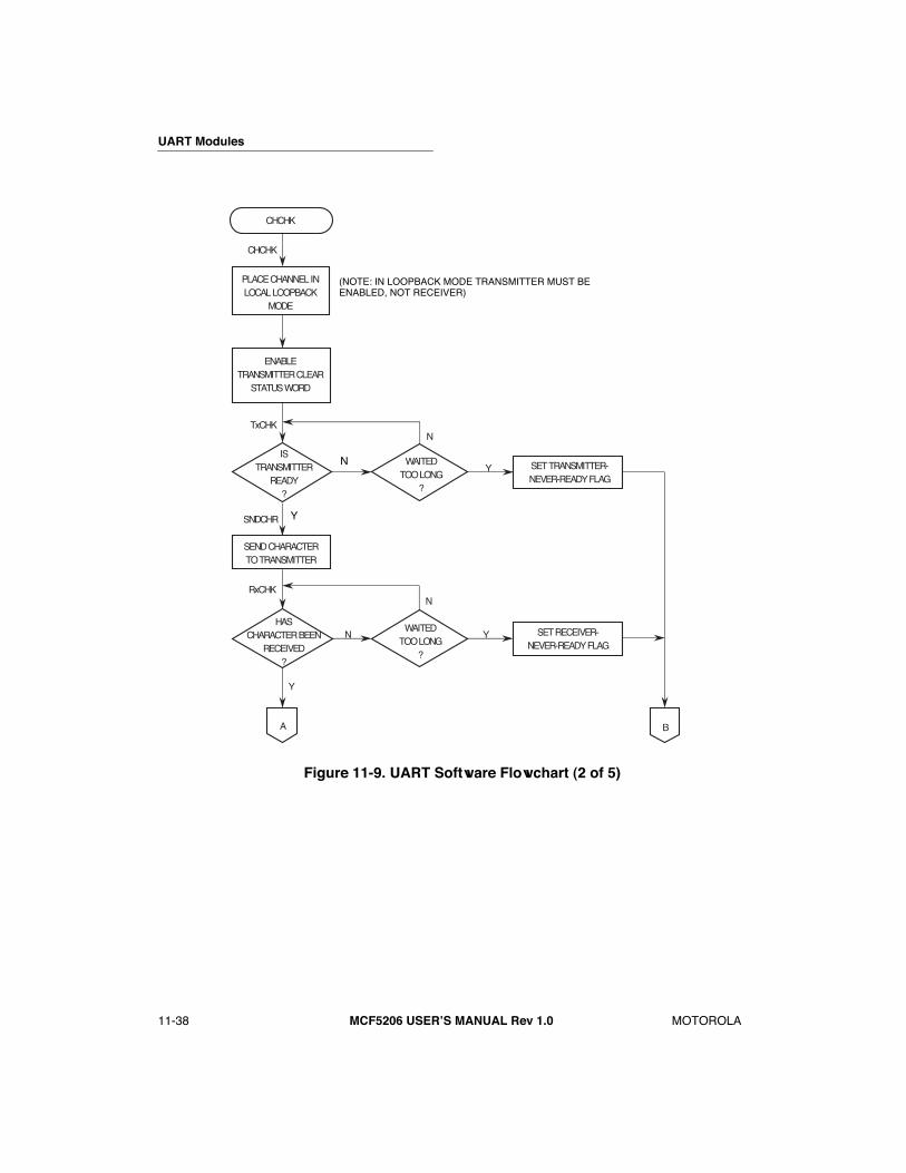
UART Modules
11-38 MCF5206 USERÕS MANUAL Rev 1.0 MOTOROLA
Y
N
CHCHK
PLACE CHANNEL INLOCAL LOOPBACK
MODE
ENABLE TRANSMITTER CLEAR
STATUS WORD
ISTRANSMITTER
READY?
WAITED TOO LONG
?
WAITED TOO LONG
?
N
Y
SEND CHARACTERTO TRANSMITTER
HAS CHARACTER BEEN
RECEIVED?
CHCHK
TxCHK
SNDCHR
RxCHKN
YN
SET TRANSMITTER- NEVER-READY FLAG
SET RECEIVER-NEVER-READY FLAG
A B
Y
N
Y
(NOTE: IN LOOPBACK MODE TRANSMITTER MUST BEENABLED, NOT RECEIVER)
Figure 11-9. UART Software Flowchart (2 of 5)

UART Modules
MOTOROLA MCF5206 USERÕS MANUAL Rev 1.0 11-39
B
Y
N
N
A
Y
A B
Y
N
RETURN
HAVEFRAMING ERROR
?
SET FRAMINGERROR FLAG
HAVEPARITY ERROR
?
SET PARITY ERROR FLAG
GET CHARACTERFROM RECEIVER
SAME AS TRANSMITTEDCHARACTER
?
SET INCORRECTCHARACTER FLAG
DISABLE TRANSMITTER
RESTORE TO ORIGINAL MODE
FRCHK RSTCHN
PRCHK
CHRCHK
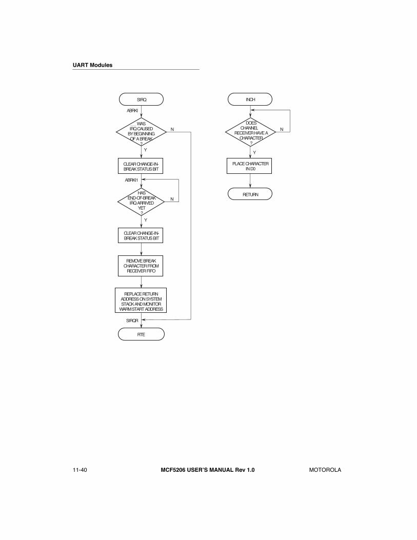
UART Modules
11-40 MCF5206 USERÕS MANUAL Rev 1.0 MOTOROLA
WASIRQ CAUSED
BY BEGINNINGOF A BREAK
?
CLEAR CHANGE-IN-BREAK STATUS BIT
HASEND-OF-BREAKIRQ ARRIVED
YET?
CLEAR CHANGE-IN- BREAK STATUS BIT
REMOVE BREAKCHARACTER FROM
RECEIVER FIFO
REPLACE RETURNADDRESS ON SYSTEMSTACK AND MONITOR
WARM START ADDRESS
RTE
SIRQR
N
Y
N
DOESCHANNEL A
RECEIVER HAVE A CHARACTER
?
PLACE CHARACTERIN D0
N
Y
ABRKI1
ABRKI
Y
INCH
RETURN
SIRQ

UART Modules
11-41 MCF5206 USERÕS MANUAL Rev 1.0 MOTOROLA
Figure 11-9. UART Software Flowchart (5 of 5)
OUTCH
N
Y
IS TRANSMITTER
READY?
SEND CHARACTERTO TRANSMITTER
RETURN

MOTOROLA
MCF5206 USERÕS MANUAL Rev 1.0
12-1
2
4
5
6
7
8
9
10
11
12
13
14
16
1
SECTION 12M-BUS MODULE
12.1 OVERVIEW
Motorola bus (M-Bus) is a two-wire, bidirectional serial bus that provides a simple, efficient method of data exchange between devices. It is compatible with the widely used I
2
C bus standard
1
. This two-wire bus minimizes the interconnection between devices.
This bus is suitable for applications requiring occasional communications over a short distance between many devices. The flexible M-Bus allows additional devices to be connected to the bus for expansion and system development.
The interface operates up to 100 kbps with maximum bus loading and timing.
The M-Bus system is a true multimaster bus including collision detection and arbitration that prevents data corruption if two or more masters attempt to control the bus simultaneously. This feature allows for complex applications with multiprocessor control. It can also be used for rapid testing and alignment of end products via external connections to an assembly line computer.
12.2 INTERFACE FEATURES
The M-Bus module has the following key features:
¥ Compatibility with I
2
C Bus standard
¥ Multimaster operation
¥ Software-programmable for one of 64 different serial clock frequencies
¥ Software-selectable acknowledge bit
¥ Interrupt-driven byte-by-byte data transfer
¥ Arbitration-lost interrupt with automatic mode switching from master to slave
¥ Calling address identification interrupt
¥ Start and stop signal generation/detection
¥ Repeated START signal generation
¥ Acknowledge bit generation/detection
¥ Bus-busy detection
1.
I
2
C-Bus is a proprietary Philips interface bus.
DATE: 9-2-98
REVISION NO.: 1.1
PAGES AFFECTED: SEE CHANGE BARS

M-Bus Module
12-2
MCF5206 USERÕS MANUAL Rev 1.0
MOTOROLA
2
4
5
6
7
8
9
10
11
12
13
14
15
16
1
A block diagram of the complete M-Bus Module is shown in Figure 12-1.
12.3 M-BUS SYSTEM CONFIGURATION
The M-Bus system uses a serial data line (SDA) and a serial clock line (SCL) for data transfer. All devices connected to these two signals must have open drain or open collector outputs. The logic AND function is exercised on both lines with pullup resistors.
The default state of the M-Bus is as a slave reciever out of reset. Thus, when not programmed to be a master or responding to a slave transmit address, the M-Bus should always return to the default state of slave receiver.
Figure 12-1. M-Bus Module Block Diagram
ADDRESSCOMPARE
IN/OUTDATA SHIFTREGISTER
START, STOP, ANDARBITRATION
CONTROL
INPUTSYNC
CLOCKCONTROL
REGISTERS AND COLDFIRE INTERFACE
ADDR_DECODE
CTRL_REG FREQ_REG ADDR_REG STATUS_REG DATA_REG
DATA_MUX
SDASCL
ADDR IRQ DATA
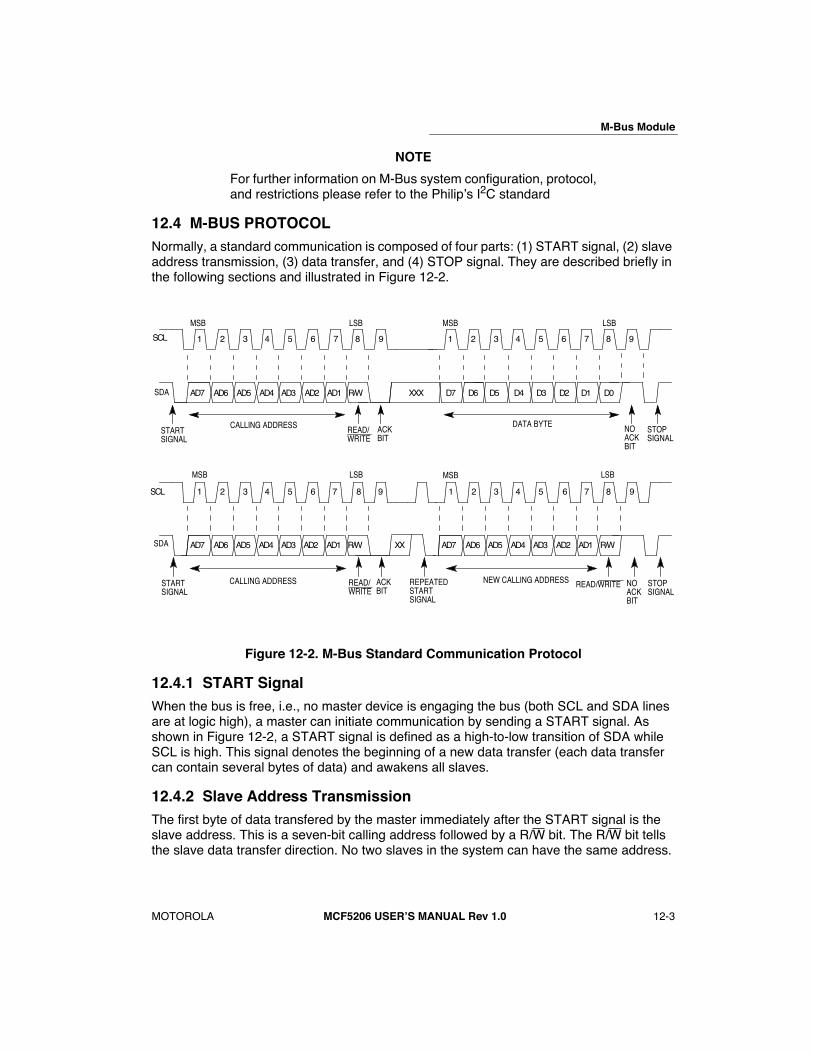
M-Bus Module
MOTOROLA
MCF5206 USERÕS MANUAL Rev 1.0
12-3
2
3
4
6
7
8
9
10
11
12
13
14
16
1
NOTE
For further information on M-Bus system configuration, protocol,and restrictions please refer to the PhilipÕs I
2
C standard
12.4 M-BUS PROTOCOL
Normally, a standard communication is composed of four parts: (1) START signal, (2) slave address transmission, (3) data transfer, and (4) STOP signal. They are described briefly in the following sections and illustrated in Figure 12-2.
12.4.1 START Signal
When the bus is free, i.e., no master device is engaging the bus (both SCL and SDA lines are at logic high), a master can initiate communication by sending a START signal. As shown in Figure 12-2, a START signal is defined as a high-to-low transition of SDA while SCL is high. This signal denotes the beginning of a new data transfer (each data transfer can contain several bytes of data) and awakens all slaves.
12.4.2 Slave Address Transmission
The first byte of data transfered by the master immediately after the START signal is the slave address. This is a seven-bit calling address followed by a R/W bit. The R/W bit tells the slave data transfer direction. No two slaves in the system can have the same address.
Figure 12-2. M-Bus Standard Communication Protocol
1 2 3 4 5 6 7 8 1 2 3 4 5 6 7 8
SCL 1 2 3 4 5 6 7 8 1 2 5 6 7 83 4
9 9
AD7 AD6 AD5 AD4 AD3 AD2 AD1 R/W XXX D7 D6 D5 D4 D3 D2 D1 D0
AD7 AD6 AD5 AD4 AD3 AD2 AD1 R/W AD7 AD6 AD5 AD4 AD3 AD2 AD1 R/W
9 9
XX
NEW CALLING ADDRESS READ/WRITE NO ACK BIT
STOPSIGNAL
REPEATEDSTARTSIGNAL
ACKBIT
READ/WRITE
CALLING ADDRESSSTARTSIGNAL
SDA
MSB LSB
STARTSIGNAL
CALLING ADDRESS READ/WRITE
ACKBIT
MSB LSB
DATA BYTE NO ACK BIT
STOPSIGNAL
LSBMSBLSBMSB
SDA
SCL
M-Bus Module
12-4
MCF5206 USERÕS MANUAL Rev 1.0
MOTOROLA
2
4
5
6
7
8
9
10
11
12
13
14
15
16
1
In addition, if the M-Bus is master, it must not transmit an address that is equal to its slave address. The M-Bus cannot be master and slave at the same time.
Only the slave with a calling address that matches the one transmitted by the master responds by returning an acknowledge bit by pulling the SDA low at the 9th clock (see Figure 12-2).
12.4.3 Data Transfer
Once successful slave addressing is achieved, the data transfer can proceed on a byte-by-byte basis in the direction specified by the R/W bit sent by the calling master.
Each data byte is 8 bits long. Data can be changed only while SCL is low and must be held stable while SCL is high, as shown in Figure 12-2. There is one clock pulse on SCL for each data bit with the MSB being transferred first. Each byte data must be followed by an acknowledge bit, which is signalled from the receiving device by pulling the SDA low at the ninth clock. One complete data byte transfer needs nine clock pulses.
If the slave receiver does not acknowledge the master, the SDA line must be left high by the slave. The master can then generate a stop signal to abort the data transfer or a start signal (repeated start) to commence a new calling.
If the master receiver does not acknowledge the slave transmitter after a byte transmission, it means 'Ôend of data'Õ to the slave. The slave releases the SDA line for the master to generate STOP or START signal.
12.4.4 Repeated START Signal
As shown in Figure 12-2, a repeated START signal is a START signal generated without first generating a STOP signal to terminate the communication. The master uses this method to communicate with another slave or with the same slave in different mode (transmit/receive mode) without releasing the bus.
12.4.5 STOP Signal
The master can terminate the communication by generating a STOP signal to free the bus. However, the master can generate a START signal followed by a calling command without generating a STOP signal first. This is called repeated START. A STOP signal is defined as a low-to-high transition of SDA while SCL at logical Ò1Ó (see Figure 12-2). Note that a master can generate a STOP even if the slave has done an acknowledgement at which point the slave must release the bus.
12.4.6 Arbitration Procedure
M-Bus is a true multimaster bus that allows more than one master to be connected on it. If two or more masters try to simultaneously control the bus, a clock synchronization procedure determines the bus clock, for which the low period is equal to the longest clock low period and the high is equal to the shortest one among the masters. A data arbitration procedure determines the relative priority of the contending masters. A bus master loses arbitration if it transmits logic Ò1Ó while another master transmits logic Ò0.Ó The losing masters

M-Bus Module
MOTOROLA
MCF5206 USERÕS MANUAL Rev 1.0
12-5
2
3
4
6
7
8
9
10
11
12
13
14
16
1
immediately switch over to slave-receive mode and stop driving SDA output. In this case, the transition from master to slave mode does not generate a STOP condition. Meanwhile, hardware sets a status bit to indicate loss of arbitration.
12.4.7 Clock Synchronization
Because wire-AND logic is performed on SCL line, a high-to-low transition on SCL line affects all the devices connected on the bus. The devices start counting their low period when the master drives the SCL line low. Once a device clock has gone low, it holds the SCL line low until the clock high state is reached. However, the change of low to high in this device clock may not change the state of the SCL line if another device clock is still within its low period. Therefore, synchronized clock SCL is held low by the device with the longest low period. Devices with shorter low periods enter a high wait state during this time (see Figure 12-3). When all devices concerned have counted off their low period, the synchronized clock SCL line is released and pulled high. There is then no difference between the device clocks and the state of the SCL line and all the devices start counting their high periods. The first device to complete its high period pulls the SCL line low again.
12.4.8 Handshaking
The clock synchronization mechanism can be used as a handshake in data transfer. Slave devices can hold the SCL low after completion of one byte transfer (9 bits). In such cases, it halts the bus clock and forces the master clock into wait states until the slave releases the SCL line.
12.4.9 Clock Stretching
Slaves can use the clock synchronization mechanism to slow down the transfer bit rate. After the master has driven SCL low the slave can drive SCL low for the required period and
Figure 12-3. Synchronized Clock SCL
INTERNAL COUNTER RESET
SCL1
SCL2
SCL
WAIT START COUNTING HIGH PERIOD
M-Bus Module
12-6
MCF5206 USERÕS MANUAL Rev 1.0
MOTOROLA
2
4
5
6
7
8
9
10
11
12
13
14
15
16
1
then release it. If the slave SCL low period is greater than the master SCL low period,the resulting SCL bus signal low period is stretched.
12.5 PROGRAMMING MODEL
Five registers are used in the M-Bus interface and the internal configuration of these registers is discussed in the following paragraphs.The programmerÕs model of the M-Bus interface is shown below in Table 12-1.
A block diagram of the M-Bus system is shown in Figure 12-1.
12.5.1 M-Bus Address Register (MADR)
This register contains the address the M-Bus responds to when addressed as a slave; note that it is not the address sent on the bus during the address transfer.
ADR7ÐADR1 Ñ Slave AddressBits1 to 7 contain the specific slave address to be used by the M-Bus module.
NOTE
The default mode of M-Bus is slave mode for an address matchon the bus.
12.5.2 M-Bus Frequency Divider Register (MFDR)
MBC5ÐMBC0 Ñ M-Bus Clock Rate 5Ð0 This field is used to prescale the clock for bit rate selection. Due to the potential slow riseand fall times of the SCL and SDA signals, the bus signals are sampled at the prescaler
Table 12-1. M-Bus Interface ProgrammerÕs Model
ADDRESS M-BUS MODULE REGISTERS
MBAR+$1E0 M-Bus Address register (MADR)
MBAR+$1E4 M-Bus Frequency Divider Register (MFDR)
MBAR+$1E8 M-Bus Control Register (MBCR)
MBAR+$1EC M-Bus Status Register (MBSR)
MBAR+$1F0 M-Bus Data I/O Register (MBDR)
M-Bus Address Register (MADR)
Address MBAR+$1E0
7 6 5 4 3 2 1 0
ADR7 ADR6 ADR5 ADR4 ADR3 ADR2 ADR1 -
RESET 0 0 0 0 0 0 0 0
Read/Write
Supervisor or User Mode
M-Bus Frequency Divider Register (MFDR)
Address MBAR+$1E4
7 6 5 4 3 2 1 0
- - MBC5 MBC4 MBC3 MBC2 MBC1 MBC0
RESET 0 0 0 0 0 0 0 0
Read/Write
Supervisor or User Mode
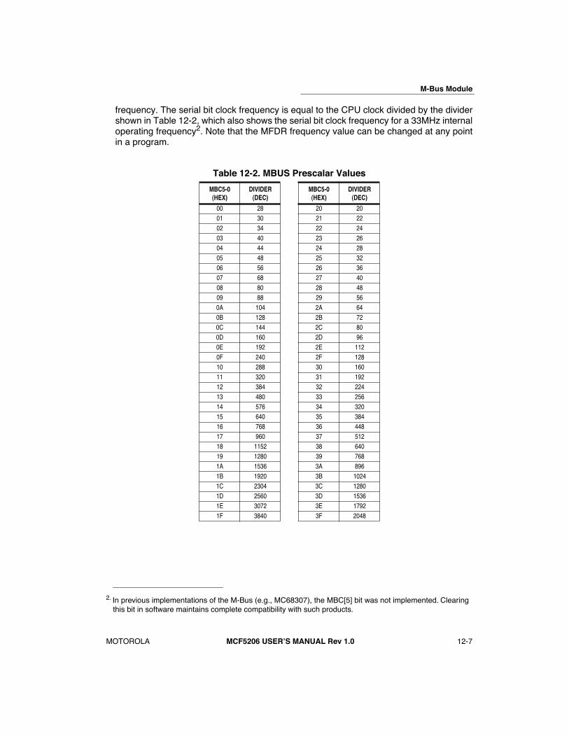
M-Bus Module
MOTOROLA
MCF5206 USERÕS MANUAL Rev 1.0
12-7
2
3
4
6
7
8
9
10
11
12
13
14
16
1
frequency. The serial bit clock frequency is equal to the CPU clock divided by the dividershown in Table 12-2, which also shows the serial bit clock frequency for a 33MHz internaloperating frequency
2
. Note that the MFDR frequency value can be changed at any pointin a program.
2.
In previous implementations of the M-Bus (e.g., MC68307), the MBC[5] bit was not implemented. Clearing this bit in software maintains complete compatibility with such products.
Table 12-2. MBUS Prescalar Values
MBC5-0(HEX)
DIVIDER(DEC)
MBC5-0(HEX)
DIVIDER(DEC)
00 28 20 2001 30 21 2202 34 22 2403 40 23 2604 44 24 2805 48 25 3206 56 26 3607 68 27 4008 80 28 4809 88 29 560A 104 2A 640B 128 2B 720C 144 2C 800D 160 2D 960E 192 2E 1120F 240 2F 12810 288 30 16011 320 31 19212 384 32 22413 480 33 25614 576 34 32015 640 35 38416 768 36 44817 960 37 51218 1152 38 64019 1280 39 7681A 1536 3A 8961B 1920 3B 10241C 2304 3C 12801D 2560 3D 15361E 3072 3E 17921F 3840 3F 2048
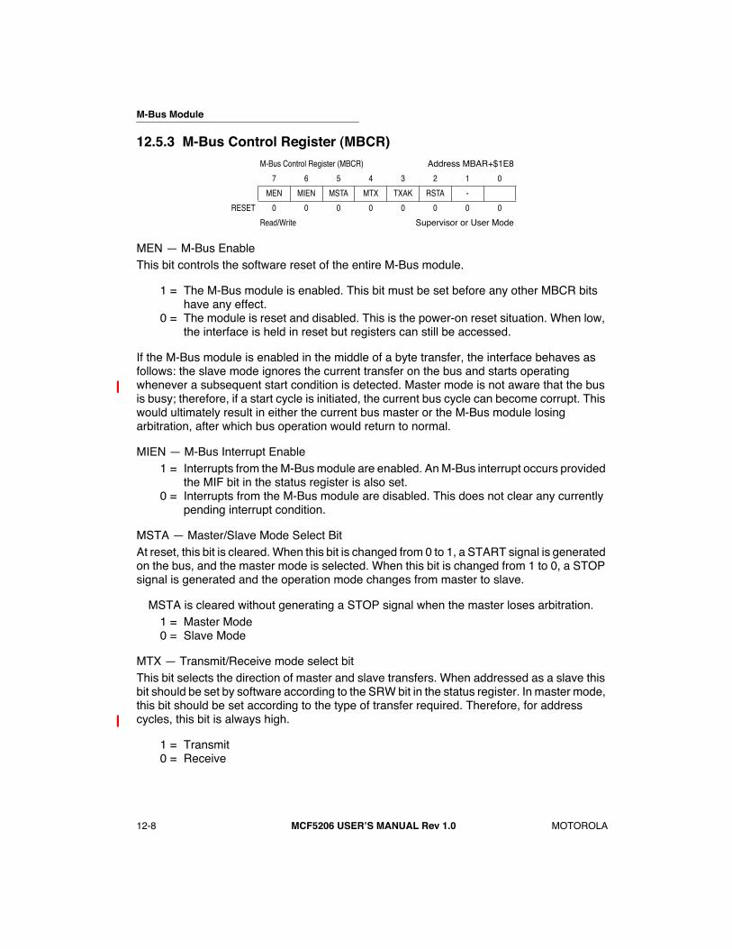
M-Bus Module
12-8
MCF5206 USERÕS MANUAL Rev 1.0
MOTOROLA
2
4
5
6
7
8
9
10
11
12
13
14
15
16
1
12.5.3 M-Bus Control Register (MBCR)
MEN Ñ M-Bus EnableThis bit controls the software reset of the entire M-Bus module.
1 = The M-Bus module is enabled. This bit must be set before any other MBCR bits have any effect.
0 = The module is reset and disabled. This is the power-on reset situation. When low, the interface is held in reset but registers can still be accessed.
If the M-Bus module is enabled in the middle of a byte transfer, the interface behaves as follows: the slave mode ignores the current transfer on the bus and starts operating whenever a subsequent start condition is detected. Master mode is not aware that the bus is busy; therefore, if a start cycle is initiated, the current bus cycle can become corrupt. This would ultimately result in either the current bus master or the M-Bus module losing arbitration, after which bus operation would return to normal.
MIEN Ñ M-Bus Interrupt Enable 1 = Interrupts from the M-Bus module are enabled. An M-Bus interrupt occurs provided
the MIF bit in the status register is also set.0 = Interrupts from the M-Bus module are disabled. This does not clear any currently
pending interrupt condition.
MSTA Ñ Master/Slave Mode Select Bit At reset, this bit is cleared. When this bit is changed from 0 to 1, a START signal is generated on the bus, and the master mode is selected. When this bit is changed from 1 to 0, a STOP signal is generated and the operation mode changes from master to slave.
MSTA is cleared without generating a STOP signal when the master loses arbitration.1 = Master Mode0 = Slave Mode
MTX Ñ Transmit/Receive mode select bit This bit selects the direction of master and slave transfers. When addressed as a slave this bit should be set by software according to the SRW bit in the status register. In master mode, this bit should be set according to the type of transfer required. Therefore, for address cycles, this bit is always high.
1 = Transmit0 = Receive
M-Bus Control Register (MBCR)
Address MBAR+$1E8
7 6 5 4 3 2 1 0
MEN MIEN MSTA MTX TXAK RSTA -
RESET 0 0 0 0 0 0 0 0
Read/Write
Supervisor or User Mode

M-Bus Module
MOTOROLA
MCF5206 USERÕS MANUAL Rev 1.0
12-9
2
3
4
6
7
8
9
10
11
12
13
14
16
1
TXAK Ñ Transmit Acknowledge Enable This bit specifies the value driven onto SDA during acknowledge cycles for both master and slave receivers.
Note that writing this bit only applies when the M-Bus is a receiver, not a transmitter.
1 = No acknowledge signal response is sent (i.e., acknowledge bit = 1)0 = An acknowledge signal is sent out to the bus at the 9th clock bit after receiving one
byte data
RSTA Ñ Repeat Start Writing a 1 to this bit generates a repeated START condition on the bus, provided it is the current bus master. This bit is always read as a low. Attempting a repeated start at the wrong time, if the bus is owned by another master, results in loss of arbitration. Note that this bit is not readable.
1 = Generate repeat start cycle
12.5.4 M-Bus Status Register (MBSR)
This status register is read-only with the exception of bit 1 (MIF) and bit 4 (MAL), which can be cleared by software. All bits are cleared on reset except bit 7 (MCF) and bit 0 (RXAK), which are set (=1) at reset.
MCF Ñ Data Transferring Bit While one byte of data is being transferred, this bit is cleared. It is set by the falling edge of the 9th clock of a byte transfer.
1 = Transfer complete0 = Transfer in progress
MAAS Ñ Addressed as a Slave Bit When its own specific address (M-Bus Address Register) is matched with the calling address, this bit is set. The CPU is interrupted provided the MIEN is set. Next, the CPU must check the SRW bit and set its TX/RX mode accordingly.
Writing to the M-Bus Control Register clears this bit. 1 = Addressed as a slave0 = Not addressed
M-Bus Status Register (MBSR)
Address MBAR+$1EC
7 6 5 4 3 2 1 0
MCF MAAS MBB MAL - SRW MIF RXAK
RESET 1 0 0 0 0 0 0 1
Read/Write
Supervisor or User Mode

M-Bus Module
12-10
MCF5206 USERÕS MANUAL Rev 1.0
MOTOROLA
2
4
5
6
7
8
9
10
11
12
13
14
15
16
1
MBB Ñ Bus Busy Bit This bit indicates the status of the bus. When a START signal is detected, the MBB is set. If a STOP signal is detected, it is cleared.
1 = Bus is busy0 = Bus is idle
MAL Ñ Arbitration Lost Hardware sets the arbitration lost bit (MAL) when the arbitration procedure is lost. Arbitration is lost in the following circumstances:
1. SDA sampled as low when the master drives a high during an address or data-transmit cycle.
2. SDA sampled as a low when the master drives a high during the acknowledge bit of a data-receive cycle.
3. A start cycle is attempted when the bus is busy.
4. A repeated start cycle is requested in slave mode.
5. A stop condition is detected when the master did not request it.
This bit must be cleared by software by writing a low to it.
SRW Ñ Slave Read/WriteWhen MAAS is set, this bit indicates the value of the R/W command bit of the calling address sent from the master. This bit is valid only when 1) a complete transfer has occurred and no other transfers have been initiated and 2) M-Bus is a slave and has an address match. Checking this bit, the CPU can select slave transmit/receive mode according to the command of the master.
1 = Slave transmit, master reading from slave0 = Slave receive, master writing to slave
MIF Ñ M-Bus InterruptThe MIF bit is set when an interrupt is pending, which causes a processor interrupt request (provided MIEN is set). MIF is set when one of the following events occurs:
1. Complete one byte transfer (set at the falling edge of the 9th clock)
2. Receive a calling address that matches its own specific address in slave-receive mode
3. Arbitration lost
This bit must be cleared by software by writing a low to it in the interrupt routine.
RXAK Ñ Received AcknowledgeThe value of SDA during the acknowledge bit of a bus cycle. If the received acknowledge bit (RXAK) is low, it indicates an acknowledge signal has been received after the completion
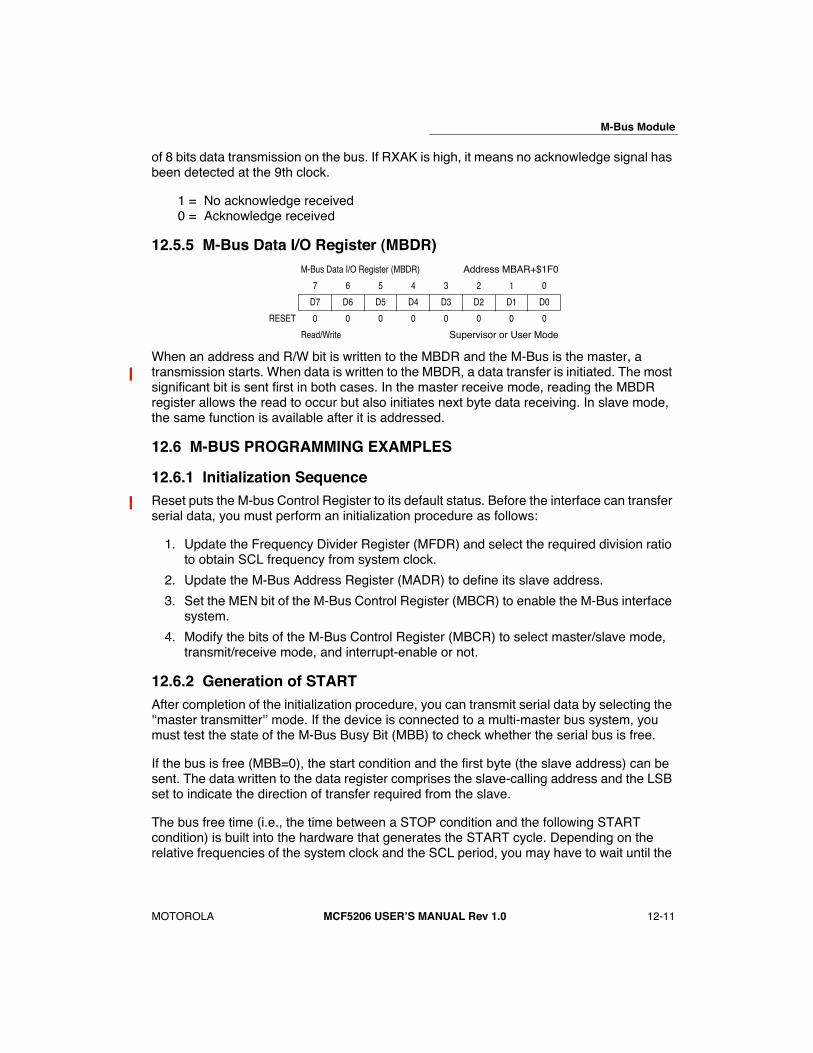
M-Bus Module
MOTOROLA
MCF5206 USERÕS MANUAL Rev 1.0
12-11
2
3
4
6
7
8
9
10
11
12
13
14
16
1
of 8 bits data transmission on the bus. If RXAK is high, it means no acknowledge signal has been detected at the 9th clock.
1 = No acknowledge received0 = Acknowledge received
12.5.5 M-Bus Data I/O Register (MBDR)
When an address and R/W bit is written to the MBDR and the M-Bus is the master, a transmission starts. When data is written to the MBDR, a data transfer is initiated. The most significant bit is sent first in both cases. In the master receive mode, reading the MBDR register allows the read to occur but also initiates next byte data receiving. In slave mode, the same function is available after it is addressed.
12.6 M-BUS PROGRAMMING EXAMPLES
12.6.1 Initialization Sequence
Reset puts the M-bus Control Register to its default status. Before the interface can transfer serial data, you must perform an initialization procedure as follows:
1. Update the Frequency Divider Register (MFDR) and select the required division ratio to obtain SCL frequency from system clock.
2. Update the M-Bus Address Register (MADR) to define its slave address.
3. Set the MEN bit of the M-Bus Control Register (MBCR) to enable the M-Bus interface system.
4. Modify the bits of the M-Bus Control Register (MBCR) to select master/slave mode, transmit/receive mode, and interrupt-enable or not.
12.6.2 Generation of START
After completion of the initialization procedure, you can transmit serial data by selecting the 'Ômaster transmitter'Õ mode. If the device is connected to a multi-master bus system, you must test the state of the M-Bus Busy Bit (MBB) to check whether the serial bus is free.
If the bus is free (MBB=0), the start condition and the first byte (the slave address) can be sent. The data written to the data register comprises the slave-calling address and the LSB set to indicate the direction of transfer required from the slave.
The bus free time (i.e., the time between a STOP condition and the following START condition) is built into the hardware that generates the START cycle. Depending on the relative frequencies of the system clock and the SCL period, you may have to wait until the
M-Bus Data I/O Register (MBDR)
Address MBAR+$1F0
7 6 5 4 3 2 1 0
D7 D6 D5 D4 D3 D2 D1 D0
RESET 0 0 0 0 0 0 0 0
Read/Write
Supervisor or User Mode
M-Bus Module
12-12
MCF5206 USERÕS MANUAL Rev 1.0
MOTOROLA
2
4
5
6
7
8
9
10
11
12
13
14
15
16
1
M-Bus is busy after writing the calling address to the MBDR before proceeding with the following instructions.
An example of a program that generates the START signal and transmits the first byte of data (slave address) is shown below:
CHFLAGMOVE.BMBSR,-(A7); CHECK THE MBB BIT OF THE STATUS REGISTER. IF IT ISBTST.B#5, (A7)+ SET, WAIT UNTIL IT IS CLEARBNE.SCHFLAG;
TXSTARTMOVE.BMBCR,-(A7); SET TRANSMIT MODEBSET.B#4,(A7)
MOVE.B(A7)+, MBCRMOVE.BMBCR, -(A7); SET MASTER MODEBSET.B#5, (A7); i.e. GENERATE START CONDITION MOVE.B(A7)+, MBCR;MOVE.BCALLING,-(A7); TRANSMIT THE CALLING ADDRESS, D0=R/WMOVE.B(A7)+, MBDR; MBFREEMOVE.BMBSR,-(A7); CHECK THE MBB BIT OF THE STATUS REGISTER. IF IT ISBTST.B#5, (A7)+; CLEAR, WAIT UNTIL IT IS SETBEQ.SMBFREE;
12.6.3 Post-Transfer Software Response
Transmission or reception of a byte sets the data transferring bit (MCF) to 1, which indicates one byte communication is finished. The M-Bus interrupt bit (MIF) is also set ; an interrupt is generated if the interrupt function is enabled during initialization by setting the MIEN bit. Software must clear the MIF bit in the interrupt routine first. The MCF bit is cleared by reading from the M-Bus Data I/O Register (MDR) in receive mode or writing to MDR in transmit mode.
Software can service the M-bus I/O in the main program by monitoring the MIF bit if the interrupt function is disabled. Polling should monitor the MIF bit rather than the MCF bit because that operation is different when arbitration is lost.
When an interrupt occurs at the end of the address cycle, the master is always in transmit mode, i.e. the address is transmitted. If master receive mode is required, indicated by R/W bit in MBDR, then the MTX bit should be toggled at this stage.
During slave-mode address cycles (MAAS=1), the SRW bit in the status register is read to determine the direction of the subsequent transfer and the MTX bit is programmed accordingly. For slave-mode data cycles (MAAS=0), the SRW bit is not valid. The MTX bit in the control register should be read to determine the direction of the current transfer.
The following is an example of a software response by a 'Ômaster transmitterÕ' in the interrupt routine (see Figure 12-4).

M-Bus Module
MOTOROLA
MCF5206 USERÕS MANUAL Rev 1.0
12-13
2
3
4
6
7
8
9
10
11
12
13
14
16
1
ISRLEA.LMBSR,-(A7); LOAD EFFECTIVE ADDRESSBCLR.B#1,(A7)+; CLEAR THE MIF FLAGMOVE.BMBCR,-(A7); PUSH ADDRESS ON STACK,BTST.B#5,(A7)+; CHECK THE MSTA FLAGBEQ.SSLAVE; BRANCH IF SLAVE MODEMOVE.BMBCR,-(A7); PUSH ADDRESS ON STACKBTST.B#4,(A7)+; CHECK THE MODE FLAGBEQ.SRECEIVE; BRANCH IF IN RECEIVE MODEMOVE.BMBSR,-(A7); PUSH ADDRESS ON STACK,BTST.B#0,(A7)+; CHECK ACK FROM RECEIVERBNE.B END; IF NO ACK, END OF TRANSMISSIONTRANSMITMOVE.BDATABUF,-(A7); STACK DATA BYTEMOVE.B(A7)+, MBDR; TRANSMIT NEXT BYTE OF DATA
12.6.4 Generation of STOP
A data transfer ends with a STOP signal generated by the 'ÔmasterÕ' device. A master transmitter can generate a STOP signal after all the data has been transmitted. The following is an example showing how a master transmitter generates a stop condition.
MASTXMOVE.BMBSR, -(A7); IF NO ACK, BRANCH TO ENDBTST.B#0,(A7)+BNE.B ENDMOVE.BTXCNT,D0; GET VALUE FROM THE TRANSMITTING COUNTERBEQ.SEND; IF NO MORE DATA, BRANCH TO ENDMOVE.BDATABUF,-(A7); TRANSMIT NEXT BYTE OF DATAMOVE.B(A7)+,MBDRMOVE.BTXCNT,D0; DECREASE THE TXCNTSUBQ.L#1,D0MOVE.BD0,TXCNTBRA.SEMASTX; EXIT ENDLEA.LMBCR,-(A7); GENERATE A STOP CONDITIONBCLR.B#5,(A7)+EMASTXRTE; RETURN FROM INTERRUPT
If a master receiver wants to terminate a data transfer, it must inform the slave transmitter by not acknowledging the last byte of data, which can be done by setting the transmit acknowledge bit (TXAK) before reading the 2nd last byte of data. Before reading the last byte of data, a STOP signal must be generated first. The following is an example showing how a master receiver generates a STOP signal.
MASRMOVE.BRXCNT,D0; DECREASE RXCNTSUBQ.L#1,D0MOVE.BD0,RXCNTBEQ.SENMASR; LAST BYTE TO BE READMOVE.BRXCNT,D1; CHECK SECOND LAST BYTE TO BE READ (NOT LAST ONE OR SECOND LASTEXTB>LD1SUBI.L#1,D1; BNE.SNXMARLAMARBSET.B#3,MBCR; SECOND LAST, DISABLE ACK TRANSMITTINGBRANXMAR
M-Bus Module
12-14
MCF5206 USERÕS MANUAL Rev 1.0
MOTOROLA
2
4
5
6
7
8
9
10
11
12
13
14
15
16
1
ENMASRBCLR.B#5,MBCR; LAST ONE, GENERATE 'STOPÕ SIGNALNXMARMOVE.BMBDR,RXBUF; READ DATA AND STORE RTE
12.6.5 Generation of Repeated START
At the end of data transfer, if the master still wants to communicate on the bus, it can generate another START signal followed by another slave address without first generating a STOP signal. A program example is as shown.
RESTARTMOVE.BMBCR,-(A7); ANOTHER START (RESTART)BSET.B#2, (A7)MOVE.B(A7)+, MBCRMOVE.BCALLING,-(A7); TRANSMIT THE CALLING ADDRESS, D0=R/W-MOVE.BCALLING,-(A7); MOVE.B(A7)+, MBDR
12.6.6 Slave Mode
In the slave interrupt service routine, the module addressed as slave bit (MAAS) should be tested to check if a calling of its own address has just been received. If MAAS is set, software should set the transmit/receive mode select bit (MTX bit of MBCR) according to the R/W command bit (SRW). Writing to the MBCR clears the MAAS automatically. The only time MAAS is read as set is from the interrupt at the end of the address cycle where an address match occurred; interrupts resulting from subsequent data transfers have MAAS cleared. A data transfer can now be initiated by writing information to MBDR, for slave transmits, or dummy reading from MBDR, in slave-receive mode. The slave drives SCL low in between byte transfers. SCL is released when the MBDR is accessed in the required mode.
In slave transmitter routine, the received acknowledge bit (RXAK) must be tested before transmitting the next byte of data. Setting RXAK means an 'Ôend-of-dataÕ' signal from the master receiver, after which it must be switched from transmitter mode to receiver mode by software. A dummy read then releases the SCL line so that the master can generate a STOP signal.
12.6.7 Arbitration Lost
If several masters try to simultaneously engage the bus, only one master wins and the others lose arbitration. The devices that lost arbitration are immediately switched to slave receive mode by the hardware. Their data output to the SDA line is stopped, but SCL is still generated until the end of the byte during which arbitration was lost. An interrupt occurs at the falling edge of the ninth clock of this transfer with MAL=1 and MSTA=0. If one master tries to transmit or do a START while the bus is being engaged by another master, the hardware : (1) inhibits the transmission, (2) switches the MSTA bit from 1 to 0 without generating STOP condition, (3) generates an interrupt to CPU and, (4) sets the MAL to indicate the failed attempt to engage the bus. When considering these cases, the slave service routine should test the MAL first and the software should clear the MAL bit if it is set.

M-Bus Module
MOTOROLA
MCF5206 USERÕS MANUAL Rev 1.0
12-15
2
3
4
6
7
8
9
10
11
12
13
14
16
1
Figure 12-4. Flow-Chart of Typical M-Bus Interrupt Routine
CLEAR
MASTER MODE
?
TX/RX ?
LAST BYTE TRANSMITTED
?
RXAK=0 ?
END OF ADDR CYCLE (MASTER RX)
?
WRITE NEXTBYTE TO MBDR
SWITCH TO RX MODE
DUMMY READ FROM MBDR
GENERATE STOP SIGNAL
READ DATA FROM MBDR AND STORE
SET TXAK =1 GENERATE STOP SIGNAL
2ND LAST BYTE TO BE READ
?
LAST BYTE TO BE READ
?
ARBITRATION LOST
?
CLEAR MAL
MAAS=1 ?
MAAS=1 ?
SRW=1 ?
TX/RX ?
SET TX MODE
WRITE DATA TO MBDR
SET RX MODE
DUMMY READ FROM MBDR
ACK FROMRECEIVER
?
TX NEXT BYTE
READ DATA FROM MBDR AND STORE
SWITCH TO RX MODE
DUMMY READ FROM MBDR
RTE
Y N
Y
Y Y
Y
Y
Y
Y
Y
Y
N
N
N
NN
N
N
N
N
Y
TX RX
RX
TX(WRITE)
(READ)
N
MIF
ADDRESSCYCLE
DATACYCLE
MOTOROLA
MCF5206 USERÕS MANUAL Rev 1.0
13-1
2
3
4
5
6
7
8
9
10
11
12
13
14
15
16
1
SECTION 13TIMER MODULE
13.1 OVERVIEW OF THE TIMER MODULE
The MCF5206 contains two general-purpose16-bit timers. This section of the manual documents how the 16-bit timer operates.
The output of an 8-bit prescaler clocks each 16-bit timer. The prescaler input can be the system clock, the system clock divided by 16, or the timer input (TIN) pin. Figure 13-1 is a block diagram of the Timer module.
13.2 OVERVIEW OF KEY FEATURES
The general-purpose 16-bit timer unit has the following features:
¥ Maximum period of 8 seconds at 33 MHz, 11 seconds at 25 MHz, and 16 seconds at 16.67 MHz
¥ 30 ns resolution at 33 MHz, 40 ns at 25 MHz, 60 ns at 16.67 MHz
¥ Programmable sources for the clock input, including external clock
¥ Input-capture capability with programmable trigger edge on input pin
¥ Output-compare with programmable mode for the output pin
¥ Free run and restart modes
¥ Maskable interrupts on input capture or reference-compare
DATE: 9-2-98
REVISION NO.: 1.1
PAGES AFFECTED: SEE CHANGE BARS

Timer Module
13-2
MCF5206 USERÕS MANUAL Rev 1.0
MOTOROLA
2
3
4
5
6
7
8
9
10
11
12
13
14
15
16
1
Figure 13-1. Timer Block Diagram Module Operation
13.3 UNDERSTANDING THE GENERAL-PURPOSE TIMER UNITS
The general-purpose timer units provide the following features:
¥ You can program timers to count and compare to a reference value stored in a register or capture the timer value at an edge detected on the TIN pin
¥ An 8-bit prescalar output clocks the timers
¥ You can program the prescalar clock input
¥ Programmed events generate interrupts
¥ You can configure the TOUT pin to toggle or pulse on an event
The maximum resolution of each timer is one system clock cycle (30 ns at 33 MHz). To obtain the maximum period, divide the system clock by 16, set the prescaler value to divide by 256, and load the reference value with ones. This maximum period is 268,435,456 cycles (8.05 seconds at 33 MHz).
TIMER CLOCK
GENERATOR
DIVIDER
MODE REGISTERPRESCALER MODE BITS
TIMER COUNTER
15 0
CAPTURE REGISTER
15 0
REFERENCE REGISTER
15 0
15 0
7 0
EVENT REG
CAPTURE DETECTION
SYSTEM CLOCK OR SYSTEM CLOCK/16
TIN
TOUT D
ATA
BUS
(16)
GENERAL-PURPOSE TIMER
CLOCK
IRQ
BUS
Timer Module
MOTOROLA
MCF5206 USERÕS MANUAL Rev 1.0
13-3
2
3
4
5
6
7
8
9
10
11
12
13
14
15
16
1
13.3.1 Selecting the Prescaler
You can select the prescalar clock from the main clock (divided by 1 or by 16) or from the corresponding timer input TIN pin. TIN is synchronized to the internal clock. The synchronization delay is between two and three main clocks. TIN must meet the setup time spec shown in the AC Electrical Specs section.
The ICLK bits of the corresponding Timer Mode Register (TMR) select the clock input source. The prescaler is programmed to divide the clock input by values from 1 to 256. The prescalar output is used as an input to the 16-bit counter.
13.3.2 Working with Capture Mode
The timer has a 16-bit Timer Capture Register (TCR) that latches the counter value when the corresponding input capture-edge detector senses a defined transition (of TIN). The capture edge (CE) bits in the TMR select the type of transition triggering the capture. A capture event sets the Timer Event Register (TER) bit and issues a maskable interrupt.
13.3.3 Configuring the Timer for Reference Compare
You can configure the timer to count until it reaches a reference value at which time it either starts a new time count immediately or continues to run. The free run/restart (FRR) bit of the TMR selects either mode. When the timer reaches the reference value, the TER bit is set and issues an interrupt if the output reference interrupt (ORI) enable bit in TMR is set.
13.3.4 Configuring the Timer for Output Mode
The timer can send an output signal on the timer output (TOUT) pin when it reaches the reference value as selected by the output mode (OM) bit in the TMR. This signal can be an active-low pulse or a toggle of the current output under program control.
13.3.5 Interrupts
You can program the timer modules interrupt levels and priorities using the interrupt level (IL2 - IL0) and interrupt priority (IP1, IP0) bits in the appropriate interrupt control registers (ICR9, ICR10). The timer peripherals cannot provide interrupt vectors. Thus, autovector bits in ICR9 and ICR10 are set to 1. You cannot change this value. This generates autovectors in response to all timer interrupts.

Timer Module
13-4
MCF5206 USERÕS MANUAL Rev 1.0
MOTOROLA
2
3
4
5
6
7
8
9
10
11
12
13
14
15
16
1
13.4 PROGRAMMING MODEL
13.4.1 Understanding the General-Purpose Timer Registers
You can modify the timer registers at any time. Table 13-1 illustrates the programming model.
13.4.1.1 TIMER MODE REGISTER (TMR).
TMR is a 16-bit memory-mapped register. This register programs the various timer modes and is cleared by reset.
PS7ÐPS0 Ñ Prescaler ValueThe prescaler is programmed to divide the clock input by values from 1 to 256. The value 00000000 divides the clock by 1; the value 11111111 divides the clock by 256.
CE1ÐCE0 Ñ Capture Edge and Enable Interrupt11 = Capture on any edge and enable interrupt on capture event10 = Capture on falling edge only and enable interrupt on capture event 01 = Capture on rising edge only and enable interrupt on capture event 00 = Disable interrupt on capture event
OM Ñ Output Mode 1 = Toggle output0 = Active-low pulse for one system clock cycle (30ns at 33 MHz)
ORI Ñ Output Reference Interrupt Enable1 = Enable interrupt upon reaching the reference value0 = Disable interrupt for reference reached (does not affect interrupt on capture
function)
Table 13-1. Programming Model for Timers
TIMER 1ADDRESS
TIMER 2 ADDRESS SIM MODULEÐTIMER MODULE REGISTERS
MBAR+$100 MBAR+$120 Timer Mode Register (TMR)
MBAR+$104 MBAR+$124 Timer Reference Register (TRR)
MBAR+$108 MBAR+$128 Timer Capture Register (TCR)
MBAR+$10C MBAR+$12C Timer Counter (TCN)
MBAR+$111 MBAR+$131 Reserved Timer Event Register (TER)
Timer Mode Register (TMR) Address MBAR+$100, MBAR+$12015 14 13 12 11 10 9 8 7 6 5 4 3 2 1 0
PRESCALER VALUE (PS7 - PS0) CE1 - CE0 OM ORI FRR ICLK1 - ICLK0 RSTRESET 0 0 0 0 0 0 0 0 0 0 0 0 0 0 0 0
Read/Write Supervisor or User Mode
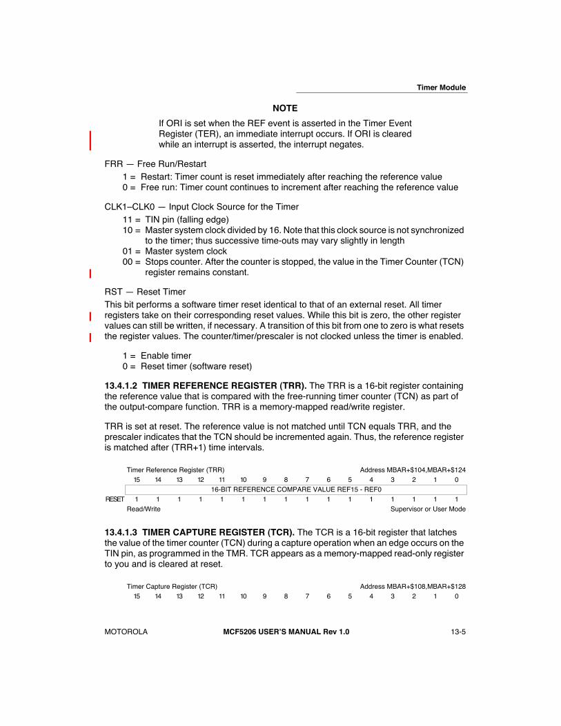
Timer Module
MOTOROLA
MCF5206 USERÕS MANUAL Rev 1.0
13-5
2
3
4
5
6
7
8
9
10
11
12
13
14
15
16
1
NOTE
If ORI is set when the REF event is asserted in the Timer EventRegister (TER), an immediate interrupt occurs. If ORI is clearedwhile an interrupt is asserted, the interrupt negates.
FRR Ñ Free Run/Restart1 = Restart: Timer count is reset immediately after reaching the reference value 0 = Free run: Timer count continues to increment after reaching the reference value
CLK1ÐCLK0 Ñ Input Clock Source for the Timer11 = TIN pin (falling edge)10 = Master system clock divided by 16. Note that this clock source is not synchronized
to the timer; thus successive time-outs may vary slightly in length01 = Master system clock 00 = Stops counter. After the counter is stopped, the value in the Timer Counter (TCN)
register remains constant.
RST Ñ Reset TimerThis bit performs a software timer reset identical to that of an external reset. All timer registers take on their corresponding reset values. While this bit is zero, the other register values can still be written, if necessary. A transition of this bit from one to zero is what resets the register values. The counter/timer/prescaler is not clocked unless the timer is enabled.
1 = Enable timer0 = Reset timer (software reset)
13.4.1.2 TIMER REFERENCE REGISTER (TRR).
The TRR is a 16-bit register containing the reference value that is compared with the free-running timer counter (TCN) as part of the output-compare function. TRR is a memory-mapped read/write register.
TRR is set at reset. The reference value is not matched until TCN equals TRR, and the prescaler indicates that the TCN should be incremented again. Thus, the reference register is matched after (TRR+1) time intervals.
13.4.1.3 TIMER CAPTURE REGISTER (TCR).
The TCR is a 16-bit register that latches the value of the timer counter (TCN) during a capture operation when an edge occurs on the TIN pin, as programmed in the TMR. TCR appears as a memory-mapped read-only register to you and is cleared at reset.
Timer Reference Register (TRR) Address MBAR+$104,MBAR+$12415 14 13 12 11 10 9 8 7 6 5 4 3 2 1 0
16-BIT REFERENCE COMPARE VALUE REF15 - REF0RESET 1 1 1 1 1 1 1 1 1 1 1 1 1 1 1 1
Read/Write Supervisor or User Mode
Timer Capture Register (TCR) Address MBAR+$108,MBAR+$12815 14 13 12 11 10 9 8 7 6 5 4 3 2 1 0

Timer Module
13-6
MCF5206 USERÕS MANUAL Rev 1.0
MOTOROLA
2
3
4
5
6
7
8
9
10
11
12
13
14
15
16
1
13.4.1.4 TIMER COUNTER (TCN).
TCN is a memory-mapped 16-bit up counter that you can read at any time. A read cycle to TCN yields the current timer value and does not affect the counting operation.
A write of any value to TCN causes it to reset to all zeros.
13.4.1.5 TIMER EVENT REGISTER (TER).
The TER is an 8-bit register that reports events the timer recognizes. When the timer recognizes an event, it sets the appropriate bit in the TER, regardless of the corresponding interrupt-enable bits (ORI and CE) in the TMR.
TER, which appears to you as a memory-mapped register, can be read at any time.
You should write a one to a bit to clear it (writing a zero does not affect bit value); more than one bit can be cleared at a time. The REF and CAP bits must be cleared before the timer negates the IRQ to the interrupt controller. Reset clears this register.
Bits 7Ð2 Ñ Reserved for future use.
CAP Ñ Capture Event If a one is read from this bit, the counter value has been latched into the TCR. The CE bit in the TMR enables the interrupt request caused by this event. You should write a one to this bit to clear the event condition.
REF Ñ Output Reference EventIf a one is read from this bit, the counter has reached the TRR value. The ORI bit in the TMR enables the interrupt request caused by this event. You should write a one to this bit to clear the event condition.
16-BIT CAPTURE COUNTER VALUE CAP15 - CAP0RESET 0 0 0 0 0 0 0 0 0 0 0 0 0 0 0 0
Read Only Supervisor or User Mode
Timer Counter Register (TCN) Address MBAR+$10C, MBAR+$12C15 14 13 12 11 10 9 8 7 6 5 4 3 2 1 0
16-BIT TIMER COUNTER VALUE COUNT15 - COUNT0RESET 0 0 0 0 0 0 0 0 0 0 0 0 0 0 0 0
Read/Write Supervisor or User Mode
Timer Event Register (TER) Address MBAR+$111,MBAR+$131
7 6 5 4
3 2 1 0
RESERVED REF CAP
RESET
0 0 0 0 0 0
0 0
Read/Write
Supervisor or User Mode

MOTOROLA
MCF5206 USERÕS MANUAL Rev 1.0
14-1
SECTION 14DEBUG SUPPORT
This section details the hardware debug support functions within the ColdFire 5200 Family of processors.
The general topic of debug support is divided into three separate areas:
1. Real-Time Trace Support
2. Background Debug Mode (BDM)
3. Real-Time Debug Support
Each area is addressed in detail in the following subsections.
The logic required to support these three areas is contained in a debug module, which is shown in the system block diagram in Figure 14-1.
14.1 REAL-TIME TRACE
In the area of debug functions, one fundamental requirement is support for real-time trace functionality (i.e., definition of the dynamic execution path). The ColdFire solution is to include a parallel output port providing encoded processor status and data to an external development system. This port is partitioned into two 4-bit nibbles: one nibble allows the processor to transmit information concerning the execution status of the core (processor status
,
PST[3:0]), while the other nibble allows data to be displayed (debug data
,
DDATA[3:0]).
Figure 14-1. Processor/Debug Module Interface
COLDFIRE CPU
DEBUG
MODULE
BDM PORT
DDATA, PSTDSCLK, DSI, DSO
INTERNAL BUSESCORE
TRACE PORT
DATE: 9-2-98
REVISION NO.: 1.1
PAGES AFFECTED: SEE CHANGE BARS
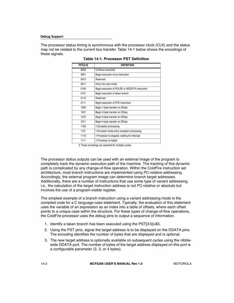
Debug Support
14-2
MCF5206 USERÕS MANUAL Rev 1.0
MOTOROLA
The processor status timing is synchronous with the processor clock (CLK) and the status may not be related to the current bus transfer. Table 14-1 below shows the encodings of these signals.
The processor status outputs can be used with an external image of the program to completely track the dynamic execution path of the machine. The tracking of this dynamic path is complicated by any change-of-flow operation. Within the ColdFire instruction set architecture, most branch instructions are implemented using PC-relative addressing. Accordingly, the external program image can determine branch target addresses. Additionally, there are a number of instructions that use some type of variant addressing, i.e., the calculation of the target instruction address is not PC-relative or absolute but involves the use of a program-visible register.
The simplest example of a branch instruction using a variant addressing mode is the compiled code for a C language
case
statement. Typically, the evaluation of this statement uses the variable of an expression as an index into a table of offsets, where each offset points to a unique case within the structure. For these types of change-of-flow operations, the ColdFire processor uses the debug pins to output a sequence of information.
1. Identify a taken branch has been executed using the PST[3:0]=$5.
2. Using the PST
pins, signal the target address is to be displayed on the DDATA pins. The encoding identifies the number of bytes that are displayed and is optional
.
3. The new target address is optionally available on subsequent cycles using the nibble-wide DDATA port. The number of bytes of the target address displayed on this port is a configurable parameter (2, 3, or 4 bytes).
Table 14-1. Processor PST Definition
PST[3:0] DEFINITION
0000 Continue execution
0001 Begin execution of an instruction
0010 Reserved
0011 Entry into user-mode
0100 Begin execution of PULSE or WDDATA instruction
0101 Begin execution of taken branch
0110 Reserved
0111 Begin execution of RTE instruction
1000 Begin 1-byte transfer on DData
1001 Begin 2-byte transfer on DData
1010 Begin 3-byte transfer on DData
1011 Begin 4-byte transfer on DData
1100 Exception processing
1101 Emulator-mode entry exception processing
1110 Processor is stopped, waiting for interrupt
1111 Processor is halted
These encodings are asserted for multiple cycles.

Debug Support
MOTOROLA
MCF5206 USERÕS MANUAL Rev 1.0
14-3
The nibble-wide DDATA port includes two 32-bit storage elements for capturing the CPU core bus information. These two elements effectively form a FIFO buffer connecting the core bus to the external development system. The FIFO buffer captures variant branch target addresses along with certain operand read/write data for eventual display on the DDATA
output port. The execution speed of the ColdFire processor is affected only when both storage elements contain valid data
waiting to be dumped onto the DDATA port. In this case, the processor core stalls until one FIFO entry is available. In all other cases, data output on the DDATA port does not impact execution speed.
From the processor core perspective, the PST outputs signal the
first AGEX cycle
of an instructionÕs execution. Most single-cycle instructions begin and complete their execution within a given machine cycle.
Because the processor status (PST[3:0]) values of $C, $D, $E, and $F define a multicycle mode or a special operation, the
PST outputs are driven with these values until the mode is exited or the operation completed. All the remaining fields specify information that is updated each machine cycle.
The status values of $8, $9, $A, and $B qualify the contents of the DDATA
output bus. These encodings are driven onto the PST port one machine cycle before the actual data is displayed on DDATA.
Figure14-3 shows the execution of an indirect JMP
instruction with the lower 16 bits of the target address being displayed on the DDATA output. In this diagram, the indirect JMP branches to address Òtarget.Ó The processor internally forms the PST marker ($9) one cycle before the address begins to appear on the DDATA
port. The target address is displayed on DDATA for four consecutive clocks, starting with the least-significant nibble. The processor continues execution, unaffected by the DDATA
bus activity.
Figure 14-2. Pipeline Timing Example (Debug Output)
The ColdFire instruction set architecture (ISA) includes a PULSE opcode. This opcode generates a unique PST encoding when executed (PST = $4). This instruction can define logic analyzer triggers for debug and/or performance analysis.
Last
DSOC AGEX
JMP (A0)
DSOC AGEX
Target
IAG IC DSOC AGEX
Target + $4
IAG IC DSOC AGEX
Internal PST
$5 $9 $0 TARGET
Internal DDATA
$0 $0 3:0 7:4 11:8 15:12
PST Pins
$5 $9 $0 TARGET
DDATA Pins
$0 $0 3:0 7:4 11:8 15:12

Debug Support
14-4
MCF5206 USERÕS MANUAL Rev 1.0
MOTOROLA
Additionally, a WDDATA opcode is supported that lets the processor core write any operand (byte, word, longword) directly to the DDATA port, independent of any Debug module configuration. This opcode also generates the special PST = $4 encoding when executed.
14.2 BACKGROUND-DEBUG MODE (BDM)
ColdFire 52xx processors support a modified version of the Background-Debug mode (BDM) functionality found on MotorolaÕs CPU32 Family of parts. BDM implements a low-level system debugger in the microprocessor hardware. Communication with the development system is handled via a dedicated, high-speed serial command interface (BDM port).
Unless noted otherwise, the BDM functionality provided by ColdFire 52xx processors is a proper subset of the CPU32 functionality. The main differences include the following:
¥ ColdFire implements the BDM controller in a dedicated hardware module. Although some BDM operations do require the CPU to be halted (e.g., CPU register accesses), other BDM commands such as memory accesses can be executed while the processor is running.
¥ DSCLK, DSI,
and DSO
are treated as synchronous signals, where the inputs (DSCLK and DSI) must meet the required input setup and hold timings, and the output (DSO) is specified as a delay relative to the rising edge of the processor clock.
¥ On CPU32 parts, DSO could signal hardware that a serial transfer can start. ColdFire clocking schemes restrict the use of this bit. Because DSO changes only when DSCLK is high, DSO cannot be used to indicate the start of a serial transfer. The development system should use either a free-running DSCLK or count the number of clocks in any given transfer.
¥ The Read/Write System Register commands (RSREG/WSREG) have been replaced by Read/Write Control Register commands (RCREG/WCREG). These commands use the register coding scheme from the MOVEC instruction.
¥ Read/Write Debug Module Register commands (RDMREG/WDMREG) have been add-ed to support Debug module register accesses.
¥ CALL and RST commands are not supported.
¥ Illegal command responses can be returned using the FILL and DUMP commands.
¥ For any command performing a byte-sized memory read operation, the upper 8 bits of the response data are undefined. The referenced data is returned in the lower 8 bits of the response.
¥ The debug module forces alignment for memory-referencing operations: long accesses are forced to a 0-modulo-4 address; word accesses are forced to a 0-modulo-2 address. An address error response can no longer be returned.
14.2.1 CPU Halt
Although some BDM operations can occur in parallel with CPU operation, unrestricted BDM operation requires the CPU to be halted. A number of sources can cause the CPU to halt, including the following (as shown in order of priority):

Debug Support
MOTOROLA
MCF5206 USERÕS MANUAL Rev 1.0
14-5
1. The occurrence of the catastrophic fault-on-fault condition automatically halts the processor. The halt status is posted on the PST port ($F).
2. The occurrence of a hardware breakpoint (reference subsection
Section 14.3 Real-Time Debug Support
) can be configured to generate a pending halt condition in a manner similar to the assertion of the BKPT signal. In some cases, the occurrence of this type of breakpoint halts the processor in an imprecise manner. Once the hardware breakpoint is asserted, the processor halts at the next sample point. See
Section 14.3.2 Theory of Operation
for more detail.
3. The execution of the HALT
(also known as BGND on the 683xx devices) instruction immediately suspends execution and posts the halt status ($F) on the PST
outputs. By default, this is a supervisor instruction and attempted execution while in user mode generates a privilege-violation exception. A User Halt Enable (UHE) control bit is provided in the Configuration/Status Register (CSR) to allow execution of HALT in user mode.
4. The assertion of the BKPT
input pin is treated as an pseudo-interrupt, i.e., the halt condition is made pending until the processor core samples for halts/interrupts. The processor samples for these conditions once during the execution of each instruction. If there is a pending halt condition at the sample time, the processor suspends execution and enters the halted state. The halt status ($F) is reflected in the PST outputs.
The halt source is indicated in CSR[27:24]; for simultaneous halt conditions, the highest priority source is indicated.
There are two special cases to be considered that involve the assertion of the BKPT pin.
After RSTI is negated, the processor waits for 16 clock cycles before beginning reset exception processing. If the BKPT input pin is asserted within the first eight cycles after RSTI is negated, the processor enters the halt state, signaling that status on the PST outputs ($F). While in this state, all resources accessible via the Debug module can be referenced. Once the system initialization is complete, the processor response to a BDM GO command depends on the set of BDM commands performed while Òbreakpointed.Ó Specifically, if the processorÕs PC register was loaded, the GO command causes the processor to exit the halt state and pass control to the instruction address contained in the PC. In this case, the normal reset exception processing is bypassed. Conversely, if the PC register was not loaded, the GO BDM command causes the processor to exit the halt state and continue with reset exception processing.
ColdFire 52xx processors also handle a special case with the assertion of BKPT while the processor is stopped by execution of the STOP instruction. For this case when the BKPT is asserted, the processor exits the stopped mode and enters the halted state. Once halted, the standard BDM commands may be exercised. When the processor is restarted, it continues with the execution of the next sequential instruction, i.e., the instruction following the STOP opcode.
The debug module Configuration/Status Register (CSR) maintains status defining the condition that caused the CPU to halt.

Debug Support
14-6
MCF5206 USERÕS MANUAL Rev 1.0
MOTOROLA
14.2.2 BDM Serial Interface
Once the CPU is halted and the halt status reflected on the PST outputs (PST[3:0]=$F), the development system can send unrestricted commands to the Debug module. The Debug module implements a synchronous protocol using a three-pin interface: development serial clock (DSCLK), development serial input (DSI), and
development serial output
(DSO). The development system serves as the serial communication channel master and is responsible for generation of the clock (DSCLK). The operating range of the serial channel is DC to one-half of the processor frequency. The channel uses a full duplex mode, where data is transmitted and received simultaneously by both master and slave devices.
Both DSCLK and DSI are synchronous inputs and must meet input setup and hold times with respect to CLK. DSCLK essentially acts as a pseudo Òclock enableÓ and is sampled on the rising edge of CLK. If the setup time of DSCLK is met, then the internal logic transitions on the rising edge of CLK, and DSI is sampled on the same CLK rising edge. The DSO output is specified as a delay from the DSCLK-enabled CLK rising edge. All events in the Debug moduleÕs serial state machine are based on the rising edge of the microprocessor clock. Refer to the
Electrical Characteristics
section of this manual
.
Figure 14-3. BDM Signal Sampling
The basic packet of information is a 17-bit word (16 data bits plus a status/control bit), as shown here.
Status/ControlThe status/control bit indicates the status of CPU-generated messages (always single word with the data field encoded as listed in Table 14-2). Command and data transfers initiated
16 15 0
S/C DATA FIELD [15:0]
CLK
DSCLK
DSI
DSO

Debug Support
MOTOROLA
MCF5206 USERÕS MANUAL Rev 1.0
14-7
by the development system should clear bit 16. The current implementation ignores this bit; however, Motorola has reserved this bit for future enhancements.
Data FieldThe data field contains the message data to be communicated between the development system and the Debug module.
14.2.3 BDM Command Set
ColdFire 52xx processors support a subset of BDM instructions from the current 683xx parts as well as extensions to provide access to new hardware features.
14.2.3.1 BDM COMMAND SET SUMMARY.
The BDM command set is summarized in Table 14-3. Subsequent paragraphs contain detailed descriptions of each command.
Table 14-2. CPU-Generated Message Encoding
S/C BIT DATA MESSAGE TYPE
0 xxxx Valid data transfer0 $FFFF Command complete; status OK1 $0000 Not ready with response; come again1 $0001 TEA-terminated bus error cycle; data invalid1 $FFFF Illegal command
Table 14-3. BDM Command Summary
COMMAND MNEMONIC DESCRIPTION CPU IMPACT
1
Read A/D Register RAREG/RDREG Read the selected address or data register and return the resultvia the serial BDM interface Halted
Write A/D Register WAREG/WDREG The data operand is written to the specified address or data register via the serial BDM interface Halted
Read Memory Location READ Read the sized data at the memory location specified by thelongword address
CycleSteal
Write Memory Location WRITE Write the operand data to the memory location specified by the longword address
CycleSteal
Dump Memory Block DUMP
Used in conjunction with the READ command to dump largeblocks of memory. An initial READ is executed to set up thestarting address of the block and to retrieve the first result.Subsequent operands are retrieved with the DUMP command.
CycleSteal
Fill Memory Block FILL
Used in conjunction with the WRITE command to fill largeblocks of memory. An initial WRITE is executed to set up thestarting address of the block and to supply the first operand.Subsequent operands are written with the FILL command.
CycleSteal
Resume Execution GO The pipeline is flushed and refilled before resuming instructionexecution at the current PC Halted
No Operation NOP NOP performs no operation and may be used as a null command Parallel
Read Control Register RCREG Read the system control register HaltedWrite Control Register WCREG Write the operand data to the system control register Halted
Read Debug Module Register RDMREG Read the Debug module register ParallelWrite Debug
Module Register WDMREG Write the operand data to the Debug module register Halted
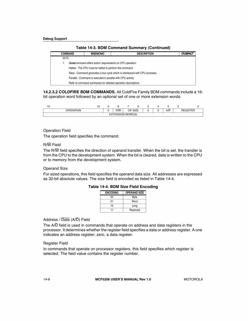
Debug Support
14-8
MCF5206 USERÕS MANUAL Rev 1.0
MOTOROLA
14.2.3.2 COLDFIRE BDM COMMANDS.
All ColdFire Family BDM commands include a 16-bit operation word followed by an optional set of one or more extension words.
Operation FieldThe operation field specifies the command.
R/W FieldThe R/W field specifies the direction of operand transfer. When the bit is set, the transfer is from the CPU to the development system. When the bit is cleared, data is written to the CPU or to memory from the development system.
Operand SizeFor sized operations, this field specifies the operand data size. All addresses are expressed as 32-bit absolute values. The size field is encoded as listed in Table 14-4.
Address / Data (A/D) FieldThe A/D field is used in commands that operate on address and data registers in the processor. It determines whether the register field specifies a data or address register. A one indicates an address register; zero, a data register.
Register FieldIn commands that operate on processor registers, this field specifies which register is selected. The field value contains the register number.
NOTE:
1.
General
command effect and/or requirements on CPU operation:
Halted - The CPU must be halted to perform this command
Steal - Command generates a bus cycle which is interleaved with CPU accesses
Parallel - Command is executed in parallel with CPU activity
Refer to command summaries for detailed operation descriptions.
15 10 9 8 7 6 5 4 3 2 0
OPERATION 0 R/W OP SIZE 0 0 A/D REGISTER
EXTENSION WORD(S)
Table 14-4. BDM Size Field Encoding
ENCODING OPERAND SIZE
00 Byte01 Word10 Long11 Reserved
Table 14-3. BDM Command Summary (Continued)
COMMAND MNEMONIC DESCRIPTION CPU IMPACT
1
Debug Support
MOTOROLA
MCF5206 USERÕS MANUAL Rev 1.0
14-9
Extension Word(s) (as required):Certain commands require extension words for addresses and/or immediate data. Addresses require two extension words because only absolute long addressing is permitted. Immediate data can be either one or two words in length; byte and word data each require a single extension word; longword data requires two words. Both operands and addresses are transferred by most significant word first. In the following descriptions of the BDM command set, the optional set of extension words are defined as the ÒOperand Data.Ó
14.2.3.3 Command Sequence Diagram.
A command sequence diagram (see Figure 14-4) illustrates the serial bus traffic for each command. Each bubble in the diagram represents a single 17-bit transfer across the bus. The top half in each diagram corresponds to the data transmitted by the development system to the debug module; the bottom half corresponds to the data returned by the debug module in response to the development system commands. Command and result transactions are overlapped to minimize latency.
The cycle in which the command is issued contains the development system command mnemonic (in this example, Òread memory locationÓ). During the same cycle, the debug module responds with either the lowest order results of the previous command or with a command complete status (if no results were required).
During the second cycle, the development system supplies the high-order 16 bits of the memory address. The debug module returns a Ònot readyÓ response($10000) unless the received command was decoded as unimplemented, in which case the response data is the illegal command ($1FFFF) encoding. If an illegal command response occurs, the development system should retransmit the command.
NOTE
The Ònot readyÓ response is ignored unless a memory bus cycleis in progress. Otherwise, the debug module can accept a newserial transfer after eight system clock periods.
In the third cycle, the development system supplies the low-order 16 bits of a memory address. The debug module always returns the Ònot readyÓ response in this cycle. At the completion of the third cycle, the debug module initiates a memory read operation. Any serial transfers that begin while the memory access is in progress return the Ònot readyÓ response.
Results are returned in the two serial transfer cycles following the completion of memory access. The data transmitted to the debug module during the final transfer is the opcode for the following command. Should a memory access generate a bus error, an error status ($10001) is returned in place of the result data.

Debug Support
14-10
MCF5206 USERÕS MANUAL Rev 1.0
MOTOROLA
Figure 14-4. Command Sequence Diagram
14.2.3.4 Command Set Descriptions.
The BDM command set is summarized in Table14-3.
Note
All the accompanying valid BDM results are defined with themost significant bit of the 17-bit response (S/C) as 0. Invalidcommand responses (Not Ready; TEA-terminated bus cycle; Il-legal Command) return a 1 in the most significant bit of the 17-bit response (S/C).
Motorola reserves unassigned command opcodes for future expansion. All unused com-mand formats within any revision level performs a NOP and return the ILLEGAL commandresponse.
COMMANDS TRANSMITTED TO THE DEBUG MODULE
COMMAND CODE TRANSMITTED DURING THIS CYCLE
HIGH-ORDER 16 BITS OF MEMORY ADDRESS
LOW-ORDER 16 BITS OF MEMORY ADDRESS
SEQUENCE TAKEN IFOPERATION HAS NOTCOMPLETED
DATA UNUSED FROMTHIS TRANSFER
SEQUENCE TAKEN IFILLEGAL COMMANDIS RECEIVED BY DEBUG MODULE
RESULTS FROM PREVIOUS COMMAND
RESPONSES FROM THE DEBUG MODULE
NONSERIAL-RELATED ACTIVITY
MS ADDR"NOT READY"
XXX"ILLEGAL"
LS ADDR"NOT READY"
NEXT CMD"NOT READY"
READ (LONG)???
NEXT CMD"NOT READY"
XXX"NOT READY"
XXXXX
XXXBERR
MS RESULTNEXT CMDLS RESULT
READMEMORYLOCATION
NEXTCOMMAND
CODE
SEQUENCE TAKEN IF BUS� ERROR OCCURS ONMEMORY ACCESS
HIGH- AND LOW-ORDER16 BITS OF RESULT
XXX

Debug Support
MOTOROLA
MCF5206 USERÕS MANUAL Rev 1.0
14-11
14.2.3.4.1 Read A/D Register (RAREG/RDREG).
Read the selected address or data register and return the 32-bit result. A bus error response is returned if the CPU core is not halted.
Formats:
Command Sequence:
Operand Data:None
Result Data:The contents of the selected register are returned as a longword value. The data is returnedmost significant word first.
15 14 13 12 11 10 9 8 7 6 5 4 3 2 1 0
$2 $1 $8 A/D REGISTER
RAREG/RDREG Command
15 14 13 12 11 10 9 8 7 6 5 4 3 2 1 0
DATA [31:16]
DATA [15:0]
RAREG/RDREG Result
XXXMS RESULT
NEXT CMDLS RESULT
RAREG/RDREG???
XXXBERR
NEXT CMD"NOT READY
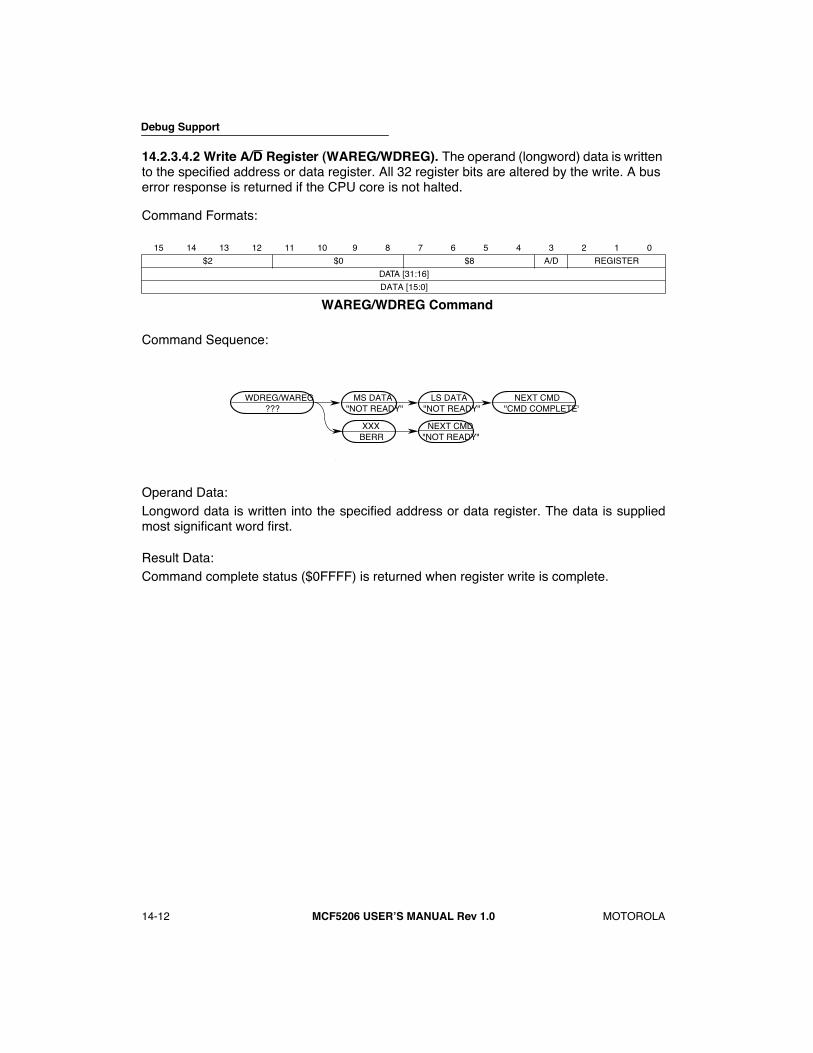
Debug Support
14-12
MCF5206 USERÕS MANUAL Rev 1.0
MOTOROLA
14.2.3.4.2 Write A/D Register (WAREG/WDREG).
The operand (longword) data is written to the specified address or data register. All 32 register bits are altered by the write. A bus error response is returned if the CPU core is not halted.
Command Formats:
Command Sequence:
Operand Data:Longword data is written into the specified address or data register. The data is suppliedmost significant word first.
Result Data:Command complete status ($0FFFF) is returned when register write is complete.
15 14 13 12 11 10 9 8 7 6 5 4 3 2 1 0
$2 $0 $8 A/D REGISTER
DATA [31:16]
DATA [15:0]
WAREG/WDREG Command
MS DATA"NOT READY"
XXX
LS DATA"NOT READY"
NEXT CMD"NOT READY"
WDREG/WAREG???
NEXT CMD"CMD COMPLETE"
BERR
Debug Support
MOTOROLA
MCF5206 USERÕS MANUAL Rev 1.0
14-13
14.2.3.4.3 Read Memory Location (READ).
Read the operand data from the memory location specified by the longword address. The address space is defined by the contents of the low-order 5 bits {TT, TM} of the address attribute register (AATR). The hardware forces the low-order bits of the address to zeros for word and longword accesses to ensure that operands are always accessed on natural boundaries: words on 0-modulo-2 addresses, longwords on 0-modulo-4 addresses.
Formats:
15 14 13 12 11 10 9 8 7 6 5 4 3 2 1 0
$1 $9 $0 $0
ADDRESS [31:16]
ADDRESS [15:0]
Byte READ Command
15 14 13 12 11 10 9 8 7 6 5 4 3 2 1 0
X X X X X X X X DATA [7:0]
Byte READ Result
15 14 13 12 11 10 9 8 7 6 5 4 3 2 1 0
$1 $9 $4 $0
ADDRESS [31:16]
ADDRESS [15:0]
Word READ Command
15 14 13 12 11 10 9 8 7 6 5 4 3 2 1 0
DATA [15:0]
Word READ Result
15 14 13 12 11 10 9 8 7 6 5 4 3 2 1 0
$1 $9 $8 $0
ADDRESS [31:16]
ADDRESS [15:0]
Long READ Command
15 14 13 12 11 10 9 8 7 6 5 4 3 2 1 0
DATA [31:16]
DATA [15:0]
Long READ Result
Debug Support
14-14
MCF5206 USERÕS MANUAL Rev 1.0
MOTOROLA
Command Sequence:
Operand Data:The single operand is the longword address of the requested memory location.
Result Data:The requested data is returned as either a word or longword. Byte data is returned in theleast significant byte of a word result, with the upper byte undefined. Word results return 16bits of significant data; longword results return 32 bits.
A successful read operation returns data bit 16 cleared. If a bus error is encountered, thereturned data is $10001.
MS ADDR"NOT READY"
LS ADDR"NOT READY"
READ (B/W)???
NEXT CMD"NOT READY"
XXX"NOT READY"
XXX
XXXBERR
RESULTNEXT CMD
READMEMORYLOCATION
MS ADDR"NOT READY"
LS ADDR"NOT READY"
READ (LONG)???
NEXT CMD"NOT READY"
XXX"NOT READY"
XXX
XXXBERR
MS RESULTXXX
READMEMORYLOCATION
NEXT CMDLS RESULT
Debug Support
MOTOROLA
MCF5206 USERÕS MANUAL Rev 1.0
14-15
14.2.3.4.4 Write Memory Location (WRITE).
Write the operand data to the memory location specified by the longword address. The address space is defined by the contents of the low-order 5 bits {TT, TM} of the address attribute register (AATR). The hardware forces the low-order bits of the address to zeros for word and longword accesses to ensure that operands are always accessed on natural boundaries: words on 0-modulo-2 addresses, longwords on 0-modulo-4 addresses.
Formats:
15 14 13 12 11 10 9 8 7 6 5 4 3 2 1 0
$1 $8 $0 $0
ADDRESS [31:16]
ADDRESS [15:0]
X X X X X X X X DATA [7:0]
Byte WRITE Command
15 14 13 12 11 10 9 8 7 6 5 4 3 2 1 0
$1 $8 $4 $0
ADDRESS [31:16]
ADDRESS [15:0]
DATA [15:0]
Word WRITE Command
15 14 13 12 11 10 9 8 7 6 5 4 3 2 1 0
$1 $8 $8 $0
ADDRESS [31:16]
ADDRESS [15:0]
DATA [31:16]
DATA [15:0]
Long WRITE Command
Debug Support
14-16
MCF5206 USERÕS MANUAL Rev 1.0
MOTOROLA
Command Sequence:
Operand Data:Two operands are required for this instruction. The first operand is a longword absolute ad-dress that specifies a location to which the operand data is to be written. The second oper-and is the data. Byte data is transmitted as a 16-bit word, justified in the least significant byte;16- and 32-bit operands are transmitted as 16 and 32 bits, respectively.
Result Data:Successful write operations return a status of $0FFFF. A bus error on the write cycle is in-dicated by the assertion of bit 16 in the status message and by a data pattern of $0001.
MS ADDR"NOT READY"
LS ADDR"NOT READY"
WRITE (B/W)???
NEXT CMD"NOT READY"
XXX"NOT READY"
XXX
XXXBERR
"CMD COMPLETENEXT CMD
WRITEMEMORYLOCATION
DATA"NOT READY"
MS ADDR"NOT READY"
LS ADDR"NOT READY"
WRITE (LONG)???
NEXT CMD"NOT READY"
XXX"NOT READY"
XXX
XXXBERR
"CMD COMPLETENEXT CMD
WRITEMEMORYLOCATION
MS DATA"NOT READY"
LS DATA"NOT READY"

Debug Support
MOTOROLA
MCF5206 USERÕS MANUAL Rev 1.0
14-17
14.2.3.4.5 Dump Memory Block (DUMP).
DUMP is used in conjunction with the READ command to dump large blocks of memory. An initial READ is executed to set up the starting address of the block and to retrieve the first result. The DUMP command retrieves subsequent operands. The initial address is incremented by the operand size (1, 2, or 4) and saved in a temporary register (Address Breakpoint High (ABHR)). Subsequent DUMP commands use this address, perform the memory read, increment it by the current operand size, and store the updated address in ABHR.
NOTE
The DUMP command does not check for a valid address inABHRÑDUMP is a valid command only when preceded byanother DUMP, NOP or by a READ command. Otherwise, anillegal command response is returned. The NOP command canbe used for intercommand padding without corrupting theaddress pointer.
The size field is examined each time a DUMP command is given, allowing the operand size to be dynamically altered.

Debug Support
14-18
MCF5206 USERÕS MANUAL Rev 1.0
MOTOROLA
Command Formats:
15 14 13 12 11 10 9 8 7 6 5 4 3 2 1 0
$1 $D $0 $0
Byte DUMP Command
15 14 13 12 11 10 9 8 7 6 5 4 3 2 1 0
X X X X X X X X DATA [7:0]
Byte DUMP Result
15 14 13 12 11 10 9 8 7 6 5 4 3 2 1 0
$1 $D $4 $0
Word DUMP Command
15 14 13 12 11 10 9 8 7 6 5 4 3 2 1 0
DATA [15:0]
Word DUMP Result
15 14 13 12 11 10 9 8 7 6 5 4 3 2 1 0
$1 $D $8 $0
Long DUMP Command
15 14 13 12 11 10 9 8 7 6 5 4 3 2 1 0
DATA [31:16]
DATA [15:0]
Long DUMP Result
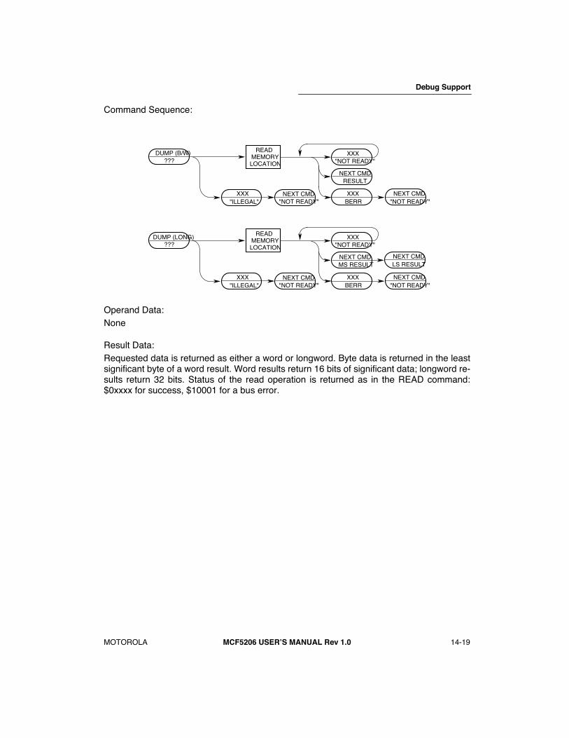
Debug Support
MOTOROLA MCF5206 USERÕS MANUAL Rev 1.0 14-19
Command Sequence:
Operand Data:None
Result Data:Requested data is returned as either a word or longword. Byte data is returned in the leastsignificant byte of a word result. Word results return 16 bits of significant data; longword re-sults return 32 bits. Status of the read operation is returned as in the READ command:$0xxxx for success, $10001 for a bus error.
XXX"NOT READY"
NEXT CMD RESULT
XXXBERR
XXX"ILLEGAL"
NEXT CMD"NOT READY"
NEXT CMD"NOT READY"
READ�MEMORY�LOCATION
DUMP (B/W)???
XXX"NOT READY"
NEXT CMD MS RESULT
XXXBERR
XXX"ILLEGAL"
NEXT CMD"NOT READY"
NEXT CMD"NOT READY"
READ�MEMORY�LOCATION
DUMP (LONG)???
NEXT CMDLS RESULT
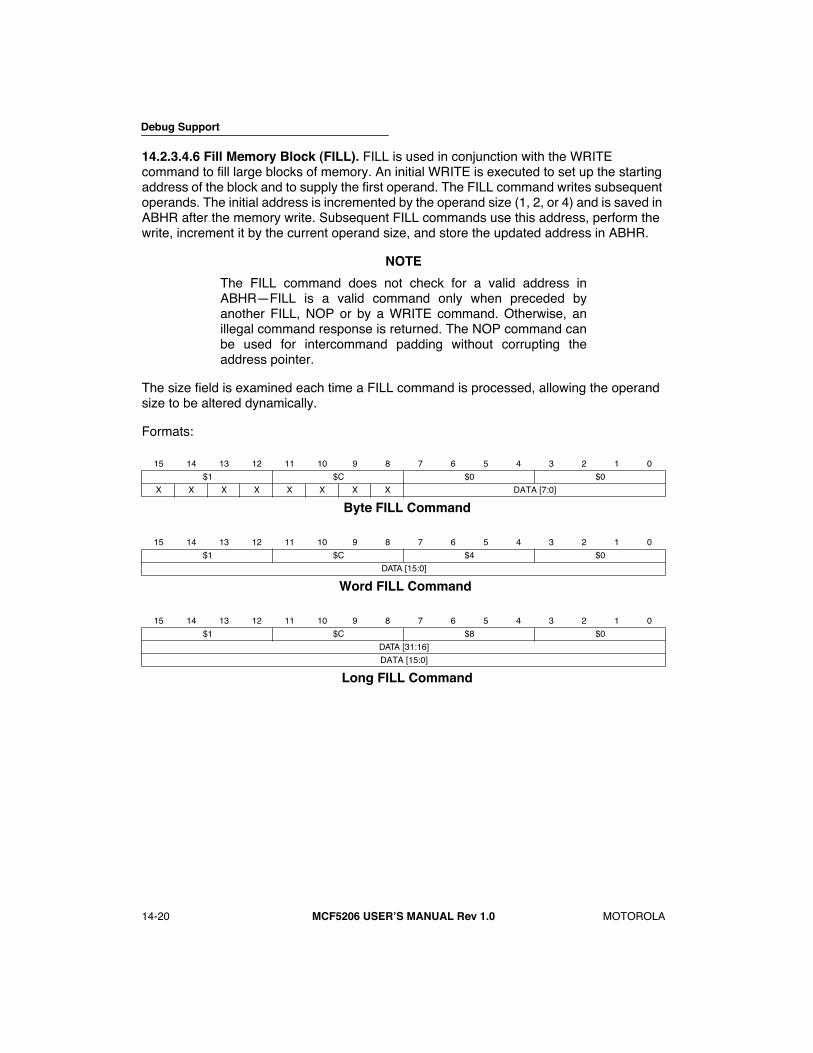
Debug Support
14-20 MCF5206 USERÕS MANUAL Rev 1.0 MOTOROLA
14.2.3.4.6 Fill Memory Block (FILL). FILL is used in conjunction with the WRITE command to fill large blocks of memory. An initial WRITE is executed to set up the starting address of the block and to supply the first operand. The FILL command writes subsequent operands. The initial address is incremented by the operand size (1, 2, or 4) and is saved in ABHR after the memory write. Subsequent FILL commands use this address, perform the write, increment it by the current operand size, and store the updated address in ABHR.
NOTE
The FILL command does not check for a valid address inABHRÑFILL is a valid command only when preceded byanother FILL, NOP or by a WRITE command. Otherwise, anillegal command response is returned. The NOP command canbe used for intercommand padding without corrupting theaddress pointer.
The size field is examined each time a FILL command is processed, allowing the operand size to be altered dynamically.
Formats:
15 14 13 12 11 10 9 8 7 6 5 4 3 2 1 0
$1 $C $0 $0
X X X X X X X X DATA [7:0]
Byte FILL Command
15 14 13 12 11 10 9 8 7 6 5 4 3 2 1 0
$1 $C $4 $0
DATA [15:0]
Word FILL Command
15 14 13 12 11 10 9 8 7 6 5 4 3 2 1 0
$1 $C $8 $0
DATA [31:16]
DATA [15:0]
Long FILL Command
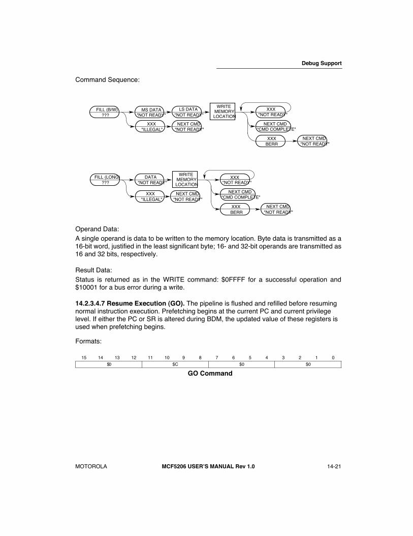
Debug Support
MOTOROLA MCF5206 USERÕS MANUAL Rev 1.0 14-21
Command Sequence:
Operand Data:A single operand is data to be written to the memory location. Byte data is transmitted as a16-bit word, justified in the least significant byte; 16- and 32-bit operands are transmitted as16 and 32 bits, respectively.
Result Data:Status is returned as in the WRITE command: $0FFFF for a successful operation and$10001 for a bus error during a write.
14.2.3.4.7 Resume Execution (GO). The pipeline is flushed and refilled before resuming normal instruction execution. Prefetching begins at the current PC and current privilege level. If either the PC or SR is altered during BDM, the updated value of these registers is used when prefetching begins.
Formats:
15 14 13 12 11 10 9 8 7 6 5 4 3 2 1 0
$0 $C $0 $0
GO Command
NEXT CMD"NOT READY"
"NOT READY"
XXXBERR
"CMD COMPLETE"
DATA"NOT READY"
XXX
NEXT CMDXXX"ILLEGAL"
NEXT CMD"NOT READY"
FILL (LONG)???
WRITE�MEMORY�LOCATION
NEXT CMD"NOT READY"
XXX"NOT READY"
XXXBERR
"CMD COMPLETE"
MS DATA"NOT READY"
NEXT CMDXXX"ILLEGAL"
NEXT CMD"NOT READY"
LS DATA"NOT READY"
WRITE�MEMORY�LOCATION
FILL (B/W)???
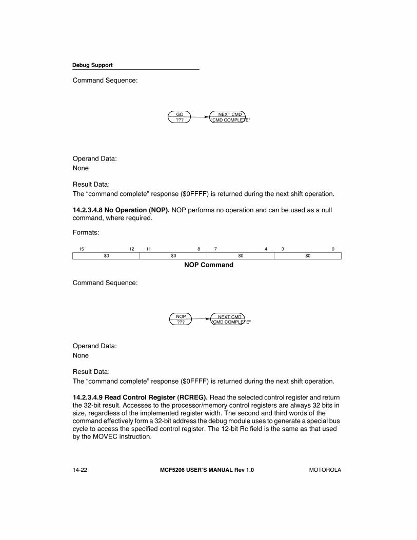
Debug Support
14-22 MCF5206 USERÕS MANUAL Rev 1.0 MOTOROLA
Command Sequence:
Operand Data:None
Result Data:The Òcommand completeÓ response ($0FFFF) is returned during the next shift operation.
14.2.3.4.8 No Operation (NOP). NOP performs no operation and can be used as a null command, where required.
Formats:
Command Sequence:
Operand Data:None
Result Data:The Òcommand completeÓ response ($0FFFF) is returned during the next shift operation.
14.2.3.4.9 Read Control Register (RCREG). Read the selected control register and return the 32-bit result. Accesses to the processor/memory control registers are always 32 bits in size, regardless of the implemented register width. The second and third words of the command effectively form a 32-bit address the debug module uses to generate a special bus cycle to access the specified control register. The 12-bit Rc field is the same as that used by the MOVEC instruction.
15 12 11 8 7 4 3 0
$0 $0 $0 $0
NOP Command
GO???
NEXT CMD"CMD COMPLETE"
NOP???
NEXT CMD�"CMD COMPLETE"

Debug Support
MOTOROLA MCF5206 USERÕS MANUAL Rev 1.0 14-23
Formats
Rc encoding:
Command Sequence:
Operand Data:The single operand is the 32-bit Rc control register select field.
Result Data:The contents of the selected control register are returned as a longword value. The data isreturned by most significant word first. For those control register widths less than 32 bits,only the implemented portion of the register is guaranteed to be correct. The remaining bits
15 14 13 12 11 10 9 8 7 6 5 4 3 2 1 0
$2 $9 $8 $0
$0 $0 $0 $0
$0 RC
RCREG Command
15 14 13 12 11 10 9 8 7 6 5 4 3 2 1 0
DATA [31:16]
DATA [15:0]
RCREG Result
Table 14-5. Control Register MapRc REGISTER DEFINITION
$002 Cache Control Register (CACR)$004 Access Control Unit 0 (ACR0)$005 Access Control Unit 1 (ACR1)$801 Vector Base Register (VBR)$80E Status Register (SR)$80F Program Counter (PC)$C04 RAM Base Address Register (RAMBAR)$C0F Module Base Address Register (MBAR)
EXT WORD"NOT READY"
EXT WORD"NOT READY"
RCREG???
NEXT CMD"NOT READY"
XXX"NOT READY"
XXX
XXXBERR
MS RESULT
READMEMORYLOCATION
NEXT CMDLS RESULT
XXX

Debug Support
14-24 MCF5206 USERÕS MANUAL Rev 1.0 MOTOROLA
of the longword are undefined. As an example, a read of the 16-bit SR returns the SR in thelower word and undefined data in the upper word.
14.2.3.4.10 Write Control Register (WCREG). The operand (longword) data is written to the specified control register. The write alters all 32 register bits.
Formats:
Command Sequence:
See Table 14-6 for Rc encodings.
Operand Data:Two operands are required for this instruction. The first long operand selects the register towhich the operand data is to be written. The second operand is the data.
Result Data:Successful write operations return a status of $0FFFF. Bus errors on the write cycle are in-dicated by the assertion of bit 16 in the status message and by a data pattern of $0001.
14.2.3.4.11 Read Debug Module Register (RDMREG). Read the selected Debug Module Register and return the 32-bit result. The only valid register selection for the RDMREG command is the CSR (DRc = $0).
15 14 13 12 11 10 9 8 7 6 5 4 3 2 1 0
$2 $8 $8 $0
$0 $0 $0 $0
$0 Rc
DATA [31:16]
DATA [15:0]
WCREG Command
EXT WORD"NOT READY"
EXT WORD"NOT READY"
WCREG???
NEXT CMD"NOT READY"
XXX"NOT READY"
XXX
XXXBERR
"CMD COMPLETENEXT CMD
WRITEMEMORYLOCATION
MS DATA"NOT READY"
LS DATA"NOT READY"

Debug Support
MOTOROLA MCF5206 USERÕS MANUAL Rev 1.0 14-25
Command Formats:
DRc encoding:
Command Sequence:
Operand Data:None
Result Data:The contents of the selected debug register are returned as a longword value. The data isreturned most significant word first.
14.2.3.4.12 Write Debug Module Register (WDMREG). The operand (longword) data is written to the specified Debug Module Register. All 32 bits of the register are altered by the write. The DSCLK signal must be inactive while CPU execution of the WDEBUG instruction is performed.
15 14 13 12 11 10 9 8 7 6 5 4 3 2 1 0
$2 $D $8 DRc
RDMREG BDM Command
15 14 13 12 11 10 9 8 7 6 5 4 3 2 1 0
DATA [31:16]
DATA [15:0]
RDMREG BDM Result
Table 14-6. Definition of DRc Encoding - Read
DRC[3:0] DEBUG REGISTER DEFINITION MNEMONICINITIAL STATE
$0 Configuration/Status CSR $0
$1-$F Reserved - Ð
XXXMS RESULT
XXX"ILLEGAL"
NEXT CMDLS RESULT
NEXT CMD"NOT READY"
RDMREG???
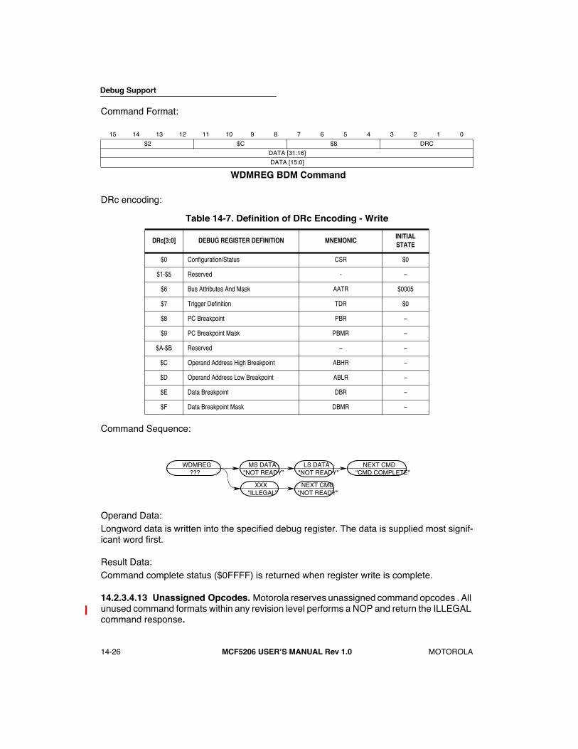
Debug Support
14-26 MCF5206 USERÕS MANUAL Rev 1.0 MOTOROLA
Command Format:
DRc encoding:
Command Sequence:
Operand Data:Longword data is written into the specified debug register. The data is supplied most signif-icant word first.
Result Data:Command complete status ($0FFFF) is returned when register write is complete.
14.2.3.4.13 Unassigned Opcodes. Motorola reserves unassigned command opcodes . All unused command formats within any revision level performs a NOP and return the ILLEGAL command response.
15 14 13 12 11 10 9 8 7 6 5 4 3 2 1 0
$2 $C $8 DRC
DATA [31:16]
DATA [15:0]
WDMREG BDM Command
Table 14-7. Definition of DRc Encoding - Write
DRc[3:0] DEBUG REGISTER DEFINITION MNEMONICINITIAL STATE
$0 Configuration/Status CSR $0
$1-$5 Reserved - Ð
$6 Bus Attributes And Mask AATR $0005
$7 Trigger Definition TDR $0
$8 PC Breakpoint PBR Ð
$9 PC Breakpoint Mask PBMR Ð
$A-$B Reserved Ð Ð
$C Operand Address High Breakpoint ABHR Ð
$D Operand Address Low Breakpoint ABLR Ð
$E Data Breakpoint DBR Ð
$F Data Breakpoint Mask DBMR Ð
MS DATA"NOT READY"
XXX"ILLEGAL"
LS DATA"NOT READY"
NEXT CMD"NOT READY"
WDMREG???
NEXT CMD"CMD COMPLETE"

Debug Support
MOTOROLA MCF5206 USERÕS MANUAL Rev 1.0 14-27
14.3 REAL-TIME DEBUG SUPPORTColdFire processors provide support for the debug of real-time applications. For these types of embedded systems, the processor cannot be halted during debug but must continue to operate. The foundation of this area of debug support is that while the processor cannot be halted to allow debugging, the system can tolerate small intrusions into the real-time operation.
As discussed in the previous subsection, the debug module provides a number of hardware resources to support various hardware breakpoint functions. Specifically, three types of breakpoints are supported: PC with mask, operand address range, and data with mask. These three basic breakpoints can be configured into one- or two-level triggers with the exact trigger response also programmable.
14.3.1 Programming ModelIn addition to the existing BDM commands that provide access to the processorÕs registers
and the memory subsystem, the Debug module contains a number of registers to support the required functionality. All of these registers are treated as 32-bit quantities, regardless of the actual number of bits in the implementation. The registers, known as the Debug Control Registers (DRc), are addressed using a 4-bit value as part of two new BDM commands (WDREG, RDREG).
These registers are also accessible from the processorÕs supervisor programming model through the execution of the WDEBUG instruction (Figure 14-5 illustrates the debug module programming model). Thus, the breakpoint hardware within the debug module can be accessed by the external development system using the serial interface, or by the operating system running on the processor core. It is the responsibility of the software to guarantee that all accesses to these resources are serialized and logically consistent. The hardware
Figure 14-5. Debug Programming Model
ADDRESSBREAKPOINT REGISTERS
PC BREAKPOINTREGISTERS
DATA BREAKPOINTREGISTERS
ABLRABHR
PBRPBMR
DBMRDBR
TDR
15
0
31
TRIGGER DEFINITIONREGISTER
ADDRESS ATTRIBUTETRIGGER REGISTERAATR
7
0
15
CSRCONFIGURATION/STATUSREGISTER
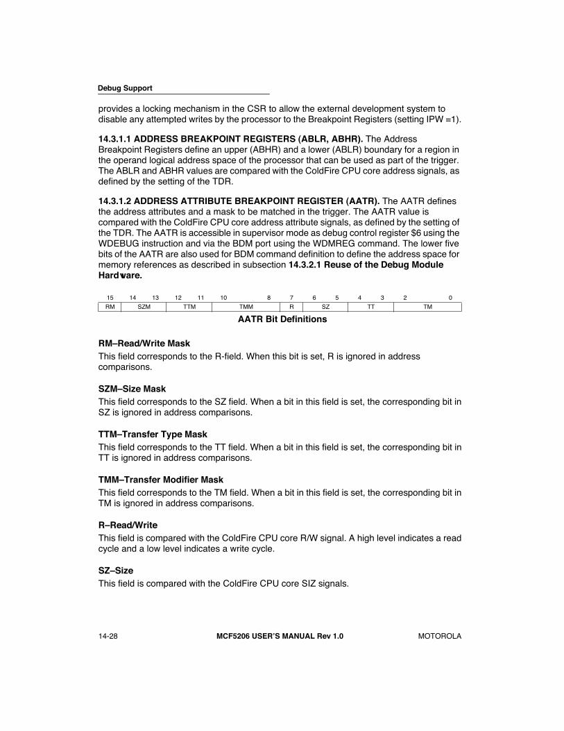
Debug Support
14-28 MCF5206 USERÕS MANUAL Rev 1.0 MOTOROLA
provides a locking mechanism in the CSR to allow the external development system to disable any attempted writes by the processor to the Breakpoint Registers (setting IPW =1).
14.3.1.1 ADDRESS BREAKPOINT REGISTERS (ABLR, ABHR). The Address Breakpoint Registers define an upper (ABHR) and a lower (ABLR) boundary for a region in the operand logical address space of the processor that can be used as part of the trigger. The ABLR and ABHR values are compared with the ColdFire CPU core address signals, as defined by the setting of the TDR.
14.3.1.2 ADDRESS ATTRIBUTE BREAKPOINT REGISTER (AATR). The AATR defines the address attributes and a mask to be matched in the trigger. The AATR value is compared with the ColdFire CPU core address attribute signals, as defined by the setting of the TDR. The AATR is accessible in supervisor mode as debug control register $6 using the WDEBUG instruction and via the BDM port using the WDMREG command. The lower five bits of the AATR are also used for BDM command definition to define the address space for memory references as described in subsection 14.3.2.1 Reuse of the Debug Module Hardware.
RMÐRead/Write MaskThis field corresponds to the R-field. When this bit is set, R is ignored in address comparisons.
SZMÐSize MaskThis field corresponds to the SZ field. When a bit in this field is set, the corresponding bit inSZ is ignored in address comparisons.
TTMÐTransfer Type MaskThis field corresponds to the TT field. When a bit in this field is set, the corresponding bit inTT is ignored in address comparisons.
TMMÐTransfer Modifier MaskThis field corresponds to the TM field. When a bit in this field is set, the corresponding bit inTM is ignored in address comparisons.
RÐRead/WriteThis field is compared with the ColdFire CPU core R/W signal. A high level indicates a readcycle and a low level indicates a write cycle.
SZÐSizeThis field is compared with the ColdFire CPU core SIZ signals.
15 14 13 12 11 10 8 7 6 5 4 3 2 0
RM SZM TTM TMM R SZ TT TM
AATR Bit Definitions

Debug Support
MOTOROLA MCF5206 USERÕS MANUAL Rev 1.0 14-29
SZÑ-SizeThis field is compared to the ColdFire CPU core SIZ signals. These signals indicate the datasize for the bus transfer. Table 14-8 shows the definitions for the SZ encodings.
TTÐTransfer TypeThis field is compared with the ColdFire CPU core TT signals. These signals indicate thetransfer type for the bus transfer. Table 14-9 shows the definition of the TT encodings.
TMÐTransfer ModifierThis field is compared with the ColdFire CPU core TM signals. These signals provide sup-plemental information for each transfer type. Table 14-10 shows encodings for normal trans-fers and Table 14-11 shows the encodings for alternate and debug access transfers. Forinterrupt-acknowledge transfers, the TM [2:0] signals indicate the interrupt level being acknowledged. For CPU space transfers initiated by a MOVEC instruction or a debug
Table 14-8. SZ Encodings
SZ[1:0] TRANSFER SIZE
00 Longword (4 bytes)
01 Byte
10 Word (2 bytes)
11 Line (4 x 4 bytes)
Table 14-9. Transfer Type Encodings
TT[1:0] TRANSFER TYPE
00 Normal Access
01 Reserved
10 Alternate and Debug Access
11 Acknowledge Access
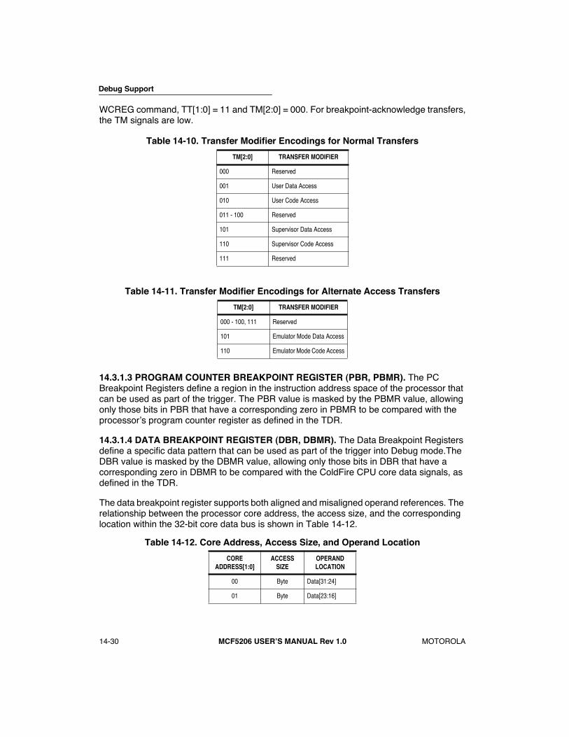
Debug Support
14-30 MCF5206 USERÕS MANUAL Rev 1.0 MOTOROLA
WCREG command, TT[1:0] = 11 and TM[2:0] = 000. For breakpoint-acknowledge transfers,the TM signals are low.
14.3.1.3 PROGRAM COUNTER BREAKPOINT REGISTER (PBR, PBMR). The PC Breakpoint Registers define a region in the instruction address space of the processor that can be used as part of the trigger. The PBR value is masked by the PBMR value, allowing only those bits in PBR that have a corresponding zero in PBMR to be compared with the processorÕs program counter register as defined in the TDR.
14.3.1.4 DATA BREAKPOINT REGISTER (DBR, DBMR). The Data Breakpoint Registers define a specific data pattern that can be used as part of the trigger into Debug mode.The DBR value is masked by the DBMR value, allowing only those bits in DBR that have a corresponding zero in DBMR to be compared with the ColdFire CPU core data signals, as defined in the TDR.
The data breakpoint register supports both aligned and misaligned operand references. The relationship between the processor core address, the access size, and the corresponding location within the 32-bit core data bus is shown in Table 14-12.
Table 14-10. Transfer Modifier Encodings for Normal Transfers
TM[2:0] TRANSFER MODIFIER
000 Reserved
001 User Data Access
010 User Code Access
011 - 100 Reserved
101 Supervisor Data Access
110 Supervisor Code Access
111 Reserved
Table 14-11. Transfer Modifier Encodings for Alternate Access Transfers
TM[2:0] TRANSFER MODIFIER
000 - 100, 111 Reserved
101 Emulator Mode Data Access
110 Emulator Mode Code Access
Table 14-12. Core Address, Access Size, and Operand Location
CORE ADDRESS[1:0]
ACCESS SIZE
OPERAND LOCATION
00 Byte Data[31:24]
01 Byte Data[23:16]
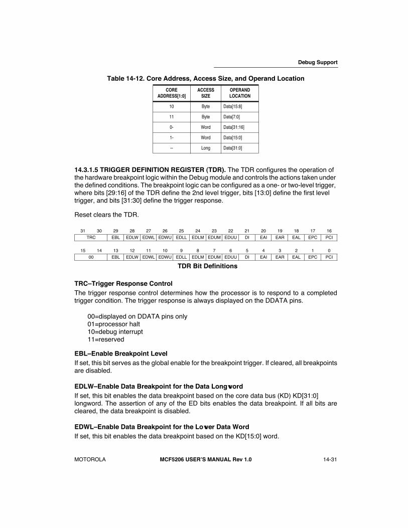
Debug Support
MOTOROLA MCF5206 USERÕS MANUAL Rev 1.0 14-31
14.3.1.5 TRIGGER DEFINITION REGISTER (TDR). The TDR configures the operation of the hardware breakpoint logic within the Debug module and controls the actions taken under the defined conditions. The breakpoint logic can be configured as a one- or two-level trigger, where bits [29:16] of the TDR define the 2nd level trigger, bits [13:0] define the first level trigger, and bits [31:30] define the trigger response.
Reset clears the TDR.
TRCÐTrigger Response ControlThe trigger response control determines how the processor is to respond to a completedtrigger condition. The trigger response is always displayed on the DDATA pins.
00=displayed on DDATA pins only01=processor halt10=debug interrupt11=reserved
EBLÐEnable Breakpoint LevelIf set, this bit serves as the global enable for the breakpoint trigger. If cleared, all breakpointsare disabled.
EDLWÐEnable Data Breakpoint for the Data LongwordIf set, this bit enables the data breakpoint based on the core data bus (KD) KD[31:0] longword. The assertion of any of the ED bits enables the data breakpoint. If all bits arecleared, the data breakpoint is disabled.
EDWLÐEnable Data Breakpoint for the Lower Data WordIf set, this bit enables the data breakpoint based on the KD[15:0] word.
10 Byte Data[15:8]
11 Byte Data[7:0]
0- Word Data[31:16]
1- Word Data[15:0]
-- Long Data[31:0]
31 30 29 28 27 26 25 24 23 22 21 20 19 18 17 16
TRC EBL EDLW EDWL EDWU EDLL EDLM EDUM EDUU DI EAI EAR EAL EPC PCI
15 14 13 12 11 10 9 8 7 6 5 4 3 2 1 0
00 EBL EDLW EDWL EDWU EDLL EDLM EDUM EDUU DI EAI EAR EAL EPC PCI
TDR Bit Definitions
Table 14-12. Core Address, Access Size, and Operand Location
CORE ADDRESS[1:0]
ACCESS SIZE
OPERAND LOCATION

Debug Support
14-32 MCF5206 USERÕS MANUAL Rev 1.0 MOTOROLA
EDWUÐEnable Data Breakpoint for the Upper Data WordIf set, this bit enables the data breakpoint trigger based on the KD[31:16] word.
EDLLÐEnable Data Breakpoint for the Lower Lower Data ByteIf set, this bit enables the data breakpoint trigger based on the KD[7:0] byte.
EDLMÐEnable Data Breakpoint for the Lower Middle Data ByteIf set, this bit enables the data breakpoint trigger based on the KD[15:8] byte.
EDUMÐEnable Data Breakpoint for the Upper Middle Data ByteIf set, this bit enables the data breakpoint trigger based on the KD[23:16] byte.
EDUUÐEnable Data Breakpoint for the Upper Upper Data ByteIf set, this bit enables the data breakpoint trigger based on the KD[31:24] byte.
DIÐData Breakpoint InvertThis bit provides a mechanism to invert the logical sense of all the data breakpoint compar-ators. This can develop a trigger based on the occurrence of a data value not equal to theone programmed into the DBR.
The assertion of any of the EA bits enables the address breakpoint. If all three bits arecleared, this breakpoint is disabled.
EAIÐEnable Address Breakpoint InvertedIf set, this bit enables the address breakpoint based outside the range defined by ABLR andABHR.
EARÐEnable Address Breakpoint RangeIf set, this bit enables the address breakpoint based on the inclusive range defined by ABLRand ABHR.
EALÐEnable Address Breakpoint LowIf set, this bit enables the address breakpoint based on the address contained in the ABLR.
EPCÐEnable PC BreakpointIf set, this bit enables the PC breakpoint. Clearing this bit disables the PC breakpoint.
PCIÐPC Breakpoint InvertIf set, this bit allows execution outside a given region as defined by PBR and PBMR to en-able a trigger. If cleared, the PC breakpoint is defined within the region defined by PBR andPBMR.
14.3.1.6 CONFIGURATION/STATUS REGISTER (CSR). The Configuration/Status Register defines the operating configuration for the processor and memory subsystem. In

Debug Support
MOTOROLA MCF5206 USERÕS MANUAL Rev 1.0 14-33
addition to defining the microprocessor configuration, this register also contains status information from the breakpoint logic. The CSR is cleared during system reset. The CSR can
be read and written by the external development system and written by the supervisor programming model.
StatusÐBreakpoint StatusThis 4-bit field defines provides read-only status information concerning the hardwarebreakpoints. This field is defined as follows:
$0 = no breakpoints enabled$1 = waiting for level 1 breakpoint$2 = level 1 breakpoint triggered$5 = waiting for level 2 breakpoint$6 = level 2 breakpoint triggered
The CSR[30-28] bits are translated and output on the DDATA[3:1] signals where x is theDDATA[0] bit.
000x = no breakpoints enabled001x = waiting for level 1 breakpoint010x = level 1 breakpoint triggered101x = waiting for level 2 breakpoint110x = level 2 breakpoint triggered
This breakpoint status is also output on the DDATA port when the bus is not displaying Cold-Fire CPU core captured data. A write to the TDR resets this field.
FOFÐFault-on-FaultIf this read-only status bit is set, a catastrophic halt has occurred and forced entry into BDM.This bit is cleared on a read of the CSR.
TRGÐHardware Breakpoint TriggerIf this read-only status bit is set, a hardware breakpoint has halted the processor core andforced entry into BDM. This bit is cleared on a read from the CSR or when the processor isrestarted.
31 28 27 26 25 24 23 17 16
STATUS FOF TRG HALT BKPT RESERVED IPW
15 14 13 12 11 10 9 8 7 6 5 4 3 2 1 0
MAP TRC EMU DDC UHE BTB 0 NPL IPI SSM 0 0 0 0
CSR Bit Definitions

Debug Support
14-34 MCF5206 USERÕS MANUAL Rev 1.0 MOTOROLA
HaltÐProcessor HaltIf this read-only status bit is set, the processor has executed the HALT instruction and forcedentry into BDM. This bit is cleared on a read from the CSR or when the processor is restarted.
BKPTÐBKPT AssertIf this read-only status bit is set, the BKPT signal was asserted, forcing the processor intoBDM. This bit is cleared on a read from the CSR or when the processor is restarted.
IPWÐInhibit Processor Writes to Debug RegistersIf set, this bit inhibits any processor-initiated writes to the debug moduleÕs programmingmodel registers. This bit can be modified only by commands from the external developmentsystem.
MAPÐForce Processor References in Emulator ModeIf set, this bit forces the processor to map all references while in emulator mode to a specialaddress space, TT = 10, TM = 101 (data) and 110 (text). If cleared, all emulator-mode ref-erences are mapped into supervisor text and data spaces.
TRCÐForce Emulation Mode on Trace ExceptionIf set, this bit forces the processor to enter emulator mode when a trace exception occurs.
EMUÐForce Emulation ModeIf set, this bit forces the processor to begin execution in emulator mode. This bit is examinedonly when RSTI is negated, as the processor begins reset exception processing.
DDCÐDebug Data ControlThis 2-bit field provides configuration control for capturing operand data for display on theDDATA port. The encoding is as follows:
00 = no operand data is displayed01 = capture all M-Bus write data10 = capture all M-Bus read data11 = capture all M-Bus read and write data
In all cases, the DDATA port displays the number of bytes defined by the operand referencesize, i.e., byte displays 8 bits, word displays 16 bits, and long displays 32 bits.
UHE-User Halt EnableThis bit selects the CPU privilege level required to execute the HALT instruction.
0 = HALT is a privileged, supervisor-only instruction1 = HALT is a nonprivileged, supervisor/user instruction

Debug Support
MOTOROLA MCF5206 USERÕS MANUAL Rev 1.0 14-35
BTBÐBranch Target BytesThis 2-bit field defines the number of bytes of branch target address to be displayed on theDDATA outputs. The encoding is as follows:
00 = 0 bytes01 = lower two bytes of the target address10 = lower three bytes of the target address11 = entire four-byte target address
The bytes are always displayed in a least-significant-to-most-significant order. The proces-sor captures only those target addresses associated with taken branches using a variant ad-dressing mode. This includes JMP and JSR instructions using address register indirect orindexed addressing modes, all RTE and RTS instructions as well as all exception vectors.
NPLÐNonpipelined ModeIf set, this bit forces the processor core to operate in a nonpipeline mode of operation. In thismode, the processor effectively executes a single instruction at a time with no overlap.
IPIÐIgnore Pending InterruptsIf set, this bit forces the processor core to ignore any pending interrupt requests signalledon KIPL[2:0] while executing in single-instruction-step mode.
SSMÐSingle-Step ModeIf set, this bit forces the processor core to operate in a single-instruction-step mode. Whilein this mode, the processor executes a single instruction and then halts. While halted, anyof the BDM commands can be executed. On receipt of the GO command, the processor ex-ecutes the next instruction and then halts again. This process continues until the single-in-struction-step mode is disabled.
ReservedAll bits labeled Reserved or Ò0Ó are currently unused and reserved for future use. These bitsshould always be written as 0.
14.3.2 Theory of OperationThe breakpoint hardware can be configured to respond to triggers in several ways. The preferred response is programmed into the Trigger Definition Register. In all situations where a breakpoint triggers, an indication is provided on the DDATA output port (when not displaying captured operands or branch addresses) as shown in Table 14-13.

Debug Support
14-36 MCF5206 USERÕS MANUAL Rev 1.0 MOTOROLA
The breakpoint status is also posted in the CSR.
The new BDM instructions load and configure the desired breakpoints using the appropriate registers. As the system operates, a breakpoint trigger generates a response as defined in the TDR. If the system can tolerate the processor being halted, a BDM entry can be used. With the TRC bits of the TDR = 01, the breakpoint trigger halts the core (as reflected in the PST = $F status). For PC breakpoints, the halt occurs before the targeted instruction is executed. For address and data breakpoints, the processor may have executed several additional instructions. For these breakpoints, trigger reporting is imprecise.
If the processor core cannot be halted, the special debug interrupt can be used. With this configuration, TRC bits of the TDR = 10, the breakpoint trigger is converted into a debug interrupt to the processor. This interrupt is treated as higher than the nonmaskable level 7 interrupt request. As with all interrupts, it is made pending the processor samples, once per instruction. Again, the hardware forces the PC breakpoint to occur immediately (before the execution of the targeted instruction). This is possible because the PC breakpoint comparison is enabled at the same time the interrupt sampling occurs. For the address and data breakpoints, the reporting is imprecise.
Once the debug interrupt is recognized, the processor aborts execution and initiates exception processing. At the initiation of the exception processing, the core enters emulator mode. Depending on the state of the MAP bit in the CSR, this mode could force all memory accesses (including the exception stack frame writes and the vector fetch) into a specially mapped address space signalled by TT = 2, TM = {5, 6}. After the standard 8-byte exception stack is created, the processor fetches a unique exception vector (offset $030) from the vector table.
Execution continues at the instruction address contained in this exception vector. All interrupts are ignored while in emulator mode. You can program the debug-interrupt handler to perform the necessary context saves using the supervisor instruction set. As an example, this handler may save the state of all the program-visible registers as well as the current context into a reserved memory area.
Table 14-13. DDATA, CSR[31:28] Breakpoint Response
DDATA[3:0], CSR[31:28]
BREAKPOINT STATUS
000x, $0 No breakpoints enabled
001x, $1 Waiting for Level 1 breakpoint
010x, $2 Level 1 breakpoint triggered
011x-100x, $3-4 Reserved
101x, $5 Waiting for Level 2 breakpoint
110x, $6 Level 2 breakpoint triggered
111x, $7-$F Reserved

Debug Support
14-37 MCF5206 USERÕS MANUAL Rev 1.0 MOTOROLA
Once the required operations are completed, the return-from-exception (RTE) instruction is executed and the processor exits emulator mode. The processor status output port provides a unique encoding for emulator mode entry ($D) and exit ($7). Once the debug interrupt handler has completed its execution, the external development system can then access the reserved memory locations using the BDM commands to read memory.
14.3.2.1 REUSE OF THE DEBUG MODULE HARDWARE. The Debug module implementation provides a common hardware structure for both BDM and breakpoint functionality. Several structures are used for both BDM and breakpoint purposes. Table 14-14 identifies the shared hardware structures.
The shared use of these hardware structures means the loading of the register to perform any specified function is destructive to the shared function. For example, if an operand address breakpoint is loaded into the debug module, a BDM command to access memory overwrites the breakpoint. If a data breakpoint is configured, a BDM write command overwrites the breakpoint contents.
14.3.3 Concurrent BDM and Processor OperationThe debug module supports concurrent operation of both the processor and most BDM commands. BDM commands can be executed while the processor is running, except for the operations that access processor/memory registers:
¥ Read/Write Address and Data Registers
¥ Read/Write Control Registers
For BDM commands that access memory, the debug module requests the ColdFire coreÕs bus. The processor responds by stalling the instruction fetch pipeline and then waiting until all current core bus activity is complete. At that time, the processor relinquishes the core bus to allow the debug module to perform the required operation. After the conclusion of the debug module core bus cycle, the processor reclaims ownership of the core bus.
The development system must be careful when configuring the Breakpoint Registers if the processor is executing. The debug module does not contain any hardware interlocks; therefore Motorola recommends that the TDR be disabled while the Breakpoint Registers are being loaded. At the conclusion of this process, the TDR can be written to define the exact trigger. This approach guarantees that no spurious breakpoint triggers occur.
Because there are no hardware interlocks in the debug unit, no BDM operations are allowed while the CPU is writing the Debug Registers (SDSCLK must be inactive).
Table 14-14. Shared BDM/Breakpoint Hardware
REGISTER BDM FUNCTION BREAKPOINT FUNCTION
AATR Bus attributes for all memory commands Attributes for address breakpoint
ABHR Address for all memory commands Address for address breakpoint
DBR Data for all BDM write commands Data for data breakpoint

Debug Support
14-38 MCF5206 USERÕS MANUAL Rev 1.0 MOTOROLA
14.4 MOTOROLA RECOMMENDED BDM PINOUTThe ColdFire BDM connector is a 26-pin Berg connector arranged 2x13, shown in Figure 14-6.
NOTES:1 Supplied by target2 Pins reserved for BDM developer use. Contact developer.* Denotes a vectored signal
Figure 14-6. 26-Pin Berg Connector Arranged 2x13
14.4.1 Differences Between the ColdFire BDM and a CPU32 BDM1. DSCLK, BKPT, and DSDI must meet the setup and hold times relative to the rising
edge of the processor clock to prevent the processor from propagating metastable states.
2. DSO transitions relative to the rising edge of DSCLK only. In the CPU32 BDM, DSO transitions between serial transfers to indicate to the development system that a com-mand has successfully completed. The ColdFire BDM does not support this feature.
3. The development system must note that the DSO is not valid during the first rising edge of DSCLK. Instead, the first rising edge of DSCLK causes DSO to transmit the MSB of DSO. A serial transfer is illustrated in Figure 14-7.
1
3
5
7
9
11
13
15
17
19
21
23
25
2
4
6
8
10
12
14
16
18
20
22
24
26
DEVELOPER RESERVED 2
GND
GND
RESET*
+5V1
GND
PST2
PST0
DDATA2
DDATA0*
MOTOROLA RESERVED
GND
VCC_CPU
BKPT
DSCLK
DEVELOPER RESERVED 2
DSI
DSO
PST3*
PST1
DDATA3*
DDATA1
GND
MOTOROLA RESERVED
CLK_CPU
TEA
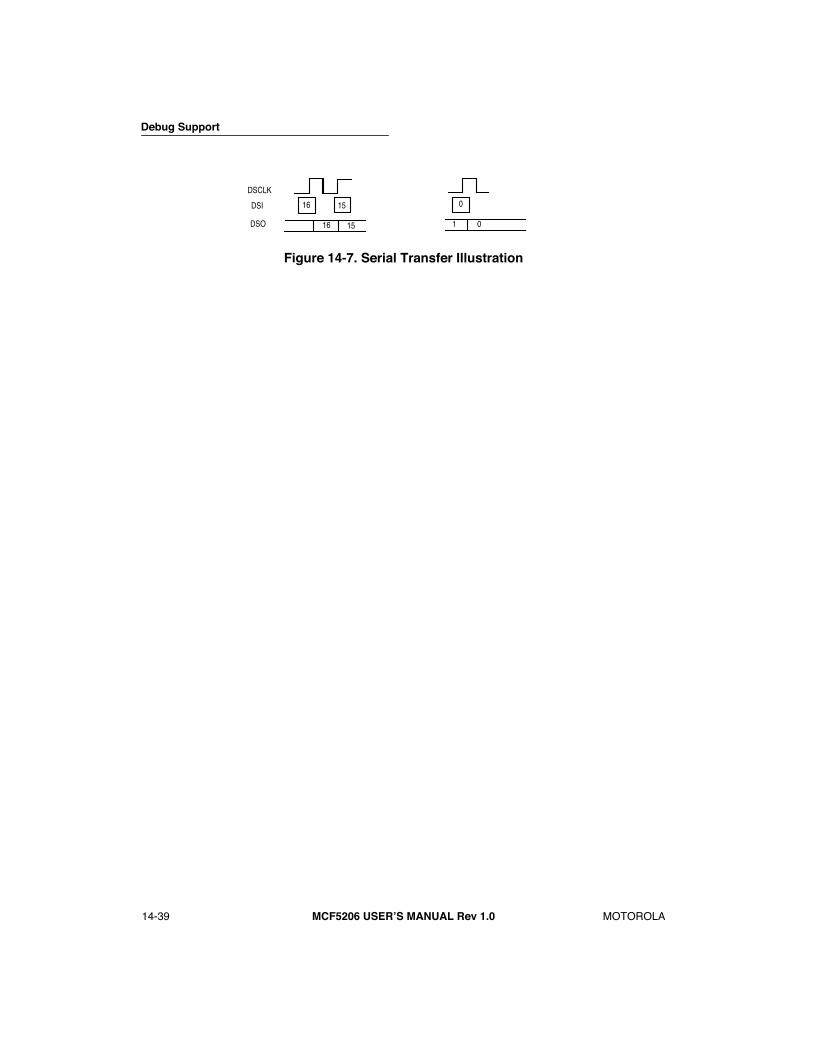
Debug Support
14-39 MCF5206 USERÕS MANUAL Rev 1.0 MOTOROLA
Figure 14-7. Serial Transfer Illustration
16 15 0
16 15 1 0
DSCLK
DSI
DSO

MOTOROLA
MCF5206 USERÕS MANUAL Rev 1.0
15-1
SECTION 15IEEE 1149.1 TEST ACCESS PORT (JTAG)
The MCF5206 includes dedicated user-accessible test logic that is fully compliant with the IEEE standard 1149.1
Standard Test Access Port and Boundary Scan Architecture
. Use the following description in conjunction with the supporting IEEE document listed above. This section includes the description of those chip-specific items that the IEEE standard requires as well as those items specific to the MCF5206 implementation.
The MCF5206 JTAG test architecture implementation currently supports circuit board test strategies that are based on the IEEE standard. This architecture provides access to all of the data and chip control pins from the board edge connector through the standard four-pin test access port (TAP) and the active-low JTAG reset pin, TRST. The test logic itself uses a static design and is wholly independent of the system logic, except where the JTAG is subordinate to other complimentary test modes (see the
Debug Support
section for more information). When in subordinate mode, the JTAG test logic is placed in reset and the TAP pins can be used for other purposes in accordance with the rules and restrictions set forth using a JTAG compliance-enable pin.
The MCF5206 JTAG implementation can:
¥ Perform boundary-scan operations to test circuit board electrical continuity
¥ Bypass the MCF5206 device by reducing the shift register path to a single cell
¥ Sample the MCF5206 system pins during operation and transparently shift out the result
¥ Set the MCF5206 output drive pins to fixed logic values while reducing the shift register path to a single cell
¥ Protect the MCF5206 system output and input pins from backdriving and random toggling (such as during in-circuit testing) by placing all system signal pins to high- impedance state
NOTE
The IEEE Standard 1149.1 test logic cannot be consideredcompletely benign to those planning not to use JTAG capability.You must observe certain precautions to ensure that this logicdoes not interfere with system or debug operation. Refer toSection 15.6 Disabling the IEEE 1149.1 Standard Operation.
DATE: 9-2-98
REVISION NO.: 1.1
PAGES AFFECTED: SEE CHANGE BARS

IEEE 1149.1 Test Access Port (JTAG)
15-2
MCF5206 USERÕS MANUAL Rev 1.0
MOTOROLA
15.1 OVERVIEW
Figure 15-1 is a block diagram of the MCF5206 implementation of the 1149.1 IEEE Standard. The test logic includes several test data registers, an instruction register, instruction register control decode, and a 16-state dedicated TAP controller.
Figure 15-1. JTAG Test Logic Block Diagram
15.2 JTAG PIN DESCRIPTIONS
The MCF5206 JTAG pin is defined to be a compliance-enable input per Section 3.8 of the IEEE Standard 1149.1a-1993 entitled ÒSubordination of this Standard within a Higher Level Test Strategy.Ó When JTAG is a logic 0, the MCF5206 is in JTAG mode; when JTAG is a logic 1, the MCF5206 is in debug mode.
BYPASS
3-BIT INSTRUCTION DECODE
3-BIT INSTRUCTION REGISTER
MUX
TAPCONTROLLER
TEST DATA REGISTERS
TDI
TMS
TCK
TRST
TDO
V+
BOUNDARY SCAN REGISTER
IDCODE REGISTER
MUX
V+
V+

IEEE 1149.1 Test Access Port (JTAG)
MOTOROLA
MCF5206 USERÕS MANUAL Rev 1.0
15-3
When the compliance-enable state is set for JTAG mode, the pin descriptions in Table 15-1 apply.
15.3 JTAG REGISTER DESCRIPTIONS
15.3.1 JTAG Instruction Shift Register
The MCF5206 IEEE 1149.1 Standard implementation uses a 3-bit instruction-shift register without parity. This register transfers its value to a parallel hold register and applies one of six possible instructions on the falling edge of TCK when the TAP state machine is in the update-IR state. To load the instructions into the shift portion of the register, place the serial data on the TDI pin prior to each rising edge of TCK. The MSB of the instruction shift register is the bit closest to the TDI pin and the LSB is the bit closest to the TDO pin.
Table 15-2 lists the public customer-usable instructions that are supported along with their encoding.
The IEEE 1149.1 Standard requires the EXTEST, SAMPLE/PRELOAD, and BYPASS instructions. IDCODE, CLAMP and HIGHZ are optional standard instructions that the MCF5206 implementation supports and are described in the 1149.1.
15.3.1.1 EXTEST INSTRUCTION.
The external test instruction (EXTEST) selects the boundary-scan register. The EXTEST instruction forces all output pins and bidirectional pins configured as outputs to the preloaded fixed values (with the SAMPLE/PRELOAD instruction) and held in the boundary-scan update registers. The EXTEST instruction can
Table 15-1. JTAG Pin Descriptions
PIN DESCRIPTION
TCK A test clock input that synchronizes test logic operationsTMS A test mode select input with a default internal pullup resistor that is sampled on the rising edge of TCK to
sequence the TAP controllerTDI A serial test data input with a default internal pullup resistor that is sampled on the rising edge of TCKTDO A three-state test data output that is actively driven only in the Shift-IR and Shift-DR controller states and only
updates on the falling edge of TCK TRST An active-low asynchronous reset with a default internal pullup resistor that forces the TAP controller into the
test-logic-reset state.
Table 15-2. JTAG Instructions
INSTRUCTION ABBR CLASS IR[2:0] INSTRUCTION SUMMARY
EXTEST EXT Required 000 Select BS register while applying fixed values to output pins and asserting functional reset
IDCODE IDC Optional 001 Selects IDCODE register for shiftSAMPLE/PRELOAD
SMP Required 100 Selects BS register for shift, sample, and preload without disturbing functional operation
HIGHZ HIZ Optional 101 Selects the bypass register while three-stating all output pins and asserting functional reset
CLAMP CMP Optional 110 Selects bypass while applying fixed values to output pins and asserting functional reset
BYPASS BYP Required 111 Selects the bypass register for data operations

IEEE 1149.1 Test Access Port (JTAG)
15-4
MCF5206 USERÕS MANUAL Rev 1.0
MOTOROLA
also configure the direction of bidirectional pins and establish high-impedance states on some pins. The EXTEST instruction becomes active on the falling edge of TCK in the update-IR state when the data held in the instruction-shift register is equivalent to octal 0.
15.3.1.2 IDCODE.
The IDCODE instruction selects the 32-bit IDcode register for connection as a shift path between the TDI pin and the TDO pin. This instruction lets you interrogate the MCF5206 to determine its version number and other part identification data. The IDcode register has been implemented in accordance with IEEE 1149.1 so that the least significant bit of the shift register stage is set to logic 1 on the rising edge of TCK following entry into the capture-DR state. Therefore, the first bit to be shifted out after selecting the IDcode register is always a logic 1. The remaining 31-bits are also set to fixed values (see 15.3.2 IDcode Register) on the rising edge of TCK following entry into the capture-DR state.
The IDCODE instruction is the default value placed in the instruction register when a JTAG reset is accomplished by either asserting TRST or holding TMS high while clocking TCK through at least five rising edges and the falling edge after the fifth rising edge. A JTAG reset causes the TAP state machine to enter the test-logic-reset state (normal operation of the TAP state machine into the test-logic-reset state also results in placing the default value of octal 1 into the instruction register). The shift register portion of the instruction register is loaded with the default value of octal 1 when in the Capture-IR state and a rising edge of TCK occurs.
15.3.1.3 SAMPLE/PRELOAD INSTRUCTION.
The SAMPLE/PRELOAD instruction provides two separate functions. First, it obtains a sample of the system data and control signals present at the MCF5206 input pins and just prior to the boundary scan cell at the output pins. This sampling occurs on the rising edge of TCK in the capture-DR state when an instruction encoding of octal 4 is resident in the instruction register. You can observe this sampled data by shifting it through the boundary-scan register to the output TDO by using the shift-DR state. Both the data capture and the shift operation are transparent to system operation. You are responsible for providing some form of external synchronization to achieve meaningful results because there is no internal synchronization between TCK and the system clock, CLK.
The second function of the SAMPLE/PRELOAD instruction is to initialize the boundary scan register update cells before selecting EXTEST or CLAMP. This is achieved by ignoring the data being shifted out of the TDO pin while shifting in initialization data. The update-DR state in conjunction with the falling edge of TCK can then transfer this data to the update cells. This data is applied to the external output pins when one of the instructions listed above is applied.
15.3.1.4 HIGHZ INSTRUCTION.
The HIGHZ instruction anticipates the need to backdrive the output pins and protect the input pins from random toggling during circuit board testing. The HIGHZ instruction selects the bypass register, forcing all output and bidirectional pins to the high-impedance state.

IEEE 1149.1 Test Access Port (JTAG)
MOTOROLA
MCF5206 USERÕS MANUAL Rev 1.0
15-5
The HIGHZ instruction goes active on the falling edge of TCK in the update-IR state when the data held in the instruction shift register is equivalent to octal 5.
15.3.1.5 CLAMP INSTRUCTION.
The CLAMP instruction selects the bypass register and asserts functional reset while simultaneously forcing all output pins and bidirectional pins conÞgured as outputs to the Þxed values that are preloaded and held in the boundary-scan update registers. This instruction enhances test efÞciency by reducing the overall shift path to a single bit (the bypass register) while conducting an EXTEST type of instruction through the boundary-scan register. The CLAMP instruction becomes active on the falling edge of TCK in the update-IR state when the data held in the instruction-shift register is equivalent to octal 6.
15.3.1.6 BYPASS INSTRUCTION.
The BYPASS instruction selects the single-bit bypass register, creating a single-bit shift register path from the TDI pin to the bypass register to the TDO pin. This instruction enhances test efficiency by reducing the overall shift path when a device other than the MCF5206 processor becomes the device under test on a board design with multiple chips on the overall 1149.1 defined boundary-scan chain. The bypass register has been implemented in accordance with 1149.1 so that the shift register stage is set to logic zero on the rising edge of TCK following entry into the capture-DR state. Therefore, the first bit to be shifted out after selecting the bypass register is always a logic zero (to differentiate a part that supports an IDCODE register from a part that supports only the bypass register). The BYPASS instruction goes active on the falling edge of TCK in the update-IR state when the data held in the instruction shift register is equivalent to octal 7.
15.3.2 IDcode Register
An IEEE 1149.1 compliant JTAG identification register has been included on the MCF5206. The MCF5206 JTAG instruction encoded as octal 1 provides for reading the JTAG IDcode register. The format of this register is defined below.
Bits 31-28 Version NumberIndicates the revision number of the MCF5206.
Bits 27-22 Design CenterIndicates the ColdFire design center.
Bits 21-12 Device NumberIndicates an MCF5206.
VERSION NO 0 1 0 0 1 1 0 0 0 0 0 0
31 30 29 28 27 26 25 24 23 22 21 20 19 18 17 16
0 0 0 1 0 0 0 0 0 0 0 1 1 1 0 1
15 14 13 12 11 10 9 8 7 6 5 4 3 2 1 0
ID code Register
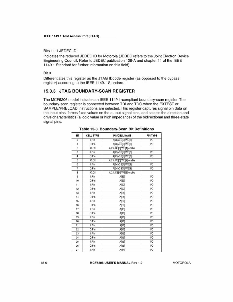
IEEE 1149.1 Test Access Port (JTAG)
15-6
MCF5206 USERÕS MANUAL Rev 1.0
MOTOROLA
Bits 11-1 JEDEC IDIndicates the reduced JEDEC ID for Motorola (JEDEC refers to the Joint Electron Device Engineering Council. Refer to JEDEC publication 106-A and chapter 11 of the IEEE 1149.1 Standard for further information on this field).
Bit 0Differentiates this register as the JTAG IDcode register (as opposed to the bypass register) according to the IEEE 1149.1 Standard.
15.3.3 JTAG BOUNDARY-SCAN REGISTER
The MCF5206 model includes an IEEE 1149.1-compliant boundary-scan register. The boundary-scan register is connected between TDI and TDO when the EXTEST or SAMPLE/PRELOAD instructions are selected. This register captures signal pin data on the input pins, forces Þxed values on the output signal pins, and selects the direction and drive characteristics (a logic value or high impedance) of the bidirectional and three-state signal pins.
Table 15-3. Boundary-Scan Bit Definitions
BIT CELL TYPE PIN/CELL NAME PIN TYPE
0 I.Pin A[26]/CS[6]/WE[1] I/O1 O.Pin A[26]/CS[6]/WE[1] I/O2 IO.Ctl A[26]/CS[6]/WE[1] enable -3 I.Pin A[25]/CS[5]/WE[2] I/O4 O.Pin A[25]/CS[5]/WE[2] I/O5 IO.Ctl A[25]/CS[5]/WE[2] enable -6 I.Pin A[24]/CS[4]/WE[3] I/O7 O.Pin A[24]/CS[4]/WE[3] I/O8 IO.Ctl A[24]/CS[4]/WE[3] enable -9 I.Pin A[23] I/O10 O.Pin A[23] I/O11 I.Pin A[22] I/O12 O.Pin A[22] I/O13 I.Pin A[21] I/O14 O.Pin A[21] I/O15 I.Pin A[20] I/O16 O.Pin A[20] I/O17 I.Pin A[19] I/O18 O.Pin A[19] I/O19 I.Pin A[18] I/O20 O.Pin A[18] I/O21 I.Pin A[17] I/O22 O.Pin A[17] I/O23 I.Pin A[16] I/O24 O.Pin A[16] I/O25 I.Pin A[15] I/O26 O.Pin A[15] I/O27 I.Pin A[14] I/O
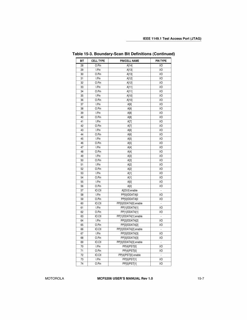
IEEE 1149.1 Test Access Port (JTAG)
MOTOROLA
MCF5206 USERÕS MANUAL Rev 1.0
15-7
28 O.Pin A[14] I/O29 I.Pin A[13] I/O30 O.Pin A[13] I/O31 I.Pin A[12] I/O32 O.Pin A[12] I/O33 I.Pin A[11] I/O34 O.Pin A[11] I/O35 I.Pin A[10] I/O36 O.Pin A[10] I/O37 I.Pin A[9] I/O38 O.Pin A[9] I/O39 I.Pin A[8] I/O40 O.Pin A[8] I/O41 I.Pin A[7] I/O42 O.Pin A[7] I/O43 I.Pin A[6] I/O44 O.Pin A[6] I/O45 I.Pin A[5] I/O46 O.Pin A[5] I/O47 I.Pin A[4] I/O48 O.Pin A[4] I/O49 I.Pin A[3] I/O50 O.Pin A[3] I/O51 I.Pin A[2] I/O52 O.Pin A[2] I/O53 I.Pin A[1] I/O54 O.Pin A[1] I/O55 I.Pin A[0] I/O56 O.Pin A[0] I/O57 IO.Ctl A[23:0] enable -58 I.Pin PP[0]/DDATA[0 I/O59 O.Pin PP[0]/DDATA[0 I/O60 IO.Ctl PP[0]/DDATA[0] enable -61 I.Pin PP[1]/DDATA[1] I/O62 O.Pin PP[1]/DDATA[1] I/O63 IO.Ctl PP[1]/DDATA[1] enable -64 I.Pin PP[2]/DDATA[2] I/O65 O.Pin PP[2]/DDATA[2] I/O66 IO.Ctl PP[2]/DDATA[2] enable -67 I.Pin PP[3]/DDATA[3] I/O68 O.Pin PP[3]/DDATA[3] I/O69 IO.Ctl PP[3]/DDATA[3] enable -70 I.Pin PP[4]/PST[0] I/O71 O.Pin PP[4]/PST[0] I/O72 IO.Ctl PP[4]/PST[0] enable -73 I.Pin PP[5]/PST[1] I/O74 O.Pin PP[5]/PST[1] I/O
Table 15-3. Boundary-Scan Bit Definitions (Continued)
BIT CELL TYPE PIN/CELL NAME PIN TYPE
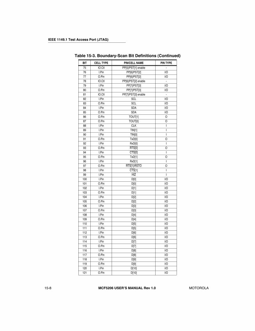
IEEE 1149.1 Test Access Port (JTAG)
15-8
MCF5206 USERÕS MANUAL Rev 1.0
MOTOROLA
75 IO.Ctl PP[5]/PST[1] enable -76 I.Pin PP[6]/PST[2] I/O77 O.Pin PP[6]/PST[2] I/O78 IO.Ctl PP[6]/PST[2] enable -79 I.Pin PP[7]/PST[3] I/O80 O.Pin PP[7]/PST[3] I/O81 IO.Ctl PP[7]/PST[3] enable -82 I.Pin SCL I/O83 O.Pin SCL I/O84 I.Pin SDA I/O85 O.Pin SDA I/O86 O.Pin TOUT[1] O87 O.Pin TOUT[0] O88 I.Pin CLK I89 I.Pin TIN[1] I90 I.Pin TIN[0] I91 O.Pin TxD[0] O92 I.Pin RxD[0] I93 O.Pin RTS[0] O94 I.Pin CTS[0] I95 O.Pin TxD[1] O96 I.Pin RxD[1] I97 O.Pin RTS[1]/RSTO O98 I.Pin CTS[1] I99 I.Pin HIZ I
100 I.Pin D[0] I/O101 O.Pin D[0] I/O102 I.Pin D[1] I/O103 O.Pin D[1] I/O104 I.Pin D[2] I/O105 O.Pin D[2] I/O106 I.Pin D[3] I/O107 O.Pin D[3] I/O108 I.Pin D[4] I/O109 O.Pin D[4] I/O110 I.Pin D[5] I/O111 O.Pin D[5] I/O112 I.Pin D[6] I/O113 O.Pin D[6] I/O114 I.Pin D[7] I/O115 O.Pin D[7] I/O116 I.Pin D[8] I/O117 O.Pin D[8] I/O118 I.Pin D[9] I/O119 O.Pin D[9] I/O120 I.Pin D[10] I/O121 O.Pin D[10] I/O
Table 15-3. Boundary-Scan Bit Definitions (Continued)
BIT CELL TYPE PIN/CELL NAME PIN TYPE

IEEE 1149.1 Test Access Port (JTAG)
MOTOROLA
MCF5206 USERÕS MANUAL Rev 1.0
15-9
122 I.Pin D[11] I/O123 O.Pin D[11] I/O124 I.Pin D[12] I/O125 O.Pin D[12] I/O126 I.Pin D[13] I/O127 O.Pin D[13] I/O128 I.Pin D[14] I/O129 O.Pin D[14] I/O130 I.Pin D[15] I/O131 O.Pin D[15] I/O132 I.Pin D[16] I/O133 O.Pin D[16] I/O134 I.Pin D[17] I/O135 O.Pin D[17] I/O136 I.Pin D[18] I/O137 O.Pin D[18] I/O138 I.Pin D[19] I/O139 O.Pin D[19] I/O140 I.Pin D[20] I/O141 O.Pin D[20] I/O142 I.Pin D[21] I/O143 O.Pin D[21] I/O144 I.Pin D[22] I/O145 O.Pin D[22] I/O146 I.Pin D[23] I/O147 O.Pin D[23] I/O148 I.Pin D[24] I/O149 O.Pin D[24] I/O150 I.Pin D[25] I/O151 O.Pin D[25] I/O152 I.Pin D[26] I/O153 O.Pin D[26] I/O154 I.Pin D[27] I/O155 O.Pin D[27] I/O156 I.Pin D[28] I/O157 O.Pin D[28] I/O158 I.Pin D[29] I/O159 O.Pin D[29] I/O160 I.Pin D[30] I/O161 O.Pin D[30] I/O162 I.Pin D[31] I/O163 O.Pin D[31] I/O164 IO.Ctl D[31:0] enable -165 O.Pin DRAMW O166 O.Pin CAS[3] O167 O.Pin CAS[2] O168 O.Pin CAS[1] O
Table 15-3. Boundary-Scan Bit Definitions (Continued)
BIT CELL TYPE PIN/CELL NAME PIN TYPE
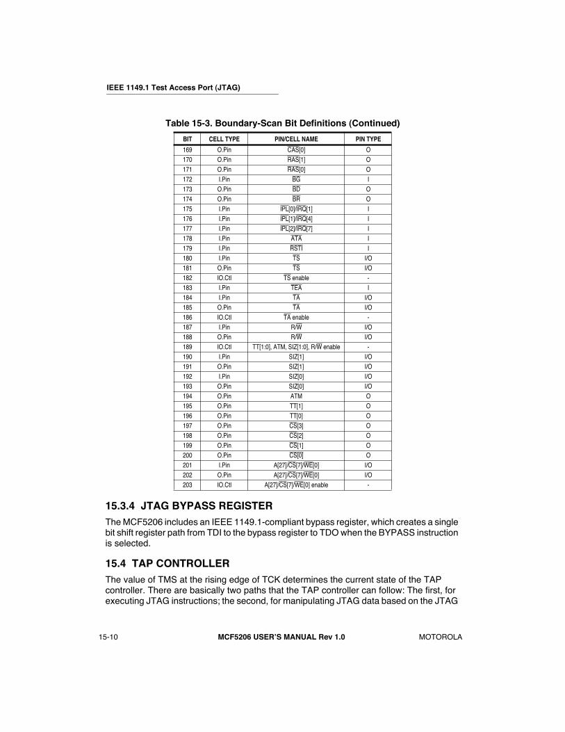
IEEE 1149.1 Test Access Port (JTAG)
15-10
MCF5206 USERÕS MANUAL Rev 1.0
MOTOROLA
15.3.4 JTAG BYPASS REGISTER
The MCF5206 includes an IEEE 1149.1-compliant bypass register, which creates a single bit shift register path from TDI to the bypass register to TDO when the BYPASS instruction is selected.
15.4 TAP CONTROLLER
The value of TMS at the rising edge of TCK determines the current state of the TAP controller. There are basically two paths that the TAP controller can follow: The first, for executing JTAG instructions; the second, for manipulating JTAG data based on the JTAG
169 O.Pin CAS[0] O170 O.Pin RAS[1] O171 O.Pin RAS[0] O172 I.Pin BG I173 O.Pin BD O174 O.Pin BR O175 I.Pin IPL[0]/IRQ[1] I176 I.Pin IPL[1]/IRQ[4] I177 I.Pin IPL[2]/IRQ[7] I178 I.Pin ATA I179 I.Pin RSTI I180 I.Pin TS I/O181 O.Pin TS I/O182 IO.Ctl TS enable -183 I.Pin TEA I184 I.Pin TA I/O185 O.Pin TA I/O186 IO.Ctl TA enable -187 I.Pin R/W I/O188 O.Pin R/W I/O189 IO.Ctl TT[1:0], ATM, SIZ[1:0], R/W enable -190 I.Pin SIZ[1] I/O191 O.Pin SIZ[1] I/O192 I.Pin SIZ[0] I/O193 O.Pin SIZ[0] I/O194 O.Pin ATM O195 O.Pin TT[1] O196 O.Pin TT[0] O197 O.Pin CS[3] O198 O.Pin CS[2] O199 O.Pin CS[1] O200 O.Pin CS[0] O201 I.Pin A[27]/CS[7]/WE[0] I/O202 O.Pin A[27]/CS[7]/WE[0] I/O203 IO.Ctl A[27]/CS[7]/WE[0] enable -
Table 15-3. Boundary-Scan Bit Definitions (Continued)
BIT CELL TYPE PIN/CELL NAME PIN TYPE
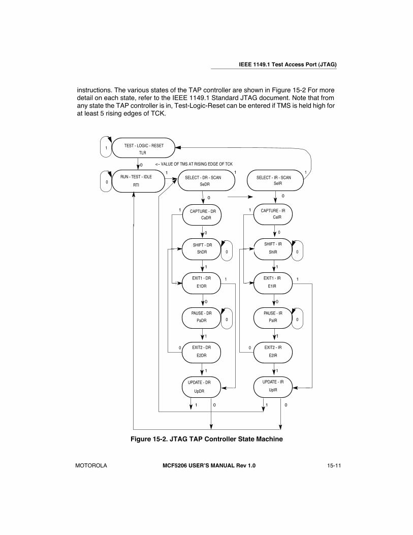
IEEE 1149.1 Test Access Port (JTAG)
MOTOROLA
MCF5206 USERÕS MANUAL Rev 1.0
15-11
instructions. The various states of the TAP controller are shown in Figure 15-2 For more detail on each state, refer to the IEEE 1149.1 Standard JTAG document. Note that from any state the TAP controller is in, Test-Logic-Reset can be entered if TMS is held high for at least 5 rising edges of TCK.
Figure 15-2. JTAG TAP Controller State Machine
TEST - LOGIC - RESET
TLR
RUN - TEST - IDLE
RTI
SELECT - DR - SCAN
SeDR
CAPTURE - IR
UPDATE - IR
EXIT2 - IR
PAUSE - IR
EXIT1 - IR
SHIFT - IR
CAPTURE - DR
UPDATE - DR
EXIT2 - DR
PAUSE - DR
EXIT1 - DR
SHIFT - DR
0
0
0
1
0
1
1
0
0
0
1
0
1
1
0
1 11
1 1
0
0
0
0
1 1
1 1
0 0
0
1
CaDR
ShDR
E1DR
PaDR
E2DR
UpDR
CaIR
ShIR
E1IR
PaIR
E2IR
UpIR
<-- VALUE OF TMS AT RISING EDGE OF TCK
SELECT - IR - SCANSeIR
1
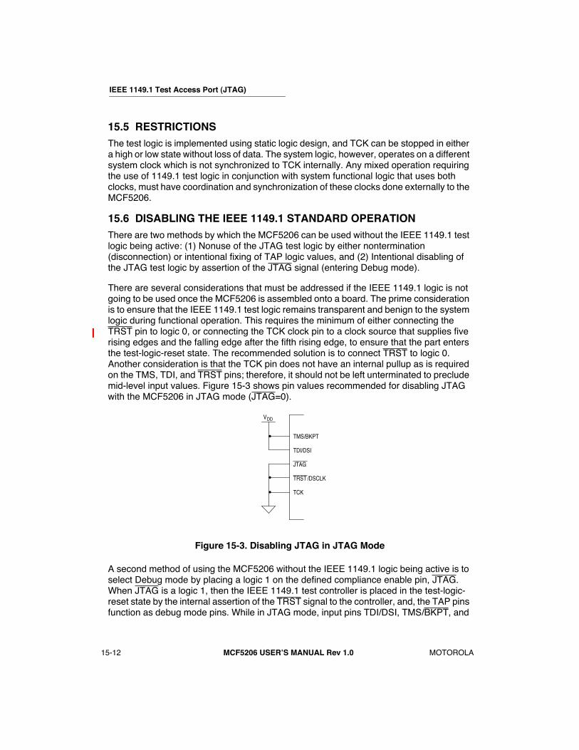
IEEE 1149.1 Test Access Port (JTAG)
15-12
MCF5206 USERÕS MANUAL Rev 1.0
MOTOROLA
15.5 RESTRICTIONS
The test logic is implemented using static logic design, and TCK can be stopped in either a high or low state without loss of data. The system logic, however, operates on a different system clock which is not synchronized to TCK internally. Any mixed operation requiring the use of 1149.1 test logic in conjunction with system functional logic that uses both clocks, must have coordination and synchronization of these clocks done externally to the MCF5206.
15.6 DISABLING THE IEEE 1149.1 STANDARD OPERATION
There are two methods by which the MCF5206 can be used without the IEEE 1149.1 test logic being active: (1) Nonuse of the JTAG test logic by either nontermination (disconnection) or intentional fixing of TAP logic values, and (2) Intentional disabling of the JTAG test logic by assertion of the JTAG signal (entering Debug mode).
There are several considerations that must be addressed if the IEEE 1149.1 logic is not going to be used once the MCF5206 is assembled onto a board. The prime consideration is to ensure that the IEEE 1149.1 test logic remains transparent and benign to the system logic during functional operation. This requires the minimum of either connecting the TRST pin to logic 0, or connecting the TCK clock pin to a clock source that supplies five rising edges and the falling edge after the fifth rising edge, to ensure that the part enters the test-logic-reset state. The recommended solution is to connect TRST to logic 0. Another consideration is that the TCK pin does not have an internal pullup as is required on the TMS, TDI, and TRST pins; therefore, it should not be left unterminated to preclude mid-level input values. Figure 15-3 shows pin values recommended for disabling JTAG with the MCF5206 in JTAG mode (JTAG=0).
Figure 15-3. Disabling JTAG in JTAG Mode
A second method of using the MCF5206 without the IEEE 1149.1 logic being active is to select Debug mode by placing a logic 1 on the defined compliance enable pin, JTAG. When JTAG is a logic 1, then the IEEE 1149.1 test controller is placed in the test-logic-reset state by the internal assertion of the TRST signal to the controller, and, the TAP pins function as debug mode pins. While in JTAG mode, input pins TDI/DSI, TMS/BKPT, and
JTAG
TDI/DSI
TCK
VDD
TRST /DSCLK
TMS/BKPT¥
¥¥

IEEE 1149.1 Test Access Port (JTAG)
MOTOROLA
MCF5206 USERÕS MANUAL Rev 1.0
15-13
TRST/DSCLK have internal pullups enabled. Figure 15-4 shows pin values recommended for disabling JTAG with the MCF5206 in debug mode.
Figure 15-4. Disabling JTAG in Debug Mode
15.7 MOTOROLA MCF5206 BSDL DESCRIPTION
The MCF5206 BSDL description is available on the World Wide Web at http://www.mot.com/coldfire
15.8 OBTAINING THE IEEE 1149.1 STANDARD
The IEEE 1149 Standard JTAG specification is available directly from IEEE:
IEEE Standards Department445 Hoes LaneP.O. Box 1331Piscataway, NJ 08855-1331USA
http://stdsbbs.ieee.org/
Fax: 908-981-9667Information: 908-981-0060 or 1-800-678-4333
JTAG
TDI /DSI
TCK
DEBUG INTERFACE
VDD
TRST /DSCLK
TMS/BKPT
MOTOROLA
MCF5206 USERÕS MANUAL Rev 1.1
16-1
SECTION 16ELECTRICAL CHARACTERISTICS
16.1 MAXIMUM RATINGS
16.1.1 Supply, Input Voltage and Storage Temperature
The ratings in the above table deÞne maximum conditions under which theMCF5206 device may be subjected without being damaged. However, the devicecannot operate normally while being exposed to these electrical extremes.
This device contains circuitry that protects against damage from high staticvoltages or electrical Þelds; however, you should take normal precautions to avoidapplication of any voltages higher than maximum-rated voltages to this high-impedance circuit. Operational reliability improves when unused inputs are tied toan appropriate logic voltage level (e.g., either GND or V
DD
).
16.1.2 Operating Temperature
a
This published maximum operating ambient temperature should be used only as a system design guideline. All device operating parameters are guaranteed only when the junction temperature lies within the speciÞed range.
NOTE
At press time power dissipation Þgures were not available. Refer to the World Wide Web site at http://www.mot.com/ColdFire for the latest accurate power dissipation
information for the MCF5206 processor.
RATING SYMBOL VALUE UNIT
Supply voltage V
DD
-0.3 to +7.0 V
Input voltage V
in
-0.5 to V
DD
+ 0.5V
V
Storage temperature range T
stg
-55 to 150
o
C
CHARACTERISTIC SYMBOL VALUE UNIT
Maximum operating junction temperature T
J
TBD
o
C
Maximum operating ambient temperature T
Amax
70
a
o
C
Minimum operating ambient temperature T
Amin
0
o
C
REVISION NO.: 1.1REVISION DATE: 6/17/98, 8/28/98PAGES AFFECTED: SEE RED CHANGE BARS

Electrical Characteristics (REV. 1.0 6/17/98)(Rev 1.1 8/28/98)
16-2
MCF5206 USERÕS MANUAL Rev 1.1
MOTOROLA
16.1.3 Thermal Resistance
16.1.4 Output Loading
16.2
DC ELECTRICAL SPECIFICATIONS
* This speciÞcation periodically sampled but not 100% tested.
CHARACTERISTIC VALUE RATING
Thermal resistance, junction to ambientThermal resistance, junction to top reference
q
ja
Y
jt
383
o
C/W
o
C/W
b
q
ja
and Y
jt
parameters are simulated in accordance with EIA/JESD Standard 51-2 for natural convection. Motorola recommends the use of q
ja
and power dissipation specifications in the system design to prevent device junction temperatures from exceeding the rated specification. System designers should be aware that device junction temperatures can be significantly influenced by the board layout and surrounding devices. Conformance to the device junction temperature specification can be verified by physical measurement in the customerÕs system using the Y
jt
parameter, the device power dissipation, and the method described in EIA/JESD Standard 51-2.
CHARACTERISTIC SYMBOL MAXIMUM UNIT
Load Capacitance (All signals) C
L
50 pF
CHARACTERISTIC SYMBOL MIN MAX UNIT
Operation voltage range
V
DD
4.75 5.25 V
Input high voltage
V
IH
2 V
DD
V
Input low voltage
V
IL
GND 0.8 V
Input signal undershoot
Ñ Ñ 0.8 V
Input signal overshoot
Ñ Ñ 0.8 V
Input leakage current @ GND, V
DD
CLK, A[27:0], D[31:0], TS, SIZ[1:0], R/W, TA, ATA, TEA, IPL[2]/IRQ[7],IPL[1]/IRQ[4], IPL[0]/IRQ[1], BG, RxD[2:1], CTS[2:1], TIN[1:0],PP[7:0]/PST[3:0]:DDATA[3:0], RSTI, TCK, HIZ, JTAG
I
in
Ñ 20
m
A
HI-Z (three-state) leakage current @GND, V
DD
A[27:0], D[31:0], TS, TT[1:0], ATM, SIZ[1:0], R/W, TA, TDO/DSO
I
TSI
Ñ 20
m
A
Signal Low Input Current, V
IL
= 0.8VTMS/BKPT, TDI/DSI, TRST/DSCLK
I
IL
TBD TBD mA
Signal High Input Current, V
IH
= 2.0VTMS/BKPT, TDI/DSI, TRST/DSCLK
I
IH
TBD TBD mA
Output high voltage, I
OH
= 8 mA ( All signals except RAS[1:0], CAS[3:0], DRAMW), I
OH
=16mA (RAS[1:0], CAS[3:0], DRAMW)
V
OH
2.4 Ñ V
Output low voltage , I
OL
= 8 mA ( All signals except RAS[1:0], CAS[3:0], DRAMW), I
OL
= 16mA (RAS[1:0], CAS[3:0], DRAMW)
V
OL
Ñ 0.5 V
Pin capacitance*
C
in
Ñ 10 pF
SYMBOL
b

(Rev 1.1 8/28/98)(REV. 1.0 6/17/98) Electrical Characteristics
MOTOROLA
MCF5206 USERÕS MANUAL Rev 1.1
16-3
16.3 AC ELECTRICAL SPECIFICATIONS
16.3.1 Clock Input Timing Specifications
1
CLK may be stopped to conserve power.
2
SpeciÞcation values are not tested.
3
SpeciÞcation values listed are for maximum frequency of operation.
16.3.2 Clock Input Timing Diagram
Clock Input Timing
NAME CHARACTERISTIC
16.67 MHz 25 MHz
33 .33MHz
UNIT
MIN MAX MIN MAX MIN MAX
Frequency of Operation
1
0 16.67 0 25.00 0 33.33 MHz
C1 CLK cycle time 60 Ñ 40 Ñ 30 Ñ ns
C2
2
CLK rise time (from
V
l
= 0.5V to V
h
= 2.4V)
Ñ 5 Ñ 5 Ñ 5 ns
C3
2
CLK fall time
(
from
V
h
= 0.5V to V
l
= 2.4V)
Ñ 5 Ñ 5 Ñ 5 ns
C4 CLK duty cycle (measured at 1.5 V) 40 60 40 60 40 60 %
C4a
3
CLK pulse width high (measured at 1.5 V) 24 36 16 24 12 18 ns
C4b
3
CLK pulse width low (measured at 1.5 V) 24 36 16 24 12 18 ns
CLK
C1
C4a C4b
C3C2Vh
Vl

Electrical Characteristics (REV. 1.0 6/17/98)(Rev 1.1 8/28/98)
16-4
MCF5206 USERÕS MANUAL Rev 1.1
MOTOROLA
16.3.3 Processor Bus Input Timing Specifications
16.3.4 Input Timing Waveform Diagram
Input Timing Waveform Requirements
NAME CHARACTERISTIC16.67 MHz 25 MHz 33.33 MHz
UNITMIN MAX MIN MAX MIN MAX
CONTROL INPUTS
B1a TS Valid to CLK (Setup) 15 Ñ 10 Ñ 7 Ñ nsB1b TA, Valid to CLK (Setup) 15 Ñ 10 Ñ 8 Ñ nsB1c ATA Valid to CLK (Setup) 3 Ñ 3 Ñ 2 Ñ nsB1d TEA Valid to CLK (Setup) 15 Ñ 11 Ñ 10 Ñ nsB1e BG Valid to CLK (Setup) 15 Ñ 10 Ñ 10 Ñ nsB1f IPL[2:0]/IRQ[7,4,1] Valid to CLK (Setup) 3 Ñ 3 Ñ 2 Ñ nsB1g RSTI Valid to CLK (Setup) 3 Ñ 3 Ñ 2 Ñ nsB1h DSCLK to CLK (Setup) 15 Ñ 13 Ñ 11 Ñ nsB1i BKPT, DSI Valid to CLK (Setup) 15 Ñ 10 Ñ 7 Ñ ns
B2a CLK to Synchronous Control Input(TS, TA, TEA, BG, DSI, DSCLK) Invalid (Hold) 3 Ñ 3 Ñ 2 Ñ ns
B2b CLK to Asynchronous Control Input(ATA, IPL[2:0]/IRQ[7,4,1], RSTI, BKPT) Invalid (Hold) 3 Ñ 3 Ñ 3 Ñ ns
B2c CLK to Mode Selects Invalid (RSTI Asserted) 3 Ñ 3 Ñ 2 Ñ ns
ADDRESS AND ATTRIBUTE INPUTS
B3 Address and Attribute Input(A[27:0], SIZ[1:0], R/W) Valid to CLK (Setup) 15 Ñ 10 Ñ 7 Ñ ns
B4 CLK to Address and Attribute Input(A[27:0], SIZ[1:0], R/W) Invalid (Hold) 3 Ñ 3 Ñ 2 Ñ ns
DATA INPUTS
B5 Data Input (D[31:0]) Valid to CLK (Setup) 10 Ñ 6 Ñ 3 Ñ nsB6 CLK to Data Input (D[31:0]) Invalid (Hold) 3 Ñ 3 Ñ 3 Ñ ns
INVALID INVALID
CLKTSETUP
THOLD
INPUT SETUP AND HOLD
1.5V
trise £ 1.5nsVh = VIH
Vl = VIL
1.5V1.5V VALID
tfall £ 1.5nsVh = VIH
Vl = VIL
INPUT RISE TIME
INPUT FALL TIME
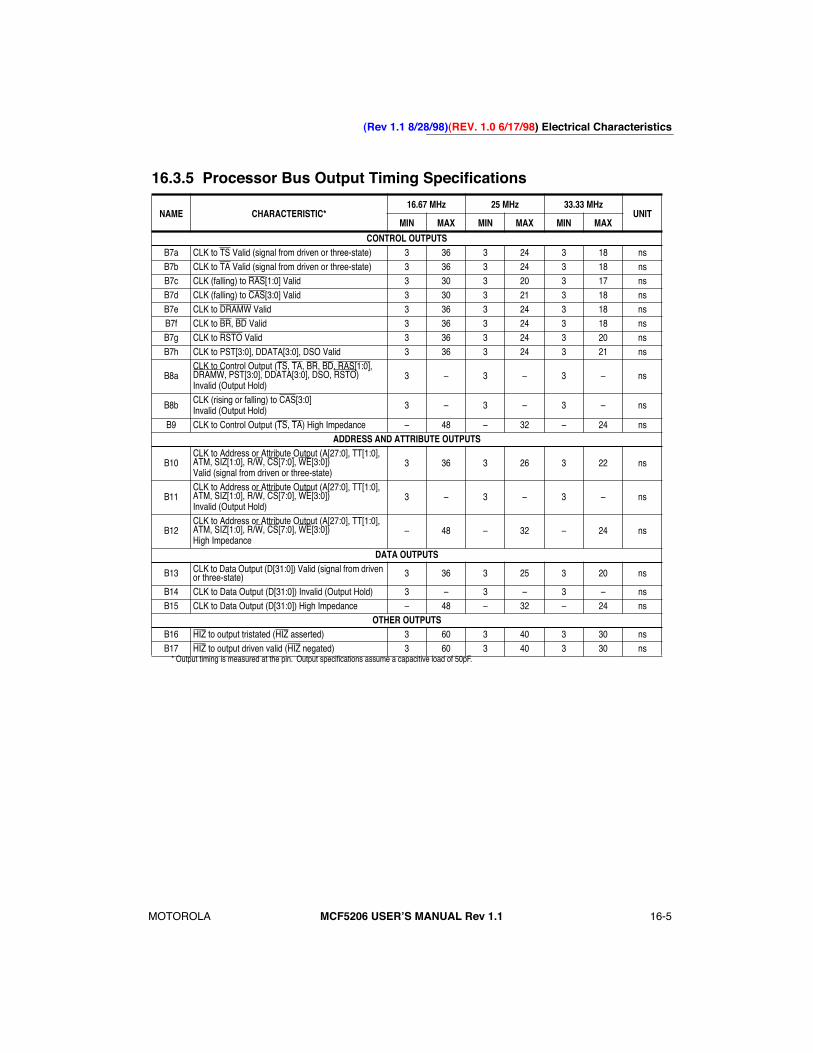
(Rev 1.1 8/28/98)(REV. 1.0 6/17/98) Electrical Characteristics
MOTOROLA
MCF5206 USERÕS MANUAL Rev 1.1
16-5
16.3.5 Processor Bus Output Timing Specifications
* Output timing is measured at the pin. Output speciÞcations assume a capacitive load of 50pF.
NAME CHARACTERISTIC*16.67 MHz 25 MHz 33.33 MHz
UNITMIN MAX MIN MAX MIN MAX
CONTROL OUTPUTS
B7a CLK to TS Valid (signal from driven or three-state) 3 36 3 24 3 18 nsB7b CLK to TA Valid (signal from driven or three-state) 3 36 3 24 3 18 nsB7c CLK (falling) to RAS[1:0] Valid 3 30 3 20 3 17 nsB7d CLK (falling) to CAS[3:0] Valid 3 30 3 21 3 18 nsB7e CLK to DRAMW Valid 3 36 3 24 3 18 nsB7f CLK to BR, BD Valid 3 36 3 24 3 18 nsB7g CLK to RSTO Valid 3 36 3 24 3 20 nsB7h CLK to PST[3:0], DDATA[3:0], DSO Valid 3 36 3 24 3 21 ns
B8aCLK to Control Output (TS, TA, BR, BD, RAS[1:0], DRAMW, PST[3:0], DDATA[3:0], DSO, RSTO)Invalid (Output Hold)
3 Ð 3 Ð 3 Ð ns
B8b CLK (rising or falling) to CAS[3:0]Invalid (Output Hold) 3 Ð 3 Ð 3 Ð ns
B9 CLK to Control Output (TS, TA) High Impedance Ð 48 Ð 32 Ð 24 ns
ADDRESS AND ATTRIBUTE OUTPUTS
B10CLK to Address or Attribute Output (A[27:0], TT[1:0], ATM, SIZ[1:0], R/W, CS[7:0], WE[3:0])Valid (signal from driven or three-state)
3 36 3 26 3 22 ns
B11CLK to Address or Attribute Output (A[27:0], TT[1:0], ATM, SIZ[1:0], R/W, CS[7:0], WE[3:0])Invalid (Output Hold)
3 Ð 3 Ð 3 Ð ns
B12CLK to Address or Attribute Output (A[27:0], TT[1:0], ATM, SIZ[1:0], R/W, CS[7:0], WE[3:0])High Impedance
Ð 48 Ð 32 Ð 24 ns
DATA OUTPUTS
B13 CLK to Data Output (D[31:0]) Valid (signal from driven or three-state) 3 36 3 25 3 20 ns
B14 CLK to Data Output (D[31:0]) Invalid (Output Hold) 3 Ð 3 Ð 3 Ð nsB15 CLK to Data Output (D[31:0]) High Impedance Ð 48 Ð 32 Ð 24 ns
OTHER OUTPUTS
B16 HIZ to output tristated (HIZ asserted) 3 60 3 40 3 30 nsB17 HIZ to output driven valid (HIZ negated) 3 60 3 40 3 30 ns

Electrical Characteristics (REV. 1.0 6/17/98)(Rev 1.1 8/28/98)
16-6
MCF5206 USERÕS MANUAL Rev 1.1
MOTOROLA
16.3.6 Output Timing Waveform Diagram
Output Timing Waveform
INVALID
INVALID
CLK (POSITIVE)
THOLD
OUTPUT HOLD 1.5V
1.5V
VALID
1.5V
TVALID
OUTPUT VALID 1.5V
INVALID
VALID
CLK (NEGATIVE)
THOLD
OUTPUT 1.5VVALID
TVALID
OUTPUT 1.5V
INVALID
VALID
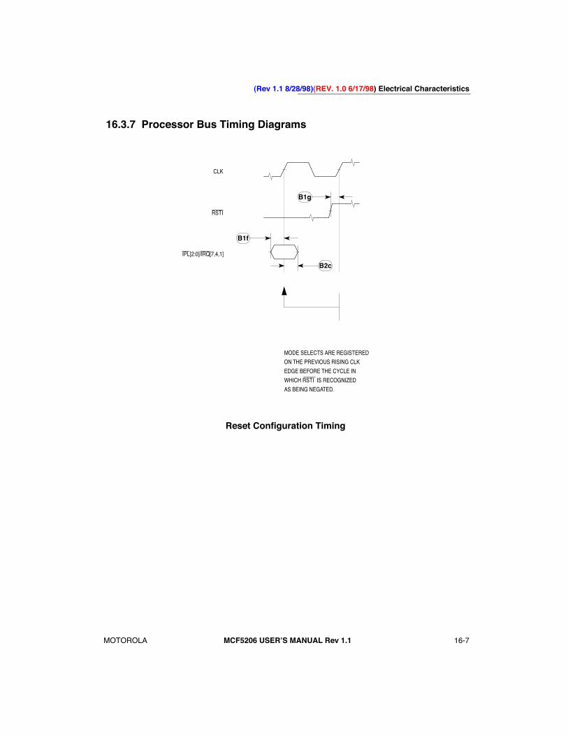
(Rev 1.1 8/28/98)(REV. 1.0 6/17/98) Electrical Characteristics
MOTOROLA
MCF5206 USERÕS MANUAL Rev 1.1
16-7
16.3.7 Processor Bus Timing Diagrams
Reset Configuration Timing
RSTI
CLK
IPL[2:0]/IRQ[7,4,1]
B1g
B2c
MODE SELECTS ARE REGISTERED
ON THE PREVIOUS RISING CLK
B1f
EDGE BEFORE THE CYCLE IN
WHICH RSTI IS RECOGNIZED
AS BEING NEGATED.
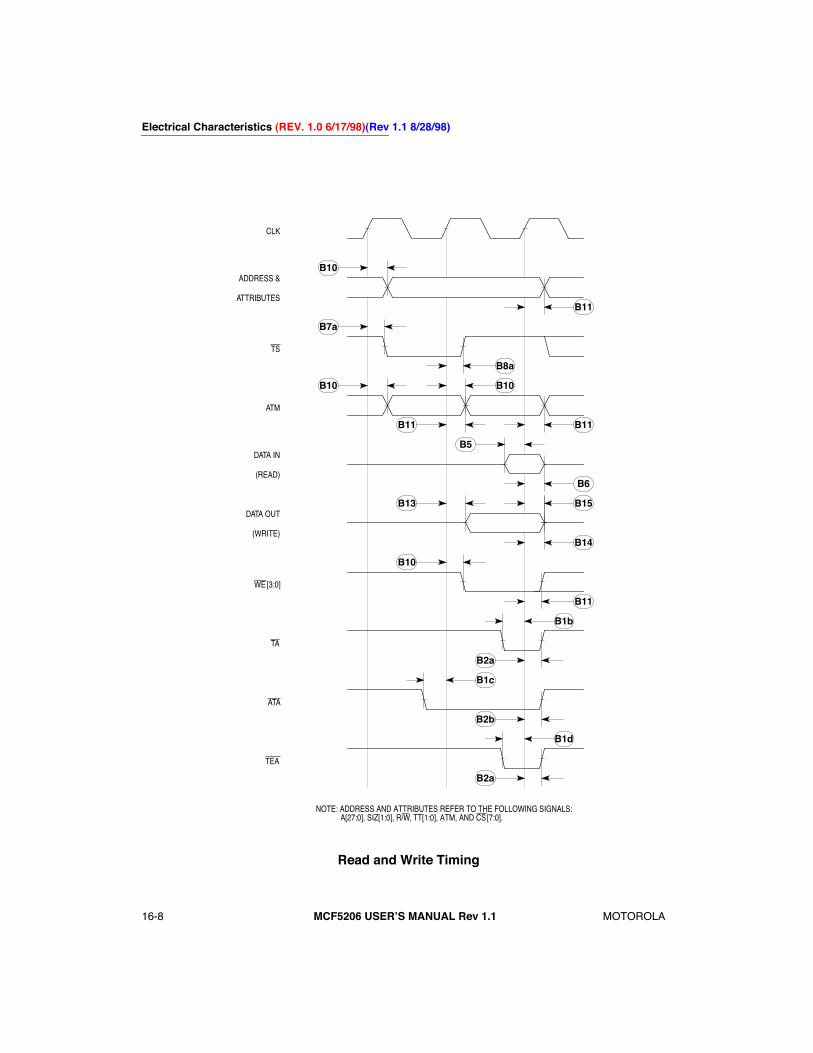
Electrical Characteristics (REV. 1.0 6/17/98)(Rev 1.1 8/28/98)
16-8
MCF5206 USERÕS MANUAL Rev 1.1
MOTOROLA
Read and Write Timing
NOTE: ADDRESS AND ATTRIBUTES REFER TO THE FOLLOWING SIGNALS:A[27:0], SIZ[1:0], R/W, TT[1:0], ATM, AND CS[7:0].
CLK
B8a
B7a
ADDRESS &
ATTRIBUTES
B5DATA IN
(READ)
DATA OUT
(WRITE)
B13 B15
TS
ATM
WE [3:0]
B2a
B2b
ATA
B6
B14
B1c
B1b
B11
B10
B11
B10
B11
B10
B11
B10
TA
B2a
B1d
TEA
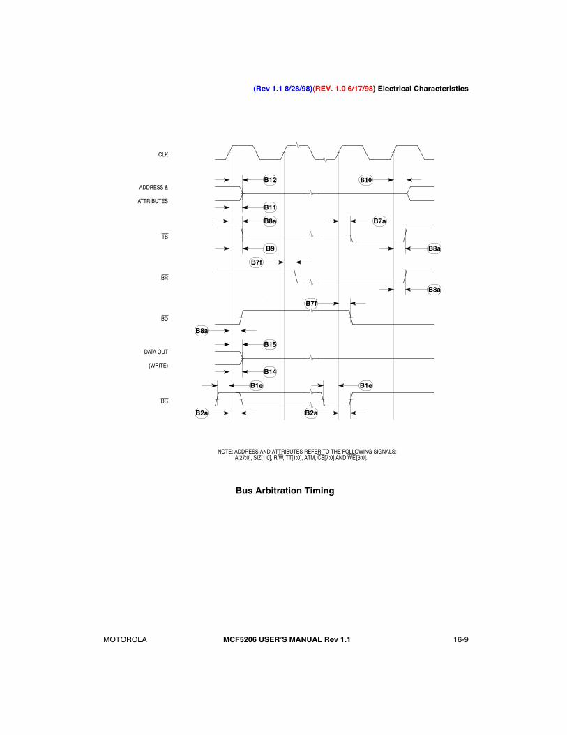
(Rev 1.1 8/28/98)(REV. 1.0 6/17/98) Electrical Characteristics
MOTOROLA
MCF5206 USERÕS MANUAL Rev 1.1
16-9
Bus Arbitration Timing
NOTE: ADDRESS AND ATTRIBUTES REFER TO THE FOLLOWING SIGNALS:A[27:0], SIZ[1:0], R/W, TT[1:0], ATM, CS[7:0] AND WE [3:0].
ADDRESS &
ATTRIBUTES
TS
BG
B11
B10B12
B7aB8a
B9
B14
B15DATA OUT
(WRITE)
B8a
BD
B8a
B2a
B1eB1e
B2a
CLK
B7f
B7f
B8a
BR
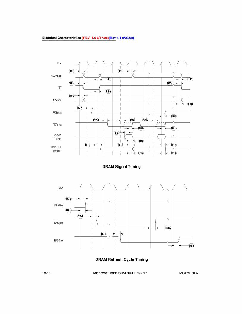
Electrical Characteristics (REV. 1.0 6/17/98)(Rev 1.1 8/28/98)
16-10
MCF5206 USERÕS MANUAL Rev 1.1
MOTOROLA
DRAM Signal Timing
DRAM Refresh Cycle Timing
CLK
B8a
B7a
DATA IN
(READ)
DATA OUT
(WRITE)
B13
TS
DRAMW
B14
B10
B7c
B7d
RAS [1:0]
CAS [3:0]
ADDRESS
B8b
B11 B11
B5
B6B15
B14
B13
B8b
B10
B8a
B8b
B8b
B7e
B8a
B7a
CLK
B7d
B7c
CAS [3:0]
RAS [1:0]
B8b
B8a
DRAMW
B8a
B7e

(Rev 1.1 8/28/98)(REV. 1.0 6/17/98) Electrical Characteristics
MOTOROLA MCF5206 USERÕS MANUAL Rev 1.1 16-11
DRAM Control By Alternate Master Timing
CLK
DRAMW
B7c
B7d
RAS [1:0]
CAS [3:0]
B8bB8a
B8b
ALT. MASTER
TS INB2a
B1a
B3
B4
B10
ADDRESSB11 B12
TA
B2a
B1a
B3
B4
B7b
B8a B9B7b
B7e
ALT. MASTER
ADDRESS,
SIZ[1:0], R/W IN
B7b
B10
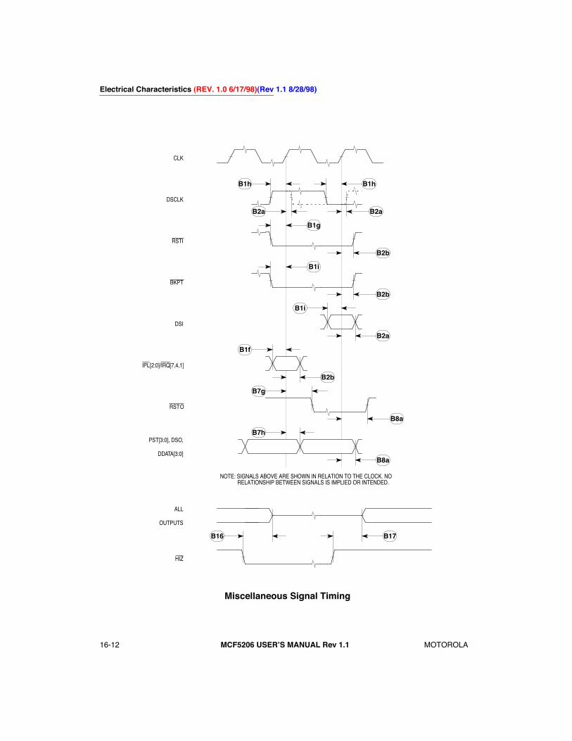
Electrical Characteristics (REV. 1.0 6/17/98)(Rev 1.1 8/28/98)
16-12 MCF5206 USERÕS MANUAL Rev 1.1 MOTOROLA
Miscellaneous Signal Timing
RSTI
B2b
CLK
B1f
B2b
B1g
HIZ
ALL
OUTPUTS
B16 B17
IPL[2:0]/IRQ[7,4,1]
BKPT
B2b
B1i
DSI
B1i
B2a
B7h
B8a
RSTO
B8a
B7g
B1hB1h
DSCLK
PST[3:0], DSO,
DDATA[3:0]
B2aB2a
NOTE: SIGNALS ABOVE ARE SHOWN IN RELATION TO THE CLOCK. NORELATIONSHIP BETWEEN SIGNALS IS IMPLIED OR INTENDED.

(Rev 1.1 8/28/98)(REV. 1.0 6/17/98) Electrical Characteristics
MOTOROLA MCF5206 USERÕS MANUAL Rev 1.1 16-13
16.3.8 Timer Module AC Timing Specifications
16.3.9 Timer Module Timing Diagram
Timer Timing
NAME CHARACTERISTIC16.67 MHz 25 MHz 33.33 MHz
UNITMIN MAX MIN MAX MIN MAX
T1 TIN[1:0] cycle time 3 Ñ 3 Ñ 3 Ñ clkT2 TIN[1:0] Valid to CLK (Setup) 15 Ñ 10 Ñ 7 Ñ nsT3 CLK to TIN[1:0] Invalid (Hold) 3 Ñ 3 Ñ 3 Ñ nsT4 CLK to TOUT[1:0] Valid 3 36 3 24 3 18 nsT5 CLK to TOUT[1:0] Invalid (Output Hold) 3 Ñ 3 Ñ 3 Ñ nsT6 TIN[1:0] pulse width 1 Ñ 1 Ñ 1 Ñ clkT7 TOUT[1:0] pulse width 1 Ñ 1 Ñ 1 Ñ clk
CLK
TOUT[1:0] OUT
TIN[1:0] IN
(CLOCK MODE)
TIN[1:0] IN
(CAPTURE MODE
SYNCHRONIZATION) T2 T3
T1
T6
T7
T2 T3T2
T4 T5

Electrical Characteristics (REV. 1.0 6/17/98)(Rev 1.1 8/28/98)
16-14 MCF5206 USERÕS MANUAL Rev 1.1 MOTOROLA
16.3.10 UART Module AC Timing Specifications
16.3.11 UART Module Timing Diagram
UART Timing
NAME CHARACTERISTIC16.67 MHz 25 MHz 33.33 MHz
UNITMIN MAX MIN MAX MIN MAX
U1 RxD[2:1] Valid to CLK (Setup) 15 Ñ 10 Ñ 7 Ñ nsU2 CLK to RxD[2:1] Invalid (Hold) 3 Ñ 3 Ñ 2 Ñ nsU3 CTS[2:1] Valid to CLK (Setup) 15 Ñ 10 Ñ 7 Ñ nsU4 CLK to CTS[2:1] Invalid (Hold) 3 Ñ 3 Ñ 3 Ñ nsU5 CLK to TxD[2:1] Valid 3 36 3 24 3 18 nsU6 CLK to TxD[2:1] Invalid (Output Hold) 3 Ñ 3 Ñ 3 Ñ nsU7 CLK to RTS[2:1] Valid 3 36 3 24 3 20 nsU8 CLK to RTS[2:1] Invalid (Output Hold) 3 Ñ 3 Ñ 3 Ñ ns
U5
CLK
TXD[2:1] OUT
U6
U1
U2
RXD[2:1] IN
U7
RTS[2:1] OUT
U8
U3
U4
CTS[2:1] IN
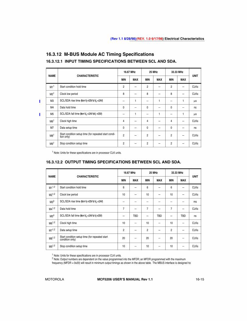
(Rev 1.1 8/28/98)(REV. 1.0 6/17/98) Electrical Characteristics
MOTOROLA MCF5206 USERÕS MANUAL Rev 1.1 16-15
16.3.12 M-BUS Module AC Timing Specifications16.3.12.1 INPUT TIMING SPECIFICATIONS BETWEEN SCL AND SDA.
1 Note: Units for these speciÞcations are in processor CLK units.
16.3.12.2 OUTPUT TIMING SPECIFICATIONS BETWEEN SCL AND SDA.
1 Note: Units for these speciÞcations are in processor CLK units.2 Note: Output numbers are dependent on the value programmed into the MFDR; an MFDR programmed with the maximum frequency (MFDR = 0x20) will result in minimum output timings as shown in the above table. The MBUS interface is designed to
NAME CHARACTERISTIC16.67 MHz 25 MHz 33.33 MHz
UNITMIN MAX MIN MAX MIN MAX
M11 Start condition hold time 2 Ñ 2 Ñ 2 Ñ CLKs
M21 Clock low period 8 Ñ 8 Ñ 8 Ñ CLKs
M3 SCL/SDA rise time (from Vl = 0.5V to Vh = 2.4V) Ñ 1 Ñ 1 Ñ 1 ms
M4 Data hold time 0 Ñ 0 Ñ 0 Ñ ns
M5 SCL/SDA fall time (from Vh = 2.4V toVl = 0.5V) Ñ 1 Ñ 1 Ñ 1 ms
M61 Clock high time 4 Ñ 4 Ñ 4 Ñ CLKs
M7 Data setup time 0 Ñ 0 Ñ 0 Ñ ns
M81 Start condition setup time (for repeated start condi-tion only) 2 Ñ 2 Ñ 2 Ñ CLKs
M91 Stop condition setup time 2 Ñ 2 Ñ 2 Ñ CLKs
NAME CHARACTERISTIC16.67 MHz 25 MHz 33.33 MHz
UNITMIN MAX MIN MAX MIN MAX
M11,2 Start condition hold time 6 Ñ 6 Ñ 6 Ñ CLKs
M21,2 Clock low period 10 Ñ 10 Ñ 10 Ñ CLKs
M33 SCL/SDA rise time (from Vl = 0.5V to Vh = 2.4V) Ñ Ñ Ñ Ñ Ñ Ñ ms
M41,2 Data hold time 7 Ñ 7 Ñ 7 Ñ CLKs
M54 SCL/SDA fall time (from Vh = 2.4V to Vl = 0.5V) Ñ TBD Ñ TBD Ñ TBD ns
M61,2 Clock high time 10 Ñ 10 Ñ 10 Ñ CLKs
M71,2 Data setup time 2 Ñ 2 Ñ 2 Ñ CLKs
M81,2 Start condition setup time (for repeated start condition only) 20 Ñ 20 Ñ 20 Ñ CLKs
M91,2 Stop condition setup time 10 Ñ 10 Ñ 10 Ñ CLKs
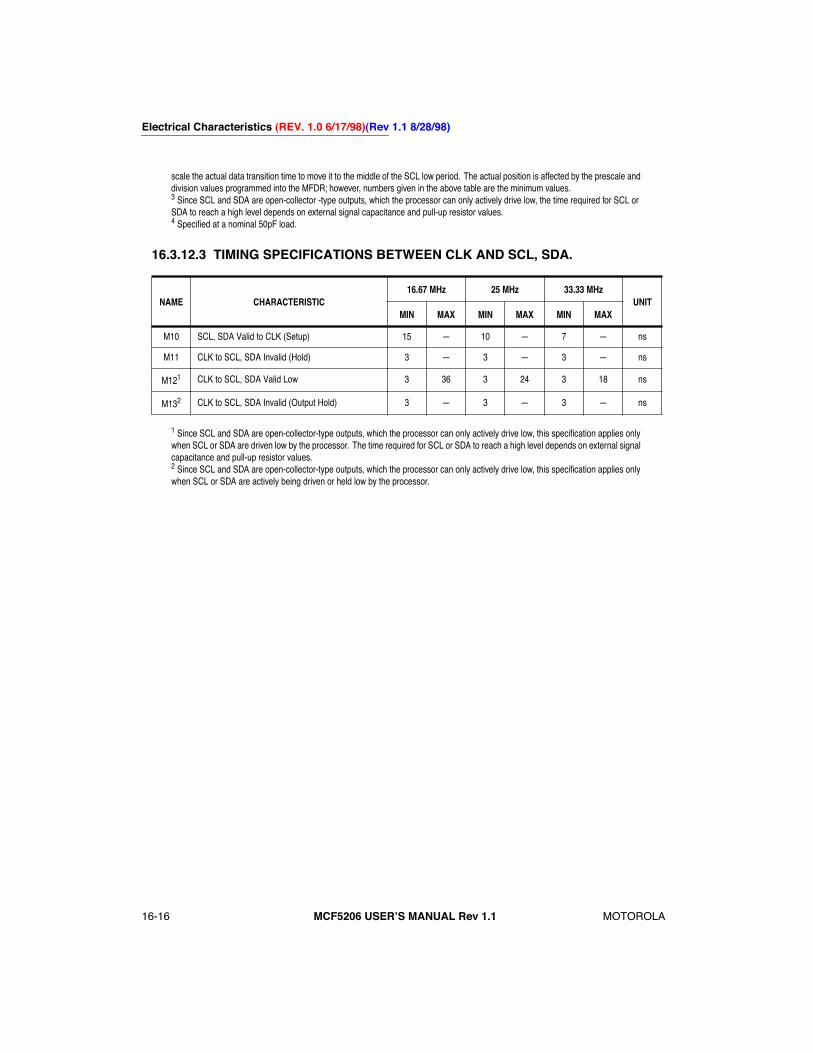
Electrical Characteristics (REV. 1.0 6/17/98)(Rev 1.1 8/28/98)
16-16 MCF5206 USERÕS MANUAL Rev 1.1 MOTOROLA
scale the actual data transition time to move it to the middle of the SCL low period. The actual position is affected by the prescale and division values programmed into the MFDR; however, numbers given in the above table are the minimum values.3 Since SCL and SDA are open-collector -type outputs, which the processor can only actively drive low, the time required for SCL or SDA to reach a high level depends on external signal capacitance and pull-up resistor values.4 SpeciÞed at a nominal 50pF load.
16.3.12.3 TIMING SPECIFICATIONS BETWEEN CLK AND SCL, SDA.
1 Since SCL and SDA are open-collector-type outputs, which the processor can only actively drive low, this speciÞcation applies only when SCL or SDA are driven low by the processor. The time required for SCL or SDA to reach a high level depends on external signal capacitance and pull-up resistor values.2 Since SCL and SDA are open-collector-type outputs, which the processor can only actively drive low, this speciÞcation applies only when SCL or SDA are actively being driven or held low by the processor.
NAME CHARACTERISTIC16.67 MHz 25 MHz 33.33 MHz
UNITMIN MAX MIN MAX MIN MAX
M10 SCL, SDA Valid to CLK (Setup) 15 Ñ 10 Ñ 7 Ñ ns
M11 CLK to SCL, SDA Invalid (Hold) 3 Ñ 3 Ñ 3 Ñ ns
M121 CLK to SCL, SDA Valid Low 3 36 3 24 3 18 ns
M132 CLK to SCL, SDA Invalid (Output Hold) 3 Ñ 3 Ñ 3 Ñ ns

(Rev 1.1 8/28/98)(REV. 1.0 6/17/98) Electrical Characteristics
MOTOROLA MCF5206 USERÕS MANUAL Rev 1.1 16-17
16.3.13 M-Bus Module Timing Diagram
M-Bus Timing
M1
SCL
M3M5 VhVl
M2 M6
SDA
M4 M7 M8 M9
CLK
SCL, SDA OUT
SCL, SDA IN
M12
M13
M10
M11
SCL, SDA OUT

Electrical Characteristics (REV. 1.0 6/17/98)(Rev 1.1 8/28/98)
16-18 MCF5206 USERÕS MANUAL Rev 1.1 MOTOROLA
16.3.14 General-Purpose I/O Port AC Timing Specifications
16.3.15 General-Purpose I/O Port Timing Diagram
General-Purpose I/O Port Timing
NAME CHARACTERISTIC16.67 MHz 25 MHz 33.33 MHz
UNITMIN MAX MIN MAX MIN MAX
P1 PP[7:0]input setup time to CLK (rising) 15 Ñ 10 Ñ 7 Ñ nsP2 PP[7:0] input hold time from CLK (rising) 3 Ñ 3 Ñ 3 Ñ nsP3 CLK to PP[7:0] Output Valid 3 36 3 24 3 21 nsP4 CLK to PP[7:0] Output Invalid (Output Hold) 3 Ñ 3 Ñ 3 Ñ ns
P3
CLK
PP[7:0] OUT
P4
P1
P2
PP[7:0] IN
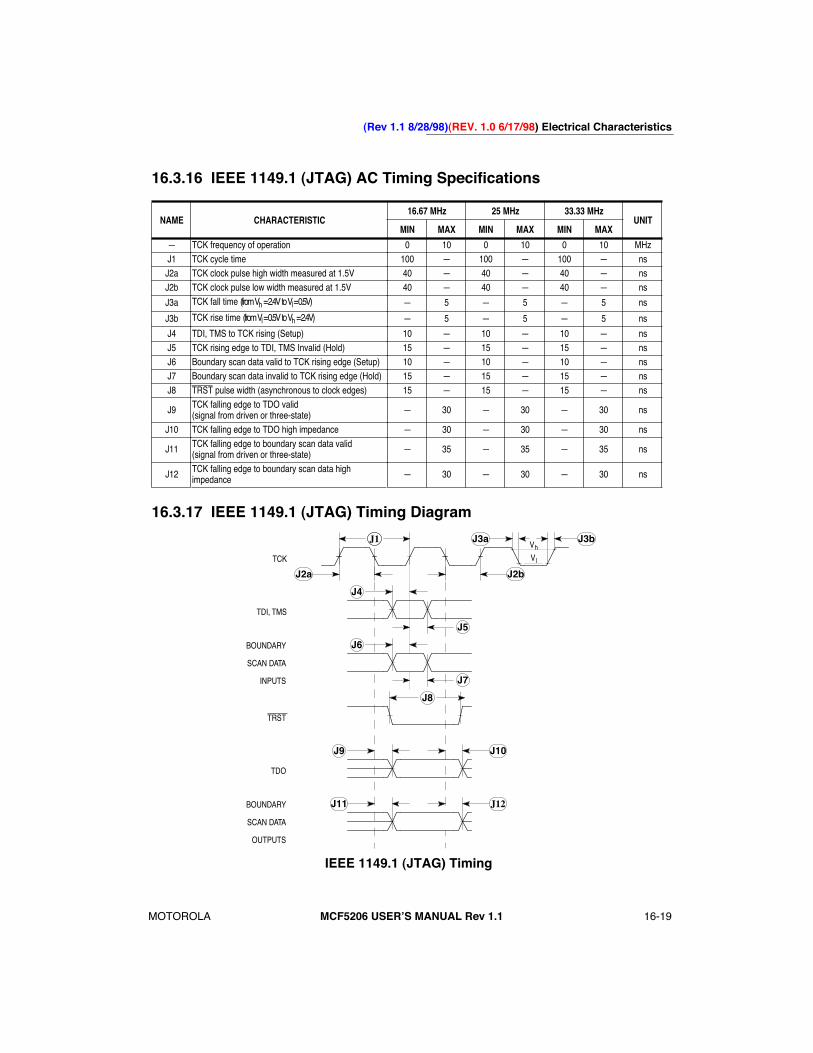
(Rev 1.1 8/28/98)(REV. 1.0 6/17/98) Electrical Characteristics
MOTOROLA MCF5206 USERÕS MANUAL Rev 1.1 16-19
16.3.16 IEEE 1149.1 (JTAG) AC Timing Specifications
16.3.17 IEEE 1149.1 (JTAG) Timing Diagram
IEEE 1149.1 (JTAG) Timing
NAME CHARACTERISTIC16.67 MHz 25 MHz 33.33 MHz
UNITMIN MAX MIN MAX MIN MAX
Ñ TCK frequency of operation 0 10 0 10 0 10 MHzJ1 TCK cycle time 100 Ñ 100 Ñ 100 Ñ nsJ2a TCK clock pulse high width measured at 1.5V 40 Ñ 40 Ñ 40 Ñ nsJ2b TCK clock pulse low width measured at 1.5V 40 Ñ 40 Ñ 40 Ñ ns
J3a TCK fall time (from Vh = 2.4V to Vl = 0.5V) Ñ 5 Ñ 5 Ñ 5 ns
J3b TCK rise time (from Vl = 0.5V to Vh = 2.4V) Ñ 5 Ñ 5 Ñ 5 ns
J4 TDI, TMS to TCK rising (Setup) 10 Ñ 10 Ñ 10 Ñ nsJ5 TCK rising edge to TDI, TMS Invalid (Hold) 15 Ñ 15 Ñ 15 Ñ nsJ6 Boundary scan data valid to TCK rising edge (Setup) 10 Ñ 10 Ñ 10 Ñ nsJ7 Boundary scan data invalid to TCK rising edge (Hold) 15 Ñ 15 Ñ 15 Ñ nsJ8 TRST pulse width (asynchronous to clock edges) 15 Ñ 15 Ñ 15 Ñ ns
J9 TCK falling edge to TDO valid(signal from driven or three-state) Ñ 30 Ñ 30 Ñ 30 ns
J10 TCK falling edge to TDO high impedance Ñ 30 Ñ 30 Ñ 30 ns
J11 TCK falling edge to boundary scan data valid(signal from driven or three-state) Ñ 35 Ñ 35 Ñ 35 ns
J12 TCK falling edge to boundary scan data highimpedance Ñ 30 Ñ 30 Ñ 30 ns
TCK
J1 J3bJ3aVh
Vl
J2a J2b
J4
J5
J6
J7
BOUNDARY
SCAN DATA
INPUTS
J9 J10
TRST
TDO
BOUNDARY
SCAN DATA
OUTPUTS
J8
J11 J12
TDI, TMS

MOTOROLA
MCF5206 USERÕS MANUAL Rev 1.0
17-1
SECTION 17MECHANICAL DATA
ÇÇÇÇÇÇÇÇÇÇÇÇÇÇÇ
ÉÉÉÉÉÉ
DETAIL C
±H±
±B±±A±
±D±
LY
DETAIL A
B VL
Z
A
S
!��������������� � !�
��������������
!��������������� � !�
!���
������������
�!
�
!���
������������
�!
�
DETAIL A
G
P
±A±, ±B±, ±D±
BB
±H±
±C±
EC
M
U
WK
X
Q
R
T
H�����������
�
�
�
������������
!��������������� � !�
D
N
F
J
BASEMETAL
SECTION B±B
DETAIL C
��"�!��� �����!������ ��� "��� ������ �� ��!�'������ ����
� ���" ������ �����!���� �������"� �� ��"#� ����� ��� �! ����"�� �" ��""�� ������ ��� �! ���������" %�"� "�� ���� %�� �"�� ���� �&�"! "�� ���!"�� ���' �" "����""�� �� "�� �� "��� �����
�� ��"#�! ���� ��� ��� ��� "� �� ��"� ����� �"��"#� ����� ����
�� �����!���! ! ��� $ "� �� ��"� ����� �"!��"��� ����� ����
� �����!���! � ��� � �� ��" ����#�� ����� �" #!���� ����%���� � �" #!��� �! ���������� �� !���� �����!���! � ��� � ������#�� ���� ��!��"�� ��� � � ��"� ������" ��"#� ����� ����
�� �����!��� � ���! ��" ����#�� ����� � �" #!���� ����%���� ����� � �" #!���!���� �� ���� ������ "�"�� �� �&��!! �� "�� ������!��� �" ��&��#� ��"� ��� �����"��������� �����" �� ����"�� �� "�� ��%� ���#! � "�� ���"�
� � �� � ��
����� �� �����
� ���� ���� ����� ����
� ���� ���� ����� ����
� �� ��� ��� ����
� �� ��� ����� �����
� �� ��� ��� ����
� �� �� ����� ����
� �� ���!� ��� � ��
� ��� ��� ����� �����
���� �� ����� �����
� ���� ���� ���� ����
� ���� �� ������ ��
��� � �� ��� � ��
� ���� ���� ����� �����
� �����!� ������!�
� ��� ��� ��� ���
� ��� ��� ����� ����
� ���� ���� ��� ��
� ��� ��� ����� ���
� ��� ��� ��� ���
� ���� ���� ��� ��
� ���� ��� ���� ���
� �� �� �� ��� � ��
� ��� �� ����� ��
� ��� �� ����� ��
� � � �
� � � �
� �
���
�����������
TOP &BOTTOM
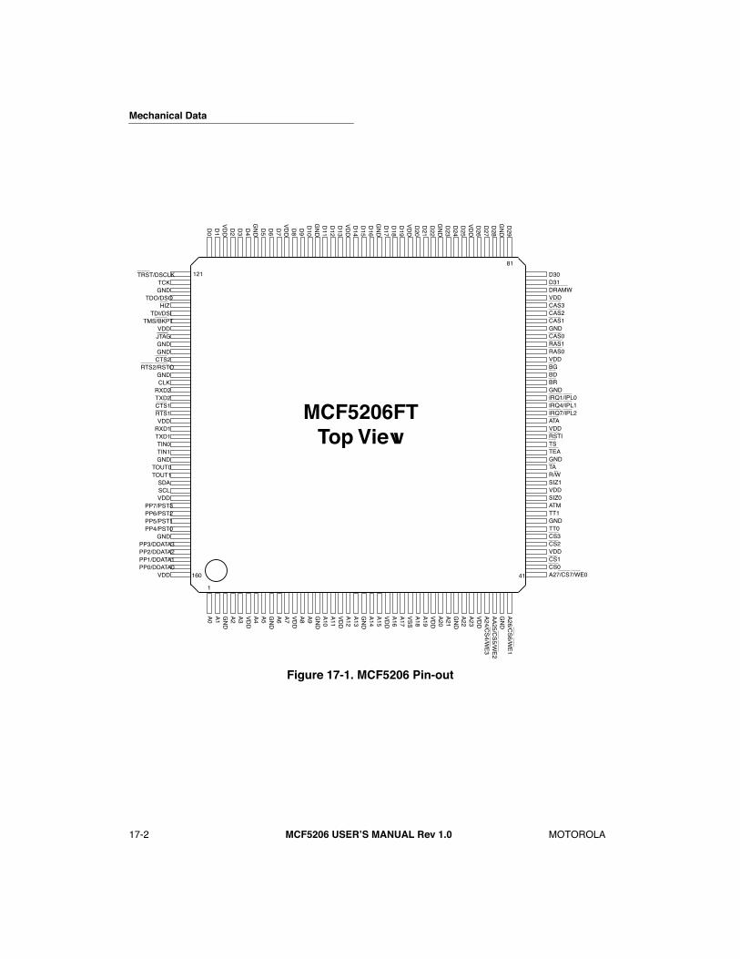
Mechanical Data
17-2
MCF5206 USERÕS MANUAL Rev 1.0
MOTOROLA
Figure 17-1. MCF5206 Pin-out
�
MCF5206FT�Top View
TRST/DSCLK�TCK�GND�
TDO/DSO�HIZ�
TDI/DSI�TMS/BKPT�
VDD�JTAG�GND�GND�CTS2�
RTS2/RSTO�GND�CLK�RXD2�TXD2�CTS1�RTS1�VDD�RXD1�TXD1�TIN0�TIN1�GND�
TOUT0�TOUT1�SDA�SCL�VDD�
PP7/PST3�PP6/PST2�PP5/PST1�PP4/PST0�
GND�PP3/DDATA3�PP2/DDATA2�PP1/DDATA1�PP0/DDATA0�
VDD��
D30�D31�DRAMW�VDD�CAS3�CAS2�CAS1�GND�CAS0�RAS1�RAS0�VDD�BG�BD�BR�GND�IRQ1/IPL0�IRQ4/IPL1�IRQ7/IPL2�ATA�VDD�RSTI�TS�TEA�GND�TA�R/W�SIZ1�VDD�SIZ0�ATM�TT1�GND�TT0�CS3�CS2�VDD�CS1�CS0�A27/CS7/WE0��
A26/C
S6/W
E1�
GND�
AA25/C
S5/W
E2�
A24/C
S4/W
E3�
VDD�
A23�A22�GND�
A21�A20�VDD�
A19�A18�VSS�
A17�A16�VDD�
A15�A14�GND�
A13�A12�VDD�
A11�A10�GND�
A9�A8�VDD�
A7�A6�GND�
A5�A4�VDD�
A3�A2�GND�
A1�A0
D29�
GND�
D28�D27�D26�
VDD�
D25�D24�D23�
GND�
D22�D21�D20�
VDD�
D19�D18�D17�
GND�
D16�D15�D14�
VDD�
D13�D12�D11�
GND�
D10�D9�D8�
VDD�
D7�D6�D5�
GND�
D4�D3�D2�
VDD�
D1�D0
1
41
81
121
160
�
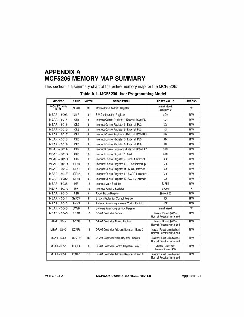
MOTOROLA
MCF5206 USERÕS MANUAL Rev 1.0
Appendix A-1
B
C
D
E
F
G
H
I
J
K
L
M
N
O
P
A
APPENDIX AMCF5206 MEMORY MAP SUMMARY
This section is a summary chart of the entire memory map for the MCF5206.
Table A-1. MCF5206 User Programming Model
ADDRESS NAME WIDTH DESCRIPTION RESET VALUE ACCESS
MOVEC with $C0F
MBAR 32 Module Base Address Register uninitialized(except V=0) W
MBAR + $003
SIMR 8 SIM Configuration Register $C0 R/W
MBAR + $014
ICR1 8 Interrupt Control Register 1 - External IRQ1/IPL1 $04 R/W
MBAR + $015
ICR2 8 Interrupt Control Register 2 - External IPL2 $08 R/W
MBAR + $016
ICR3 8 Interrupt Control Register 3 - External IPL3 $0C R/W
MBAR + $017
ICR4 8 Interrupt Control Register 4 - External IRQ4/IPL4 $10 R/W
MBAR + $018
ICR5 8 Interrupt Control Register 5 - External IPL5 $14 R/W
MBAR + $019
ICR6 8 Interrupt Control Register 6 - External IPL6 $18 R/W
MBAR + $01A
ICR7 8 Interrupt Control Register 7 - External IRQ7/IPL7 $1C R/W
MBAR + $01B
ICR8 8 Interrupt Control Register 8 - SWT $1C R/W
MBAR + $01C
ICR9 8 Interrupt Control Register 9 - Timer 1 Interrupt $80 R/W
MBAR + $01D
ICR10 8 Interrupt Control Register 10 - Timer 2 Interrupt $80 R/W
MBAR + $01E
ICR11 8 Interrupt Control Register 11 - MBUS Interrupt $80 R/W
MBAR + $01F
ICR12 8 Interrupt Control Register 12 - UART 1 Interrupt $00 R/W
MBAR + $020
ICR13 8 Interrupt Control Register 13 - UART2 Interrupt $00 R/W
MBAR + $036
IMR 16 Interrupt Mask Register $3FFE R/W
MBAR + $03A
IPR 16 Interrupt Pending Register $0000 R
MBAR + $040
RSR 8 Reset Status Register $80 or $20 R/W
MBAR + $041
SYPCR 8 System Protection Control Register $00 R/W
MBAR + $042
SWIVR 8 Software Watchdog Interrupt Vector Register $0F R/W
MBAR + $043
SWSR 8 Software Watchdog Service Register uninitialized W
MBAR + $046
DCRR 16 DRAM Controller Refresh Master Reset: $0000Normal Reset: uninitialized
R/W
MBAR + $04A DCTR 16 DRAM Controller Timing Register Master Reset: $0000Normal Reset: uninitialized
R/W
MBAR + $04C DCAR0 16 DRAM Controller Address Register - Bank 0 Master Reset: uninitializedNormal Reset: uninitialized
R/W
MBAR + $050 DCMR0 32 DRAM Controller Mask Register - Bank 0 Master Reset: uninitializedNormal Reset: uninitialized
R/W
MBAR + $057 DCCR0 8 DRAM Controller Control Register- Bank 0 Master Reset: $00Normal Reset: $00
R/W
MBAR + $058 DCAR1 16 DRAM Controller Address Register - Bank 1 Master Reset: uninitializedNormal Reset: uninitialized
R/W

Appendix A
Appendix A-2
MCF5206
USERÕS MANUAL Rev 1.0
MOTOROLA
B
C
D
E
F
G
H
I
J
K
L
M
N
O
P
A
MBAR + $05C DCMR1 32 DRAM Controller Mask Register - Bank 1 Master Reset: uninitializedNormal Reset: uninitialized
R/W
MBAR + $063 DCCR1 8 DRAM Controller Control Register - Bank 1 Master Reset: $00Normal Reset: $00
R/W
MBAR + 64 CSAR0 16 Chip-Select Address Register - Bank 0 0000 R/W
MBAR + 68 CSMR0 32 Chip-Select Mask Register - Bank 0 00000000 R/W
MBAR + $06E CSCR0 16 Chip-Select Control Register - Bank 0
3C1F, 3C5F, 3C9F, 3CDF, 3D1F, 3D5F, 3D9F, or 3DDF
AA set by IRQ7 at resetPS1 set by IRQ4 at resetPS0 set by IRQ1 at reset
R/W
MBAR + $070 CSAR1 16 Chip-Select Address Register - Bank 1 uninitialized R/W
MBAR + $074 CSMR1 32 Chip-Select Mask Register - Bank 1 uninitialized R/W
MBAR + $07A CSCR1 16 Chip-Select Control Register - Bank 1uninitialized
(except BRST=ASET=WRAH=RDAH=
WR=RD=0)R/W
MBAR + $07C CSAR2 16 Chip-Select Address Register - Bank 2 uninitialized R/W
MBAR + $080 CSMR2 32 Chip-Select Mask Register - Bank 2 uninitialized R/W
MBAR + $086 CSCR2 16 Chip-Select Control Register - Bank 2uninitialized
(except BRST=ASET=WRAH=RDAH=
WR=RD=0)R/W
MBAR + $088 CSAR3 16 Chip-Select Address Register - Bank 3 uninitialized R/W
MBAR + $08C CSMR3 32 Chip-Select Mask Register - Bank 3 uninitialized R/W
MBAR + $092 CSCR3 16 Chip-Select Control Register - Bank 3uninitialized
(except BRST=ASET=WRAH=RDAH=
WR=RD=0)R/W
MBAR + $094 CSAR4 16 Chip-Select Address Register - Bank 4 uninitialized R/W
MBAR + $098 CSMR4 32 Chip-Select Mask Register - Bank 4 uninitialized R/W
MBAR + $09E CSCR4 16 Chip-Select Control Register - Bank 4uninitialized
(except BRST=ASET=WRAH=RDAH=
WR=RD=0)R/W
MBAR + $0A0 CSAR5 16 Chip-Select Address Register - Bank 5 uninitialized R/W
MBAR + $0A4 CSMR5 32 Chip-Select Mask Register - Bank 5 uninitialized R/W
MBAR + $0AA CSCR5 16 Chip-Select Control Register - Bank 5uninitialized
(except BRST=ASET=WRAH=RDAH=
WR=RD=0)R/W
MBAR + $0AC CSAR6 16 Chip-Select Address Register - Bank 6 uninitialized R/W
MBAR + $0B0 CSMR6 32 Chip-Select Mask Register - Bank 6 uninitialized R/W
MBAR + $0B6 CSCR6 16 Chip-Select Control Register - Bank 6uninitialized
(except BRST=ASET=WRAH=RDAH=
WR=RD=0)R/W
MBAR + $0B8 CSAR7 16 Chip-Select Address Register - Bank 7 uninitialized R/W
MBAR + $0BC CSMR7 32 Chip-Select Mask Register - Bank 7 uninitialized R/W
MBAR + $0C2 CSCR7 16 Chip-Select Control Register - Bank 7uninitialized
(except BRST=ASET=WRAH=RDAH=
WR=RD=0)R/W
MBAR + $0C6 DMCR 16 Default Memory Control Register 0000 R/W
ADDRESS NAME WIDTH DESCRIPTION RESET VALUE ACCESS

Appendix A
MOTOROLA
MCF5206 USERÕS MANUAL Rev 1.0
Appendix A-3
B
C
D
E
F
G
H
I
J
K
L
M
N
O
P
A
MBAR + $0CB
PAR 8 Pin Assignment Register $00 R/W
MBAR+$100
TMR1 16 Timer1 Mode Register $0000 R/W
MBAR+$104
TRR1 16 Timer1 Reference Register $FFFF R/W
MBAR+$108
TCR1 16 Timer1 Capture Register $0000 R
MBAR+$10C
TCN1 16 Timer1 Counter $0000 R/W
MBAR+$111
TER1 8 Timer1 Event Register $00 R/W
MBAR+$120
TMR2 16 Timer2 Mode Register $0000 R/W
MBAR+$124
TRR2 16 Timer2 Reference Register $FFFF R/W
MBAR+$128
TCR2 16 Timer2 Capture Register $0000 R
MBAR+$12C
TCN2 16 Timer2 Counter $0000 R/W
MBAR+$131
TER2 8 Timer2 Event Register $00 R/W
MBAR + $140
UMR1,2 8 UART1 Mode Registers $00 R/W
MBAR+$144
USR/UCSR 8 UART1 Status Register (R/W=1)/ UART1 Clock-
Select Register (R/W=0) USR=$00; UCSR=$DD USR=R; UC-SR=W
MBAR+$148
UCR 8 UART1 Command Register $00 W
MBAR+$14C
URB/UTB 8 UART1 Receive Buffer (R/W=1)/ UART1 Transmit Buffer (R/W=0) URB=$FF; UTB=$00 URB=R;
UTB=W
MBAR+$150
UIPCR/UACR 8 UART Input Port Change Register (R/w=1);/
UART1 Auxilary Control Register (R/W=0) UIPCR=$0F; UACR=$00 UIPCR=R; UACR=W;
MBAR+$154
UISR/ UIMR 8 UART1 Interrupt Status Register (R/W=1);
UART1 Interrupt Mask Register (R/W=0) UISR=$00; UIMR=$00 UISR=R; UIMR=W
MBAR+$158
UBG1 8 UART1 Baud Rate Generator Prescale MSB uninitialized W
MBAR+$15C
UBG2 8 UART1 Baud Rate Generator Prescale LSB uninitialized W
MBAR+$170
UIVR 8 UART1 Interrupt Vector Register $0F R/W
MBAR+$174
UIP 8 UART1 Input Port Register $FF R
MBAR+$178
UOP1 8 UART1 Output Port Bit Set CMD UOP1[7:1]= undefined; UOP1=0 W
MBAR+$17C
UOP0 8 UART1 Output Port Bit Reset CMD uninitialized W
MBAR+$180
UMR1,2 8 UART2 Mode Registers $00 R/W
MBAR+$184
USR/UCSR 8 UART2 Status Register (R/W=1)/ UART1 Clock-
Select Register (R/W=0) USR=$00; UCSR=$DD USR=R; UC-SR=W
MBAR+$188
UCR 8 UART2 Command Register $00 W
MBAR+$18C
URB/UTB 8 UART2 Receive Buffer (R/W=1)/ UART1 Transmit Buffer (R/W=0) URB=$FF; UTB=$00 URB=R;
UTB=W
MBAR+$190
UIPCR/UACR 8 UART2 Input Port Change Register (R/w=1);/
UART1 Auxilary Control Register (R/W=0) UIPCR=$0F; UACR=$00 UIPCR=R; UACR=W;
MBAR+$194
UISR/ UIMR 8 UART2 Interrupt Status Register (R/W=1);
UART1 Interrupt Mask Register (R/W=0) UISR=$00; UIMR=$00 UISR=R; UIMR=W
MBAR+$198
UBG1 8 UART2 Baud Rate Generator Prescale MSB uninitialized R/W
MBAR+$19C
UBG2 8 UART2 Barud Rate Generator Prescale LSB uninitialized R/W
MBAR+$1B0
UIVR 8 UART2 Interrupt Vector Register $0F R/W
MBAR+$1B4
UIP 8 UART2 Input Port Register $FF R
MBAR+$1B8
UOP1 8 UART2 Output Port Bit Set CMD UOP1[7:1]= undefined; UOP1=0 W
MBAR+$1BC
UOP0 8 UART2 Output Port Bit Reset CMD uninitialized W
MBAR + $1C5
PPDDR 8 Port A Data Direction Register $00 R/W
MBAR + $1C9
PPDAT 8 Port A Data Register $00 R/W
MBAR+$1E0
MADR 8 M-Bus Address Register $00 R/W
ADDRESS NAME WIDTH DESCRIPTION RESET VALUE ACCESS
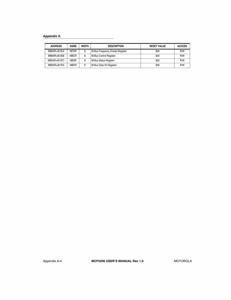
Appendix A
Appendix A-4
MCF5206
USERÕS MANUAL Rev 1.0
MOTOROLA
B
C
D
E
F
G
H
I
J
K
L
M
N
O
P
A
MBAR+$1E4
MFDR 8 M-Bus Frequency Divider Register $00 R/W
MBAR+$1E8
MBCR 8 M-Bus Control Register $00 R/W
MBAR+$1EC
MBSR 8 M-Bus Status Register $00 R/W
MBAR+$1F0
MBDR 8 M-Bus Data I/O Register $00 R/W
ADDRESS NAME WIDTH DESCRIPTION RESET VALUE ACCESS
MOTOROLA
MCF5206 USERÕS MANUAL Rev 1.0
Appendix B-1
C
D
E
F
G
H
I
J
K
L
M
N
O
P
A
APPENDIX BPORTING FROM M68K ARCHITECTURE
This section is an overview of the issues encountered when porting embedded development tools to work with the ColdFire processor when starting with the M68K architecture.
B.1 C COMPILERS AND HOST SOFTWARE
For the purpose of this discussion, it is assumed that an embedded software development tool chain consists of a ÒhostÓ portion and a ÒtargetÓ portion. The host portion consists of tool chain parts that execute on a desktop computer or workstation. The target portion of the tool chain runs ColdFire executables on a physical ColdFire target board.
Compilers, assemblers, linkers, loaders, instruction set simulators, and the host portion of debuggers are examples of host tools. Many host tools such as linkers and loaders that work with the M68K architecture can also be used without modification with ColdFire.
Although you can use an existing M68K assembler and disassembler with ColdFire, Motorola recommends modifying the assembler so that nonColdFire assembly code cannot be put together in the executable. This is especially true if the assembler assembles handwritten code. Porting the disassembler is for convenience and can be performed later.
Debuggers usually are comprised of two parts. A host portion of the debugger typically issues higher level commands for the target portion of debugger target. The target portion of the debugger typically handles the exact details of the implementation of tracing, breakpoints, and other lower level details. The debugger host portion requires little modification. Most likely, the only architectural items of concern are the following:
¥ Differences in the designed supervisor registers and stack pointers (for displaying registers)
¥ Interpretation of exception stack frames (if not already performed by the target portion)
B.2 TARGET SOFTWARE PORT
Porting ROM monitors and operating systems can begin after the compiler and assembler have been ported. For example, consider the steps involved in porting a ROM debugger. Similar issues are encountered when porting an RTOS and target applications.
It is assumed that target software consists of C and assembly source code. The first step is to create executables that will run on existing M68K hardware to test the conversion from M68K code to the proper ColdFire subset. This step verifies that the process of code conversion does not introduce new errors.
Appendix B
Appendix B-2
MCF5206
USERÕS MANUAL Rev 1.0
MOTOROLA
B
C
D
E
F
G
H
I
J
K
L
M
N
O
P
A
To generate a ColdFire executable of the target debugger, you should use a ColdFire-compliant port of the same C compiler originally used to create the M68K debugger target. This procedure prevents differences in calling convention and parameter passing from C to handwritten assembly. Another advantage to this approach is that special C flags are retained. Many C compilers have special extensions as well.
Whichever approach is used, the assembly language lines that are outside the ColdFire instruction set must be identified. Any ColdFire assembler that properly flags nonColdFire instructions can be used. During the process of conversion, you can ignore architectural issues temporarily because the target is still an M68K.
Once the instruction set differences have been resolved, the architectural differences between the ColdFire and M68K need to be addressed.
B.3 INITIALIZATION CODE
The target software and firmware often execute code that identifies the type of processor. Such a process provides one port that works with various M68K Family members and implementations. The easiest way to identify the ColdFire architecture from other M68K processors is to execute an ILLEGAL opcode ($4AFC). This execution generates an exception stack frame while ensuring that the tracing is disabled. The first two bits of the exception stack frame would immediately determine whether the processor is a ColdFire processor.
Motorola suggests that ColdFire architecture testing be performed immediately to avoid executing potentially undefined opcodes in the ColdFire architecture. Unused opcodes in the ColdFire architecture are not guaranteed to result in an illegal instruction exception.
Another item to consider is that the ColdFire architecture will have integrated versions with modules yet to be defined. It may be a good idea to ensure that there are enough hooks to allow for initialization of routines.
B.4 EXCEPTION HANDLERS
When dealing with exceptions in debug-oriented software, it is often necessary to extract exception stack information to obtain the SR and PC. The format word (MC68010 and higher) is typically used by generalized exception routines. Their sole purpose is to catch unexpected exceptions and to easily use vector information to identify the cause of the exception. The MC68000 exception frame is different from that of other members of the M68K processors in that there is no notion of a format word. This difference would have forced target software to deal with exception stack frame differences already. The approach now in use provides guidance on handling ColdFire exception stack frame differences. In many low-level exception handlers, the extraction of the stacked SR, PC, or format word is performed in a common source file or the offsets are handled in some type of header file.
Interrupt handlers probably require no modification because in most cases, an interrupt occurs asynchronously with respect to normal program flow. Therefore, interrupt handlers cannot rely on items on the stack as it is often unnecessary to know exactly what was happening at the time of the interrupt.
Appendix B
MOTOROLA
MCF5206
USERÕS MANUAL Rev 1.0
Appendix B-3
B
C
D
F
G
H
I
K
L
O
P
A
System calls are often implemented by using the TRAP instruction. For trap exceptions, parameter passing is performed through data and address registersÑrarely, if ever, directly through the stack. In addition, a system call typically does not need to know the stacked SR or PC information.
Breakpoints are usually implemented with the TRAP instruction or an illegal instruction such as an $A-line exception. If so, the stacked SR and PC are typically used. Other items in the stack may also need to be queried, especially if the breakpoint displays a stack trace. If so, you should examine the format closely for stack misalignments at the time of the breakpoint. This stack misalignment check would be useful in applications where stack alignment is a software design goal. These same concerns for the breakpoint implementation are applicable to trace exceptions as well.
A generalized exception handler can be implemented to catch unexpected exceptions. In addition to the SR and PC information, it is often necessary to obtain the vector information in the stack. Otherwise, the issues are similar to those found on breakpoints and tracing.
To port the ColdFire access error exception, it is best to start with an MC68000 bus error handler. The ColdFire access error recovery sequence has many similarities to the procedure recommended for the MC68000. However, you should be aware that a read bus error on the ColdFire will not advance the program counter to the next instruction. In addition, a write bus error may be taken long after an instruction has been executed and the stacked program counter may not point to the offending instruction.The main cause of an address error exception in the M68K architecture is that program flow is forced to continue at an odd address boundary. In addition, an MC68000 reports an address error if a data byte access is initiated on an odd address. The ColdFire uses the address error for implementations that do not have the misalignment module. A misaligned data access is then initiated. Modification of the address error exception handler to reflect a ColdFire misalignment exception is optional. The MCF5202 contains hardware support for data misalignment and therefore this is not an issue for family members.
On a ROM monitor, it is often necessary to provide a means by which a user program is executed given a certain starting address. This is often implemented by placing an exception stack frame and then performing an RTE. If this is the case, the header files that define what a stack frame looks like would require modification to reflect the ColdFire stack frame format.
B.5 SUPERVISOR REGISTERS
The target software would eventually need to communicate the contents of registers to the host software. Both the host portions and target portions of a debugger must be modified to reflect the single stack pointer architecture of ColdFire. In addition, the target debugger must keep a copy of the MOVEC register images in memory so that it can provide the host software register contents when asked to do so. A UNIX
grep
utility can find all instances of the MOVEC instruction and perform the appropriate modifications to accommodate the unidirectional MOVEC instruction.
The ColdFire architecture does not distinguish between a supervisor stack and a user stack. There is only a single stack pointer, A7. One way of dealing with this issue is to emulate the

Appendix B
Appendix B-4
MCF5206
USERÕS MANUAL Rev 1.0
MOTOROLA
B
C
D
E
F
G
H
I
J
K
L
M
N
O
P
A
dual stacks by placing some code at the beginning and end portions of exception handlers to change the stack pointer contents, if necessary, during exceptions. This approach has the disadvantage that interrupt latency would be degraded because interrupts would have to be disabled during the stack-swapping process, but enable full flexibility of the 68K stack model.

MOTOROLA
MCF5206 USER’S MANUAL I-5
INDEX
PRE-FIN
AL DRAFT
INDEX
Symbols
)
6-2
,
6-9
,
8-3
,
10-1
,
10-2
,
10-3
,
10-4
description,
2-3
,
2-4
external master use
2-3
)
8-4
),
6-1
Numerics
)A
6-8
row address strobes (RAS
10-1
, A
6-8
,RAS
10-1
address bus (A
2-3
,
6-1
,
6-8
,
8-3
,
10-3
column address strobe (CAS
10-2
data bus (D
2-4
,
6-2
,
6-9
,
8-4
,
10-4
A
access errors
1-5
ACR0, ACR1
4-3
,
4-8
address hold
8-8
,
8-34
address setup
8-8
,
8-33
addressing mode
1-8
Addressing Modesindex sizing and scaling
1-8
program counter indirect
1-8
register indirect
1-8
alternate master transfers
6-68
,
10-41
asynchronous acknowledge
6-27
autovector
7-4
,
7-5
,
7-6
,
7-10
B
baud generator
11-5
block mode
11-11
,
11-18
break condition
11-9
burst page mode
10-32
,
10-47
,
10-54
,
10-57
burst transferfast page mode
10-20
normal mode
10-18
burst transfers
6-8
,
6-15
,
6-74
,
8-7
,
8-14
,
8-23
,
10-44
burst-inhibited transfer
6-21
bus arbitration
10-30
operation,
6-53
protocol,
6-53
,
6-61
signals,
2-11
bus error
6-51
bus lock
7-9
bus monitor
7-2
,
7-15
Bus Sizing
6-7
bus sizing
8-7
C
cache invalidation
4-3
CACR
4-3
,
4-6
CCR
3-3
character mode
11-11
,
11-18
chip select 0
8-8
Chip Select Address Register (CSAR0-CSAR7)
8-28
Chip-select 0
8-5
Chip-select 1
8-5
Chip-Select Control Register (CSCR0 - CSCR7)
8-31
Chip-Select Control Register 0 (CSCR0)
6-85
,
8-8
Chip-Select Mask Register (CSMR0-CSMR7)
8-29
chip-selects
7-16
,
8-1
access permission
8-6
alernate master operation,
8-21
description
2-4
programming model,
8-26
Commandformat,
14-10
Sequence Diagram
14-10
sequence diagram
14-9
D
DataRegisters
14-12
,
14-26
data formats of the ColdFire architecture and alsoprovides extended support for all the data for-mants of the M68000 family. Th
1-8
data transferalternate master,
6-68
asynchronous acknowledge write,
6-30
asynchronous-acknowledge
6-27
bursting read
6-32
bursting word-read,
6-15
,
6-17
bursting write
6-35
Index
I-6 MCF5206 USER’S MANUAL MOTOROLA
INDEX
PRE-FIN
AL DRAFT
bursting write,
6-18
burst-inhibited read,
6-21
,
6-39
burst-inhibited write
6-42
longword-read
6-11
longword-write
8-9
operation,
6-6
word-write
6-14
debug interrupt
14-36
debug moduleBDM connector
14-38
breakpoint
14-35
command set,
14-7
CPU32 functionality
14-4
processor status,
14-2
programming model,
14-27
real-time debug
14-27
serial interface,
14-6
signals,
2-16
Default Memory
8-40
default memory
8-37
Default Memory Control Register (DMCR)
8-37
double bus fault
6-5
DRAMaccess permissions,
10-7
alternate master use
10-40
,
10-50
,
10-60
burst page mode
10-47
burst page mode,
10-32
,
10-54
bus arbitration,
10-30
fast page mode
10-50
,
10-54
,
10-56
,
10-57
fast page mode operation,
10-20
initialization
10-61
limitations
10-50
normal mode
10-54
normal mode operation
10-15
normal mode,
10-41
,
10-44
page hit,
10-23
,
10-25
page miss,
10-27
programming model
10-51
refresh operation,
10-38
signals,
2-13
DRAM Controller Address Registers (DCAR0-1)
10-58
DRAM Controller Control Register (DCCR0-1)
10-60
DRAM Controller Mask Register (DCMR0-1)
10-59
DRAM Controller Refresh Register (DCRR)
10-51
DRAM Controller Timing Register (DCTR)
10-52
E
EDO DRAM
10-35
,
10-53
,
10-56
,
10-57
exceptionsaccess errors,
1-5
bus,
6-5
external bus master
6-53
F
fast page mode
10-20
,
10-27
,
10-50
,
10-54
,
10-56
,
10-57
FIFO stack
11-11
fill buffer
4-1
H
halt
14-5
I
implicit ownership state
6-60
index sizing, index scaling, program counter indi-rect, register indirect
1-8
InstructionsSTOP
1-5
TRAP
1-5
internal reset
6-81
,
6-84
interrupt acknowledge cycles
6-47
,
6-48
,
11-16
Interrupt Control Register (ICR)
7-9
interrupt exception
6-47
Interrupt Mask Register (IMR)
7-11
interrupt masking
6-47
interrupt signals
2-7
Interrupt-Pending Register (IPR)
7-12
interrupts
1-5
external,
7-4
,
7-6
handling
11-33
M-BUS
7-5
requests (UART)
11-3
software watchdog
7-5
software watchdog,
7-3
spurious,
7-2
timer
7-5
UART,
7-5
J
JTAGboundary-scan register,
15-6
BYPASS instruction,
15-5
CLAMP instruction
15-5
HIGHZ instruction,
15-4
IDCODE instruction,
15-4
IDcode register,
15-5
SAMPLE/PRELOAD instruction
15-4
signals,
2-18
L
logical address space
1-8

Index
MOTOROLA MCF5206 USER’S MANUAL I-7
INDEX
PRE-FIN
AL DRAFT
looping modes
11-12
low-power stop mode
1-5
M
MADR
12-6
master reset
6-81
,
6-82
,
10-4
,
10-5
MBAR
7-1
,
7-7
,
10-62
MBCR
12-8
MBDR
12-11
MBSR
12-9
M-Busaddress register
12-6
arbitration lost
12-15
arbitration procedure
12-4
clock stretching
12-5
clock synchronization
12-5
control register
12-8
data I/O register
12-11
data transfer
12-4
frequency divider register
12-6
generation of repeated START
12-14
generation of START
12-11
generation of STOP
12-14
handshaking
12-5
initialization sequence
12-11
post-transfer software
12-12
programming examples
12-11
programming model
12-6
protocol
12-3
repeated START signal
12-4
slave address transmission
12-3
slave mode
12-15
START signal
12-3
status register
12-9
STOP signal
12-4
system configuration
12-2
M-businterrupts,
7-5
signals,
2-16
MC68040Vlow-power stop mode
1-5
MC68EC040Vlow-power stop mode
1-5
MFDR
12-6
multidrop mode
11-14
,
11-18
N
normal mode
10-15
,
10-41
,
10-44
,
10-54
normal reset
6-81
,
6-83
,
10-5
O
operand size
1-8
operation
6-8
overrun
11-12
,
11-18
,
11-22
P
parallel portsignals,
2-16
,
7-16
Pin Assignment Register (PAR)
7-16
port size
6-7
,
8-7
,
8-33
power dissipation
5-4
power management
5-4
privilege modes
1-5
Processing Statesnormal, exception, halted
1-4
processing statesexception,
1-4
halted
1-5
normal,
1-4
stopped
1-5
processor
1-4
PROGRAMMING
1-5
programming model
1-5
,
3-2
cache,
4-5
chip-selects,
8-26
debug model,
14-27
DRAM
10-51
parallel port,
9-1
supervisor
1-7
UART,
11-16
user
1-7
R
RAMBAR
5-2
ReadMemory Location Command
14-9
real-time trace
14-1
refresh rate
10-38
,
10-52
,
10-56
Registersaddress registers
1-7
condition code register
1-7
index registers
1-7
program counter
1-7
stack pointer
1-7
Status Register (SR)S-bit
1-5
vector base register
1-7
resetcache,
4-4
operation
6-81
operation,
10-4
Index
I-8 MCF5206 USER’S MANUAL MOTOROLA
INDEX
PRE-FIN
AL DRAFT
RSTI pin
6-83
,
14-5
RSTI pin,
2-12
,
6-82
RSTO pin
2-13
,
6-82
,
6-83
,
6-84
Reset Status Register (RSR)
7-13
reset, description,
2-12
S
SIM Configuration Register (SIMR)
7-9
Software Watchdog Interrupt Vector Register(SWIVR)
7-15
Software Watchdog Service Register (SWSR)
7-16
software watchdog timer
6-84
,
7-3
,
7-7
,
7-15
Special Modes of Operationlow-power stop mode
1-5
spurious interrupts
7-2
SR
3-4
supervisor programming model
1-6
System Protection Control Register (SYPCR)
7-2
,
7-14
system reset
7-2
T
three-wire mode
6-61
timer
11-3
interrupts,
7-5
Timer Capture Register (TCR)
13-5
Timer Counter (TCN)
13-5
Timer Event Regiser (TER)
13-6
Timer Mode Register (TMR)
13-4
timer module
13-1
block diagram
13-2
general-purpose timer units
13-2
Timer Reference Register (TRR)
13-5
two-wire mode
6-53
U
UARTbus operation,
11-16
interrupt acknowledge cycles,
11-16
interrupts,
7-5
programming model
11-16
signals,
2-15
UART Auxiliary Control Register (UACR)
11-29
UART Clock-Select Register (UCSR)
11-24
UART Command Register (UCR)
11-24
UART command register (UCR)
11-6
,
11-9
UART Input Port Change Register (UIPCR)
11-28
UART Input Port Register (UIP)
11-32
UART Interrupt Mask Register (UIMR)
11-30
UART Interrupt Status Register (UISR)
11-29
UART Interrupt Vector Register (UIVR)
11-31
UART Mode Register 1 (UMR1)
11-17
UART Mode Register 2 (UMR2)
11-19
UART moduleI/O driver routines
11-33
initialization routines
11-33
timer upper preload registers
11-31
timer/counter
11-3
valid start bit
11-9
UART Output Port Data Register (UOP0-1)
11-32
UART Receive Buffer (URB)
11-28
UART Status Register (USR)
11-21
UART Transmitter Buffer (UTB)
11-28
UBG1, 2
11-31
user programming model
1-6
V
VBR
3-5
W
write enables
2-5
,
7-16
,
8-1
encoding,
8-2