MC34673, High Input Voltage 1.2A Charger for Single … Integrated Circuit Device Data 6 Freescale...
22
Document Number: MC34673 Rev. 1.0, 01/2008 Freescale Semiconductor Advance Information * This document contains certain information on a new product. Specifications and information herein are subject to change without notice. © Freescale Semiconductor, Inc., 2007-8. All rights reserved. High Input Voltage 1.2A Charger for Single-cell Li-Ion Batteries The MC34673 is a cost-effective fully-integrated battery charger for Li-Ion or Li-Polymer batteries. The high input voltage, up to 28V, eliminates the input over-voltage protection circuit required in handheld devices such as PDAs, cell phones, portable video game players and digital still cameras. A typical charge cycle includes trickle, constant-current (CC) and constant-voltage (CV) charge modes. The CC-mode current is programmable up to 1.2A with an external resistor. The voltage across the external resistor is also used to monitor the actual charge current. The constant voltage is fixed at 4.2V with 0.7% accuracy over a -20°C to 70°C temperature range. The trickle-mode current is preset to 20% of the CC-mode current when the battery voltage is lower than the trickle-mode threshold. The end-of-charge (EOC) current threshold is preset to 10% of the CC-mode current to save the board space and cost. A charge current thermal foldback feature limits the charge current when the IC internal temperature rises to a preset threshold. The MC34673 also protects the system with its input over-voltage protection (OVP) feature. In addition, the MC34673 has a 2.6V falling power-on-reset (POR) threshold, making it perfect to work with current limited power supplies. Three indication pins (PPR , CHG and FAST ) can be simply interfaced to a microprocessor or LEDs. When no power supply is connected, or when disabled, the charger draws less than 1.0µA leakage current from the battery. Features • No external MOSFET, reverse-blocking diode or current-sense resistor are required • Guaranteed maximum 1.2A programmable CC-mode current • ±0.7% voltage accuracy over -20°C to 70°C • ±6% current accuracy over -40°C to 85°C • 28V maximum voltage for the power input with 6.8V over-voltage protection threshold • 2.6V minimum input operating voltage • Trickle charge for fully discharged batteries • Charge current monitor • Charge current thermal foldback • Pb-free packaging designated by suffix code EP Figure 1. 34673 Simplified Application Diagram POWER MANAGEMENT IC EP SUFFIX (PB-FREE) 98ASA10774D 8-PIN UDFN 34673 ORDERING INFORMATION Device Temperature Range (T A ) Package MC34673AEP/R2 -40°C to 85°C 8-UDFN V IN ON OFF VIN GND CHG PPR EN BAT ISET FAST TO BATTERY TO MCU V IO 34673 C IN C OUT R ISET
Transcript of MC34673, High Input Voltage 1.2A Charger for Single … Integrated Circuit Device Data 6 Freescale...

Document Number: MC34673Rev. 1.0, 01/2008
Freescale Semiconductor Advance Information
High Input Voltage 1.2A Charger for Single-cell Li-Ion Batteries
The MC34673 is a cost-effective fully-integrated battery charger for Li-Ion or Li-Polymer batteries. The high input voltage, up to 28V, eliminates the input over-voltage protection circuit required in handheld devices such as PDAs, cell phones, portable video game players and digital still cameras.
A typical charge cycle includes trickle, constant-current (CC) and constant-voltage (CV) charge modes. The CC-mode current is programmable up to 1.2A with an external resistor. The voltage across the external resistor is also used to monitor the actual charge current. The constant voltage is fixed at 4.2V with 0.7% accuracy over a -20°C to 70°C temperature range. The trickle-mode current is preset to 20% of the CC-mode current when the battery voltage is lower than the trickle-mode threshold. The end-of-charge (EOC) current threshold is preset to 10% of the CC-mode current to save the board space and cost. A charge current thermal foldback feature limits the charge current when the IC internal temperature rises to a preset threshold. The MC34673 also protects the system with its input over-voltage protection (OVP) feature. In addition, the MC34673 has a 2.6V falling power-on-reset (POR) threshold, making it perfect to work with current limited power supplies. Three indication pins (PPR, CHG and FAST) can be simply interfaced to a microprocessor or LEDs. When no power supply is connected, or when disabled, the charger draws less than 1.0µA leakage current from the battery.
Features
• No external MOSFET, reverse-blocking diode or current-sense resistor are required• Guaranteed maximum 1.2A programmable CC-mode current• ±0.7% voltage accuracy over -20°C to 70°C• ±6% current accuracy over -40°C to 85°C• 28V maximum voltage for the power input with 6.8V over-voltage protection threshold• 2.6V minimum input operating voltage• Trickle charge for fully discharged batteries• Charge current monitor• Charge current thermal foldback• Pb-free packaging designated by suffix code EP
Figure 1. 34673 Simplified Application Diagram
POWER MANAGEMENT IC
EP SUFFIX (PB-FREE)98ASA10774D
8-PIN UDFN
34673
ORDERING INFORMATION
Device Temperature Range (TA) Package
MC34673AEP/R2 -40°C to 85°C 8-UDFN
VIN
ONOFF
VINGND
CHG
PPR
EN
BAT
ISET
FAST
TO BATTERY
TO MCU
VIO
34673
CINCOUT
RISET
* This document contains certain information on a new product. Specifications and information herein are subject to change without notice.
© Freescale Semiconductor, Inc., 2007-8. All rights reserved.

INTERNAL BLOCK DIAGRAM
INTERNAL BLOCK DIAGRAM
Figure 2. 34673 Simplified Internal Block Diagram
+
–Logic
+
–+
–+ –
+
–
+
–
DieTemp
110°C
IEOC
VIN
BAT
VOS IREF
VREF
REF
InternalVINMonitor
ChargeControl
BAT
ISET
FAST
VIN
PPR
CHG
EN
GND
Supply
Control
Analog Integrated Circuit Device Data 2 Freescale Semiconductor
34673

PIN CONNECTIONS
PIN CONNECTIONS
Figure 3. 34673 Pin Connections Table 1. 34673 Pin Definitions
A functional description of each pin can be found in the Functional Pin Description section beginning on page 11.
Pin Number Pin Name Pin Function Formal Name Definition
1 VIN Input Input supply The supply input.
2 PPR Output Power present indicator
Indication of the input power status. Open drain output.
3 CHG Output Charge indicator Indication of the charge status. Open drain output.
4 EN Input Enable Enable logic input.
5 GND Ground Ground Ground.
6 FAST Output Fast charge indicator Indication of the fast charge status. Open drain output.
7 ISET Output CC-mode current setting and charge
current monitor
CC-mode current setting and monitoring pin.
8 BAT Output Charger output The charger output pin. Connect this pin to the Li-Ion battery.
EPAD EPAD N/A Exposed pad Exposed pad for thermal dissipation enhancement. Must be soldered on the large ground plane on the PCB to increase the thermal dissipation. The pad must be connected to GND electrically.
BAT
ISET
FAST
GND
VIN
PPR
CHG
EN
EPAD
1
2
3
4
8
7
6
5
Analog Integrated Circuit Device Data Freescale Semiconductor 3
34673

ELECTRICAL CHARACTERISTICSMAXIMUM RATINGS
ELECTRICAL CHARACTERISTICS
MAXIMUM RATINGS
Table 2. Maximum Ratings
All voltages are with respect to ground unless otherwise noted. Exceeding these ratings may cause a malfunction or permanent damage to the device.
Ratings Symbol Value Unit
ELECTRICAL RATINGS
Input Voltage RangeVIN PinPPR and CHG PinsEN, BAT, ISET, and FAST Pins
VIN
VPPR, VCHG VEN, VBAT,
VISET, VFAST
-0.3 to 28-0.3 to 12-0.3 to 5.5
V
ESD Voltage(1)
Human Body Model (HBM)Machine Model (MM)
VESD ±2000±200
V
THERMAL RATINGS
Operating TemperatureAmbientJunction
TA
TJ
-40 to 85-40 to 150
°C
Storage Temperature TSTG -65 to +150 °C
Thermal Resistance(2)
Junction-to-CaseJunction-to-Ambient
RθJC RθJA
1070
°C/W
Peak Package Reflow Temperature During Reflow(3),(4) TPPRT Note 4 °C
Notes1. ESD testing is performed in accordance with the Human Body Model (HBM) (CZAP = 100pF, RZAP = 1500Ω), and the Machine Model
(MM) (CZAP = 200pF, RZAP = 0Ω).2. Device mounted on the Freescale EVB test board per JEDEC DESD51-2. 3. Pin soldering temperature limit is for 10 seconds maximum duration. Not designed for immersion soldering. Exceeding these limits may
cause malfunction or permanent damage to the device.4. Freescale’s Package Reflow capability meets Pb-free requirements for JEDEC standard J-STD-020C. For Peak Package Reflow
Temperature and Moisture Sensitivity Levels (MSL), Go to www.freescale.com, search by part number [e.g. remove prefixes/suffixes and enter the core ID to view all orderable parts. (i.e. MC33xxxD enter 33xxx), and review parametrics.
Analog Integrated Circuit Device Data 4 Freescale Semiconductor
34673
ELECTRICAL CHARACTERISTICSSTATIC ELECTRICAL CHARACTERISTICS
STATIC ELECTRICAL CHARACTERISTICS
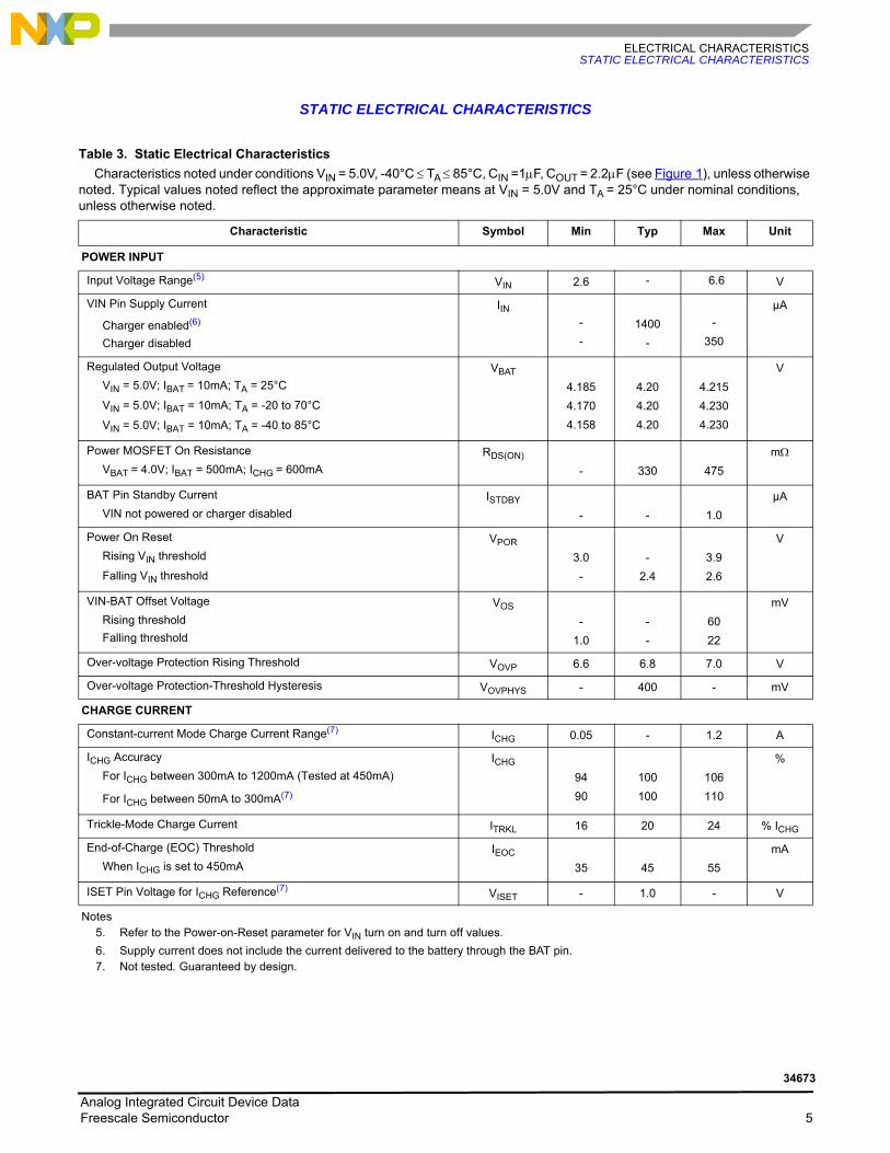
Table 3. Static Electrical Characteristics
Characteristics noted under conditions VIN = 5.0V, -40°C ≤ TA ≤ 85°C, CIN =1µF, COUT = 2.2µF (see Figure 1), unless otherwise noted. Typical values noted reflect the approximate parameter means at VIN = 5.0V and TA = 25°C under nominal conditions, unless otherwise noted.
Characteristic Symbol Min Typ Max Unit
POWER INPUT
Input Voltage Range(5) VIN 2.6 - 6.6 V
VIN Pin Supply Current
Charger enabled(6)
Charger disabled
IIN--
1400-
-350
µA
Regulated Output VoltageVIN = 5.0V; IBAT = 10mA; TA = 25°C
VIN = 5.0V; IBAT = 10mA; TA = -20 to 70°C
VIN = 5.0V; IBAT = 10mA; TA = -40 to 85°C
VBAT
4.1854.1704.158
4.204.204.20
4.2154.2304.230
V
Power MOSFET On ResistanceVBAT = 4.0V; IBAT = 500mA; ICHG = 600mA
RDS(ON)
- 330 475mΩ
BAT Pin Standby CurrentVIN not powered or charger disabled
ISTDBY
- - 1.0µA
Power On ResetRising VIN threshold
Falling VIN threshold
VPOR
3.0-
-2.4
3.92.6
V
VIN-BAT Offset VoltageRising thresholdFalling threshold
VOS
-1.0
--
6022
mV
Over-voltage Protection Rising Threshold VOVP 6.6 6.8 7.0 V
Over-voltage Protection-Threshold Hysteresis VOVPHYS - 400 - mV
CHARGE CURRENT
Constant-current Mode Charge Current Range(7) ICHG 0.05 - 1.2 A
ICHG AccuracyFor ICHG between 300mA to 1200mA (Tested at 450mA)
For ICHG between 50mA to 300mA(7)
ICHG
9490
100100
106110
%
Trickle-Mode Charge Current ITRKL 16 20 24 % ICHG
End-of-Charge (EOC) Threshold When ICHG is set to 450mA
IEOC
35 45 55mA
ISET Pin Voltage for ICHG Reference(7) VISET - 1.0 - V
Notes5. Refer to the Power-on-Reset parameter for VIN turn on and turn off values.6. Supply current does not include the current delivered to the battery through the BAT pin.7. Not tested. Guaranteed by design.
Analog Integrated Circuit Device Data Freescale Semiconductor 5
34673

ELECTRICAL CHARACTERISTICSSTATIC ELECTRICAL CHARACTERISTICS
CHARGE THRESHOLDS
Trickle-Mode Rising Threshold Voltage VTRKL 2.6 2.7 2.8 V
Trickle-Mode Threshold Voltage Hysteresis VTRKLHYS 40 100 150 mV
Recharge Threshold Voltage VRECH 4.060 4.100 4.140 V
Recharge Falling Threshold Voltage Hysteresis VTHRCHG - 25 50 mV
LOGIC INPUT AND OUTPUT
EN Input High Threshold Voltage VIH 1.5 - - V
EN Input Low Threshold Voltage VIL - - 0.5 V
EN Input Leakage Current VEN = 3.0V
IEN
- 2.0 7.5µA
PPR and CHG Sink Current When the Output is LowVCHG =VPPR = 0.6V
IPCSINKL12 15 -
mA
PPR and CHG Leakage Current When the Output is High-impedanceVCHG =VPPR = 5.0V
IPCLEAKH- - 1.0
µA
FAST Sink Current When the Output is LowVFAST = 0.5.0V
IFSINKL0.3 - -
mA
FAST Leakage Current When the Output is High-impedanceVFAST = 3.0V
IFLEAKH- - 1.0
µA
CHARGE CURRENT THERMAL FOLDBACK
Current Foldback Die Temperature Limit TLIMIT 95 110 125 °C
Table 3. Static Electrical Characteristics (continued)Characteristics noted under conditions VIN = 5.0V, -40°C ≤ TA ≤ 85°C, CIN =1µF, COUT = 2.2µF (see Figure 1), unless otherwise
noted. Typical values noted reflect the approximate parameter means at VIN = 5.0V and TA = 25°C under nominal conditions, unless otherwise noted.
Characteristic Symbol Min Typ Max Unit
Analog Integrated Circuit Device Data 6 Freescale Semiconductor
34673

ELECTRICAL CHARACTERISTICSDYNAMIC ELECTRICAL CHARACTERISTICS
DYNAMIC ELECTRICAL CHARACTERISTICS
Table 4. Dynamic Electrical Characteristics
Characteristics noted under conditions VIN = 5.0V, -40°C ≤ TA ≤ 85°C, CIN =1µF, COUT = 2.2µF (Figure 1), unless otherwise noted. Typical values noted reflect the approximate parameter means at VIN = 5.0V and TA = 25°C under nominal conditions, unless otherwise noted.
Characteristic Symbol Min Typ Max Unit
END OF CHARGE
EOC Filter Time tEOC 5.5 8.0 11 ms
OSCILLATOR
Oscillation Frequency fOSC 40.0 50.0 60.0 kHz
Analog Integrated Circuit Device Data Freescale Semiconductor 7
34673
ELECTRICAL CHARACTERISTICSELECTRICAL PERFORMANCE CURVES
ELECTRICAL PERFORMANCE CURVES
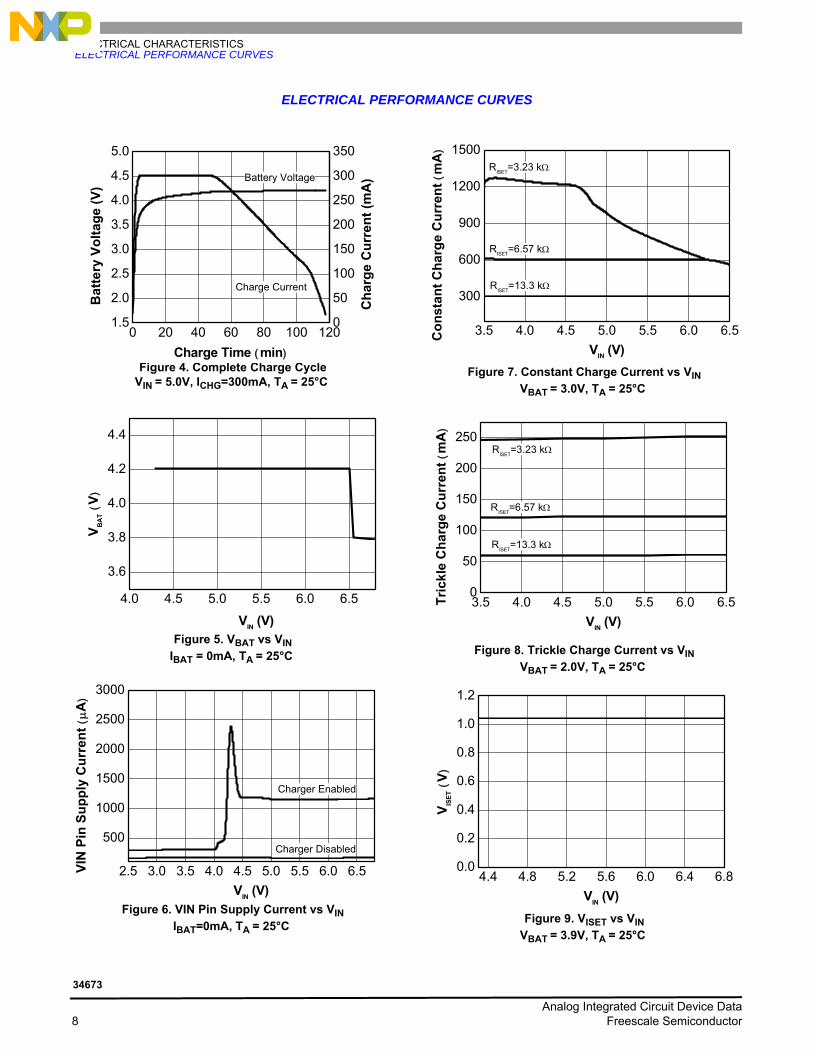
Figure 4. Complete Charge CycleVIN = 5.0V, ICHG=300mA, TA = 25°C
Figure 5. VBAT vs VINIBAT = 0mA, TA = 25°C
Figure 6. VIN Pin Supply Current vs VINIBAT=0mA, TA = 25°C
Figure 7. Constant Charge Current vs VINVBAT = 3.0V, TA = 25°C
Figure 8. Trickle Charge Current vs VINVBAT = 2.0V, TA = 25°C
Figure 9. VISET vs VINVBAT = 3.9V, TA = 25°C
0 20 40 60 80 100 1201.5
2.0
2.5
3.0
3.5
4.0
4.5
5.0
0
50
100
150
200
250
300
350
Cha
rge
Cur
rent
(mA
)
Charge Current
Bat
tery
Vol
tage
(V)
Charge Time (min)
Battery Voltage
4.0 4.5 5.0 5.5 6.0 6.5
3.6
3.8
4.0
4.2
4.4
V BA
T (V)
VIN (V)
2.5 3.0 3.5 4.0 4.5 5.0 5.5 6.0 6.5
500
1000
1500
2000
2500
3000
Charger Enabled
VIN
Pin
Sup
ply
Cur
rent
(µA
)
VIN (V)
Charger Disabled
3.5 4.0 4.5 5.0 5.5 6.0 6.5
300
600
900
1200
1500RISET=3.23 kΩ
RISET=6.57 kΩ
Con
stan
t Cha
rge
Cur
rent
(mA)
VIN (V)
RISET=13.3 kΩ
3.5 4.0 4.5 5.0 5.5 6.0 6.50
50
100
150
200
250
RISET=13.3 kΩ
RISET=3.23 kΩ
RISET=6.57 kΩ
Tric
kle
Cha
rge
Cur
rent
(m
A)
VIN (V)
4.4 4.8 5.2 5.6 6.0 6.4 6.80.0
0.2
0.4
0.6
0.8
1.0
1.2
V ISET
(V)
VIN (V)
Analog Integrated Circuit Device Data 8 Freescale Semiconductor
34673
ELECTRICAL CHARACTERISTICSELECTRICAL PERFORMANCE CURVES
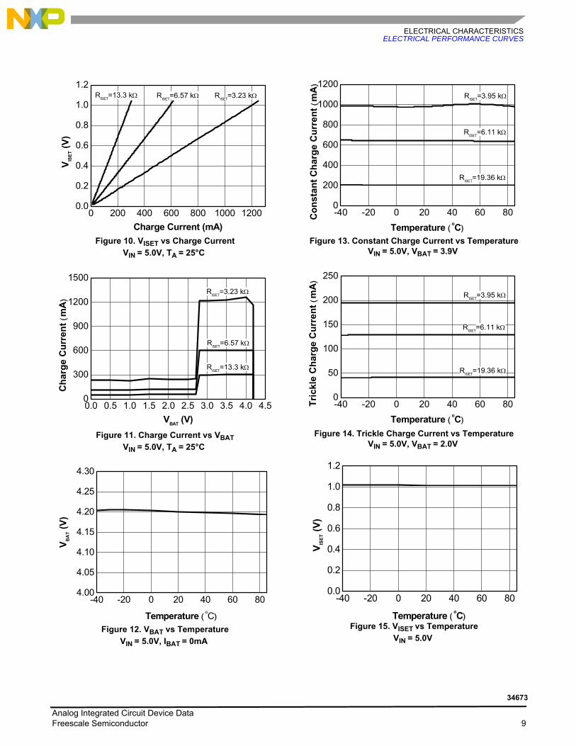
Figure 10. VISET vs Charge CurrentVIN = 5.0V, TA = 25°C
Figure 11. Charge Current vs VBATVIN = 5.0V, TA = 25°C
Figure 12. VBAT vs TemperatureVIN = 5.0V, IBAT = 0mA
Figure 13. Constant Charge Current vs TemperatureVIN = 5.0V, VBAT = 3.9V
Figure 14. Trickle Charge Current vs TemperatureVIN = 5.0V, VBAT = 2.0V
Figure 15. VISET vs TemperatureVIN = 5.0V
0 200 400 600 800 1000 12000.0
0.2
0.4
0.6
0.8
1.0
1.2RISET=3.23 kΩRISET=13.3 kΩ RISET=6.57 kΩ
V ISET
(V)
Charge Current (mA)
0.0 0.5 1.0 1.5 2.0 2.5 3.0 3.5 4.0 4.50
300
600
900
1200
1500
RISET=13.3 kΩ
RISET=3.23 kΩ
RISET=6.57 kΩ
Cha
rge
Cur
rent
(mA)
VBAT (V)
-40 -20 0 20 40 60 804.00
4.05
4.10
4.15
4.20
4.25
4.30
V BA
T (V)
Temperature ( oC)
-40 -20 0 20 40 60 800
200
400
600
800
1000
1200RISET=3.95 kΩ
RISET=19.36 kΩ
Con
stan
t Cha
rge
Cur
rent
(m
A)
Temperature ( oC)
RISET=6.11 kΩ
-40 -20 0 20 40 60 800
50
100
150
200
250
RISET=19.36 kΩ
RISET=3.95 kΩ
RISET=6.11 kΩ
Tric
kle
Cha
rge
Cur
rent
(m
A)
Temperature ( oC)
-40 -20 0 20 40 60 800.0
0.2
0.4
0.6
0.8
1.0
1.2
V ISET
(V)
Temperature ( oC)
Analog Integrated Circuit Device Data Freescale Semiconductor 9
34673
ELECTRICAL CHARACTERISTICSELECTRICAL PERFORMANCE CURVES
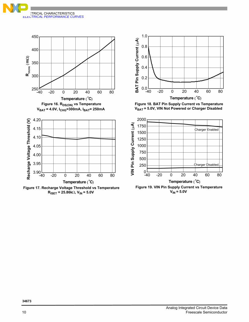
Figure 16. RDS(ON) vs TemperatureVBAT = 4.0V, ICHG=300mA, IBAT= 250mA
Figure 17. Recharge Voltage Threshold vs TemperatureRISET = 25.86kΩ, VIN = 5.0V
Figure 18. BAT Pin Supply Current vs TemperatureVBAT = 5.0V, VIN Not Powered or Charger Disabled
Figure 19. VIN Pin Supply Current vs TemperatureVIN = 5.0V
-40 -20 0 20 40 60 80250
300
350
400
450
RD
S(O
N) (
mΩ)
Temperature ( oC)
-40 -20 0 20 40 60 803.90
3.95
4.00
4.05
4.10
4.15
4.20
Rec
harg
e Vo
ltage
Thr
esho
ld (V
)
Temperature ( oC)
-40 -20 0 20 40 60 800.0
0.2
0.4
0.6
0.8
1.0
BA
T Pi
n Su
pply
Cur
rent
(µA
)
Temperature ( oC)
-40 -20 0 20 40 60 800
250500750
10001250150017502000
Charger EnabledVI
N P
in S
uppl
y C
urre
nt (µ
A)
Temperature ( oC)
Charger Disabled
Analog Integrated Circuit Device Data 10 Freescale Semiconductor
34673

FUNCTIONAL DESCRIPTIONINTRODUCTION
FUNCTIONAL DESCRIPTION
INTRODUCTION
The MC34673 is a fully-integrated Li-Ion and Li-Polymer battery charger in a tiny package. It uses current, voltage and temperature control loops to regulate the charge current. It has up to 28V input voltage rating, which makes the handheld device safe even when connected to a wrong AC adapter.
The MC34673 requires only two external capacitors and one resistor to build a fully functional charger for space-limited applications such as PDAs, cell phones, portable video game players and digital still cameras. Its ultra high-accuracy (±0.7%) output voltage and temperature-limited charging current offer additional battery safety during charging.
The CC-mode current can be programmed with an external resistor (RISET). The voltage across this resistor is proportional to the charge current, so the system can monitor the charge current during the whole charge cycle. The EOC current threshold is preset to 10% of the CC-mode current. For a deeply discharged battery with a voltage lower than 2.7V, the MC34673 charges the battery with a trickle-mode current, which is 20% of the CC-mode current.
Three indication outputs make it easy to report the input power status and the charge status to MCUs, or users via LEDs.
FUNCTIONAL PIN DESCRIPTION
INPUT SUPPLY (VIN)The supply input. This pin should be bypassed to ground
with a 1.0µF capacitor.
POWER PRESENT INDICATOR (PPR)Open-drain logic output to indicate the input power status.
The PPR-pin output is only determined by the input voltage, not other conditions such as the EN pin input. The output is low if VIN is higher than VPOR. This pin is capable to sink at least 12.0mA current to drive a LED indicator.
CHARGE INDICATOR (CHG)Open-drain logic output to indicate the charge status. The
output is low when the MC34673 is charging, until the EOC conditions are reached. This pin is capable to sink at least 12.0mA current to drive a LED indicator.
ENABLE (EN)Active-low enable logic Input. This pin is internally pulled
to ground by a weak current source. When left floating, the charger is enabled. Pulling this pin to high voltage externally disables the charger.
GROUND (GND)Ground.
FAST CHARGE INDICATOR (FAST)When charging, this open-drain logic output indicates
whether or not the battery voltage is higher than the trickle-
mode threshold. This pin is capable to sink more than 0.3mA current. When the charger is on, this pin outputs a logic low signal if the battery voltage is higher than the trickle-mode threshold. When the charger is in the shutdown mode or in any fault conditions, this pin outputs high-impedance.
CC-MODE CURRENT SETTING AND CHARGE CURRENT MONITOR (ISET)
The CC-mode current, ICHG, is programmed by connecting a resistor, RISET, between this pin and the ground. When charging in the CC-mode, the voltage at this pin is 1.0V. The voltage reduces proportionally as the charge current reduces in the CV-mode. During the whole charge cycle, the voltage at this pin can be used to monitor the charge current using the following equation:
equ. 1
where IBAT is the actual charge current, ICHG is the programmed CC-mode current, and VISET is the voltage of the ISET pin during the whole charge cycle.
CHARGER OUTPUT (BAT)Charger output pin. Connect this pin to the battery being
charged. Bypass to ground with a 2.2µF or higher capacitor.
EXPOSED PAD (EPAD)Exposed pad. Must be soldered on the large ground plane
on the PCB to enhance the thermal conductivity. The pad must be connected to GND electrically.
IBATVISET1.0V
--------------- ICHG⋅=
Analog Integrated Circuit Device Data Freescale Semiconductor 11
34673

FUNCTIONAL DESCRIPTIONFUNCTIONAL INTERNAL BLOCK DESCRIPTION
FUNCTIONAL INTERNAL BLOCK DESCRIPTION
Figure 20. 34673 Functional Internal Block Diagram
INTEGRATED SUPPLY
INTERNAL SUPPLY AND REFERENCEThis block steps down the high input voltage to a lower
voltage to power all the internal blocks. In addition, this block generates the reference voltage for the charge-control block.
SENSING AND CONTROL
VIN MONITORThe input voltage monitor block monitors the input voltage
for two thresholds, power-on-reset (POR) and over-voltage protection (OVP). If the input is lower than the POR or higher than the OVP threshold, this block outputs a logic signal to disable the charger.
CHARGE CONTROLThe charge-control block controls the gate voltage of the
power MOSFET to regulate the charge current, the battery voltage, or the die temperature. It can also completely turn off the power MOSFET to stop the current flow between the input and the battery. Also, monitoring of the charge current and the charger output voltage determines the trickle-charge mode and the recharge cycle.
CURRENT SETTING AND MONITORThis block programs the charge current in the constant-
current mode and monitors the actual charge current during the whole charge cycle.
EOC (END OF CHARGE)The EOC block monitors the charge current and the
battery voltage for the EOC conditions. Once the EOC conditions are reached, this block outputs a logic signal to indicate the end of the charge.
VIN-BAT COMPARATORThe VIN-BAT comparator monitors the voltage difference
between the input voltage and the battery voltage. The input voltage has to be higher than the battery voltage for the charger to be enabled. If the input voltage falls below the battery voltage, this block outputs a signal to disable the charger to prevent the leakage current from the battery to the input.
DIE TEMPERATURE FEEDBACKThe die temperature feedback block monitors the die
temperature. Once the die temperature reaches the threshold temperature, the charge-control block can reduce the charge current to prevent further die temperature rise.
MC34673 - Functional Block Diagram
Integrated Supply Sensing & Control MOSFET
Power MOSFET
Logic
Integrated Supply
Internal Supply & Reference
Sensing & Control
Logic
Die Temperature Feedback
Current Setting
Current Monitor
Status Indication
VIN - BAT Compare
VIN Monitor Charge Control
Logic Control
End of Charge
Analog Integrated Circuit Device Data 12 Freescale Semiconductor
34673

FUNCTIONAL DESCRIPTIONFUNCTIONAL INTERNAL BLOCK DESCRIPTION
LOGIC
LOGIC CONTROL AND STATUS INDICATIONThe logic control block determines the on and off of the
charger. It takes the signals from the VIN Monitor, VIN-BAT Comparator, EOC, and the external enable signal, and
determines the on and off states as well as the charge status indication outputs of the charger (CHG, PPR, and FAST).
POWER MOSFETThe power MOSFET passes the charging current from the
input to the output.
Analog Integrated Circuit Device Data Freescale Semiconductor 13
34673

FUNCTIONAL DEVICE OPERATIONOPERATIONAL MODES
FUNCTIONAL DEVICE OPERATION
OPERATIONAL MODES
CHARGE CYCLEThe MC34673 uses the standard charge profile with
trickle, constant-current (CC), and constant-voltage (CV) charge modes, as shown in Figure 21. Both the CC and the CV charge modes are also called fast-charge mode. When the input voltage rises above an internal power-on-reset threshold, the PPR pin outputs a low voltage to indicate the power-supply presence. The charger starts with the trickle-charge mode until the battery voltage is above 2.7V. The CHG pin outputs logic low voltage at the beginning of the trickle-charge mode. If the battery voltage is unable to rise due to a battery failure, charging will remain in the trickle-charge mode. When the battery voltage reaches the 2.7V threshold, the MC34673 softly changes to the CC-mode. The soft transition minimizes the input-voltage drop and reduces the requirement of the input decoupling capacitance. In the fast-charge mode, the FAST pin outputs a low voltage. When the battery voltage reaches 4.2V, the MC34673 enters the CV-mode and regulates the output voltage at 4.2V. The charge current decreases gradually in the CV-mode. When the current drops to the EOC current threshold, the MC34673
outputs logic high voltage at the CHG pin to indicate that the charging is completed.
After the charging is completed, the MC34673 continues to regulate the output to 4.2V, and monitors the output voltage. If a load is in parallel with the battery, the charger continues to output the current to the load even the charge is completed. If the load current exceeds the programmed CC-mode current, the battery will supply the additional current to the load and the battery voltage will decline. Once the battery voltage drops below the recharge voltage threshold, the MC34673 returns to the fast-charge mode and indicates a low voltage at the CHG pin.
When one of the following three conditions happens, the MC34673 is disabled.
1. VIN > VOVP
2. VIN - VBAT < VOS
3. EN pin is high where VOS is the offset voltage for the comparator that monitors the input and the battery voltages.
Figure 22 shows the complete charge-cycle state diagram.
Figure 21. Charge Profile
CHARGE CURRENT SETTINGAn external resistor between the ISET pin and the ground
programmes the CC-mode current with the following equation:
equ. 2
where RISET is the resistor between the ISET pin and the ground in Ω. In addition, the current out of the ISET pin is proportional to the charge current. The system may measure
ICHG
Trickle Constant Voltage
ITRKLIEOC
4.2V
TIME
2.7V
CHG
Charge Current
Charge Voltage
TIME
FAST
TIME
ILOAD>ICHG
100mV
Constant Current
ICHG4000
RISET 96+---------------------------=
Analog Integrated Circuit Device Data 14 Freescale Semiconductor
34673

FUNCTIONAL DEVICE OPERATIONOPERATIONAL MODES
the ISET pin voltage to monitor the actual charge current as given in equ. 1 during the whole charging cycle.
CHARGE CURRENT LIMITATIONThe charge current is limited by multiple factors. When the voltage difference between the input and the
battery (VIN - VBAT) is low, (VIN - VBAT) / RDS(ON), where RDS(ON) is the on resistance of the power MOSFET, may be less than the programmed CC-mode current ICHG. The charge current is limited by (VIN - VBAT) / RDS(ON) in this case.
When the voltage difference between the input and the battery is too high, the large power dissipation may lead to the charge-current thermal-foldback operation due to the die temperature regulation. The charge current is reduced to prevent further temperature rise (See Charge Current Thermal Foldback).
DC INPUT VOLTAGEThe MC34673 accepts up to 28V DC input. When all of the
following conditions are satisfied, the input is in a power-good range for the charger to start charging. The conditions include:
1. VIN > VPOR
2. VIN - VBAT > VOS
3. VIN < VOVP
where VOS is the offset voltage for the comparator that monitors the input and the battery voltages. The VOS is for preventing the reverse leakage current from the battery when the power supply is off. VOVP is the over-voltage protection threshold. When the DC input voltage is above the over-voltage protection threshold, the charger is disabled internally. The 28V input voltage rating eliminates the need of any additional input over-voltage protection circuitry.
CHARGE-ENABLE INPUTThe charge-enable input, EN, has a weak internal pull-
down current. Driving it to a low logic voltage, leaving it floating, or shorting it to the ground will enable the charger, if the input voltage is in the power-good range. Whenever the EN pin is driven to a high logic voltage, the charger is disabled.
INPUT POWER PRESENCE INDICATORWhen VIN is applied and the voltage is above the power-on-reset voltage threshold (VPOR), the PPR pin outputs a low voltage to indicate the input power presence. The PPR out-put is only controlled by the input voltage. All other functions, such as the EN pin, the over-voltage protection, and the VIN-BAT comparator, do not affect the PPR output. The PPR pin is capable to sink at least 12.0mA current when outputting a low voltage to drive an external LED.
CHARGE STATUS INDICATORSThe MC34673 has two charge status indicators, CHG and
FAST. CHG outputs a low voltage when the charger is enabled and the charging is in progress. When the charge cycle completes, CHG outputs high-impedance. If the charger is disabled or the input voltage is out of the power-good range, the CHG pin outputs high-impedance as well. The CHG pin has at least 12.0mA current-sinking capability to drive an external LED, same as the PPR pin.
FAST indicates whether the MC34673 is in the fast-charge mode or not. When the charger is on and the battery voltage is higher than the trickle-mode threshold, the charger enters the fast-charge mode and FAST outputs a low voltage. The open-drain FAST pin requires a pull-up resistor to output the logic signal. If the charger is in the trickle-charge mode or is disabled, or when the input voltage is out of the power-good range, the FAST pin outputs high-impedance.
CHARGE CURRENT THERMAL FOLDBACKAn internal thermal feedback loop begins to reduce the
charge current when the die temperature reaches 110°C to prevent further temperature rise. This feature protects the MC34673 from over-temperature failures and allows the user to push the limits of the power handling capability of a given circuit board without the risk of damaging the MC34673. The charge current can be programmed according to the typical (not the worst-case) ambient temperature with the assurance that the charger will automatically reduce the current in worst-case conditions.
Analog Integrated Circuit Device Data Freescale Semiconductor 15
34673

FUNCTIONAL DEVICE OPERATIONSTATE DIAGRAM
STATE DIAGRAM
Figure 22. Charge Cycle State Diagram
TRICKLE CHARGE
Charger: ON
FAST CHARGECharger: ON
CHARGE COMPLETECharger: ON
VIN>VPOR
EN=lowand VIN<VOVPand VIN>VBAT+VOS
VBAT > 2.7V
VBAT=4.2V and IBAT < IEOC
VBAT<4.10V
EN=highor VIN>VOVPor VIN<VBAT+VOS SHUTDOWN
Charger: OFF
PWR OFFCharger: OFF
VIN<VPOR
VBAT < 2.7V
VBAT < 2.7V
Analog Integrated Circuit Device Data 16 Freescale Semiconductor
34673

TYPICAL APPLICATIONSINTRODUCTION
TYPICAL APPLICATIONS
INTRODUCTION
INPUT CAPACITORThe input capacitor is used to reduce the input voltage
transient that may cause instability. A 1.0µF, X5R, 16V rated ceramic capacitor is recommended for most applications.
OUTPUT CAPACITORFor stable operation, an X5R ceramic capacitor with a
minimum 2.2µF nominal value is recommended at the output. Depending on the load transient current, larger capacitance may be required.
CC-MODE CURRENT SETTING The CC-mode current can be programmed by the external
resistor, RISET. A 1% accuracy resistor is recommended to guarantee 6% current accuracy.
DROPOUT VOLTAGEIf the DC input voltage is too low, it may not maintain the
programmed CC-mode charge current due to the voltage dropout over the power MOSFET. The worst case of the RDS(ON) is 475mΩ. The input voltage should be at least higher than VBAT + ICHG x 475mΩ to guarantee the programmed CC-mode current.
THERMAL CONSIDERATIONSThe MC34673 is available in a tiny 2x3 thermally-
enhanced UDFN package. A careful thermal design must be considered. The exposed pad needs to be well soldered to a large copper ground plane on the component layer. If the component layer is space limited and does not allow for a large copper plane, the thermal pad must be connected to other ground layers through a via array. This allows MC34673 to charge the battery with the maximum current, while minimizing the die temperature.
APPLICATIONS
STAND-ALONE CHARGERThe MC34673 can be used in a standalone charger
without MCUs. Figure 23 shows such an application. The
green LED indicates the power presence and the red LED indicates the charge status. In total, only 7 external components are required.
Figure 23. Stand Alone Li+ Battery Charger
VIN
GND
ISET
BAT
CHG
PPR FAST
EN
Input
REDGREEN1µF 2.2µF
Li+
5.23k
470470
MC34673
Analog Integrated Circuit Device Data Freescale Semiconductor 17
34673

TYPICAL APPLICATIONSAPPLICATIONS
MCU INTERFACED CHARGERWhen the charger is used in handheld systems with MCU
control, the MC34673 uses PPR to report the DC input status to the MCU. After the MCU pulls the EN pin to a logic-low
voltage to start charging, the MC34673 reports the charge status through CHG and FAST pins to the MCU. The MCU can also monitor the charge current by measuring the voltage at the ISET pin. Figure 24 is the typical application circuit.
Figure 24. MCU Interfaced Charger
VIN
GND
ISET
BAT
VIO
CHGPPR
FASTEN
OFF
ON
Input
MCU
Li+1µF 2.2µF
5.23k
100kx3
Analog Integrated Circuit Device Data 18 Freescale Semiconductor
34673

TYPICAL APPLICATIONSPACKAGE DIMENSIONS
PACKAGE DIMENSIONS
For the most current package revision, visit www.freescale.com and perform a keyword search using the “98A” listed below.
EP SUFFIX8-PIN
98ASA10774DREVISION 0
Analog Integrated Circuit Device Data Freescale Semiconductor 19
34673

TYPICAL APPLICATIONSPACKAGE DIMENSIONS
EP SUFFIX8-PIN
98ASA10774DREVISION 0
Analog Integrated Circuit Device Data 20 Freescale Semiconductor
34673

REVISION HISTORY
REVISION HISTORY
REVISION DATE DESCRIPTION OF CHANGES
1.0 1/2008 • Initial Release
Analog Integrated Circuit Device Data Freescale Semiconductor 21
34673

MC34673Rev. 1.001/2008
Information in this document is provided solely to enable system and software implementers to use Freescale Semiconductor products. There are no express or implied copyright licenses granted hereunder to design or fabricate any integrated circuits or integrated circuits based on the information in this document.
Freescale Semiconductor reserves the right to make changes without further notice to any products herein. Freescale Semiconductor makes no warranty, representation or guarantee regarding the suitability of its products for any particular purpose, nor does Freescale Semiconductor assume any liability arising out of the application or use of any product or circuit, and specifically disclaims any and all liability, including without limitation consequential or incidental damages. “Typical” parameters that may be provided in Freescale Semiconductor data sheets and/or specifications can and do vary in different applications and actual performance may vary over time. All operating parameters, including “Typicals”, must be validated for each customer application by customer’s technical experts. Freescale Semiconductor does not convey any license under its patent rights nor the rights of others. Freescale Semiconductor products are not designed, intended, or authorized for use as components in systems intended for surgical implant into the body, or other applications intended to support or sustain life, or for any other application in which the failure of the Freescale Semiconductor product could create a situation where personal injury or death may occur. Should Buyer purchase or use Freescale Semiconductor products for any such unintended or unauthorized application, Buyer shall indemnify and hold Freescale Semiconductor and its officers, employees, subsidiaries, affiliates, and distributors harmless against all claims, costs, damages, and expenses, and reasonable attorney fees arising out of, directly or indirectly, any claim of personal injury or death associated with such unintended or unauthorized use, even if such claim alleges that Freescale Semiconductor was negligent regarding the design or manufacture of the part.
Freescale™ and the Freescale logo are trademarks of Freescale Semiconductor, Inc. All other product or service names are the property of their respective owners.© Freescale Semiconductor, Inc., 2007-8. All rights reserved.
How to Reach Us:
Home Page:www.freescale.com
Web Support:http://www.freescale.com/support
USA/Europe or Locations Not Listed:Freescale Semiconductor, Inc.Technical Information Center, EL5162100 East Elliot Road Tempe, Arizona 85284 +1-800-521-6274 or +1-480-768-2130www.freescale.com/support
Europe, Middle East, and Africa:Freescale Halbleiter Deutschland GmbHTechnical Information CenterSchatzbogen 781829 Muenchen, Germany+44 1296 380 456 (English)+46 8 52200080 (English)+49 89 92103 559 (German)+33 1 69 35 48 48 (French)www.freescale.com/support
Japan:Freescale Semiconductor Japan Ltd. Headquarters ARCO Tower 15F 1-8-1, Shimo-Meguro, Meguro-ku, Tokyo 153-0064Japan0120 191014 or +81 3 5437 [email protected]
Asia/Pacific:Freescale Semiconductor Hong Kong Ltd.Technical Information Center 2 Dai King Street Tai Po Industrial Estate Tai Po, N.T., Hong Kong +800 2666 [email protected]
For Literature Requests Only:Freescale Semiconductor Literature Distribution CenterP.O. Box 5405Denver, Colorado 802171-800-441-2447 or 303-675-2140Fax: [email protected]