1.8 V input/output, rail-to-rail, low power operational … TS185xA Electrical characteristics Doc...
24
March 2010 Doc ID 6991 Rev 4 1/24 24 TS185x, TS185xA 1.8 V input/output, rail-to-rail, low power operational amplifiers Features ■ Operating range from V CC = 1.8 to 6 V ■ Rail-to-rail input and output ■ Extended V icm (V CC- - 0.2 V to V CC + + 0.2 V) ■ Low supply current (120 μA) ■ Good accuracy (1 mV max for A version) ■ Gain bandwidth product (530 kHz) ■ High unity gain stability (able to drive 500 pF) ■ ESD tolerance (2 kV) ■ Latch-up immunity ■ Available in SOT23-5 micropackage Applications ■ Two-cell battery-powered systems ■ Battery-powered electronic equipment ■ Cordless phones ■ Cellular phones ■ Laptops ■ PDAs Description The TS185x (single, dual and quad) can operate with voltages as low as 1.8 V. They feature both input and output rail-to-rail (1.71 at V CC = 1.8 V, R L =2kΩ ), 120 μA current consumption and 530 kHz gain bandwidth product. With this low consumption and a sufficient GBP for many applications, these operational amplifiers are well-suited to all kinds of battery supplied and portable applications. The TS1851 is housed in the space-saving 5-pin SOT23-5 package, which simplifies board design (outside dimensions are 2.8 mm x 2.9 mm). Table 1. Device summary Reference Single version Dual version Quad version TS185x TS1851 TS1852 TS1854 TS185xA TS1851A TS1852A TS1854A TS1851ILT TS1854ID/IDT-TS1854IPT TS1851ID/IDT TS1852ID/IDT-TS1852IST-TS1852IPT Pin connections (top view) 1 2 3 5 4 V CC- V CC+ In- Out In+ In2+ V CC- 1 2 3 5 4 8 7 6 In1+ In1- Out2 Out1 In2- V CC+ In2+ V CC- 1 2 3 5 4 8 7 6 In1+ In1- Out2 + _ Out1 In2- + _ V CC+ V CC- 1 2 3 5 4 8 7 6 N.C. N.C. In+ In- Out + _ N.C. V CC+ V CC- 1 2 3 11 4 14 13 12 In2+ In2- Out4 Out2 In4+ In4- 5 6 7 8 10 9 Out3 In3+ In3- Out1 In1+ In1- V CC+ V CC- 1 2 3 11 4 14 13 12 In2+ In2- Out4 Out2 In4+ In4- 5 6 7 8 10 9 + _ + _ + _ Out3 In3+ In3- + _ Out1 In1+ In1- V CC+ www.st.com
Transcript of 1.8 V input/output, rail-to-rail, low power operational … TS185xA Electrical characteristics Doc...

March 2010 Doc ID 6991 Rev 4 1/24
24
TS185x, TS185xA
1.8 V input/output, rail-to-rail, low power operational amplifiers
Features■ Operating range from VCC = 1.8 to 6 V
■ Rail-to-rail input and output
■ Extended Vicm (VCC- - 0.2 V to VCC + + 0.2 V)
■ Low supply current (120 μA)
■ Good accuracy (1 mV max for A version)
■ Gain bandwidth product (530 kHz)
■ High unity gain stability (able to drive 500 pF)
■ ESD tolerance (2 kV)
■ Latch-up immunity
■ Available in SOT23-5 micropackage
Applications■ Two-cell battery-powered systems
■ Battery-powered electronic equipment
■ Cordless phones
■ Cellular phones
■ Laptops
■ PDAs
DescriptionThe TS185x (single, dual and quad) can operate with voltages as low as 1.8 V. They feature both input and output rail-to-rail (1.71 at VCC = 1.8 V, RL = 2 kΩ), 120 μA current consumption and 530 kHz gain bandwidth product.
With this low consumption and a sufficient GBP for many applications, these operational amplifiers are well-suited to all kinds of battery supplied and portable applications.
The TS1851 is housed in the space-saving 5-pin SOT23-5 package, which simplifies board design (outside dimensions are 2.8 mm x 2.9 mm).
Table 1. Device summary
ReferenceSingle version
Dual version
Quad version
TS185x TS1851 TS1852 TS1854
TS185xA TS1851A TS1852A TS1854A
TS1851ILT
TS1854ID/IDT-TS1854IPT
TS1851ID/IDT
TS1852ID/IDT-TS1852IST-TS1852IPT
Pin connections (top view)
1
2
3
5
4
VCC-
VCC+
In-
Out
In+
In2+VCC-
1
2
3
54
8
7
6In1+
In1- Out2
+
_
Out1
In2-+
_
VCC+
In2+VCC-
1
2
3
54
8
7
6In1+
In1- Out2
+
_
Out1
In2-+
_
VCC+
VCC-
1
2
3
54
8
7
6
N.C.
N.C.
In+
In-
Out+
_
N.C.
VCC+
VCC-
1
2
3
114
14
13
12
In2+
In2-
Out4
Out2
In4+
In4-
5
6
7 8
10
9
+
_
+_
+_
Out3
In3+
In3-
+
_
Out1
In1+
In1-
VCC+ VCC-
1
2
3
114
14
13
12
In2+
In2-
Out4
Out2
In4+
In4-
5
6
7 8
10
9
+
_
+_
+_
Out3
In3+
In3-
+
_
Out1
In1+
In1-
VCC+
www.st.com

Contents TS185x, TS185xA
2/24 Doc ID 6991 Rev 4
Contents
1 Absolute maximum ratings and operating conditions . . . . . . . . . . . . . 3
2 Electrical characteristics . . . . . . . . . . . . . . . . . . . . . . . . . . . . . . . . . . . . . 5
3 Package information . . . . . . . . . . . . . . . . . . . . . . . . . . . . . . . . . . . . . . . . 15
3.1 SO-8 package information . . . . . . . . . . . . . . . . . . . . . . . . . . . . . . . . . . . . 16
3.2 TSSOP8 package information . . . . . . . . . . . . . . . . . . . . . . . . . . . . . . . . . 17
3.3 MiniSO-8 package information . . . . . . . . . . . . . . . . . . . . . . . . . . . . . . . . . 18
3.4 SO-14 package information . . . . . . . . . . . . . . . . . . . . . . . . . . . . . . . . . . . 19
3.5 TSSOP14 package information . . . . . . . . . . . . . . . . . . . . . . . . . . . . . . . . 20
3.6 SOT23-5 package information . . . . . . . . . . . . . . . . . . . . . . . . . . . . . . . . . 21
4 Ordering information . . . . . . . . . . . . . . . . . . . . . . . . . . . . . . . . . . . . . . . 22
5 Revision history . . . . . . . . . . . . . . . . . . . . . . . . . . . . . . . . . . . . . . . . . . . 23
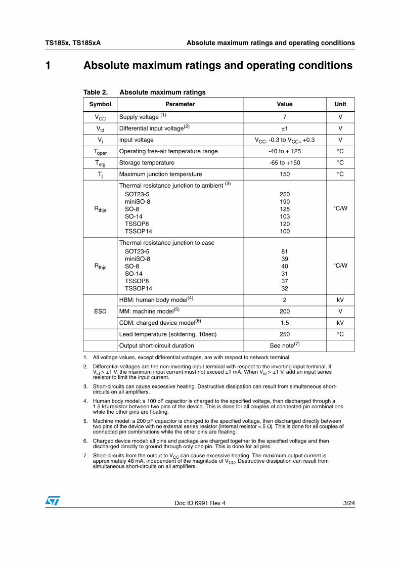
TS185x, TS185xA Absolute maximum ratings and operating conditions
Doc ID 6991 Rev 4 3/24
1 Absolute maximum ratings and operating conditions
Table 2. Absolute maximum ratings
Symbol Parameter Value Unit
VCC Supply voltage (1)
1. All voltage values, except differential voltages, are with respect to network terminal.
7 V
Vid Differential input voltage(2)
2. Differential voltages are the non-inverting input terminal with respect to the inverting input terminal. If Vid > ±1 V, the maximum input current must not exceed ±1 mA. When Vid > ±1 V, add an input series resistor to limit the input current.
±1 V
Vi Input voltage VCC- -0.3 to VCC+ +0.3 V
Toper Operating free-air temperature range -40 to + 125 °C
Tstg Storage temperature -65 to +150 °C
Tj Maximum junction temperature 150 °C
Rthja
Thermal resistance junction to ambient (3)
SOT23-5miniSO-8SO-8SO-14TSSOP8TSSOP14
3. Short-circuits can cause excessive heating. Destructive dissipation can result from simultaneous short-circuits on all amplifiers.
250190125103120100
°C/W
Rthjc
Thermal resistance junction to case
SOT23-5miniSO-8SO-8SO-14TSSOP8TSSOP14
813940313732
°C/W
ESD
HBM: human body model(4)
4. Human body model: a 100 pF capacitor is charged to the specified voltage, then discharged through a 1.5 kΩ resistor between two pins of the device. This is done for all couples of connected pin combinations while the other pins are floating.
2 kV
MM: machine model(5)
5. Machine model: a 200 pF capacitor is charged to the specified voltage, then discharged directly between two pins of the device with no external series resistor (internal resistor < 5 Ω). This is done for all couples of connected pin combinations while the other pins are floating.
200 V
CDM: charged device model(6)
6. Charged device model: all pins and package are charged together to the specified voltage and then discharged directly to ground through only one pin. This is done for all pins.
1.5 kV
Lead temperature (soldering, 10sec) 250 °C
Output short-circuit duration See note(7)
7. Short-circuits from the output to VCC can cause excessive heating. The maximum output current is approximately 48 mA, independent of the magnitude of VCC. Destructive dissipation can result from simultaneous short-circuits on all amplifiers.
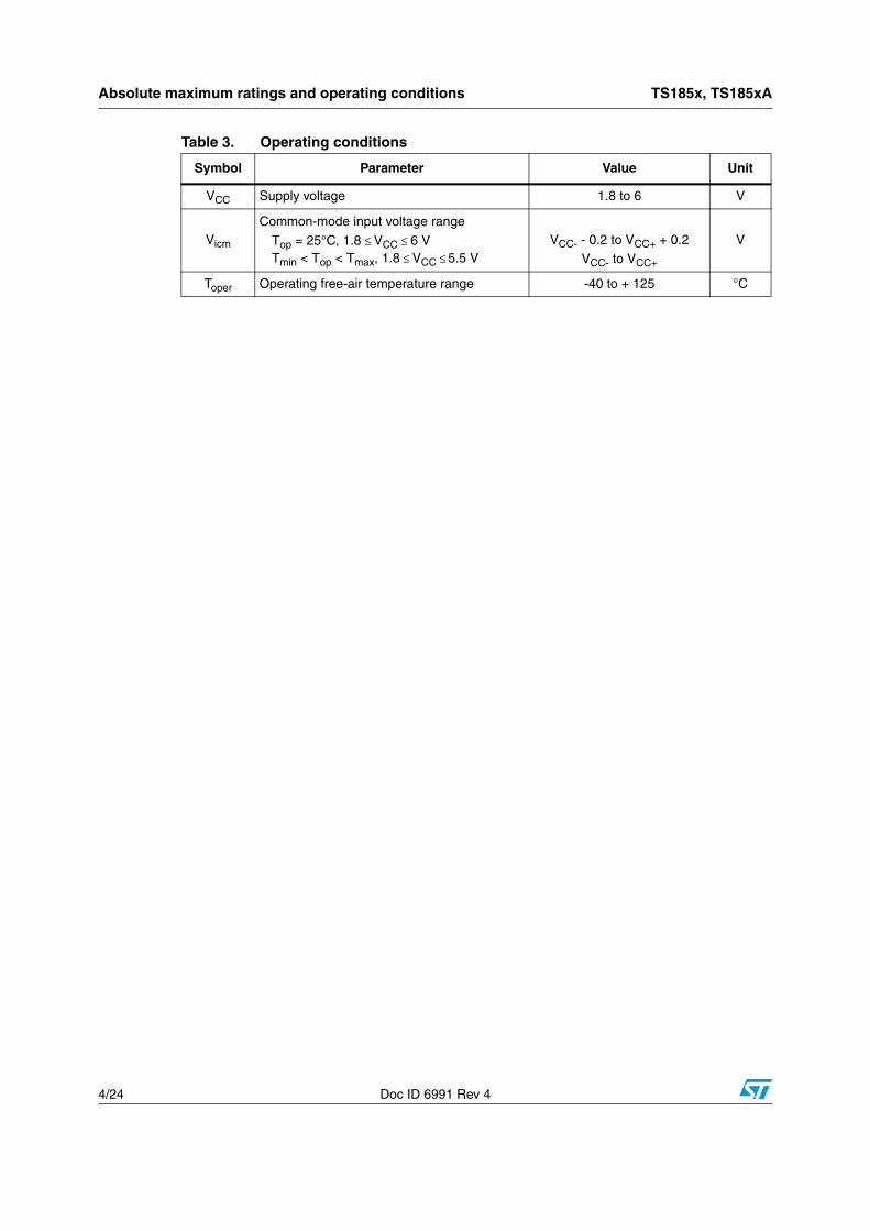
Absolute maximum ratings and operating conditions TS185x, TS185xA
4/24 Doc ID 6991 Rev 4
Table 3. Operating conditions
Symbol Parameter Value Unit
VCC Supply voltage 1.8 to 6 V
Vicm
Common-mode input voltage range
Top = 25°C, 1.8 ≤ VCC ≤ 6 VTmin < Top < Tmax, 1.8 ≤ VCC ≤ 5.5 V
VCC- - 0.2 to VCC+ + 0.2VCC- to VCC+
V
Toper Operating free-air temperature range -40 to + 125 °C

TS185x, TS185xA Electrical characteristics
Doc ID 6991 Rev 4 5/24
2 Electrical characteristics
Table 4. Electrical characteristics measured at VCC+ = +1.8 V, VCC- = 0 V, with CL and RL connected to VCC/2, Tamb = 25°C (unless otherwise specified) (1)
Symbol Parameter Conditions Min. Typ. Max. Unit
Vio Input offset voltage
TS1851/2/4Tmin ≤ Tamb ≤ Tmax
TS1851A/2A/4ATmin ≤ Tamb ≤ Tmax
0.136
11.5
mV
ΔVio Input offset voltage drift 2 μV/°C
Iio Input offset currentVicm = Vout = VCC/2 (2)
Tmin ≤ Tamb ≤ Tmax
1 925
nA
Iib Input bias current Vicm = Vout = VCC/2(2)
Tmin ≤ Tamb ≤ Tmax
10 50
80nA
CMRCommon mode rejection ratio20 log (ΔVic/ΔVio)
0 ≤ Vicm ≤ VCC
Tmin ≤ Tamb ≤ Tmax
5552
85dB
Avd Large signal voltage gainVout = 0.5 to 1.3 V
RL = 10 kΩRL = 2 kΩ
8070
100100
dB
VOH High level output voltage
Vid = 100 mVRL = 10 kΩRL = 2 kΩTmin ≤ Tamb ≤ Tmax, RL = 10 kΩTmin ≤ Tamb ≤ Tmax, RL = 2 kΩ
1.71.651.7
1.65
1.771.7 V
VOL Low level output voltage
Vid = -100 mVRL = 10 kΩRL = 2 kΩTmin ≤ Tamb ≤ Tmax, RL = 10 kΩTmin ≤ Tamb ≤ Tmax, RL = 2 kΩ
4062
7090
100
120
mV
Io
Output source currentVid = 100 mV, VO = VCC-at Tamb 15 29
mAat Tmin ≤ Tamb ≤ Tmax 5 5
Output sink currentVid = -100 mV, VO = VCC+, at Tamb 15 46
mAat Tmin ≤ Tamb ≤ Tmax 5
ICC Supply current (per amplifier)
Vout = VCC/2
AVCL = 1, no load
Tmin ≤ Tamb ≤ Tmax
120 170
200
μA
GBP Gain bandwidth product RL = 10 kΩ, CL = 100 pF, f = 100 kHz 300 530 kHz
SR Slew rate RL = 10 kΩ, CL = 100 pF, AV = 1 0.1 0.18 V/μs
φm Phase margin CL = 100 pF 60 Degrees
en Input voltage noise f = 1 kHz 40 nV/√Hz
THD Total harmonic distortion 0.01 %
1. All parameter limits at temperatures other than 25°C are guaranteed by correlation.
2. Maximum values include unavoidable inaccuracies of the industrial tests.

Electrical characteristics TS185x, TS185xA
6/24 Doc ID 6991 Rev 4
Table 5. Electrical characteristics measured at VCC+ = +3 V, VCC- = 0 V, with CL and RL connected to VCC/2, Tamb = 25°C (unless otherwise specified) (1)
Symbol Parameter Conditions Min. Typ. Max. Unit
Vio Input offset voltage
Vicm = Vout = VCC/2TS1851/2/4Tmin ≤ Tamb ≤ Tmax
TS1851A/2A/4ATmin ≤ Tamb ≤ Tmax
0.1361
1.5
mV
ΔVio Input offset voltage drift 2 μV/°C
Iio Input offset currentVicm = Vout = VCC/2(2)
Tmin ≤ Tamb ≤ Tmax
1 9
25nA
Iib Input bias current Vicm = Vout = VCC/2(2)
Tmin ≤ Tamb ≤ Tmax
10 55
85nA
CMRCommon mode rejection ratio
20 log (ΔVic/ΔVio)
0 ≤ Vicm ≤ VCC
Tmin ≤ Tamb ≤ Tmax
60
57
90dB
Avd Large signal voltage gainVout = 0.5 to 2.5 VRL = 10 kΩRL = 2 kΩ
8374
102102
dB
VOH High level output voltage
Vid = 100 mV
RL = 10 kΩRL = 2 kΩTmin ≤ Tamb ≤ Tmax, RL = 10 kΩTmin ≤ Tamb ≤ Tmax, RL = 2 kΩ
2.92.85
2.92.85
2.962.94 V
VOL Low level output voltage
Vid = -100 mVRL = 10 kΩRL = 2 kΩTmin ≤ Tamb ≤ Tmax, RL = 10 kΩTmin ≤ Tamb ≤ Tmax, RL = 2 kΩ
1046
90100120
130
mV
Io
Output source currentVid = 100 mV, VO = VCC-, at Tamb 15 47
mAAt Tmin ≤ Tamb ≤ Tmax 5
Output sink currentVid = -100 mV, VO = VCC+, at Tamb 15 47
mAAt Tmin ≤ Tamb ≤ Tmax 5
ICC Supply current (per amplifier)Vout = VCC/2AVCL = 1, no load
Tmin ≤ Tamb ≤ Tmax
150 200
230
μA
GBP Gain bandwidth product RL = 10 kΩ, CL = 100 pF, f = 100 kHz 370 600 kHz
SR Slew rate RL = 10 kΩ, CL = 100 pF, AV = 1 0.12 0.2 V/μs
φm Phase margin CL = 100 pF 60 Degrees
en Input voltage noise f = 1 kHz 40 nV/√Hz
THD Total harmonic distortion Vout = 2 Vpk-pk, AV = -1, f = 1 kHz 0.005 %
1. All parameter limits at temperatures other than 25°C are guaranteed by correlation.
2. Maximum values include unavoidable inaccuracies of the industrial tests.
TS185x, TS185xA Electrical characteristics
Doc ID 6991 Rev 4 7/24
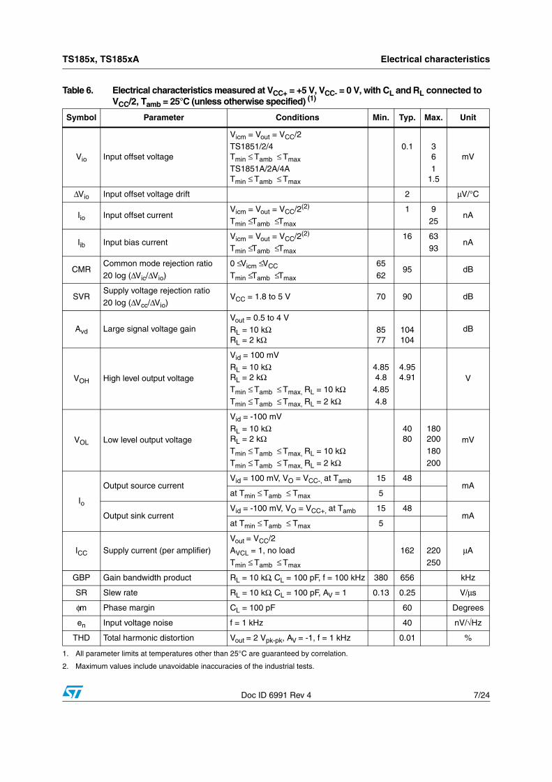
Table 6. Electrical characteristics measured at VCC+ = +5 V, VCC- = 0 V, with CL and RL connected to VCC/2, Tamb = 25°C (unless otherwise specified) (1)
Symbol Parameter Conditions Min. Typ. Max. Unit
Vio Input offset voltage
Vicm = Vout = VCC/2TS1851/2/4Tmin ≤ Tamb ≤ Tmax
TS1851A/2A/4ATmin ≤ Tamb ≤ Tmax
0.1 361
1.5
mV
ΔVio Input offset voltage drift 2 μV/°C
Iio Input offset currentVicm = Vout = VCC/2(2)
Tmin ≤ Tamb ≤ Tmax
1 925
nA
Iib Input bias current Vicm = Vout = VCC/2(2)
Tmin ≤ Tamb ≤ Tmax
16 63
93nA
CMRCommon mode rejection ratio
20 log (ΔVic/ΔVio)
0 ≤ Vicm ≤ VCC
Tmin ≤ Tamb ≤ Tmax
65
6295 dB
SVRSupply voltage rejection ratio
20 log (ΔVcc/ΔVio)VCC = 1.8 to 5 V 70 90 dB
Avd Large signal voltage gainVout = 0.5 to 4 VRL = 10 kΩRL = 2 kΩ
8577
104104
dB
VOH High level output voltage
Vid = 100 mVRL = 10 kΩRL = 2 kΩTmin ≤ Tamb ≤ Tmax, RL = 10 kΩTmin ≤ Tamb ≤ Tmax, RL = 2 kΩ
4.854.8
4.85
4.8
4.954.91 V
VOL Low level output voltage
Vid = -100 mV
RL = 10 kΩRL = 2 kΩTmin ≤ Tamb ≤ Tmax, RL = 10 kΩTmin ≤ Tamb ≤ Tmax, RL = 2 kΩ
4080
180200
180200
mV
Io
Output source currentVid = 100 mV, VO = VCC-, at Tamb 15 48
mAat Tmin ≤ Tamb ≤ Tmax 5
Output sink currentVid = -100 mV, VO = VCC+, at Tamb 15 48
mAat Tmin ≤ Tamb ≤ Tmax 5
ICC Supply current (per amplifier)
Vout = VCC/2
AVCL = 1, no load
Tmin ≤ Tamb ≤ Tmax
162 220
250
μA
GBP Gain bandwidth product RL = 10 kΩ, CL = 100 pF, f = 100 kHz 380 656 kHz
SR Slew rate RL = 10 kΩ, CL = 100 pF, AV = 1 0.13 0.25 V/μs
φm Phase margin CL = 100 pF 60 Degrees
en Input voltage noise f = 1 kHz 40 nV/√Hz
THD Total harmonic distortion Vout = 2 Vpk-pk, AV = -1, f = 1 kHz 0.01 %
1. All parameter limits at temperatures other than 25°C are guaranteed by correlation.
2. Maximum values include unavoidable inaccuracies of the industrial tests.

Electrical characteristics TS185x, TS185xA
8/24 Doc ID 6991 Rev 4
Figure 1. Input offset voltage distribution Figure 2. Input offset voltage vs. temperature
-2. -1.6 -1.2 -.8 -.4 0 .4 .8 1.2 1.6 2
Input Offset Voltage (mV)
0
20
40
60
80
100
Qu
anti
ty o
f P
iece
s
488 pieces testedVcc = 10VTemp = +25°C
-40 -20 0 20 40 60 80 100 120 140Temperature (°C)
-400
-300
-200
-100
0
100
200
300
400
Inp
ut
Vo
ltag
e D
rift
(µ
V)
Vcc = 10V
Vcc = 1.8V
Figure 3. Input bias current vs. temperatureat Vcc = 1.8 V
Figure 4. Input bias current vs. temperatureat Vcc = 3 V
-40 -20 0 20 40 60 80 100 120 140Temperature (°C)
-12
-10
-8
-6
-4
-2
0
Inp
ut
bia
s cu
rren
t (n
A)
Vcc = 1.8VVicm = 0.9V
-40 -20 0 20 40 60 80 100 120 140
Temperature (°C)
-12
-10
-8
-6
-4
-2
0
Inp
ut
bia
s cu
rren
t (n
A) Vcc = 3V
Vicm = 1.5V
Figure 5. Input bias current vs. temperatureat Vcc = 5 V
Figure 6. Supply current/amplifier vs. supply voltage
-40 -20 0 20 40 60 80 100 120 140
Temperature (°C)
-12
-10
-8
-6
-4
-2
0
Inp
ut
bia
s cu
rren
t (n
A) Vcc = 5V
Vicm = 2.5V
0 2 4 6 8
Supply Voltage (V)
0
50
100
150
200
Su
pp
ly C
urr
ent
(µA
)
Tamb = 25°C

TS185x, TS185xA Electrical characteristics
Doc ID 6991 Rev 4 9/24
Figure 7. Supply current/amplifier vs. temperature
Figure 8. Common mode rejection vs. temperature at Vcc = 1.8 V
-40 -20 0 20 40 60 80 100 120 140
Temperature (°C)
90
100
110
120
130
140
150
160
170
Su
pp
ly C
urr
ent
(µA
)
Vcc = 1.8V
Vcc = 5V
Vcc = 3V
j p
-40 -20 0 20 40 60 80 100 120 140Temperature (°C)
60
70
80
90
100
110
Co
mm
on
Mo
de
Rej
ecti
on
(d
B)
Vcc = 1.8V
Figure 9. Common mode rejection vs. temperature at Vcc = 3 V
Figure 10. Common mode rejection vs. temperature at Vcc = 5 Vj p
-50 0 50 100 150
Temperature (°C)
60
70
80
90
100
110
Co
mm
on
Mo
de
Rej
ecti
on
(d
B)
Vcc = 3V
-40-20
020
4060
80100
120140
Temperature (°C)
60
70
80
90
100
110
Com
mon
Mod
e R
ejec
tion
(dB
)
Vcc = 5V
Figure 11. Supply voltage rejection vs. temperature at Vcc = 2 V
Figure 12. Supply voltage rejection vs. temperature at Vcc = 3 V
-40 -20 0 20 40 60 80 100 120 140Temperature (°C)
60
70
80
90
100
110
Su
pp
ly V
olt
age
Rej
ecti
on
(d
B)
Vcc = 2VVicm = 1V
-40-20
020
4060
80100
120140
Temperature (°C)
60
70
80
90
100
110
Supp
ly V
olta
ge R
ejec
tion
(dB
)
Vcc = 3VVicm = 1.5V

Electrical characteristics TS185x, TS185xA
10/24 Doc ID 6991 Rev 4
Figure 13. Supply voltage rejection vs. temperature at Vcc = 5 V
Figure 14. Open loop gain vs. temperatureat Vcc = 1.8 V
-40-20
020
4060
80100
120140
Temperature (°C)
60
70
80
90
100
110
Supp
ly V
olta
ge R
ejec
tion
(dB
) Vcc = 5VVicm = 2.5V
-40-20
020
4060
80100
120140
Temperature (°C)
70
80
90
100
110
Ope
n Lo
op G
ain
(dB
)
Vcc = 1.8V
RL = 10 kohms
RL = 2 kohms
Figure 15. Open loop gain vs. temperatureat Vcc = 3 V
Figure 16. Open loop gain vs. temperatureat Vcc = 5 V
-40-20
020
4060
80100
120140
Temperature (°C)
70
80
90
100
110
Ope
n Lo
op G
ain
(dB
)
Vcc = 3V
RL = 10 kohms
RL = 2 kohms
-40-20
020
4060
80100
120140
Temperature (°C)
70
80
90
100
110O
pen
Loop
Gai
n (d
B)
VCC = 5V RL = 10 kohms
RL = 2 kohms
Figure 17. High level output voltage vs. temperature, RL = 10 kΩ
Figure 18. Low level output voltage vs. temperature, RL = 10 kΩ
-40-20
020
4060
80100
120140
Temperature (°C)
20
25
30
35
40
45
50
55
Volta
ge R
efer
ence
d to
VC
C (m
V)
Vcc = 1.8V
Vcc = 3V
Vcc = 5V
RL = 10 kohms
-40-20
020
4060
80100
120140
Temperature (°C)
20
25
30
35
40
45
50
55
Volta
ge R
efer
ence
d to
Gnd
(mV)
Vcc = 1.8V
Vcc = 3V
Vcc = 5VRL = 10 kohms

TS185x, TS185xA Electrical characteristics
Doc ID 6991 Rev 4 11/24
Figure 19. High level output voltage vs. temperature, RL = 2 kΩ
Figure 20. Low level output voltage vs. temperature, RL = 2 kΩ
-40-20
020
4060
80100
120140
Temperature (°C)
40
50
60
70
80
90
100
110
Volta
ge R
efer
ence
d to
VC
C (m
V)
Vcc = 1.8V
Vcc = 3V
Vcc = 5VRL = 2 kohms
-40-20
020
4060
80100
120140
Temperature (°C)
40
50
60
70
80
90
100
110
Volta
ge R
efer
ence
d to
Gnd
(mV)
Vcc = 1.8V
Vcc = 3V
Vcc = 5VRL = 2 kohms
Figure 21. Output current vs. temperature Figure 22. Output current vs. output voltageat Vcc = 1.8 V
-40-20
020
4060
80100
120140
Temperature (°C)
-60
-40
-20
0
20
40
60
80
Out
put C
urre
nt (m
A)
Isink, Vcc = 1.8V
Vid = 1VIsource, Vcc = 1.8V
Isink, Vcc = 3V
Isink, Vcc = 5V
Isource, Vcc = 3V
Isource, Vcc = 5V
0.00.5
1.01.5
2.0
Output Voltage (V)
-40
-30
-20
-10
0
10
20
30
40
50
60O
utpu
t Cur
rent
(mA
)
sink
Vcc = 1.8V Vid = 0.1V Vicm = 0.9V
source
T = 25 °C
T = -40 °C
T = 125 °C
T = 125 °C
T = -40 °C
T = 25 °C
Figure 23. Output current vs. output voltageat Vcc = 3 V
Figure 24. Output current vs. output voltageat Vcc = 5 V
0.00.5
1.01.5
2.02.5
3.0
Output Voltage (V)
-60
-40
-20
0
20
40
60
80
Out
put C
urre
nt (m
A)
sink
Vcc = 3V Vid = 0.1VVicm = 1.5V
source
T = 25 °CT = -40 °C
T = 125 °C
T = 125 °C
T = -40 °C
T = 25 °C
0.01.0
2.03.0
4.05.0
Output Voltage (V)
-60
-40
-20
0
20
40
60
80
Out
put C
urre
nt (m
A)
sink
Vcc = 5V Vid = 0.1VVicm = 2.5V
source
T = 25 °C
T = -40 °C
T = 125 °C
T = 125 °C
T = -40 °C
T = 25 °C
Electrical characteristics TS185x, TS185xA
12/24 Doc ID 6991 Rev 4
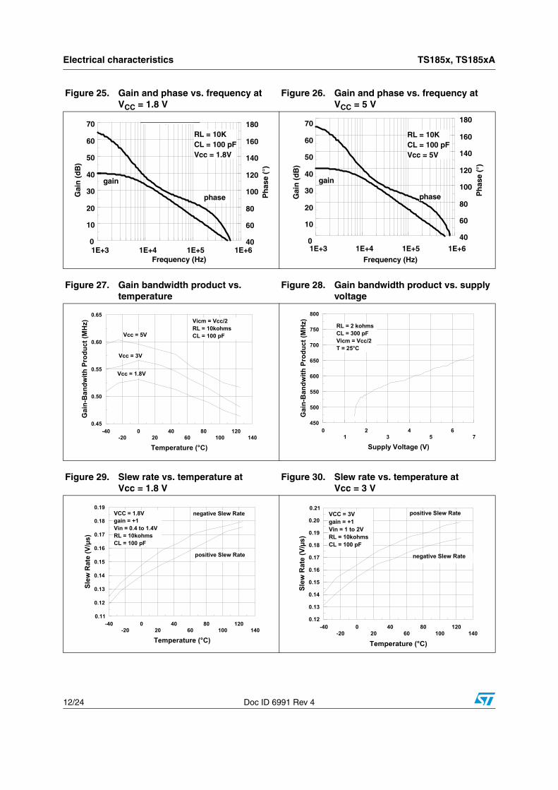
Figure 25. Gain and phase vs. frequency at VCC = 1.8 V
Figure 26. Gain and phase vs. frequency at VCC = 5 V
Frequency
1E+3 1E+4 1E+5 1E+6Frequency (Hz)
0
10
20
30
40
50
60
70
Gai
n (
dB
)
40
60
80
100
120
140
160
180
Ph
ase
(°)
RL = 10KCL = 100 pFVcc = 1.8V
gain
phase
1E+3 1E+4 1E+5 1E+6Frequency (Hz)
0
10
20
30
40
50
60
70
Gai
n (
dB
)
40
60
80
100
120
140
160
180
Ph
ase
(°)
RL = 10KCL = 100 pFVcc = 5V
gain
phase
Figure 27. Gain bandwidth product vs. temperature
Figure 28. Gain bandwidth product vs. supply voltage
-40-20
020
4060
80100
120140
Temperature (°C)
0.45
0.50
0.55
0.60
0.65
Gai
n-B
andw
ith P
rodu
ct (M
Hz)
Vcc = 1.8V
Vcc = 3V
Vcc = 5V
Vicm = Vcc/2RL = 10kohmsCL = 100 pF
01
23
45
67
Supply Voltage (V)
450
500
550
600
650
700
750
800
Gai
n-B
andw
ith P
rodu
ct (M
Hz) RL = 2 kohms
CL = 300 pFVicm = Vcc/2T = 25°C
Figure 29. Slew rate vs. temperature atVcc = 1.8 V
Figure 30. Slew rate vs. temperature at Vcc = 3 V
-40-20
020
4060
80100
120140
Temperature (°C)
0.11
0.12
0.13
0.14
0.15
0.16
0.17
0.18
0.19
Slew
Rat
e (V
/µs)
positive Slew Rate
VCC = 1.8Vgain = +1Vin = 0.4 to 1.4VRL = 10kohmsCL = 100 pF
negative Slew Rate
-40-20
020
4060
80100
120140
Temperature (°C)
0.12
0.13
0.14
0.15
0.16
0.17
0.18
0.19
0.20
0.21
Slew
Rat
e (V
/µs)
positive Slew RateVCC = 3Vgain = +1Vin = 1 to 2VRL = 10kohmsCL = 100 pF
negative Slew Rate

TS185x, TS185xA Electrical characteristics
Doc ID 6991 Rev 4 13/24
Figure 31. Slew rate vs. temperature at Vcc = 5 V
Figure 32. Phase margin vs. load capacitor
-40-20
020
4060
80100
120140
Temperature (°C)
0.13
0.14
0.15
0.16
0.17
0.18
0.19
0.20
0.21
0.22
Slew
Rat
e (V
/µs)
positive Slew RateVCC = 5Vgain = +1Vin = 2 to 3VRL = 10kohmsCL = 100 pF
negative Slew Rate
10100
100010000
Load Capacitor (pF)
-10
0
10
20
30
40
50
60
70
Phas
e M
argi
n (°
)
VCC = 3Vgain = -1
Figure 33. Phase margin vs. output current Figure 34. Equivalent input noise vs. frequency
-10-5
05
10
DC Output Current (mA)
55
60
65
70
75
80
85
Phas
e M
argi
n (°
)
VCC = 3VRL = 2 kohmsCL = 100 pF
1E+11E+2
1E+31E+4
1E+5
Frequency (Hz)
0
10
20
30
40
50
Equi
vale
nt In
put N
oise
(nV/
sqr(
Hz)
)
VCC = 1.8Vgain = 100Rs = 100 ohms
Figure 35. Distortion vs. output voltage atVcc = 1.8 V
Figure 36. Distortion vs. output voltage atVcc = 3 V
0.0000.100
0.2000.300
0.4000.500
0.6000.700
0.800
Output Voltage (V)
0.001
0.010
0.100
1.000
10.000
Dis
tort
ion
(%)
RL = 10kohms
VCC = 1.8Vf = 1kHzT = 25°Cgain = -1
RL = 2kohms
0.0000.200
0.4000.600
0.8001.000
1.200
Output Voltage (V)
0.001
0.010
0.100
1.000
10.000
Dis
tort
ion
(%)
VCC = 3Vf = 1kHzRL = 10KT = 25°Cgain = -1
Electrical characteristics TS185x, TS185xA
14/24 Doc ID 6991 Rev 4
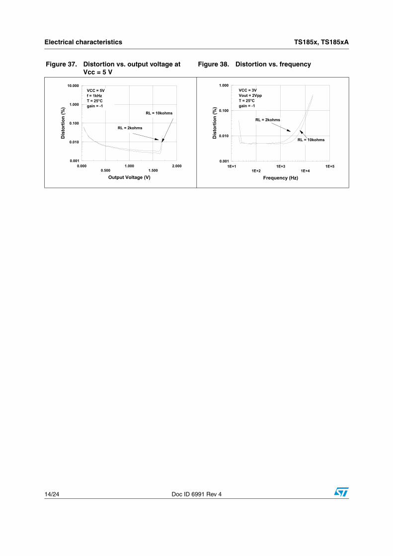
Figure 37. Distortion vs. output voltage atVcc = 5 V
Figure 38. Distortion vs. frequency
0.0000.500
1.0001.500
2.000
Output Voltage (V)
0.001
0.010
0.100
1.000
10.000
Dis
tort
ion
(%)
RL = 10kohms
VCC = 5Vf = 1kHzT = 25°Cgain = -1
RL = 2kohms
1E+11E+2
1E+31E+4
1E+5
Frequency (Hz)
0.001
0.010
0.100
1.000
Dis
tort
ion
(%)
RL = 10kohms
VCC = 3VVout = 2VppT = 25°Cgain = -1
RL = 2kohms
TS185x, TS185xA Package information
Doc ID 6991 Rev 4 15/24
3 Package information
In order to meet environmental requirements, ST offers these devices in different grades of ECOPACK® packages, depending on their level of environmental compliance. ECOPACK® specifications, grade definitions and product status are available at: www.st.com. ECOPACK® is an ST trademark.

Package information TS185x, TS185xA
16/24 Doc ID 6991 Rev 4
3.1 SO-8 package information
Figure 39. SO-8 package mechanical drawing
Table 7. SO-8 package mechanical data
Ref.
Dimensions
Millimeters Inches
Min. Typ. Max. Min. Typ. Max.
A 1.75 0.069
A1 0.10 0.25 0.004 0.010
A2 1.25 0.049
b 0.28 0.48 0.011 0.019
c 0.17 0.23 0.007 0.010
D 4.80 4.90 5.00 0.189 0.193 0.197
E 5.80 6.00 6.20 0.228 0.236 0.244
E1 3.80 3.90 4.00 0.150 0.154 0.157
e 1.27 0.050
h 0.25 0.50 0.010 0.020
L 0.40 1.27 0.016 0.050
L1 1.04 0.040
k 1° 8° 1° 8°
ccc 0.10 0.004
TS185x, TS185xA Package information
Doc ID 6991 Rev 4 17/24
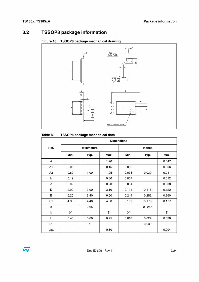
3.2 TSSOP8 package information
Figure 40. TSSOP8 package mechanical drawing
Table 8. TSSOP8 package mechanical data
Ref.
Dimensions
Millimeters Inches
Min. Typ. Max. Min. Typ. Max.
A 1.20 0.047
A1 0.05 0.15 0.002 0.006
A2 0.80 1.00 1.05 0.031 0.039 0.041
b 0.19 0.30 0.007 0.012
c 0.09 0.20 0.004 0.008
D 2.90 3.00 3.10 0.114 0.118 0.122
E 6.20 6.40 6.60 0.244 0.252 0.260
E1 4.30 4.40 4.50 0.169 0.173 0.177
e 0.65 0.0256
k 0° 8° 0° 8°
L 0.45 0.60 0.75 0.018 0.024 0.030
L1 1 0.039
aaa 0.10 0.004

Package information TS185x, TS185xA
18/24 Doc ID 6991 Rev 4
3.3 MiniSO-8 package information
Figure 41. MiniSO-8 package mechanical drawing
Table 9. MiniSO-8 package mechanical data
Ref.
Dimensions
Millimeters Inches
Min. Typ. Max. Min. Typ. Max.
A 1.1 0.043
A1 0 0.15 0 0.006
A2 0.75 0.85 0.95 0.030 0.033 0.037
b 0.22 0.40 0.009 0.016
c 0.08 0.23 0.003 0.009
D 2.80 3.00 3.20 0.11 0.118 0.126
E 4.65 4.90 5.15 0.183 0.193 0.203
E1 2.80 3.00 3.10 0.11 0.118 0.122
e 0.65 0.026
L 0.40 0.60 0.80 0.016 0.024 0.031
L1 0.95 0.037
L2 0.25 0.010
k 0° 8° 0° 8°
ccc 0.10 0.004

TS185x, TS185xA Package information
Doc ID 6991 Rev 4 19/24
3.4 SO-14 package information
Figure 42. SO-14 package mechanical drawing
Table 10. SO-14 package mechanical data
Dimensions
Ref.Millimeters Inches
Min. Typ. Max. Min. Typ. Max.
A 1.35 1.75 0.05 0.068
A1 0.10 0.25 0.004 0.009
A2 1.10 1.65 0.04 0.06
B 0.33 0.51 0.01 0.02
C 0.19 0.25 0.007 0.009
D 8.55 8.75 0.33 0.34
E 3.80 4.0 0.15 0.15
e 1.27 0.05
H 5.80 6.20 0.22 0.24
h 0.25 0.50 0.009 0.02
L 0.40 1.27 0.015 0.05
k 8° (max.)
ddd 0.10 0.004

Package information TS185x, TS185xA
20/24 Doc ID 6991 Rev 4
3.5 TSSOP14 package information
Figure 43. TSSOP14 package mechanical drawing
Table 11. TSSOP14 package mechanical data
Ref.
Dimensions
Millimeters Inches
Min. Typ. Max. Min. Typ. Max.
A 1.20 0.047
A1 0.05 0.15 0.002 0.004 0.006
A2 0.80 1.00 1.05 0.031 0.039 0.041
b 0.19 0.30 0.007 0.012
c 0.09 0.20 0.004 0.0089
D 4.90 5.00 5.10 0.193 0.197 0.201
E 6.20 6.40 6.60 0.244 0.252 0.260
E1 4.30 4.40 4.50 0.169 0.173 0.176
e 0.65 0.0256
L 0.45 0.60 0.75 0.018 0.024 0.030
L1 1.00 0.039
k 0° 8° 0° 8°
aaa 0.10 0.004

TS185x, TS185xA Package information
Doc ID 6991 Rev 4 21/24
3.6 SOT23-5 package information
Figure 44. SOT23-5L package mechanical drawing
Table 12. SOT23-5L package mechanical data
Ref.
Dimensions
Millimeters Inches
Min. Typ. Max. Min. Typ. Max.
A 0.90 1.20 1.45 0.035 0.047 0.057
A1 0.15 0.006
A2 0.90 1.05 1.30 0.035 0.041 0.051
B 0.35 0.40 0.50 0.013 0.015 0.019
C 0.09 0.15 0.20 0.003 0.006 0.008
D 2.80 2.90 3.00 0.110 0.114 0.118
D1 1.90 0.075
e 0.95 0.037
E 2.60 2.80 3.00 0.102 0.110 0.118
F 1.50 1.60 1.75 0.059 0.063 0.069
L 0.10 0.35 0.60 0.004 0.013 0.023
K 0° 10°
Ordering information TS185x, TS185xA
22/24 Doc ID 6991 Rev 4
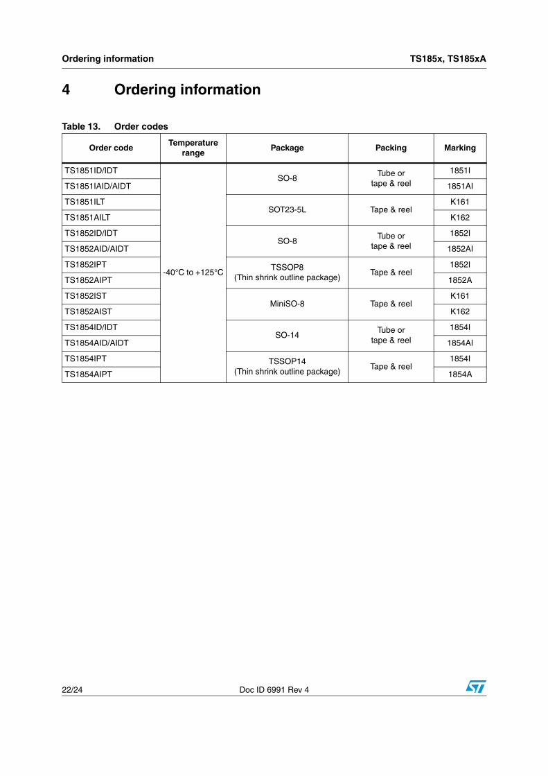
4 Ordering information
Table 13. Order codes
Order codeTemperature
rangePackage Packing Marking
TS1851ID/IDT
-40°C to +125°C
SO-8Tube or
tape & reel
1851I
TS1851IAID/AIDT 1851AI
TS1851ILTSOT23-5L Tape & reel
K161
TS1851AILT K162
TS1852ID/IDTSO-8
Tube ortape & reel
1852I
TS1852AID/AIDT 1852AI
TS1852IPT TSSOP8(Thin shrink outline package)
Tape & reel1852I
TS1852AIPT 1852A
TS1852ISTMiniSO-8 Tape & reel
K161
TS1852AIST K162
TS1854ID/IDTSO-14
Tube ortape & reel
1854I
TS1854AID/AIDT 1854AI
TS1854IPT TSSOP14(Thin shrink outline package)
Tape & reel1854I
TS1854AIPT 1854A
TS185x, TS185xA Revision history
Doc ID 6991 Rev 4 23/24
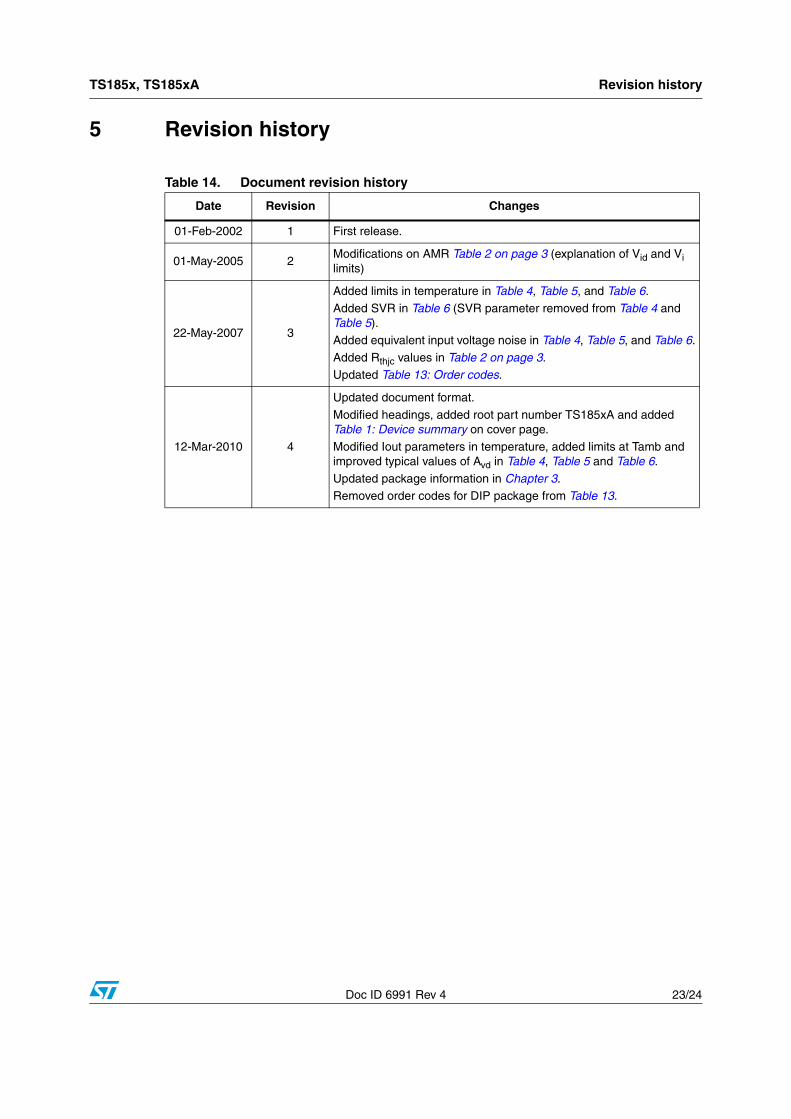
5 Revision history
Table 14. Document revision history
Date Revision Changes
01-Feb-2002 1 First release.
01-May-2005 2Modifications on AMR Table 2 on page 3 (explanation of Vid and Vi limits)
22-May-2007 3
Added limits in temperature in Table 4, Table 5, and Table 6.
Added SVR in Table 6 (SVR parameter removed from Table 4 and Table 5).
Added equivalent input voltage noise in Table 4, Table 5, and Table 6.
Added Rthjc values in Table 2 on page 3.Updated Table 13: Order codes.
12-Mar-2010 4
Updated document format.
Modified headings, added root part number TS185xA and added Table 1: Device summary on cover page.
Modified Iout parameters in temperature, added limits at Tamb and improved typical values of Avd in Table 4, Table 5 and Table 6.
Updated package information in Chapter 3.Removed order codes for DIP package from Table 13.

TS185x, TS185xA
24/24 Doc ID 6991 Rev 4
Please Read Carefully:
Information in this document is provided solely in connection with ST products. STMicroelectronics NV and its subsidiaries (“ST”) reserve theright to make changes, corrections, modifications or improvements, to this document, and the products and services described herein at anytime, without notice.
All ST products are sold pursuant to ST’s terms and conditions of sale.
Purchasers are solely responsible for the choice, selection and use of the ST products and services described herein, and ST assumes noliability whatsoever relating to the choice, selection or use of the ST products and services described herein.
No license, express or implied, by estoppel or otherwise, to any intellectual property rights is granted under this document. If any part of thisdocument refers to any third party products or services it shall not be deemed a license grant by ST for the use of such third party productsor services, or any intellectual property contained therein or considered as a warranty covering the use in any manner whatsoever of suchthird party products or services or any intellectual property contained therein.
UNLESS OTHERWISE SET FORTH IN ST’S TERMS AND CONDITIONS OF SALE ST DISCLAIMS ANY EXPRESS OR IMPLIEDWARRANTY WITH RESPECT TO THE USE AND/OR SALE OF ST PRODUCTS INCLUDING WITHOUT LIMITATION IMPLIEDWARRANTIES OF MERCHANTABILITY, FITNESS FOR A PARTICULAR PURPOSE (AND THEIR EQUIVALENTS UNDER THE LAWSOF ANY JURISDICTION), OR INFRINGEMENT OF ANY PATENT, COPYRIGHT OR OTHER INTELLECTUAL PROPERTY RIGHT.
UNLESS EXPRESSLY APPROVED IN WRITING BY AN AUTHORIZED ST REPRESENTATIVE, ST PRODUCTS ARE NOTRECOMMENDED, AUTHORIZED OR WARRANTED FOR USE IN MILITARY, AIR CRAFT, SPACE, LIFE SAVING, OR LIFE SUSTAININGAPPLICATIONS, NOR IN PRODUCTS OR SYSTEMS WHERE FAILURE OR MALFUNCTION MAY RESULT IN PERSONAL INJURY,DEATH, OR SEVERE PROPERTY OR ENVIRONMENTAL DAMAGE. ST PRODUCTS WHICH ARE NOT SPECIFIED AS "AUTOMOTIVEGRADE" MAY ONLY BE USED IN AUTOMOTIVE APPLICATIONS AT USER’S OWN RISK.
Resale of ST products with provisions different from the statements and/or technical features set forth in this document shall immediately voidany warranty granted by ST for the ST product or service described herein and shall not create or extend in any manner whatsoever, anyliability of ST.
ST and the ST logo are trademarks or registered trademarks of ST in various countries.
Information in this document supersedes and replaces all information previously supplied.
The ST logo is a registered trademark of STMicroelectronics. All other names are the property of their respective owners.
© 2010 STMicroelectronics - All rights reserved
STMicroelectronics group of companies
Australia - Belgium - Brazil - Canada - China - Czech Republic - Finland - France - Germany - Hong Kong - India - Israel - Italy - Japan - Malaysia - Malta - Morocco - Philippines - Singapore - Spain - Sweden - Switzerland - United Kingdom - United States of America
www.st.com