MC33926, 5.0 A Throttle Control H-Bridge - Data Sheet · applicable to any low-voltage DC servo...
26
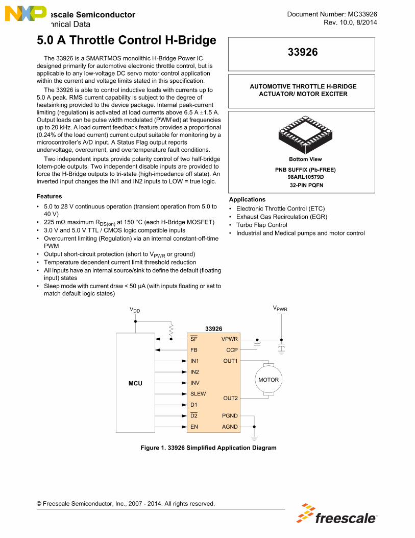
Document Number: MC33926 Rev. 10.0, 8/2014 Freescale Semiconductor Technical Data © Freescale Semiconductor, Inc., 2007 - 2014. All rights reserved. 5.0 A Throttle Control H-Bridge The 33926 is a SMARTMOS monolithic H-Bridge Power IC designed primarily for automotive electronic throttle control, but is applicable to any low-voltage DC servo motor control application within the current and voltage limits stated in this specification. The 33926 is able to control inductive loads with currents up to 5.0 A peak. RMS current capability is subject to the degree of heatsinking provided to the device package. Internal peak-current limiting (regulation) is activated at load currents above 6.5 A 1.5 A. Output loads can be pulse width modulated (PWM’ed) at frequencies up to 20 kHz. A load current feedback feature provides a proportional (0.24% of the load current) current output suitable for monitoring by a microcontroller’s A/D input. A Status Flag output reports undervoltage, overcurrent, and overtemperature fault conditions. Two independent inputs provide polarity control of two half-bridge totem-pole outputs. Two independent disable inputs are provided to force the H-Bridge outputs to tri-state (high-impedance off state). An inverted input changes the IN1 and IN2 inputs to LOW = true logic. Features • 5.0 to 28 V continuous operation (transient operation from 5.0 to 40 V) • 225 m maximum R DS(on) at 150 °C (each H-Bridge MOSFET) • 3.0 V and 5.0 V TTL / CMOS logic compatible inputs • Overcurrent limiting (Regulation) via an internal constant-off-time PWM • Output short-circuit protection (short to V PWR or ground) • Temperature dependent current limit threshold reduction • All Inputs have an internal source/sink to define the default (floating input) states • Sleep mode with current draw < 50 μA (with inputs floating or set to match default logic states) Figure 1. 33926 Simplified Application Diagram PNB SUFFIX (Pb-FREE) 32-PIN PQFN Bottom View 33926 AUTOMOTIVE THROTTLE H-BRIDGE ACTUATOR/ MOTOR EXCITER 98ARL10579D Applications • Electronic Throttle Control (ETC) • Exhaust Gas Recirculation (EGR) • Turbo Flap Control • Industrial and Medical pumps and motor control SF FB IN1 IN2 INV SLEW D1 D2 EN VPWR CCP OUT1 OUT2 PGND AGND MCU 33926 V PWR V DD MOTOR
Transcript of MC33926, 5.0 A Throttle Control H-Bridge - Data Sheet · applicable to any low-voltage DC servo...
Document Number: MC33926Rev. 10.0, 8/2014
Freescale SemiconductorTechnical Data
5.0 A Throttle Control H-BridgeThe 33926 is a SMARTMOS monolithic H-Bridge Power IC
designed primarily for automotive electronic throttle control, but is applicable to any low-voltage DC servo motor control application within the current and voltage limits stated in this specification.
The 33926 is able to control inductive loads with currents up to 5.0 A peak. RMS current capability is subject to the degree of heatsinking provided to the device package. Internal peak-current limiting (regulation) is activated at load currents above 6.5 A 1.5 A. Output loads can be pulse width modulated (PWM’ed) at frequencies up to 20 kHz. A load current feedback feature provides a proportional (0.24% of the load current) current output suitable for monitoring by a microcontroller’s A/D input. A Status Flag output reports undervoltage, overcurrent, and overtemperature fault conditions.
Two independent inputs provide polarity control of two half-bridge totem-pole outputs. Two independent disable inputs are provided to force the H-Bridge outputs to tri-state (high-impedance off state). An inverted input changes the IN1 and IN2 inputs to LOW = true logic.
Features
• 5.0 to 28 V continuous operation (transient operation from 5.0 to 40 V)
• 225 m maximum RDS(on) at 150 °C (each H-Bridge MOSFET)• 3.0 V and 5.0 V TTL / CMOS logic compatible inputs• Overcurrent limiting (Regulation) via an internal constant-off-time
PWM• Output short-circuit protection (short to VPWR or ground)• Temperature dependent current limit threshold reduction• All Inputs have an internal source/sink to define the default (floating
input) states• Sleep mode with current draw < 50 µA (with inputs floating or set to
match default logic states)
Figure 1. 33926 Simplified Application Diagram
SCALE 2:1
PNB SUFFIX (Pb-FREE)
32-PIN PQFN
Bottom View
33926
AUTOMOTIVE THROTTLE H-BRIDGE ACTUATOR/ MOTOR EXCITER
98ARL10579D
Applications
• Electronic Throttle Control (ETC)• Exhaust Gas Recirculation (EGR)• Turbo Flap Control• Industrial and Medical pumps and motor control
SF
FB
IN1
IN2
INV
SLEW
D1
D2
EN
VPWR
CCP
OUT1
OUT2
PGND
AGND
MCU
33926
VPWRVDD
MOTOR
© Freescale Semiconductor, Inc., 2007 - 2014. All rights reserved.

ORDERABLE PARTS
ORDERABLE PARTS
This section describes the part numbers available to be purchased along with their differences. Valid orderable part numbers are provided on the web. To determine the orderable part numbers for this device, go to http://www.freescale.com and perform a part number search for the following device numbers.
Table 1. Orderable Part Variations
Part Number Notes Temperature (TA) Package
MC33926PNB (1) -40 to 125 °C 32 PQFN
Notes1. To order parts in Tape & Reel, add the R2 suffix to the part number.
Analog Integrated Circuit Device Data2 Freescale Semiconductor
33926

INTERNAL BLOCK DIAGRAM
INTERNAL BLOCK DIAGRAM
Figure 2. 33926 Simplified Internal Block Diagram
VDDLOGIC SUPPLY
CHARGEPUMP
GATE DRIVEAND
PROTECTIONLOGIC
CURRENT MIRRORAND
CONSTANT OFF-TIMEPWM CURRENT REGULATOR
VCPCCP
OUT1
OUT2
PGND
TO GATES
HS1
LS1
HS2
LS2
VPWR
VSENSE
ILIM PWM
HS1 HS2
LS1 LS2LS2EN
IN1
IN2
D2
D1
INV
SLEW
SF
FB
AGND
PGND
Analog Integrated Circuit Device DataFreescale Semiconductor 3
33926
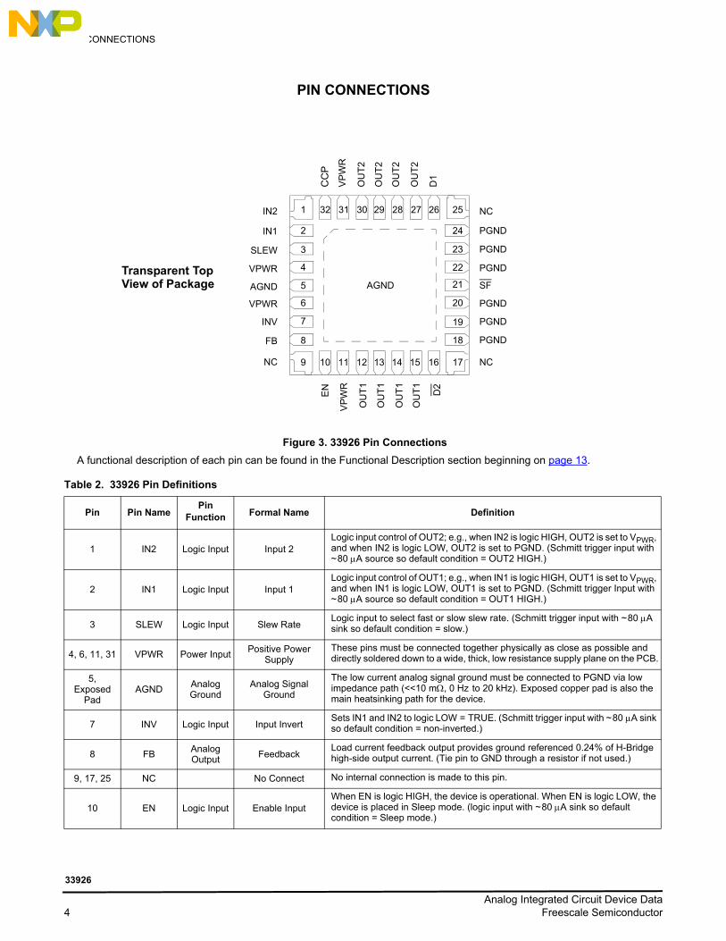
PIN CONNECTIONS
PIN CONNECTIONS
Figure 3. 33926 Pin Connections
A functional description of each pin can be found in the Functional Description section beginning on page 13. Table 2. 33926 Pin Definitions
Pin Pin NamePin
Function Formal Name Definition
1 IN2 Logic Input Input 2Logic input control of OUT2; e.g., when IN2 is logic HIGH, OUT2 is set to VPWR, and when IN2 is logic LOW, OUT2 is set to PGND. (Schmitt trigger input with ~ 80 A source so default condition = OUT2 HIGH.)
2 IN1 Logic Input Input 1Logic input control of OUT1; e.g., when IN1 is logic HIGH, OUT1 is set to VPWR, and when IN1 is logic LOW, OUT1 is set to PGND. (Schmitt trigger Input with ~ 80 A source so default condition = OUT1 HIGH.)
3 SLEW Logic Input Slew RateLogic input to select fast or slow slew rate. (Schmitt trigger input with ~ 80 A sink so default condition = slow.)
4, 6, 11, 31 VPWR Power InputPositive Power
SupplyThese pins must be connected together physically as close as possible and directly soldered down to a wide, thick, low resistance supply plane on the PCB.
5, Exposed
PadAGND
Analog Ground
Analog Signal Ground
The low current analog signal ground must be connected to PGND via low impedance path (<<10 m, 0 Hz to 20 kHz). Exposed copper pad is also the main heatsinking path for the device.
7 INV Logic Input Input InvertSets IN1 and IN2 to logic LOW = TRUE. (Schmitt trigger input with ~ 80 A sink so default condition = non-inverted.)
8 FBAnalog Output
FeedbackLoad current feedback output provides ground referenced 0.24% of H-Bridge high-side output current. (Tie pin to GND through a resistor if not used.)
9, 17, 25 NC No Connect No internal connection is made to this pin.
10 EN Logic Input Enable InputWhen EN is logic HIGH, the device is operational. When EN is logic LOW, the device is placed in Sleep mode. (logic input with ~ 80 A sink so default condition = Sleep mode.)
Transparent Top
25
17
18
19
20
21
22
23
24
9 10 11 12 13 14 15 16
1
2
3
4
5
6
7
8
26272829303132 NC
NC
VP
WR
NC
IN2
IN1
SLEW
OU
T1
AGND
INV
FB
EN
OU
T1
VPWR
VPWR
OU
T2
OU
T2
AGND
OU
T1
D2
PGND
SF
D1
OU
T2
OU
T2
CC
P
VP
WR
PGND
PGND
PGND
PGND
PGND
OU
T1
View of Package
Analog Integrated Circuit Device Data4 Freescale Semiconductor
33926

PIN CONNECTIONS
12, 13,14, 15
OUT1Power Output
H-Bridge Output 1 Source of high-side MOSFET1 and drain of low-side MOSFET1.
16 D2 Logic InputDisable Input 2
(Active Low)When D2 is logic LOW, both OUT1 and OUT2 are tri-stated. (Schmitt trigger input with ~80 A sink so default condition = disabled.)
18 – 20, 22 – 24
PGNDPower Ground
Power GroundHigh-current power ground pins must be connected together physically as close as possible and directly soldered down to a wide, thick, low resistance ground plane on the PCB.
21 SFLogic
Output - Open Drain
Status Flag(Active Low)
Open drain active LOW status flag output (requires an external pull-up resistor to VDD. Maximum permissible load current < 0.5 mA. Maximum VCESAT < 0.4 V at 0.3 mA. Maximum permissible pull-up voltage < 7.0 V.)
26 D1 Logic InputDisable Input 1(Active High)
When D1 is logic HIGH, both OUT1 and OUT2 are tri-stated. Schmitt trigger input with ~80 A source so default condition = disabled.
27, 28,29, 30
OUT2Power Output
H-Bridge Output 2 Source of high-side MOSFET2 and drain of low-side MOSFET2.
32 CCPAnalog Output
Charge Pump Capacitor
External reservoir capacitor connection for internal charge pump; connected to VPWR. Allowable values are 30 to 100 F. Note: This capacitor is required for the proper performance of the device.
Table 2. 33926 Pin Definitions (continued)
Pin Pin NamePin
Function Formal Name Definition
Analog Integrated Circuit Device DataFreescale Semiconductor 5
33926
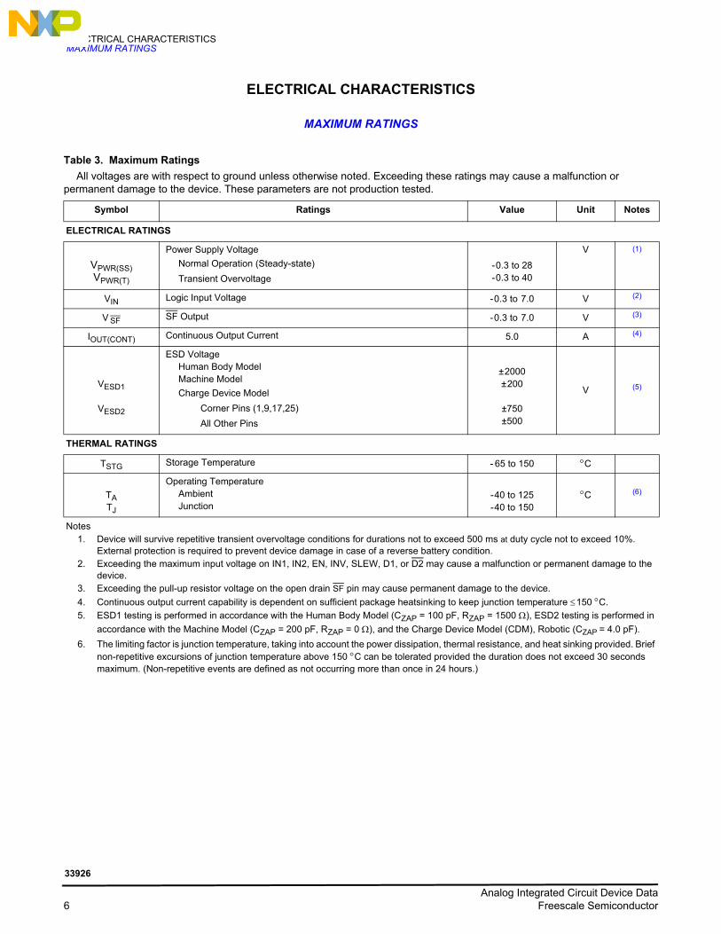
ELECTRICAL CHARACTERISTICSMAXIMUM RATINGS
ELECTRICAL CHARACTERISTICS
MAXIMUM RATINGS
Table 3. Maximum Ratings
All voltages are with respect to ground unless otherwise noted. Exceeding these ratings may cause a malfunction or permanent damage to the device. These parameters are not production tested.
Symbol Ratings Value Unit Notes
ELECTRICAL RATINGS
VPWR(SS)VPWR(T)
Power Supply Voltage
Normal Operation (Steady-state)
Transient Overvoltage
- 0.3 to 28- 0.3 to 40
V (1)
VIN Logic Input Voltage - 0.3 to 7.0 V (2)
V SF SF Output - 0.3 to 7.0 V (3)
IOUT(CONT) Continuous Output Current 5.0 A (4)
VESD1
VESD2
ESD Voltage Human Body Model Machine Model
Charge Device Model
Corner Pins (1,9,17,25)
All Other Pins
± 2000± 200
±750±500
V (5)
THERMAL RATINGS
TSTG Storage Temperature - 65 to 150 C
TATJ
Operating Temperature Ambient Junction
- 40 to 125- 40 to 150
C (6)
Notes1. Device will survive repetitive transient overvoltage conditions for durations not to exceed 500 ms at duty cycle not to exceed 10%.
External protection is required to prevent device damage in case of a reverse battery condition.2. Exceeding the maximum input voltage on IN1, IN2, EN, INV, SLEW, D1, or D2 may cause a malfunction or permanent damage to the
device.3. Exceeding the pull-up resistor voltage on the open drain SF pin may cause permanent damage to the device.
4. Continuous output current capability is dependent on sufficient package heatsinking to keep junction temperature 150 C.
5. ESD1 testing is performed in accordance with the Human Body Model (CZAP = 100 pF, RZAP = 1500 ), ESD2 testing is performed in
accordance with the Machine Model (CZAP = 200 pF, RZAP = 0 ), and the Charge Device Model (CDM), Robotic (CZAP = 4.0 pF).
6. The limiting factor is junction temperature, taking into account the power dissipation, thermal resistance, and heat sinking provided. Brief non-repetitive excursions of junction temperature above 150 C can be tolerated provided the duration does not exceed 30 seconds maximum. (Non-repetitive events are defined as not occurring more than once in 24 hours.)
Analog Integrated Circuit Device Data6 Freescale Semiconductor
33926

ELECTRICAL CHARACTERISTICSMAXIMUM RATINGS
TPPRT Peak Package Reflow Temperature During Reflow 250 °C (7) (8)
RJC Approximate Junction-to-Case Thermal Resistance < 1.0 C/W (9)
Notes7. Pin soldering temperature limit is for 10 seconds maximum duration. Not designed for immersion soldering. Exceeding these limits may
cause malfunction or permanent damage to the device.8. Freescale’s Package Reflow capability meets Pb-free requirements for JEDEC standard J-STD-020C for Peak Package Reflow
Temperature and Moisture Sensitivity Levels (MSL),9. Exposed heatsink pad plus the power and ground pins comprise the main heat conduction paths. The actual RJB (junction-to-PC board)
values will vary depending on solder thickness and composition and copper trace thickness and area. Maximum current at maximum die temperature represents ~16 W of conduction loss heating in the diagonal pair of output MOSFETs. Therefore, the RJA must be < 5.0 C/W for maximum current at 70 C ambient. Module thermal design must be planned accordingly.
Table 3. Maximum Ratings (continued)
All voltages are with respect to ground unless otherwise noted. Exceeding these ratings may cause a malfunction or permanent damage to the device. These parameters are not production tested.
Symbol Ratings Value Unit Notes
Analog Integrated Circuit Device DataFreescale Semiconductor 7
33926
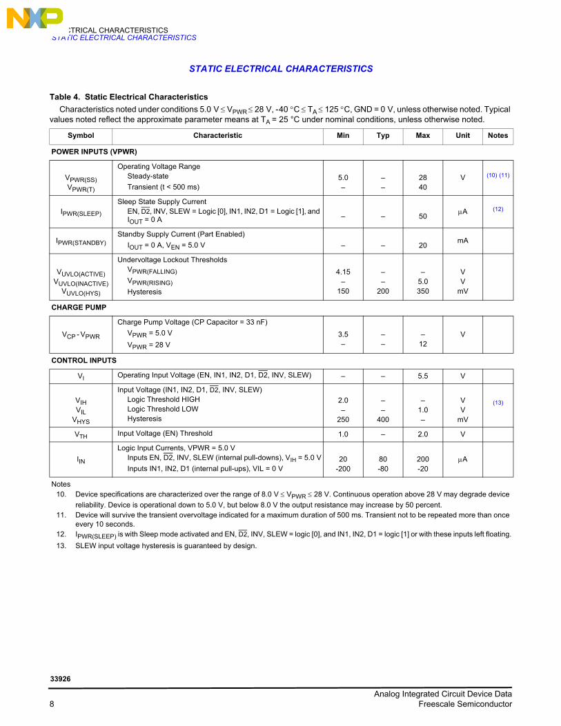
ELECTRICAL CHARACTERISTICSSTATIC ELECTRICAL CHARACTERISTICS
STATIC ELECTRICAL CHARACTERISTICS
Table 4. Static Electrical Characteristics
Characteristics noted under conditions 5.0 V VPWR 28 V, - 40 C TA 125 C, GND = 0 V, unless otherwise noted. Typical values noted reflect the approximate parameter means at TA = 25 °C under nominal conditions, unless otherwise noted.
Symbol Characteristic Min Typ Max Unit Notes
POWER INPUTS (VPWR)
VPWR(SS)VPWR(T)
Operating Voltage Range Steady-state
Transient (t < 500 ms) 5.0–
––
2840
V (10) (11)
IPWR(SLEEP)
Sleep State Supply Current EN, D2, INV, SLEW = Logic [0], IN1, IN2, D1 = Logic [1], and IOUT = 0 A – – 50
A (12)
IPWR(STANDBY)Standby Supply Current (Part Enabled)
IOUT = 0 A, VEN = 5.0 V – – 20mA
VUVLO(ACTIVE)VUVLO(INACTIVE)
VUVLO(HYS)
Undervoltage Lockout ThresholdsVPWR(FALLING)
VPWR(RISING)
Hysteresis
4.15–
150
––
200
–5.0350
VV
mV
CHARGE PUMP
VCP - VPWR
Charge Pump Voltage (CP Capacitor = 33 nF)
VPWR = 5.0 V
VPWR = 28 V
3.5–
––
–12
V
CONTROL INPUTS
VI Operating Input Voltage (EN, IN1, IN2, D1, D2, INV, SLEW) – – 5.5 V
VIHVIL
VHYS
Input Voltage (IN1, IN2, D1, D2, INV, SLEW) Logic Threshold HIGHLogic Threshold LOW Hysteresis
2.0–
250
––
400
–1.0–
VV
mV
(13)
VTH Input Voltage (EN) Threshold 1.0 – 2.0 V
IIN
Logic Input Currents, VPWR = 5.0 VInputs EN, D2, INV, SLEW (internal pull-downs), VIH = 5.0 V
Inputs IN1, IN2, D1 (internal pull-ups), VIL = 0 V20
-20080-80
200-20
A
Notes10. Device specifications are characterized over the range of 8.0 V VPWR 28 V. Continuous operation above 28 V may degrade device
reliability. Device is operational down to 5.0 V, but below 8.0 V the output resistance may increase by 50 percent.11. Device will survive the transient overvoltage indicated for a maximum duration of 500 ms. Transient not to be repeated more than once
every 10 seconds.12. IPWR(SLEEP) is with Sleep mode activated and EN, D2, INV, SLEW = logic [0], and IN1, IN2, D1 = logic [1] or with these inputs left floating.
13. SLEW input voltage hysteresis is guaranteed by design.
Analog Integrated Circuit Device Data8 Freescale Semiconductor
33926

ELECTRICAL CHARACTERISTICSSTATIC ELECTRICAL CHARACTERISTICS
POWER OUTPUTS OUT1, OUT2
RDS(ON)
Output-ON Resistance, ILOAD = 3.0 AVPWR = 8.0 V, TJ = 25 CVPWR = 8.0 V, TJ = 150 CVPWR = 5.0 V, TJ = 150 C
–––
120––
–225325
m (15)
ILIM
Output Current Regulation ThresholdTJ < TFB
TJ TFB (Fold back Region - see Figure 9 and Figure 11) 5.2–
6.54.2
8.0–
A (14)
ISCHHigh-side Short-circuit Detection Threshold (Short-circuit to GND) 11 13 16 A (14)
ISCLLow-side Short-circuit Detection Threshold (Short-circuit to VPWR) 9.0 11 14 A (14)
IOUTLEAK
Output Leakage Current, Outputs off, VPWR = 28 V
VOUT = VPWR
VOUT = Ground
––60
––
100–
A (16)
VF
Output MOSFET Body Diode Forward Voltage DropIOUT = 3.0 A – – 2.0
V
TLIMTHYS
Overtemperature Shutdown Thermal Limit at TJ
Hysteresis at TJ
175–
–12
200–
C (14)
TFB Current Foldback at TJ(14) 165 – 185 C
TSEP Current Foldback to Thermal Shutdown Separation (14) 10 – 15 C
HIGH-SIDE CURRENT SENSE FEEDBACK
I FB
Feedback Current (pin FB sourcing current) (17)
I OUT = 0 mA
I OUT = 300 mA
I OUT = 500 mA
I OUT = 1.5 A
I OUT = 3.0 A
I OUT = 6.0 A
0.00.0
0.352.865.71
11.43
–270
0.7753.577.14
14.29
507501.564.288.57
17.15
AAmAmAmAmA
STATUS FLAG (18)
ISFLEAKStatus Flag Leakage Current
V SF = 5.0 V – – 5.0A (19)
VSFLOWStatus Flag SET Voltage
I SF = 300 µA – – 0.4V (20)
Notes14. This parameter is guaranteed by design.15. Output-ON resistance as measured from output to VPWR and from output to GND.16. Outputs switched OFF via D1 or D2. 17. Accuracy is better than 20% from 0.5 to 6.0 A. Recommended terminating resistor value: RFB = 270
18. Status Flag output is an open drain output requiring a pull-up resistor to logic VDD.
19. Status Flag Leakage Current is measured with Status Flag HIGH and not SET.20. Status Flag Set Voltage measured with Status Flag LOW and SET with I FS = 300 A. Maximum allowable sink current from this pin is
< | 500 A | . Maximum allowable pull-up voltage < 7.0 V.
Table 4. Static Electrical Characteristics (continued)
Characteristics noted under conditions 5.0 V VPWR 28 V, - 40 C TA 125 C, GND = 0 V, unless otherwise noted. Typical values noted reflect the approximate parameter means at TA = 25 °C under nominal conditions, unless otherwise noted.
Symbol Characteristic Min Typ Max Unit Notes
Analog Integrated Circuit Device DataFreescale Semiconductor 9
33926

ELECTRICAL CHARACTERISTICSDYNAMIC ELECTRICAL CHARACTERISTICS
DYNAMIC ELECTRICAL CHARACTERISTICS
Table 5. Dynamic Electrical Characteristics
Characteristics noted under conditions 5.0 V VPWR 28 V, - 40 C TA 125 C, GND = 0 V, unless otherwise noted. Typical values noted reflect the approximate parameter means at TA = 25 °C under nominal conditions, unless otherwise noted.
Symbol Characteristic Min Typ Max Unit Notes
TIMING CHARACTERISTICS
f PWM PWM Frequency – – 20 kHz (21)
f MAX Maximum Switching Frequency During Current Limit Regulation – – 20 kHz (22)
t DON
Output ON Delay VPWR = 14 V – – 18
s (23)
t DOFF
Output OFF Delay VPWR = 14 V – – 12
s (23)
t A ILIM Output Constant-OFF Time 15 20.5 32 s (24)
t B ILIM Blanking Time 12 16.5 27 s (25)
t DDISABLE Disable Delay Time – – 8.0 s (26)
t F, t R
Output Rise and Fall Time SLEW = SLOWSLEW = FAST
1.50.2
3.0–
6.01.45
s (27)
t FAULT Short-circuit / Overtemperature Turn-OFF (Latch-OFF) Time – – 8.0 s (28) (29)
t POD Power-ON Delay Time – 1.0 5.0 ms (29)
t R R Output MOSFET Body Diode Reverse Recovery Time 75 100 150 ns (29)
fCP Charge Pump Operating Frequency – 7.0 – MHz (29)
Notes21. The maximum PWM frequency is obtained when the device is set to Fast Slew Rate via the SLEW pin. PWM-ing when SLEW is set to
SLOW should be limited to frequencies < 11 kHz in order to allow the internal high-side driver circuitry time to fully enhance the high-side MOSFETs.
22. The internal current limit circuitry produces a constant-OFF-time Pulse Width Modulation of the output current. The output load’s inductance, capacitance, and resistance characteristics affect the total switching period (OFF-time + ON-time), and thus the PWM frequency during current limit.
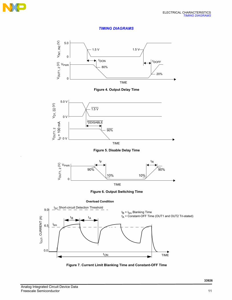
23. Output Delay is the time duration from 1.5 V on the IN1 or IN2 input signal to the 20% or 80% point (dependent on the transition direction) of the OUT1 or OUT2 signal. If the output is transitioning HIGH-to-LOW, the delay is from 1.5 V on the input signal to the 80% point of the output response signal. If the output is transitioning LOW-to-HIGH, the delay is from 1.5 V on the input signal to the 20% point of the output response signal. See Figure 4, page 11.
24. The time during which the internal constant-OFF time PWM current regulation circuit has tri-stated the output bridge. 25. The time during which the current regulation threshold is ignored so that the short-circuit detection threshold comparators may have time
to act.26. Disable Delay Time measurement is defined in Figure 5, page 11.27. Rise Time is from the 10% to the 90% level and Fall Time is from the 90% to the 10% level of the output signal with VPWR = 14 V,
RLOAD = 3.0 ohm. See Figure 6, page 11.
28. Load currents ramping up to the current regulation threshold become limited at the ILIM value (see Figure 7). The short-circuit currents
possess a di/dt that ramps up to the ISCH or ISCL threshold during the ILIM blanking time, registering as a short-circuit event detection and
causing the shutdown circuitry to force the output into an immediate tri-state latch-OFF (see Figure 8). Operation in Current Limit mode may cause junction temperatures to rise. Junction temperatures above ~160C will cause the output current limit threshold to “fold back”, or decrease, until ~175 C is reached, after which the TLIM thermal latch-OFF will occur. Permissible operation within this fold back region
is limited to non-repetitive transient events of duration not to exceed 30 seconds (see Figure 9).29. Parameter is guaranteed by design.
Analog Integrated Circuit Device Data10 Freescale Semiconductor
33926
ELECTRICAL CHARACTERISTICSTIMING DIAGRAMS
TIMING DIAGRAMS
Figure 4. Output Delay Time
Figure 5. Disable Delay Time
.
Figure 6. Output Switching Time
Figure 7. Current Limit Blanking Time and Constant-OFF Time
5.0
VPWR
0
0TIME
1.5 V 1.5 V
20%
80%
tDONV
OU
T1,
2 (
V)
VIN
1, I
N2 (
V)
tDOFF
0 V
5.0 V
0 VVO
UT
1, 2
VD
1, D
2 (V
)
TIME
1.5 V
tDDISABLE
90%
I O =
100
mA
90% 90%
10% 10%
VO
UT
1, 2
(V
)
tF tRVPWR
0
TIME
ISC Short-circuit Detection Threshold
I OU
T, C
UR
RE
NT
(A
) tB
5.0
tA
9.0
0.0
Ilim6.5
tB = Ilim Blanking TimetA = Constant-OFF Time (OUT1 and OUT2 Tri-stated)
Overload Condition
tON TIME
Analog Integrated Circuit Device DataFreescale Semiconductor 11
33926
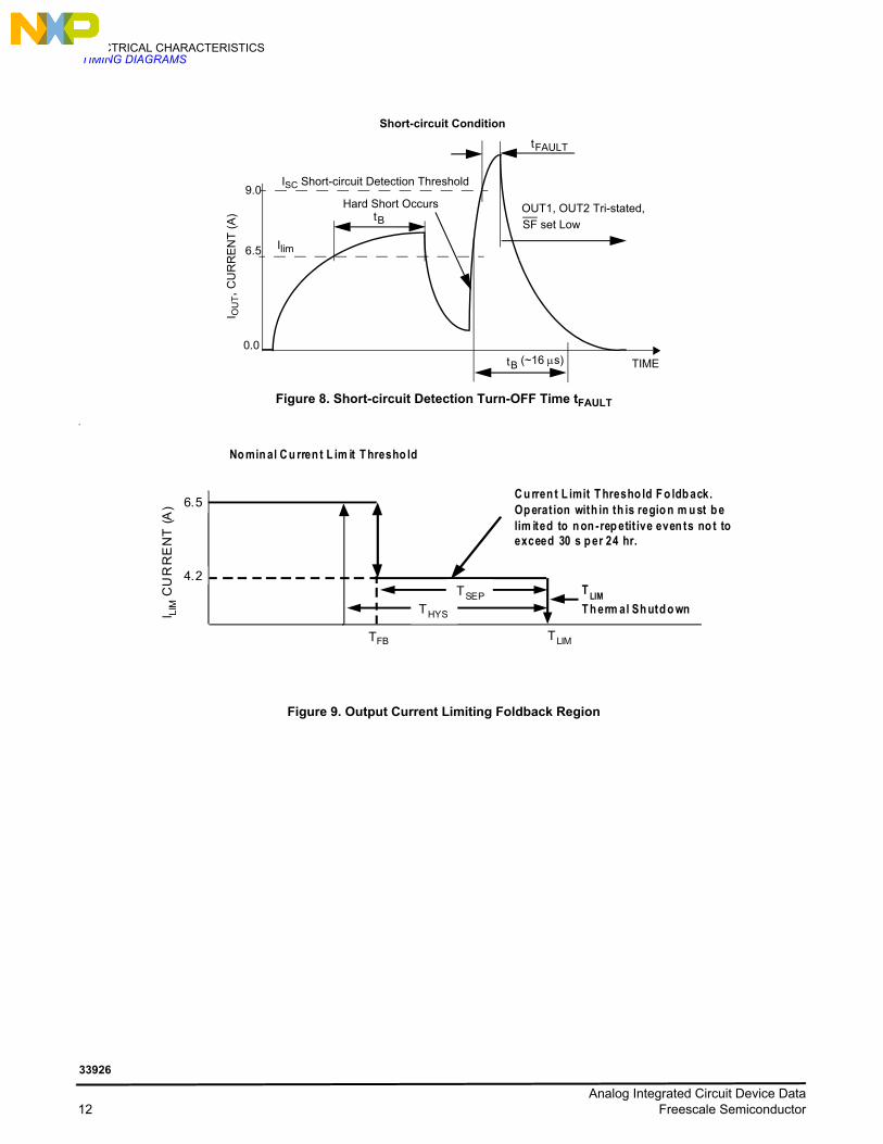
ELECTRICAL CHARACTERISTICSTIMING DIAGRAMS
Figure 8. Short-circuit Detection Turn-OFF Time tFAULT
.
Figure 9. Output Current Limiting Foldback Region
ISC Short-circuit Detection Threshold
I OU
T, C
UR
RE
NT
(A
)
5.0
9.0
0.0
Ilim6.5
Hard Short Occurs
tFAULT
Short-circuit Condition
tB (~16 s)
tB
TIME
SF set Low
OUT1, OUT2 Tri-stated,
TSEP
THYS
TFB TLIM
No min al C u rren t L im it T hresho ld
T LIM
T h erm al Sh utd o wn
Output C urrent Lim iting R egions and Therm al Shutdown
C u rren t L imit T hresho ld F o ldb ack.Op eration with in th is regio n m u st b elim ited to n on -rep etit ive even ts no t toexceed 30 s p er 24 hr.
6.5
4.2
I LIM
CU
RR
EN
T (
A)
Figure 9.
Analog Integrated Circuit Device Data12 Freescale Semiconductor
33926

FUNCTIONAL DESCRIPTIONINTRODUCTION
FUNCTIONAL DESCRIPTION
INTRODUCTION
Numerous protection and operational features (speed, torque, direction, dynamic breaking, PWM control, and closed-loop control) make the 33926 a very attractive, cost-effective solution for controlling a broad range of small DC motors. The 33926 outputs are capable of supporting peak DC load currents of up to 5.0 A from a 28 VPWR source. An internal charge pump and gate drive circuitry are provided that can support external PWM frequencies up to 20 kHz.
The 33926 has an analog feedback (current mirror) output pin (the FB pin) that provides a constant-current source ratioed to the active high-side MOSFETs’ current. This can be used to provide “real time” monitoring of output current to facilitate closed-loop operation for motor speed/torque control, or for the detection of open load conditions.
Two independent inputs, IN1 and IN2, provide control of the two totem-pole half-bridge outputs. An input invert, INV, changes IN1 and IN2 to LOW = true logic. Two different output slew rates are selectable via the SLEW input. Two independent disable inputs, D1 and D2, provide the means to force the H-Bridge outputs to a high-impedance state (all H-Bridge switches OFF). An EN pin controls an enable function that allows the IC to be placed in a power-conserving Sleep mode.
The 33926 has Output Current Limiting (via Constant OFF-Time PWM Current Regulation), Output Short-circuit Detection with Latch-OFF, and Overtemperature Detection with Latch-OFF. Once the device is latched-OFF due to a fault condition, either of the Disable inputs (D1 or D2), VPWR, or EN must be “toggled” to clear the status flag.
Current limiting (Load Current Regulation) is accomplished by a constant-OFF time PWM method using current limit threshold triggering. The current limiting scheme is unique in that it incorporates a junction temperature-dependent current limit threshold. This means that the current limit threshold is “reduced to around 4.2 A” as the junction temperature increases above 160 °C. When the temperature is above 175 °C, overtemperature shutdown (latch-OFF) will occur. This combination of features allows the device to continue operating for short periods of time (< 30 seconds) with unexpected loads, while still retaining adequate protection for both the device and the load.
FUNCTIONAL PIN DESCRIPTION
POWER GROUND AND ANALOG GROUND (PGND AND AGND)The power and analog ground pins should be connected together with a very low-impedance connection.
POSITIVE POWER SUPPLY (VPWR)VPWR pins are the power supply inputs to the device. All VPWR pins must be connected together on the printed circuit board
with as short as possible traces, offering as low-impedance as possible between pins.
Transients on VPWR which go below the undervoltage threshold will result in the protection activating. It is essential to use an input filter capacitor of sufficient size and low ESR to sustain a VPWR greater than VUVLO when the load is switched (See 33926 Typical Application Schematic on page 19).
STATUS FLAG (SF)This pin is the device fault status output. This output is an active LOW open drain structure requiring a pull-up resistor to VDD.
The maximum VDD is < 7.0 V. Refer to Table 6, Truth Table, page 17 for the SF Output status definition.
INPUT INVERT (INV)The Input Invert Control pin sets IN1 and IN2 to LOW = TRUE. This is a Schmitt trigger input with ~ 80 µA sink; the default
condition is non-inverted. If IN1 and IN2 are set so that the current is being commanded to flow through the load attached between OUT1 and OUT2, changing the logic level at INV will have the effect of reversing the direction of current commanded. Thus, the INV input may be used as a “forward/reverse” command input. If both IN1 and IN2 are the same logic level, then changing the logic level at INV will have the effect of changing the bridge’s output from freewheeling high to freewheeling low or vice versa.
SLEW RATE (SLEW)The SLEW pin is the logic input that selects fast or slow slew rate. Schmitt trigger input with ~ 80 µA sink so the default
condition is SLOW. When SLEW is set to SLOW, PWM-ing should be limited to frequencies less than 11 kHz in order to allow the internal high-side driver circuitry time to fully enhance the high-side MOSFETs.
Analog Integrated Circuit Device DataFreescale Semiconductor 13
33926

FUNCTIONAL DESCRIPTIONFUNCTIONAL PIN DESCRIPTION
INPUT 1,2 AND DISABLE INPUT 1,2 (IN1, IN2, AND D1, D2)
These pins are input control pins used to control the outputs. These pins are 3.0 V/ 5.0 V CMOS-compatible inputs with hysteresis. IN1 and IN2 independently control OUT1 and OUT2, respectively. D1 and D2 are complementary inputs used to tri-state disable the H-Bridge outputs.
When either D1 or D2 is SET (D1 = logic HIGH or D2 = logic LOW) in the disable state, outputs OUT1 and OUT2 are both tri-state disabled; however, the rest of the device circuitry is fully operational and the supply IPWR(STANDBY) current is reduced to a few mA. Refer to Table 4, Static Electrical Characteristics, page 8.
H-BRIDGE OUTPUT (OUT1, OUT2)These pins are the outputs of the H-Bridge with integrated freewheeling diodes. The bridge output is controlled using the IN1,
IN2, D1, and D2 inputs. The outputs have PWM current limiting above the ILIM threshold. The outputs also have thermal shutdown (tri-state latch-OFF) with hysteresis as well as short-circuit latch-OFF protection.
A disable timer (time t B) is incorporated to distinguish between load currents that are higher than the ILIM threshold and short-circuit currents. This timer is activated at each output transition.
CHARGE PUMP CAPACITOR (CCP)This pin is the charge pump output pin and connection for the external charge pump reservoir capacitor. The allowable value
is from 30 to 100 nF. This capacitor must be connected from the CCP pin to the VPWR pin. The device cannot operate properly without the external reservoir capacitor.
ENABLE INPUT (EN)The EN pin is used to place the device in a Sleep mode so as to consume very low currents. When the EN pin voltage is a
logic LOW state, the device is in Sleep mode. The device is enabled and fully operational when the EN pin voltage is in logic HIGH. An internal pulldown resistor maintains the device in Sleep mode in the event EN is driven through a high-impedance I/O, or an unpowered microcontroller, or the EN input becomes disconnected.
FEEDBACK (FB)The 33926 has a feedback output (FB) for “real time” monitoring of H-Bridge high-side output currents to facilitate closed-loop
operation for motor speed and torque control.
The FB pin provides current sensing feedback of the H-Bridge high-side drivers. When running in the forward or reverse direction, a ground-referenced 0.24% of load current is output to this pin. Through the use of an external resistor to ground, the proportional feedback current can be converted to a proportional voltage equivalent and the controlling microcontroller can “read” the current proportional voltage with its analog-to-digital converter (ADC). This is intended to provide the user with only first-order motor current feedback for motor torque control. The resistance range for the linear operation of the FB pin is 100 < RFB < 300 .
If PWM-ing is implemented using the disable pin inputs (either D1 or D2), a small filter capacitor (~1.0 µF) may be required in parallel with the RFB resistor to ground for spike suppression.
Analog Integrated Circuit Device Data14 Freescale Semiconductor
33926
FUNCTIONAL INTERNAL BLOCK DESCRIPTIONFUNCTIONAL PIN DESCRIPTION
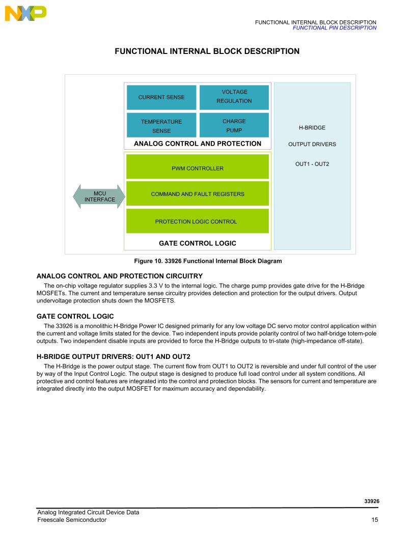
FUNCTIONAL INTERNAL BLOCK DESCRIPTION
Figure 10. 33926 Functional Internal Block Diagram
ANALOG CONTROL AND PROTECTION CIRCUITRYThe on-chip voltage regulator supplies 3.3 V to the internal logic. The charge pump provides gate drive for the H-Bridge
MOSFETs. The current and temperature sense circuitry provides detection and protection for the output drivers. Output undervoltage protection shuts down the MOSFETS.
GATE CONTROL LOGICThe 33926 is a monolithic H-Bridge Power IC designed primarily for any low voltage DC servo motor control application within
the current and voltage limits stated for the device. Two independent inputs provide polarity control of two half-bridge totem-pole outputs. Two independent disable inputs are provided to force the H-Bridge outputs to tri-state (high-impedance off-state).
H-BRIDGE OUTPUT DRIVERS: OUT1 AND OUT2The H-Bridge is the power output stage. The current flow from OUT1 to OUT2 is reversible and under full control of the user
by way of the Input Control Logic. The output stage is designed to produce full load control under all system conditions. All protective and control features are integrated into the control and protection blocks. The sensors for current and temperature are integrated directly into the output MOSFET for maximum accuracy and dependability.
MCUINTERFACE
PROTECTION LOGIC CONTROL
COMMAND AND FAULT REGISTERS
GATE CONTROL LOGIC
CURRENT SENSEVOLTAGE
REGULATION
TEMPERATURE
SENSE
CHARGE
PUMP H-BRIDGE
OUTPUT DRIVERS
OUT1 - OUT2
ANALOG CONTROL AND PROTECTION
PWM CONTROLLER
Analog Integrated Circuit Device DataFreescale Semiconductor 15
33926

FUNCTIONAL DEVICE OPERATIONOPERATIONAL MODES
FUNCTIONAL DEVICE OPERATION
OPERATIONAL MODES
Figure 11. Operating States
PWMCurrentLimiting
9.0
6.5
Typical Short-circuit Detection Threshold
Typical Current Limit Threshold
Hard Short Detection and Latch-OFF
0
IN1 or IN2
IN2 or IN1
IN1 or IN2
IN2 or IN1IN1 IN2
[1]
[0]
[1]
[0]
[1]
[0]
[1]
[0]
OutputsTri-stated
OutputsTri-stated
Outputs Operation(per Input Control Condition)
Time
SF
, LO
GIC
OU
TD
2, L
OG
IC I
ND
1, L
OG
IC IN
INn,
LO
GIC
INI L
OA
D, O
UT
PU
T C
UR
RE
NT
(A
)
High Current Load Being Regulated via Constant-OFF-Time PWM
Moderate Current Load
Analog Integrated Circuit Device Data16 Freescale Semiconductor
33926

FUNCTIONAL DEVICE OPERATIONLOGIC COMMANDS AND REGISTERS
LOGIC COMMANDS AND REGISTERS
Figure 12. 33926 Power Stage Operation
Table 6. Truth Table
The tri-state conditions and the status flag are reset using D1 or D2. The truth table uses the following notations: L = LOW, H = HIGH, X = HIGH or LOW, and Z = High-impedance. All output power transistors are switched off.
Device StateInput Conditions Status Outputs
EN D1 D2 IN1 IN2 SF OUT1 OUT2
Forward H L H H L H H L
Reverse H L H L H H L H
Free Wheeling Low H L H L L H L L
Free Wheeling High H L H H H H H H
Disable 1 (D1) H H X X X L Z Z
Disable 2 (D2) H X L X X L Z Z
IN1 Disconnected H L H Z X H H X
IN2 Disconnected H L H X Z H X H
D1 Disconnected H Z X X X L Z Z
D2 Disconnected H X Z X X L Z Z
Undervoltage Lockout (30) H X X X X L Z Z
Overtemperature (31) H X X X X L Z Z
Short-circuit (31) H X X X X L Z Z
Sleep Mode EN L X X X X H Z Z
EN Disconnected Z X X X X H Z Z
Notes30. In the event of an undervoltage condition, the outputs tri-state and status flag is SET logic LOW. Upon undervoltage recovery, status
flag is reset automatically or automatically cleared and the outputs are restored to their original operating condition.31. When a short-circuit or overtemperature condition is detected, the power outputs are tri-state latched-OFF, independent of the input
signals, and the status flag is latched to logic LOW. To reset from this condition requires the toggling of either D1, D2, EN, or VPWR.
OUT1 OUT2
PGND
VPWRVPW R
PGND
LOAD
LoadCurrent
Forward
OFF
ON
ON
OFF
OUT1 OUT2
PGND
OFF
ON
ON
OFF
VPWR VPW R
PGND
LOAD
LoadCurrent
Reverse
OUT1 OUT2
PGND
VPWRVPWR
PGND
LOAD
LoadCurrent
High-Side Recirculation(Forward)
ON
OFF
ON
OFF
OUT1 OUT2
PGND
VPWRVPWR
PGND
LOAD
LoadCurrent
Low-Side Recirculation(Forward)
ON ON
OFF OFF
Analog Integrated Circuit Device DataFreescale Semiconductor 17
33926
FUNCTIONAL DEVICE OPERATIONPROTECTION AND DIAGNOSTIC FEATURES
PROTECTION AND DIAGNOSTIC FEATURES
SHORT-CIRCUIT PROTECTIONIf an output short-circuit condition is detected, the power outputs tri-state (latch-OFF) independent of the input (IN1 and IN2)
states, and the fault status output flag (SF) is SET to a logic LOW. If the D1 input changes from a logic HIGH to logic LOW, or if the D2 input changes from a logic LOW to logic HIGH, the output bridge will become operational again, and the fault status flag will be reset (cleared) to a logic HIGH state.
The output stage will always switch into the mode defined by the input pins (IN1, IN2, D1, and D2), provided the device junction temperature is within the specified operating temperature range.
INTERNAL PWM CURRENT LIMITINGThe maximum current flow under normal operating conditions should be less than 5.0 A. The instantaneous load currents will
be limited to ILIM via the internal PWM current limiting circuitry. When the ILIM threshold current value is reached, the output stages are tri-stated for a fixed time (T A) of 20 µs typical. Depending on the time constant associated with the load characteristics, the output current decreases during the tri-state duration until the next output ON cycle occurs.
The PWM current limit threshold value is dependent on the device junction temperature. When - 40 °C < TJ < 160 °C, ILIM is between the specified minimum/maximum values. When TJ exceeds 160 °C, the ILIM threshold decreases to 4.2 A. Shortly above 175 °C the device overtemperature circuit will detect TLIM and an overtemperature shutdown will occur. This feature implements a graceful degradation of operation before thermal shutdown occurs, thus allowing for intermittent unexpected mechanical loads on the motor’s gear-reduction train to be handled.
Important Die temperature excursions above 150 C are permitted only for non-repetitive durations < 30 seconds. Provision must be made at the system level to prevent prolonged operation in the current-foldback region.
OVERTEMPERATURE SHUTDOWN AND HYSTERESISIf an overtemperature condition occurs, the power outputs are tri-stated (latched-OFF), and the fault status flag (SF) is SET to
a logic LOW.
To reset from this condition, D1 must change from a logic HIGH to logic LOW, or D2 must change from a logic LOW to logic HIGH. When reset, the output stage switches ON again, provided that the junction temperature is now below the overtemperature threshold limit minus the hysteresis.
Important Resetting from the fault condition will clear the fault status flag. Powering down and powering up the device will also reset the 33926 from the fault condition.
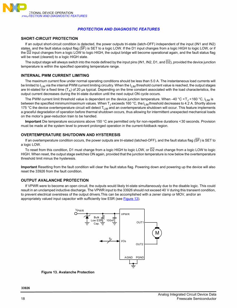
OUTPUT AVALANCHE PROTECTIONIf VPWR were to become an open circuit, the outputs would likely tri-state simultaneously due to the disable logic. This could
result in an unclamped inductive discharge. The VPWR input to the 33926 should not exceed 40 V during this transient condition, to prevent electrical overstress of the output drivers.This can be accomplished with a zener clamp or MOV, and/or an appropriately valued input capacitor with sufficiently low ESR (see Figure 13).
Figure 13. Avalanche Protection
OUT1
OUT2I/Os
AGND PGND
BulkLow ESR
Cap.
VPWR
100nF
M
VPWR
9
Analog Integrated Circuit Device Data18 Freescale Semiconductor
33926

TYPICAL APPLICATIONSINTRODUCTION
TYPICAL APPLICATIONS
INTRODUCTION
A typical application schematic is shown in Figure 14. For precision high current applications in harsh, noisy environments, the VPWR by-pass capacitor may need to be substantially larger.
Figure 14. 33926 Typical Application Schematic
VDDLOGIC SUPPLY
CHARGEPUMP
GATE DRIVEAND
PROTECTIONLOGIC
CURRENT MIRRORSAND
CONSTANT OFF-TIMEPWM CURRENT REGULATOR
VCP
CCP OUT1
OUT2
AGND
TO GATES
HS1
LS1
HS2
LS2
VPWR
VSENSE
ILIM PWM
HS1 HS2
LS1 LS2LS2EN
IN1
IN2
D2
D1
INV
SLEW
SF
FB
PGND
+5.0 V
RFB270
STATUSFLAG
TOADC
1.0 F
33 nF
VPWR
100 nF 100 F
M
PGND
LOW ESR
Analog Integrated Circuit Device DataFreescale Semiconductor 19
33926
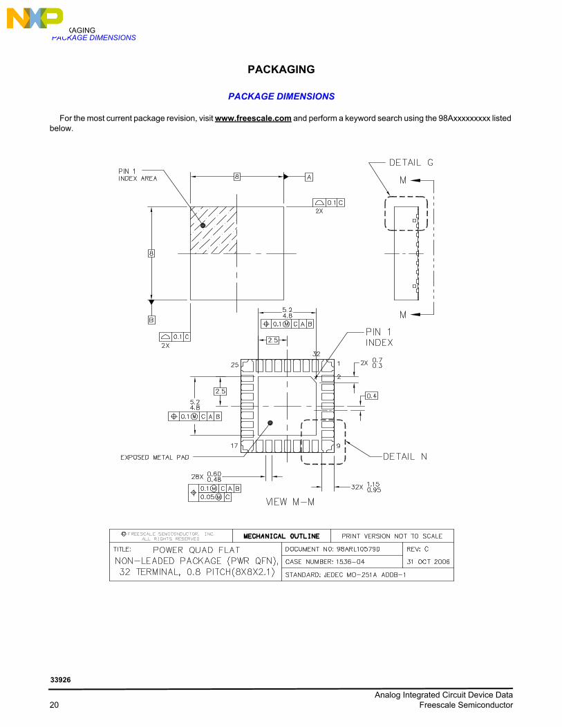
PACKAGINGPACKAGE DIMENSIONS
PACKAGING
PACKAGE DIMENSIONS
For the most current package revision, visit www.freescale.com and perform a keyword search using the 98Axxxxxxxxx listed below.
Analog Integrated Circuit Device Data20 Freescale Semiconductor
33926
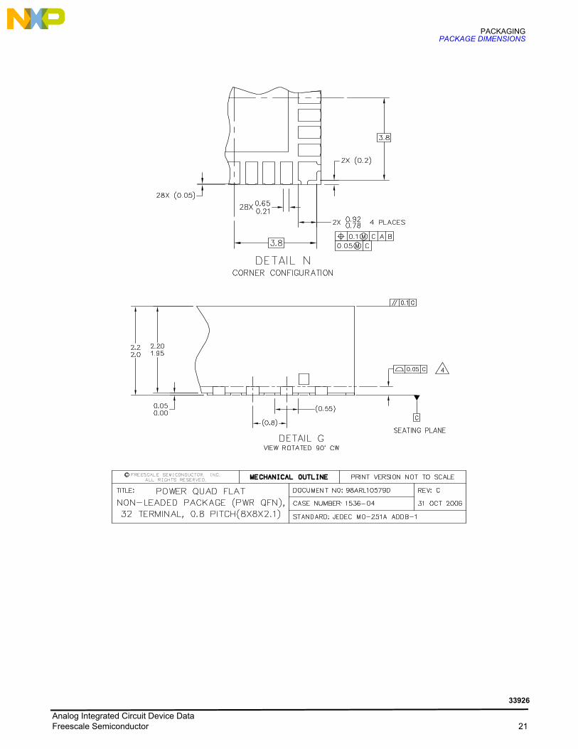
PACKAGINGPACKAGE DIMENSIONS
Analog Integrated Circuit Device DataFreescale Semiconductor 21
33926
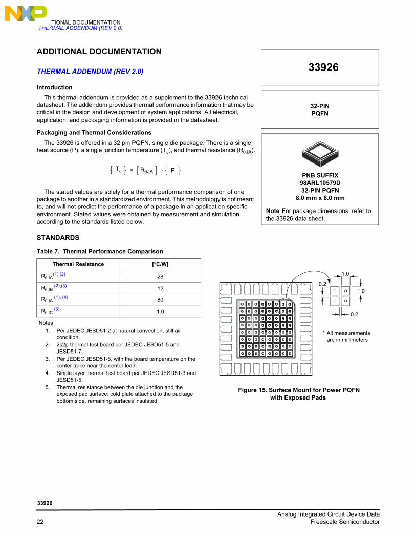
ADDITIONAL DOCUMENTATIONTHERMAL ADDENDUM (REV 2.0)
ADDITIONAL DOCUMENTATION
THERMAL ADDENDUM (REV 2.0)
Introduction
This thermal addendum is provided as a supplement to the 33926 technical datasheet. The addendum provides thermal performance information that may be critical in the design and development of system applications. All electrical, application, and packaging information is provided in the datasheet.
Packaging and Thermal Considerations
The 33926 is offered in a 32 pin PQFN, single die package. There is a single heat source (P), a single junction temperature (TJ), and thermal resistance (RJA).
The stated values are solely for a thermal performance comparison of one package to another in a standardized environment. This methodology is not meant to, and will not predict the performance of a package in an application-specific environment. Stated values were obtained by measurement and simulation according to the standards listed below.
STANDARDS
Figure 15. Surface Mount for Power PQFNwith Exposed Pads
32-PINPQFN
33926
PNB SUFFIX98ARL10579D32-PIN PQFN
8.0 mm x 8.0 mm
Note For package dimensions, refer to the 33926 data sheet.
TJ = RJA . P
Table 7. Thermal Performance Comparison
Thermal Resistance [C/W]
RJA(1),(2) 28
RJB (2),(3) 12
RJA (1), (4) 80
RJC(5) 1.0
Notes1. Per JEDEC JESD51-2 at natural convection, still air
condition.2. 2s2p thermal test board per JEDEC JESD51-5 and
JESD51-7.3. Per JEDEC JESD51-8, with the board temperature on the
center trace near the center lead.4. Single layer thermal test board per JEDEC JESD51-3 and
JESD51-5.5. Thermal resistance between the die junction and the
exposed pad surface; cold plate attached to the package bottom side, remaining surfaces insulated.
1.0
1.00.2
0.2
* All measurementsare in millimeters
Analog Integrated Circuit Device Data22 Freescale Semiconductor
33926

ADDITIONAL DOCUMENTATIONTHERMAL ADDENDUM (REV 2.0)
Figure 16. Thermal Test Board
Device on Thermal Test Board Table 8. Thermal Resistance Performance
RJA is the thermal resistance between die junction and ambient air.
33926PNB Pin Connections
32-Pin PQFN0.80 mm Pitch
8.0 mm x 8.0 mm Body
A
25
17
18
19
20
21
22
23
24
9 10 11 12 13 14 15 16
1
2
3
4
5
6
7
8
26272829303132 NC
NC
VP
WR
NC
IN2
IN1
SLEW
OU
T1
AGND
INV
FB
EN
OU
T1
VPWR
VPWR
OU
T2
OU
T2
AGND
OU
T1
D2
PGND
SF
D1
OU
T2
OU
T2
CC
P
VP
WR
PGND
PGND
PGND
PGND
PGND
OU
T1
Material: Single layer printed circuit board
FR4, 1.6 mm thickness
Cu traces, 0.07 mm thickness
Outline: 80 mm x 100 mm board area, including edge connector for thermal testing
Area A: Cu heat-spreading areas on board surface
Ambient Conditions: Natural convection, still air
A [mm2] RJA [C/W]
0 81
300 49
600 40
Analog Integrated Circuit Device DataFreescale Semiconductor 23
33926
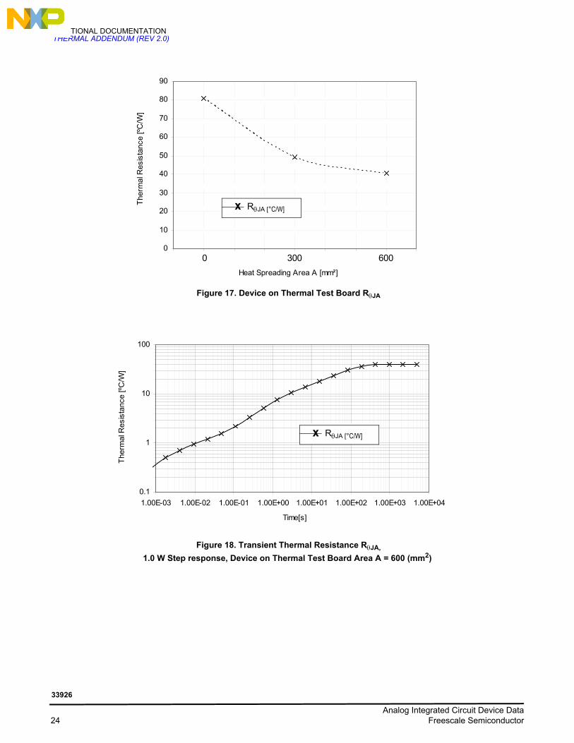
ADDITIONAL DOCUMENTATIONTHERMAL ADDENDUM (REV 2.0)
Figure 17. Device on Thermal Test Board RJA
Figure 18. Transient Thermal Resistance RJA,
1.0 W Step response, Device on Thermal Test Board Area A = 600 (mm2)
0
10
20
30
40
50
60
70
80
90
Heat Spreading Area A [mm²]
The
rmal
Res
ista
nce
[ºC
/W]
0 300 600
RJA [°C/W]x
0.1
1
10
100
1.00E-03 1.00E-02 1.00E-01 1.00E+00 1.00E+01 1.00E+02 1.00E+03 1.00E+04
Time[s]
The
rmal
Res
ista
nce
[ºC
/W]
RJA [°C/W]x
Analog Integrated Circuit Device Data24 Freescale Semiconductor
33926
REVISION HISTORYTHERMAL ADDENDUM (REV 2.0)
REVISION HISTORY
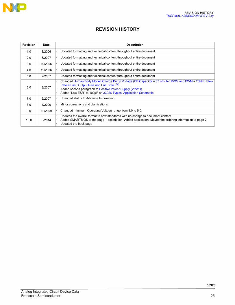
Revision Date Description
1.0 3/2006 • Updated formatting and technical content throughout entire document.
2.0 6/2007 • Updated formatting and technical content throughout entire document
3.0 10/2006 • Updated formatting and technical content throughout entire document
4.0 12/2006 • Updated formatting and technical content throughout entire document
5.0 2/2007 • Updated formatting and technical content throughout entire document
6.0 3/2007
• Changed Human Body Model, Charge Pump Voltage (CP Capacitor = 33 nF), No PWM and PWM = 20kHz, Slew Rate = Fast, Output Rise and Fall Time (27)
• Added second paragraph to Positive Power Supply (VPWR)• Added “Low ESR” to 100F on 33926 Typical Application Schematic
7.0 6/2007 • Changed status to Advance Information
8.0 4/2009 • Minor corrections and clarifications.
9.0 12/2009 • Changed minimum Operating Voltage range from 8.0 to 5.0.
10.0 8/2014• Updated the overall format to new standards with no change to document content• Added SMARTMOS to the page 1 description. Added application. Moved the ordering information to page 2• Updated the back page
Analog Integrated Circuit Device DataFreescale Semiconductor 25
33926

Document Number: MC33926Rev. 10.0
8/2014
Information in this document is provided solely to enable system and software implementers to use Freescale products.
There are no express or implied copyright licenses granted hereunder to design or fabricate any integrated circuits based
on the information in this document.
Freescale reserves the right to make changes without further notice to any products herein. Freescale makes no
warranty, representation, or guarantee regarding the suitability of its products for any particular purpose, nor does
Freescale assume any liability arising out of the application or use of any product or circuit, and specifically disclaims any
and all liability, including without limitation consequential or incidental damages. “Typical” parameters that may be
provided in Freescale data sheets and/or specifications can and do vary in different applications, and actual performance
may vary over time. All operating parameters, including “typicals,” must be validated for each customer application by
customer’s technical experts. Freescale does not convey any license under its patent rights nor the rights of others.
Freescale sells products pursuant to standard terms and conditions of sale, which can be found at the following address:
freescale.com/SalesTermsandConditions.
Freescale and the Freescale logo are trademarks of Freescale Semiconductor, Inc., Reg. U.S. Pat. & Tm. Off.
SMARTMOS is a trademark of Freescale Semiconductor, Inc. All other product or service names are the property of their
respective owners.
© 2014 Freescale Semiconductor, Inc.
How to Reach Us:
Home Page: freescale.com
Web Support: freescale.com/support