MC33078 DUAL HIGH-SPEEDLOW-NOISEOPERATIONAL AMPLIFIER - TI.com · Electrical Characteristics...
24
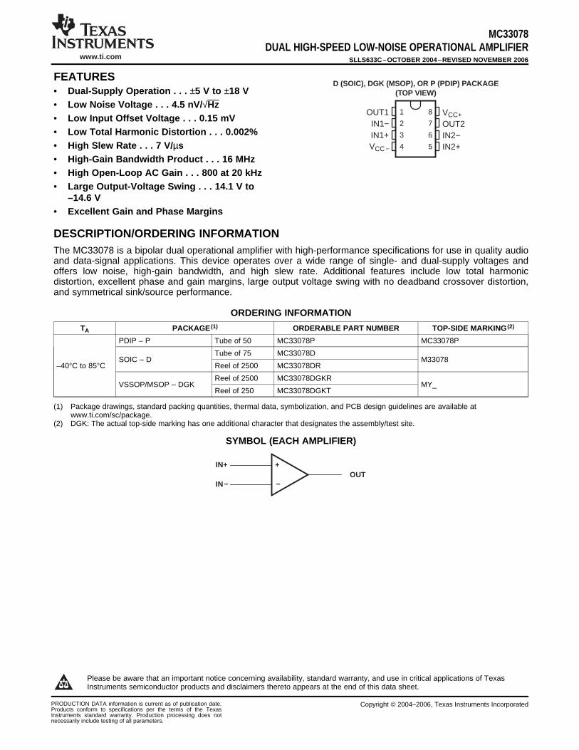
www.ti.com FEATURES 1 2 3 4 8 7 6 5 OUT1 IN1- IN1+ V CC - V CC+ OUT2 IN2- IN2+ D (SOIC), DGK (MSOP), OR P (PDIP) PACKAGE (TOP VIEW) DESCRIPTION/ORDERING INFORMATION IN+ IN- OUT + - MC33078 DUAL HIGH-SPEED LOW-NOISE OPERATIONAL AMPLIFIER SLLS633C – OCTOBER 2004 – REVISED NOVEMBER 2006 • Dual-Supply Operation . . . ±5 V to ±18 V • Low Noise Voltage . . . 4.5 nV/√Hz • Low Input Offset Voltage . . . 0.15 mV • Low Total Harmonic Distortion . . . 0.002% • High Slew Rate . . . 7 V/μs • High-Gain Bandwidth Product . . . 16 MHz • High Open-Loop AC Gain . . . 800 at 20 kHz • Large Output-Voltage Swing . . . 14.1 V to –14.6 V • Excellent Gain and Phase Margins The MC33078 is a bipolar dual operational amplifier with high-performance specifications for use in quality audio and data-signal applications. This device operates over a wide range of single- and dual-supply voltages and offers low noise, high-gain bandwidth, and high slew rate. Additional features include low total harmonic distortion, excellent phase and gain margins, large output voltage swing with no deadband crossover distortion, and symmetrical sink/source performance. ORDERING INFORMATION T A PACKAGE (1) ORDERABLE PART NUMBER TOP-SIDE MARKING (2) PDIP – P Tube of 50 MC33078P MC33078P Tube of 75 MC33078D SOIC – D M33078 –40°C to 85°C Reel of 2500 MC33078DR Reel of 2500 MC33078DGKR VSSOP/MSOP – DGK MY_ Reel of 250 MC33078DGKT (1) Package drawings, standard packing quantities, thermal data, symbolization, and PCB design guidelines are available at www.ti.com/sc/package. (2) DGK: The actual top-side marking has one additional character that designates the assembly/test site. SYMBOL (EACH AMPLIFIER) Please be aware that an important notice concerning availability, standard warranty, and use in critical applications of Texas Instruments semiconductor products and disclaimers thereto appears at the end of this data sheet. PRODUCTION DATA information is current as of publication date. Copyright © 2004–2006, Texas Instruments Incorporated Products conform to specifications per the terms of the Texas Instruments standard warranty. Production processing does not necessarily include testing of all parameters.
Transcript of MC33078 DUAL HIGH-SPEEDLOW-NOISEOPERATIONAL AMPLIFIER - TI.com · Electrical Characteristics...
www.ti.com
FEATURES
1
2
3
4
8
7
6
5
OUT1IN1−IN1+VCC −
VCC+OUT2IN2−IN2+
D (SOIC), DGK (MSOP), OR P (PDIP) PACKAGE(TOP VIEW)
DESCRIPTION/ORDERING INFORMATION
IN+
IN−OUT
+
−
MC33078DUAL HIGH-SPEED LOW-NOISE OPERATIONAL AMPLIFIER
SLLS633C–OCTOBER 2004–REVISED NOVEMBER 2006
• Dual-Supply Operation . . . ±5 V to ±18 V• Low Noise Voltage . . . 4.5 nV/√Hz• Low Input Offset Voltage . . . 0.15 mV• Low Total Harmonic Distortion . . . 0.002%• High Slew Rate . . . 7 V/µs• High-Gain Bandwidth Product . . . 16 MHz• High Open-Loop AC Gain . . . 800 at 20 kHz• Large Output-Voltage Swing . . . 14.1 V to
–14.6 V• Excellent Gain and Phase Margins
The MC33078 is a bipolar dual operational amplifier with high-performance specifications for use in quality audioand data-signal applications. This device operates over a wide range of single- and dual-supply voltages andoffers low noise, high-gain bandwidth, and high slew rate. Additional features include low total harmonicdistortion, excellent phase and gain margins, large output voltage swing with no deadband crossover distortion,and symmetrical sink/source performance.
ORDERING INFORMATION
TA PACKAGE (1) ORDERABLE PART NUMBER TOP-SIDE MARKING (2)
PDIP – P Tube of 50 MC33078P MC33078P
Tube of 75 MC33078DSOIC – D M33078
–40°C to 85°C Reel of 2500 MC33078DR
Reel of 2500 MC33078DGKRVSSOP/MSOP – DGK MY_
Reel of 250 MC33078DGKT
(1) Package drawings, standard packing quantities, thermal data, symbolization, and PCB design guidelines are available atwww.ti.com/sc/package.
(2) DGK: The actual top-side marking has one additional character that designates the assembly/test site.
SYMBOL (EACH AMPLIFIER)
Please be aware that an important notice concerning availability, standard warranty, and use in critical applications of TexasInstruments semiconductor products and disclaimers thereto appears at the end of this data sheet.
PRODUCTION DATA information is current as of publication date. Copyright © 2004–2006, Texas Instruments IncorporatedProducts conform to specifications per the terms of the TexasInstruments standard warranty. Production processing does notnecessarily include testing of all parameters.
www.ti.com
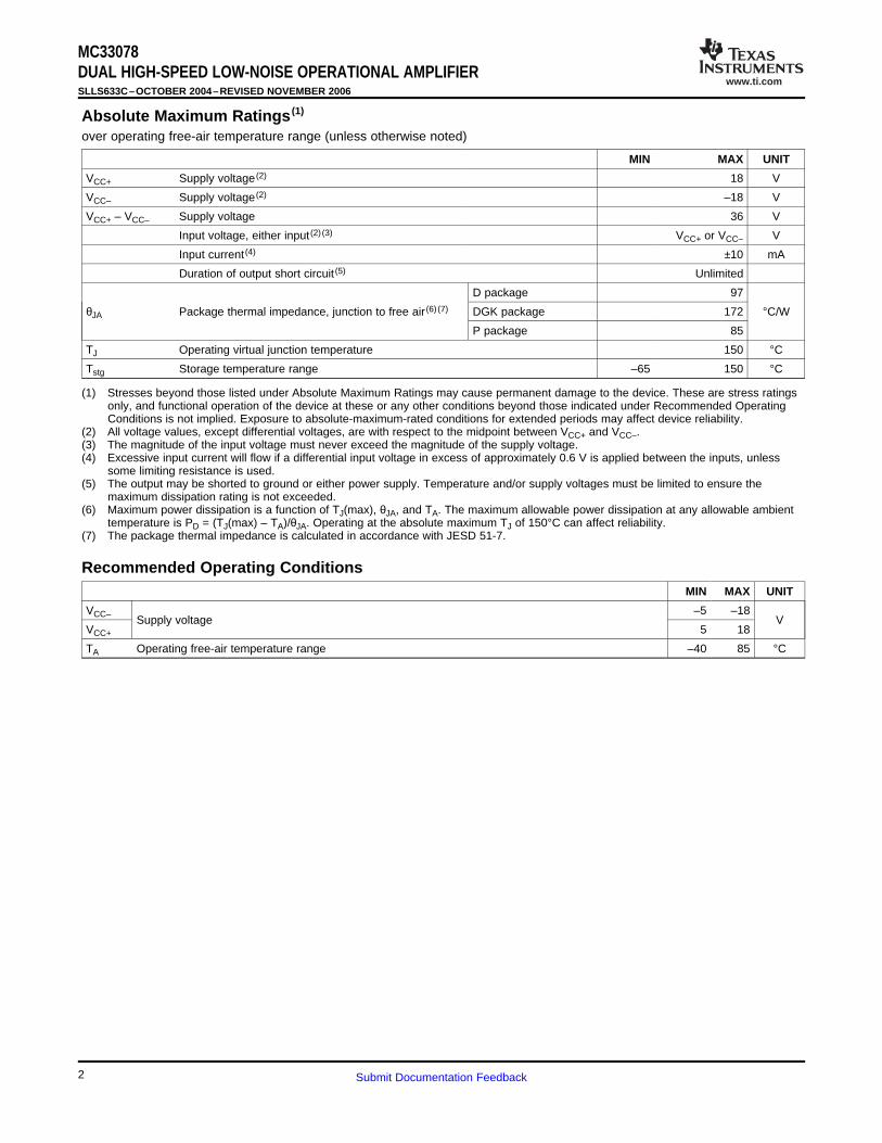
Absolute Maximum Ratings (1)
Recommended Operating Conditions
MC33078DUAL HIGH-SPEED LOW-NOISE OPERATIONAL AMPLIFIERSLLS633C–OCTOBER 2004–REVISED NOVEMBER 2006
over operating free-air temperature range (unless otherwise noted)
MIN MAX UNIT
VCC+ Supply voltage (2) 18 V
VCC– Supply voltage (2) –18 V
VCC+ – VCC– Supply voltage 36 V
Input voltage, either input (2) (3) VCC+ or VCC– V
Input current (4) ±10 mA
Duration of output short circuit (5) Unlimited
D package 97
θJA Package thermal impedance, junction to free air (6) (7) DGK package 172 °C/W
P package 85
TJ Operating virtual junction temperature 150 °C
Tstg Storage temperature range –65 150 °C
(1) Stresses beyond those listed under Absolute Maximum Ratings may cause permanent damage to the device. These are stress ratingsonly, and functional operation of the device at these or any other conditions beyond those indicated under Recommended OperatingConditions is not implied. Exposure to absolute-maximum-rated conditions for extended periods may affect device reliability.
(2) All voltage values, except differential voltages, are with respect to the midpoint between VCC+ and VCC–.(3) The magnitude of the input voltage must never exceed the magnitude of the supply voltage.(4) Excessive input current will flow if a differential input voltage in excess of approximately 0.6 V is applied between the inputs, unless
some limiting resistance is used.(5) The output may be shorted to ground or either power supply. Temperature and/or supply voltages must be limited to ensure the
maximum dissipation rating is not exceeded.(6) Maximum power dissipation is a function of TJ(max), θJA, and TA. The maximum allowable power dissipation at any allowable ambient
temperature is PD = (TJ(max) – TA)/θJA. Operating at the absolute maximum TJ of 150°C can affect reliability.(7) The package thermal impedance is calculated in accordance with JESD 51-7.
MIN MAX UNIT
VCC– –5 –18Supply voltage V
VCC+ 5 18
TA Operating free-air temperature range –40 85 °C
2 Submit Documentation Feedback
www.ti.com
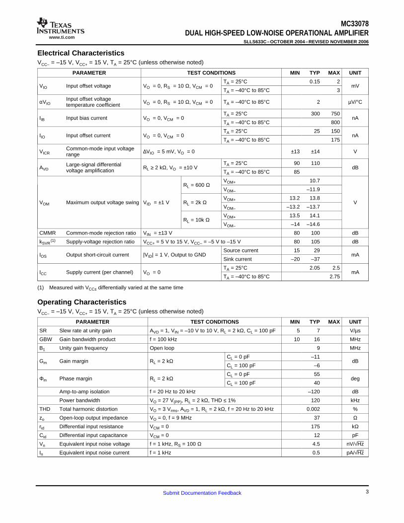
Electrical Characteristics
Operating Characteristics
MC33078DUAL HIGH-SPEED LOW-NOISE OPERATIONAL AMPLIFIER
SLLS633C–OCTOBER 2004–REVISED NOVEMBER 2006
VCC– = –15 V, VCC+ = 15 V, TA = 25°C (unless otherwise noted)
PARAMETER TEST CONDITIONS MIN TYP MAX UNIT
TA = 25°C 0.15 2VIO Input offset voltage VO = 0, RS = 10 Ω, VCM = 0 mV
TA = –40°C to 85°C 3
Input offset voltageαVIO VO = 0, RS = 10 Ω, VCM = 0 TA = –40°C to 85°C 2 µV/°Ctemperature coefficient
TA = 25°C 300 750IIB Input bias current VO = 0, VCM = 0 nA
TA = –40°C to 85°C 800
TA = 25°C 25 150IIO Input offset current VO = 0, VCM = 0 nA
TA = –40°C to 85°C 175
Common-mode input voltageVICR ∆VIO = 5 mV, VO = 0 ±13 ±14 Vrange
TA = 25°C 90 110Large-signal differentialAVD RL ≥ 2 kΩ, VO = ±10 V dBvoltage amplification TA = –40°C to 85°C 85
VOM+ 10.7RL = 600 Ω
VOM– –11.9
VOM+ 13.2 13.8VOM Maximum output voltage swing VID = ±1 V RL = 2k Ω V
VOM– –13.2 –13.7
VOM+ 13.5 14.1RL = 10k Ω
VOM– –14 –14.6
CMMR Common-mode rejection ratio VIN = ±13 V 80 100 dB
kSVR(1) Supply-voltage rejection ratio VCC+ = 5 V to 15 V, VCC– = –5 V to –15 V 80 105 dB
Source current 15 29IOS Output short-circuit current |VID| = 1 V, Output to GND mA
Sink current –20 –37
TA = 25°C 2.05 2.5ICC Supply current (per channel) VO = 0 mA
TA = –40°C to 85°C 2.75
(1) Measured with VCC± differentially varied at the same time
VCC– = –15 V, VCC+ = 15 V, TA = 25°C (unless otherwise noted)
PARAMETER TEST CONDITIONS MIN TYP MAX UNIT
SR Slew rate at unity gain AVD = 1, VIN = –10 V to 10 V, RL = 2 kΩ, CL = 100 pF 5 7 V/µs
GBW Gain bandwidth product f = 100 kHz 10 16 MHz
B1 Unity gain frequency Open loop 9 MHz
CL = 0 pF –11Gm Gain margin RL = 2 kΩ dB
CL = 100 pF –6
CL = 0 pF 55Φm Phase margin RL = 2 kΩ deg
CL = 100 pF 40
Amp-to-amp isolation f = 20 Hz to 20 kHz –120 dB
Power bandwidth VO = 27 V(PP), RL = 2 kΩ, THD ≤ 1% 120 kHz
THD Total harmonic distortion VO = 3 Vrms, AVD = 1, RL = 2 kΩ, f = 20 Hz to 20 kHz 0.002 %
zo Open-loop output impedance VO = 0, f = 9 MHz 37 Ω
rid Differential input resistance VCM = 0 175 kΩ
Cid Differential input capacitance VCM = 0 12 pF
Vn Equivalent input noise voltage f = 1 kHz, RS = 100 Ω 4.5 nV/√Hz
In Equivalent input noise current f = 1 kHz 0.5 pA/√Hz
3Submit Documentation Feedback
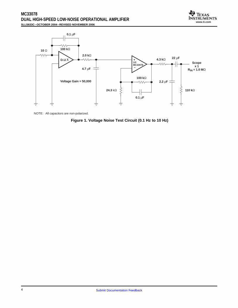
www.ti.com
D.U.T.
Voltage Gain = 50,000
Scopex 1
RIN = 1.0 MΩ
+
−
100 kΩ10 Ω
0.1 µF
100 kΩ
0.1 µF
24.3 kΩ
4.7 µF
2.0 kΩ
2.2 µF
22 µF
110 kΩ
4.3 kΩ1/2MC33078
NOTE: All capacitors are non-polarized.
MC33078DUAL HIGH-SPEED LOW-NOISE OPERATIONAL AMPLIFIERSLLS633C–OCTOBER 2004–REVISED NOVEMBER 2006
Figure 1. Voltage Noise Test Circuit (0.1 Hz to 10 Hz)
4 Submit Documentation Feedback
www.ti.com
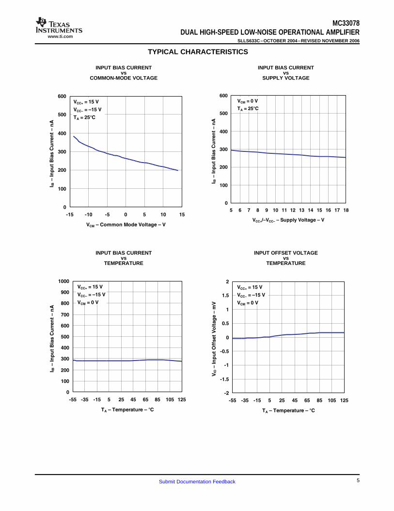
TYPICAL CHARACTERISTICS
0
100
200
300
400
500
600
5 6 7 8 9 10 11 12 13 14 15 16 17 18
VCC+/–VCC– – Supply Voltage – V
I IB–
Inp
ut
Bia
sC
urr
en
t–
nA
VCM = 0 V
TA = 25°C
0
100
200
300
400
500
600
-15 -10 -5 0 5 10 15
VCM – Common Mode Voltage – V
I IB–
Inp
ut
Bia
sC
urr
en
t–
nA
VCC+ = 15 V
VCC– = –15 V
TA = 25°C
0
100
200
300
400
500
600
700
800
900
1000
-55 -35 -15 5 25 45 65 85 105 125
TA – Temperature – °C
I IB–
Inp
ut
Bia
sC
urr
en
t–
nA
VCC+ = 15 V
VCC– = –15 V
VCM = 0 V
-2
-1.5
-1
-0.5
0
0.5
1
1.5
2
-55 -35 -15 5 25 45 65 85 105 125
TA – Temperature – °C
VIO
–In
pu
tO
ffset
Vo
ltag
e–
mV
VCC+ = 15 V
VCC– = –15 V
VCM = 0 V
MC33078DUAL HIGH-SPEED LOW-NOISE OPERATIONAL AMPLIFIER
SLLS633C–OCTOBER 2004–REVISED NOVEMBER 2006
INPUT BIAS CURRENT INPUT BIAS CURRENTvs vs
COMMON-MODE VOLTAGE SUPPLY VOLTAGE
INPUT BIAS CURRENT INPUT OFFSET VOLTAGEvs vs
TEMPERATURE TEMPERATURE
5Submit Documentation Feedback
www.ti.com
0
0.2
0.4
0.6
0.8
1
1.2
1.4
-55 -25 5 35 65 95 125
TA – Temperature – °C
Inp
ut
Co
mm
on
-Mo
de
Vo
ltag
eL
ow
Pro
xim
ity
toV
CC
––
V
VCC+ = 3 V to 15 V
VCC– = -3 V to -15 V
è VIO = 5 mV
VO = 0 V
D
-1.4
-1.2
-1
-0.8
-0.6
-0.4
-0.2
0
-55 -25 5 35 65 95 125
TA – Temperature – °C
Inp
ut
Co
mm
on
-Mo
de
Vo
ltag
eH
igh
Pro
xim
ity
toV
CC
+–
V
VCC+ = 3 V to 15 V
VCC– = -3 V to -15 V
VIO = 5 mV
VO = 0 V
D
0
1
2
3
4
5
6
7
8
9
10
0 0.5 1 1.5 2 2.5 3 3.5 4 4.5
RL – Load Resistance – k@
Ou
tpu
tS
atu
rati
on
Vo
ltag
e
Pro
xim
ity
toV
CC
––
V
T = –55°CA
T = 25°CA
T = 125°CA
kW
-10
-9
-8
-7
-6
-5
-4
-3
-2
-1
0
0 0.5 1 1.5 2 2.5 3 3.5 4 4.5
RL – Load Resistance – kh
Ou
tpu
tS
atu
rati
on
Vo
ltag
e
Pro
xim
ity
toV
CC
+–
V
T = –55°CA
T = 25°CA
T = 125°CA
kW
MC33078DUAL HIGH-SPEED LOW-NOISE OPERATIONAL AMPLIFIERSLLS633C–OCTOBER 2004–REVISED NOVEMBER 2006
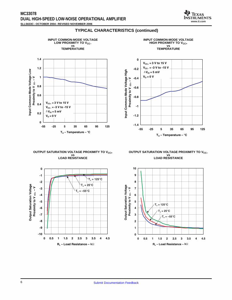
TYPICAL CHARACTERISTICS (continued)
INPUT COMMON-MODE VOLTAGE INPUT COMMON-MODE VOLTAGELOW PROXIMITY TO VCC– HIGH PROXIMITY TO VCC+
vs vsTEMPERATURE TEMPERATURE
OUTPUT SATURATION VOLTAGE PROXIMITY TO VCC+ OUTPUT SATURATION VOLTAGE PROXIMITY TO VCC–vs vs
LOAD RESISTANCE LOAD RESISTANCE
6 Submit Documentation Feedback
www.ti.com
10
20
30
40
50
60
70
-55 -35 -15 5 25 45 65 85 105 125
TA – Temperature – °C
I OS
–O
utp
ut
Sh
ort
-Cir
cu
itC
urr
en
t–
mA
VCC+ = 15 V
VCC– = –15 V
VID = 1 V
Sink
Source
0
1
2
3
4
5
6
7
8
9
10
-55 -35 -15 5 25 45 65 85 105 125
TA – Temperature – °C
I CC
–S
up
ply
Cu
rren
t–
mA
VCM = 0 V
RL = High Impedance
VO = 0 V
V = 15 VCC±±
V = 10 VCC±±
V = 5 VCC±±
0
10
20
30
40
50
60
70
80
90
100
1.0E+02 1.0E+03 1.0E+04 1.0E+05 1.0E+06 1.0E+07
f – Frequency – Hz
CM
MR
–d
B
100 1k 10k 100k 1M 10M
V = 15 V
V = –15 V
V = 0 V
V = 1.5 V
T = 25°C
CC+
CC–
CM
CM
A
D ±
0
10
20
30
40
50
60
70
80
90
100
110
120
1.0E+02 1.0E+03 1.0E+04 1.0E+05 1.0E+06 1.0E+07
f – Frequency – Hz
PS
RR
–d
B
100 1k 10k 100k 1M 10M
V = 15 V
V = –15 V
T = 25°C
CC+
CC–
A
T3P
T3N
MC33078DUAL HIGH-SPEED LOW-NOISE OPERATIONAL AMPLIFIER
SLLS633C–OCTOBER 2004–REVISED NOVEMBER 2006
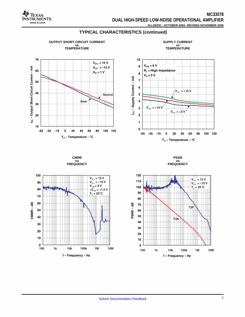
TYPICAL CHARACTERISTICS (continued)
OUTPUT SHORT-CIRCUIT CURRENT SUPPLY CURRENTvs vs
TEMPERATURE TEMPERATURE
CMRR PSSRvs vs
FREQUENCY FREQUENCY
7Submit Documentation Feedback
www.ti.com
0
5
10
15
20
25
30
-55 -35 -15 5 25 45 65 85 105 125
TA – Temperature – °C
GB
W–
Gain
Ban
dw
idth
Pro
du
ct
–M
Hz
0
5
10
15
20
25
30
5 6 7 8 9 10 11 12 13 14 15 16 17 18
VCC+/–VCC– – Supply Voltage – V
GB
W–
Gain
dB
an
dw
idth
Pro
du
ct
–M
Hz
0
5
10
15
20
25
30
1.E+01 1.E+02 1.E+03 1.E+04 1.E+05 1.E+06 1.E+07
f – Frequency – Hz
VO
–O
utp
ut
Vo
ltag
e–
V
100 1k 10k 100k 1M 10M10
V = 15 V
V = –15 V
R = 2 k
A = 1
THD < 1%T = 25°C
CC+
CC–
L
V
A
W
-20
-15
-10
-5
0
5
10
15
20
5 6 7 8 9 10 11 12 13 14 15 16 17 18
VCC+/–VCC– – Supply Voltage – V
VO
–O
utp
ut
Vo
ltag
e–
V
R = 10 kL W
R = 2 kL W
R = 10 kL W
R = 2 kL W
MC33078DUAL HIGH-SPEED LOW-NOISE OPERATIONAL AMPLIFIERSLLS633C–OCTOBER 2004–REVISED NOVEMBER 2006
TYPICAL CHARACTERISTICS (continued)
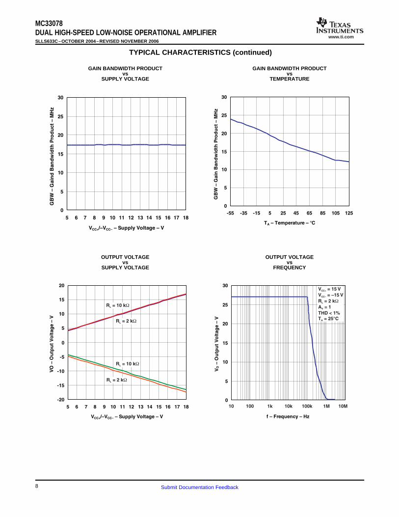
GAIN BANDWIDTH PRODUCT GAIN BANDWIDTH PRODUCTvs vs
SUPPLY VOLTAGE TEMPERATURE
OUTPUT VOLTAGE OUTPUT VOLTAGEvs vs
SUPPLY VOLTAGE FREQUENCY
8 Submit Documentation Feedback
www.ti.com
80
85
90
95
100
105
110
5 6 7 8 9 10 11 12 13 14 15 16 17 18
VCC+/–VCC– – Supply Voltage – V
AV
–O
pen
-Lo
op
Gain
–d
B
R = 2 k
f < 10 Hz
V = 2/3(V – V )
T = 25°C
L
O CC+ CC–
A
W
D
80
85
90
95
100
105
110
115
120
-55 -35 -15 5 25 45 65 85 105 125
TA – Temperature – °C
AV
–O
pen
-Lo
op
Gain
–d
B
R = 2 k
f < 10 Hz
V = 2/3(V – V )
T = 25°C
L
O CC+ CC–
A
W
D
100
110
120
130
140
150
160
170
180
190
200
1.E+01 1.E+02 1.E+03 1.E+04 1.E+05
f – Frequency – Hz
Cro
ssta
lkR
eje
cti
on
–d
B
1k 10k 100k
Drive Channel
V = 15 V
V = –15 V
R = 2 k
V = 20 V
T = 25°C
CC+
CC–
L
O PP
A
W
10 1000
5
10
15
20
25
30
35
40
45
50
1.0E+03 1.0E+04 1.0E+05 1.0E+06 1.0E+07
f – Frequency – Hz
ZO
–O
utp
ut
Imp
ed
an
ce
–
VCC+ = 15 V
VCC– = –15 V
VO = 1 Vrms
TA = 25°CW
1k 10k 100k 1M 10M
A = 1VA = 10VA = 100V
A = 1000V
MC33078DUAL HIGH-SPEED LOW-NOISE OPERATIONAL AMPLIFIER
SLLS633C–OCTOBER 2004–REVISED NOVEMBER 2006
TYPICAL CHARACTERISTICS (continued)
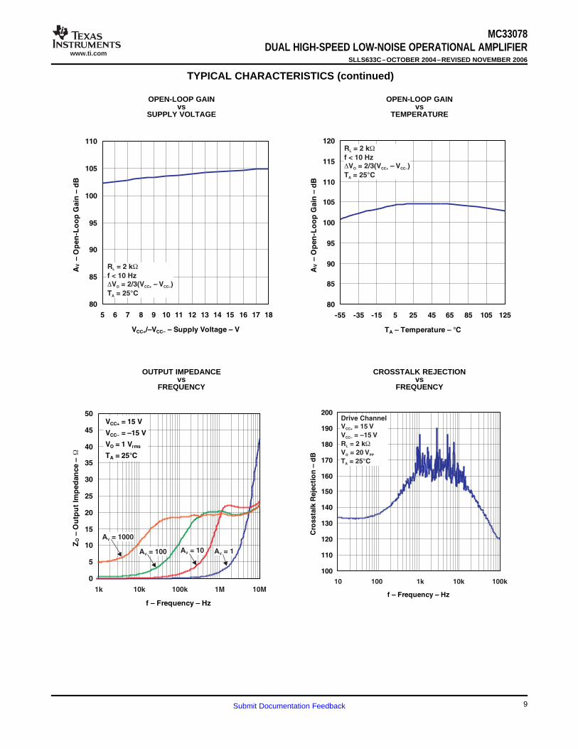
OPEN-LOOP GAIN OPEN-LOOP GAINvs vs
SUPPLY VOLTAGE TEMPERATURE
OUTPUT IMPEDANCE CROSSTALK REJECTIONvs vs
FREQUENCY FREQUENCY
9Submit Documentation Feedback
www.ti.com
0.0001
0.001
0.01
0.1
1
1.E+01 1.E+02 1.E+03 1.E+04 1.E+05
f – Frequency – Hz
TH
D–
To
talH
arm
on
icD
isto
rtio
n–
%
1k 10k 100k
V = 15 V
V = –15 V
V = 1 V
A = 1
R = 2 k
T = 25°C
CC+
CC–
O rms
V
L
A
W
10 100
0.0001
0.001
0.01
0.1
1
0 1 2 3 4 5 6 7 8 9
VO – Output Voltage – Vrms
TH
D–
To
talH
arm
on
icD
isto
rtio
n–
%
V = 15 V
V = –15 V
f = 2 kHzR = 2 k
T = 25°C
CC+
CC–
L
A
W
A = 1V
A = 10V
A = 100V
A = 1000V
2
3
4
5
6
7
8
9
10
5 6 7 8 9 10 11 12 13 14 15 16 17 18
VCC+/–VCC– – Supply Voltage – V
SR
–S
lew
Rate
–V
/µs
Falling Edge
Rising Edge
V = 2/3(V – V )
A = 1
R = 2 k
T = 25°C
D
W
IN CC+ CC–
V
L
A
2
3
4
5
6
7
8
9
10
-55 -35 -15 5 25 45 65 85 105 125
TA – Temperature – °C
SR
–S
lew
Rate
–V
/µs
V = 15 V
V = –15 VCC+
CC–
V = 20 V
A = 1
R = 2 k
D
W
IN
V
L
Falling Edge
Rising Edge
MC33078DUAL HIGH-SPEED LOW-NOISE OPERATIONAL AMPLIFIERSLLS633C–OCTOBER 2004–REVISED NOVEMBER 2006
TYPICAL CHARACTERISTICS (continued)
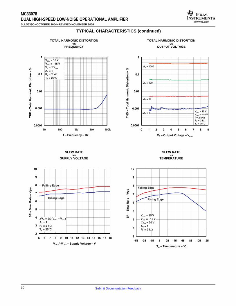
TOTAL HARMONIC DISTORTION TOTAL HARMONIC DISTORTIONvs vs
FREQUENCY OUTPUT VOLTAGE
SLEW RATE SLEW RATEvs vs
SUPPLY VOLTAGE TEMPERATURE
10 Submit Documentation Feedback
www.ti.com
0
10
20
30
40
50
60
70
80
1.E+03 1.E+04 1.E+05 1.E+06 1.E+07
f – Frequency – Hz
Gain
–d
B
-180
-135
-90
-45
0
Ph
ase
Sh
ift
–d
eg
V = 15 V
V = –15 VCC+
CC–
R = 2 k
T = 25°CL
A
W
100k 1M 10M1k 10k
Phase
Gain
0
3
6
9
12
1 10 100 1000
Cout – Output Load Capacitance – pF
Gain
Marg
in–
dB
0
10
20
30
40
50
60
70
80
Ph
ase
Marg
in–
deg
Gain,T = 125°CA
Gain,T = 25°CA
Gain,T = –55°CA
Phase,T = 125°CA
Phase,T = 25°CA
Phase,T = –55°CA
V = 15 V
V = –15 VCC+
CC–
V = 0 VO
0
10
20
30
40
50
60
70
80
90
100
10 100 1000
Cout – Output Load Capacitance – pF
Overs
ho
ot
–%
VCC+ = 15 V
VCC– = –15 V
VIN = 100 mVPP
T = 125°CA
T = 25°CA
T = –55°CA
1
10
100
10 100 1000 10000 100000
f – Frequency – Hz
Inp
ut
Vo
ltag
eN
ois
e–
nV
/rtH
z
0.1
1
10
Inp
ut
Cu
rren
tN
ois
e–
pA
/rtH
z
VCC+ = 15 V
VCC– = –15 V
TA = 25°C
Input Voltage Noise
Input Current Noise
10 100 1k 10k 100k
pA
/ÖH
z
nV
/ÖH
z
MC33078DUAL HIGH-SPEED LOW-NOISE OPERATIONAL AMPLIFIER
SLLS633C–OCTOBER 2004–REVISED NOVEMBER 2006
TYPICAL CHARACTERISTICS (continued)
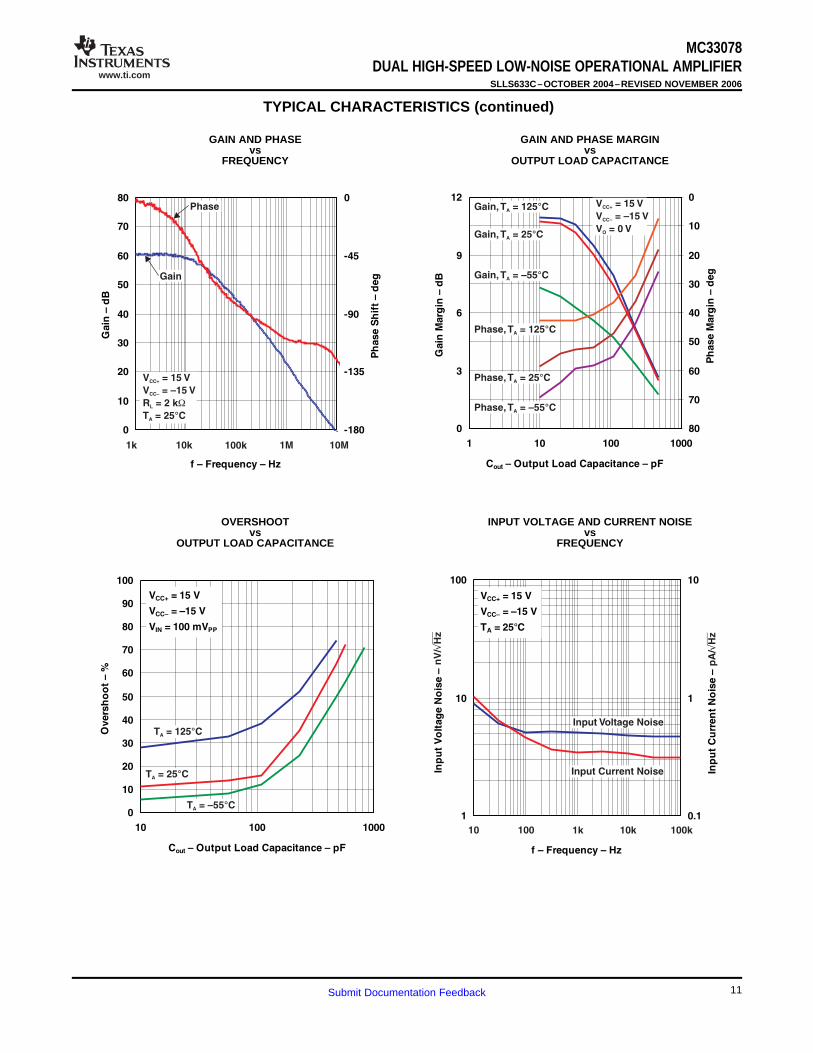
GAIN AND PHASE GAIN AND PHASE MARGINvs vs
FREQUENCY OUTPUT LOAD CAPACITANCE
OVERSHOOT INPUT VOLTAGE AND CURRENT NOISEvs vs
OUTPUT LOAD CAPACITANCE FREQUENCY
11Submit Documentation Feedback
www.ti.com
1
10
100
1000
1.E+01 1.E+02 1.E+03 1.E+04 1.E+05 1.E+06
RS – Source Resistance – è
Inp
ut
Refe
rred
No
ise
Vo
ltag
e–
nV
/rtH
z
VCC+ = 15 V
VCC– = –15 V
f = 1 Hz
TA = 25°C
W
10 100 1k 10k 100k
nV
/ÖH
z
1M0
2
4
6
8
10
12
14
16
0 1 10 100 1000 10000 100000
RSD – Differential Source Resistance – è
Gain
Marg
in–
dB
0
4
8
12
16
20
24
28
32
36
40
44
48
52
56
60
64
Ph
ase
Marg
in–
deg
VCC+ = 15 V
VCC– = –15 V
AV = 100
VO = 0 V
TA = 25°C
Phase Margin
Gain Margin
W
1k 10k 100k1000 1 10
-15
-5
5
15
25
35
45
55
-2 2 6 10 14 18 22
Time – µs
VO
–O
utp
ut
Vo
ltag
e–
V
-60
-50
-40
-30
-20
-10
0
10
VI–
Inp
ut
Vo
lta
ge
–V
V = 15 V
V = –15 V
A = 1
R = 2 k
C
T = 25°C
CC+
CC–
V
L
A
W
L = 100 pF
Input
Output
-15
-5
5
15
25
35
45
55
-2 2 6 10 14 18 22
Time – µs
VO
–O
utp
ut
Vo
ltag
e–
V
-60
-50
-40
-30
-20
-10
0
10
VI–
Inp
ut
Vo
lta
ge
–V
V = 15 V
V = –15 V
A = –1
R = 2 k
C
T = 25°C
CC+
CC–
V
L
A
W
L = 100 pF
Input
Output
MC33078DUAL HIGH-SPEED LOW-NOISE OPERATIONAL AMPLIFIERSLLS633C–OCTOBER 2004–REVISED NOVEMBER 2006
TYPICAL CHARACTERISTICS (continued)
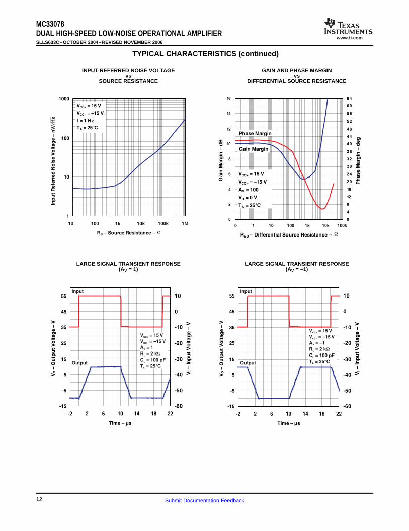
INPUT REFERRED NOISE VOLTAGE GAIN AND PHASE MARGINvs vs
SOURCE RESISTANCE DIFFERENTIAL SOURCE RESISTANCE
LARGE SIGNAL TRANSIENT RESPONSE LARGE SIGNAL TRANSIENT RESPONSE(AV = 1) (AV = –1)
12 Submit Documentation Feedback
www.ti.com
-0.2
-0.1
0
0.1
0.2
0.3
0.4
0.5
0.6
-0.5 0.0 0.5 1.0 1.5
Time – µs
VO
–O
utp
ut
Vo
ltag
e–
V
-0.6
-0.5
-0.4
-0.3
-0.2
-0.1
0.0
0.1
0.2
VI–
Inp
ut
Vo
lta
ge
–V
V = 15 V
V = –15 V
A = 1
R = 2 k
C
T = 25°C
CC+
CC–
V
L
A
W
L = 100 pF
Input
Output
-500
-400
-300
-200
-100
0
100
200
300
400
-5 -4 -3 -2 -1 0 1 2 3 4 5
Time – sIn
pu
tV
olt
ag
eN
ois
e–
nV
T3
VCC+ = 15 V
VCC– = –15 V
BW = 0.1 Hz to 10 Hz
TA = 25°C
MC33078DUAL HIGH-SPEED LOW-NOISE OPERATIONAL AMPLIFIER
SLLS633C–OCTOBER 2004–REVISED NOVEMBER 2006
TYPICAL CHARACTERISTICS (continued)
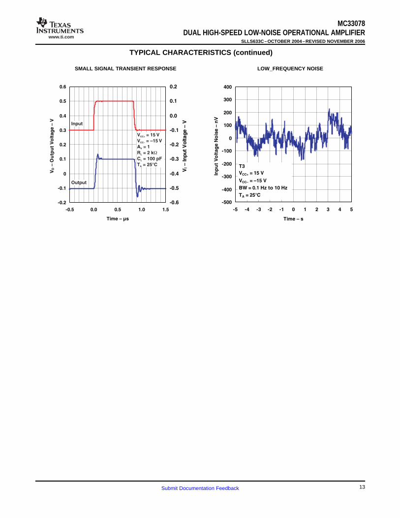
SMALL SIGNAL TRANSIENT RESPONSE LOW_FREQUENCY NOISE
13Submit Documentation Feedback
www.ti.com
APPLICATION INFORMATION
Output Characteristics
0.2
5V
per
Div
isio
n
250 ns per Division
Maximum capacitancebefore oscillation = 380 pF
250 ns per Division
0.2
5V
per
Div
isio
n
Maximum capacitancebefore oscillation = 560 pF
250 ns per Division
0.2
5V
per
Div
isio
n
Maximum capacitancebefore oscillation = 590 pF
250 ns per Division
0.2
5V
per
Div
isio
n
250 ns per Division
0.2
5V
per
Div
isio
n
250 ns per Division
0.2
5V
pe
r D
ivis
ion
5 V
–5 V
15 V
–15 V
RO
VO
R = 2 kL ΩCL
MC33078DUAL HIGH-SPEED LOW-NOISE OPERATIONAL AMPLIFIERSLLS633C–OCTOBER 2004–REVISED NOVEMBER 2006
All operating characteristics are specified with 100-pF load capacitance. The MC33078 can drive highercapacitance loads. However, as the load capacitance increases, the resulting response pole occurs at lowerfrequencies, causing ringing, peaking, or oscillation. The value of the load capacitance at which oscillationoccurs varies from lot to lot. If an application appears to be sensitive to oscillation due to load capacitance,adding a small resistance in series with the load should alleviate the problem (see Figure 2).
PULSE RESPONSE PULSE RESPONSE PULSE RESPONSE(RL = 600 Ω, CL = 380 pF) (RL = 2 kΩ, CL = 560 pF) (RL = 10 kΩ, CL = 590 pF)
PULSE RESPONSE PULSE RESPONSE PULSE RESPONSE(RO = 0 Ω, CO = 1000 pF, RL = 2 kΩ) (RO = 4 Ω, CO = 1000 pF, RL = 2 kΩ) (RO = 35 Ω, CO = 1000 pF, RL = 2 kΩ)
Figure 2. Output Characteristics
14 Submit Documentation Feedback
PACKAGE OPTION ADDENDUM
www.ti.com 10-Jun-2014
Addendum-Page 1
PACKAGING INFORMATION
Orderable Device Status(1)
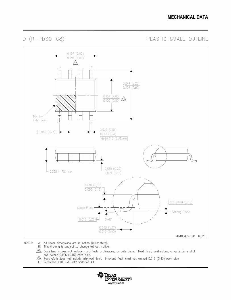
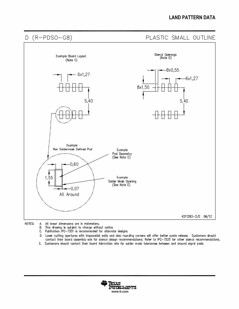
Package Type PackageDrawing
Pins PackageQty
Eco Plan(2)
Lead/Ball Finish(6)
MSL Peak Temp(3)
Op Temp (°C) Device Marking(4/5)
Samples
MC33078D ACTIVE SOIC D 8 75 Green (RoHS& no Sb/Br)
CU NIPDAU Level-1-260C-UNLIM -40 to 85 M33078
MC33078DG4 ACTIVE SOIC D 8 75 Green (RoHS& no Sb/Br)
CU NIPDAU Level-1-260C-UNLIM -40 to 85 M33078
MC33078DGKR ACTIVE VSSOP DGK 8 2500 Green (RoHS& no Sb/Br)
CU NIPDAU Level-1-260C-UNLIM -40 to 85 MYU
MC33078DGKRG4 ACTIVE VSSOP DGK 8 2500 Green (RoHS& no Sb/Br)
CU NIPDAU Level-1-260C-UNLIM -40 to 85 MYU
MC33078DGKT ACTIVE VSSOP DGK 8 250 Green (RoHS& no Sb/Br)
CU NIPDAU Level-1-260C-UNLIM -40 to 85 MYU
MC33078DR ACTIVE SOIC D 8 2500 Green (RoHS& no Sb/Br)
CU NIPDAU Level-1-260C-UNLIM -40 to 85 M33078
MC33078DRE4 ACTIVE SOIC D 8 2500 Green (RoHS& no Sb/Br)
CU NIPDAU Level-1-260C-UNLIM -40 to 85 M33078
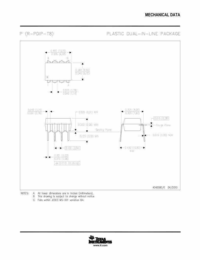
MC33078P ACTIVE PDIP P 8 50 Pb-Free(RoHS)
CU NIPDAU N / A for Pkg Type -40 to 85 MC33078P
(1) The marketing status values are defined as follows:ACTIVE: Product device recommended for new designs.LIFEBUY: TI has announced that the device will be discontinued, and a lifetime-buy period is in effect.NRND: Not recommended for new designs. Device is in production to support existing customers, but TI does not recommend using this part in a new design.PREVIEW: Device has been announced but is not in production. Samples may or may not be available.OBSOLETE: TI has discontinued the production of the device.
(2) Eco Plan - The planned eco-friendly classification: Pb-Free (RoHS), Pb-Free (RoHS Exempt), or Green (RoHS & no Sb/Br) - please check http://www.ti.com/productcontent for the latest availabilityinformation and additional product content details.TBD: The Pb-Free/Green conversion plan has not been defined.Pb-Free (RoHS): TI's terms "Lead-Free" or "Pb-Free" mean semiconductor products that are compatible with the current RoHS requirements for all 6 substances, including the requirement thatlead not exceed 0.1% by weight in homogeneous materials. Where designed to be soldered at high temperatures, TI Pb-Free products are suitable for use in specified lead-free processes.Pb-Free (RoHS Exempt): This component has a RoHS exemption for either 1) lead-based flip-chip solder bumps used between the die and package, or 2) lead-based die adhesive used betweenthe die and leadframe. The component is otherwise considered Pb-Free (RoHS compatible) as defined above.Green (RoHS & no Sb/Br): TI defines "Green" to mean Pb-Free (RoHS compatible), and free of Bromine (Br) and Antimony (Sb) based flame retardants (Br or Sb do not exceed 0.1% by weightin homogeneous material)
(3) MSL, Peak Temp. - The Moisture Sensitivity Level rating according to the JEDEC industry standard classifications, and peak solder temperature.
PACKAGE OPTION ADDENDUM
www.ti.com 10-Jun-2014
Addendum-Page 2
(4) There may be additional marking, which relates to the logo, the lot trace code information, or the environmental category on the device.
(5) Multiple Device Markings will be inside parentheses. Only one Device Marking contained in parentheses and separated by a "~" will appear on a device. If a line is indented then it is a continuationof the previous line and the two combined represent the entire Device Marking for that device.
(6) Lead/Ball Finish - Orderable Devices may have multiple material finish options. Finish options are separated by a vertical ruled line. Lead/Ball Finish values may wrap to two lines if the finishvalue exceeds the maximum column width.
Important Information and Disclaimer:The information provided on this page represents TI's knowledge and belief as of the date that it is provided. TI bases its knowledge and belief on informationprovided by third parties, and makes no representation or warranty as to the accuracy of such information. Efforts are underway to better integrate information from third parties. TI has taken andcontinues to take reasonable steps to provide representative and accurate information but may not have conducted destructive testing or chemical analysis on incoming materials and chemicals.TI and TI suppliers consider certain information to be proprietary, and thus CAS numbers and other limited information may not be available for release.
In no event shall TI's liability arising out of such information exceed the total purchase price of the TI part(s) at issue in this document sold by TI to Customer on an annual basis.
OTHER QUALIFIED VERSIONS OF MC33078 :
• Enhanced Product: MC33078-EP
NOTE: Qualified Version Definitions:
• Enhanced Product - Supports Defense, Aerospace and Medical Applications
TAPE AND REEL INFORMATION
*All dimensions are nominal
Device PackageType
PackageDrawing
Pins SPQ ReelDiameter
(mm)
ReelWidth
W1 (mm)
A0(mm)
B0(mm)
K0(mm)
P1(mm)
W(mm)
Pin1Quadrant
MC33078DGKR VSSOP DGK 8 2500 330.0 12.4 5.3 3.3 1.3 8.0 12.0 Q1
MC33078DGKT VSSOP DGK 8 250 180.0 12.4 5.3 3.3 1.3 8.0 12.0 Q1
MC33078DR SOIC D 8 2500 330.0 12.4 6.4 5.2 2.1 8.0 12.0 Q1
MC33078DR SOIC D 8 2500 330.0 12.4 6.4 5.2 2.1 8.0 12.0 Q1
PACKAGE MATERIALS INFORMATION
www.ti.com 3-Aug-2017
Pack Materials-Page 1
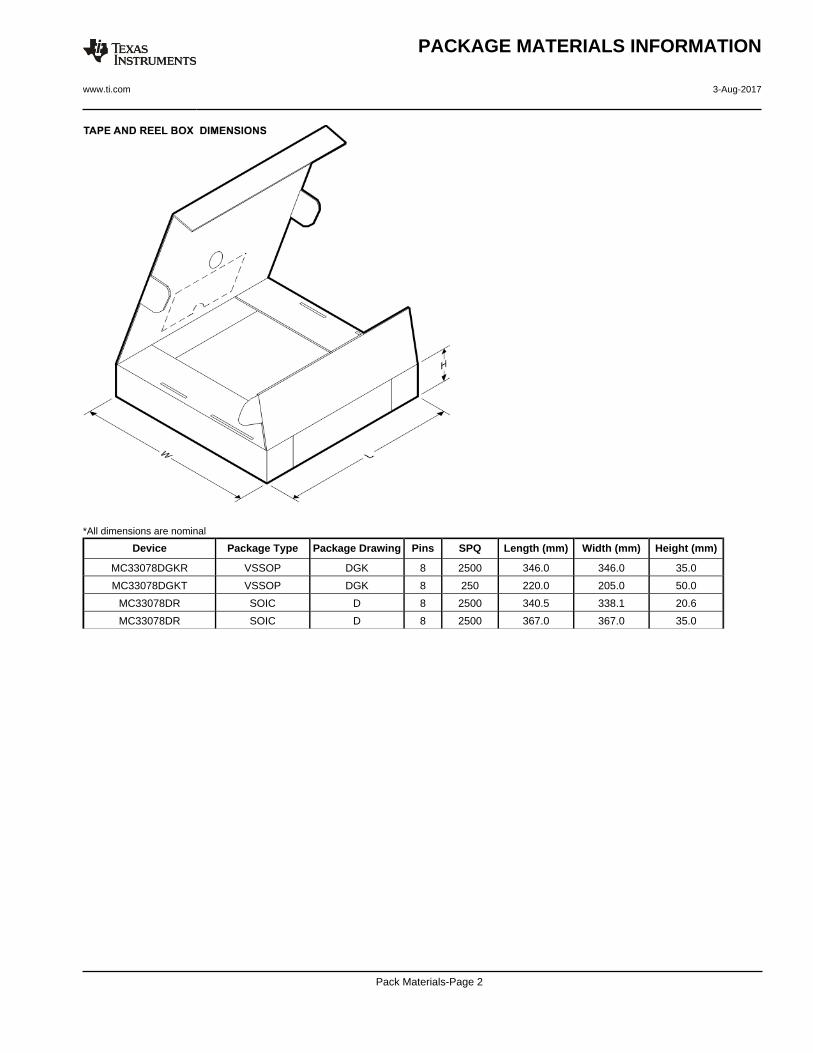
*All dimensions are nominal
Device Package Type Package Drawing Pins SPQ Length (mm) Width (mm) Height (mm)
MC33078DGKR VSSOP DGK 8 2500 346.0 346.0 35.0
MC33078DGKT VSSOP DGK 8 250 220.0 205.0 50.0
MC33078DR SOIC D 8 2500 340.5 338.1 20.6
MC33078DR SOIC D 8 2500 367.0 367.0 35.0
PACKAGE MATERIALS INFORMATION
www.ti.com 3-Aug-2017
Pack Materials-Page 2
IMPORTANT NOTICE
Texas Instruments Incorporated (TI) reserves the right to make corrections, enhancements, improvements and other changes to itssemiconductor products and services per JESD46, latest issue, and to discontinue any product or service per JESD48, latest issue. Buyersshould obtain the latest relevant information before placing orders and should verify that such information is current and complete.TI’s published terms of sale for semiconductor products (http://www.ti.com/sc/docs/stdterms.htm) apply to the sale of packaged integratedcircuit products that TI has qualified and released to market. Additional terms may apply to the use or sale of other types of TI products andservices.Reproduction of significant portions of TI information in TI data sheets is permissible only if reproduction is without alteration and isaccompanied by all associated warranties, conditions, limitations, and notices. TI is not responsible or liable for such reproduceddocumentation. Information of third parties may be subject to additional restrictions. Resale of TI products or services with statementsdifferent from or beyond the parameters stated by TI for that product or service voids all express and any implied warranties for theassociated TI product or service and is an unfair and deceptive business practice. TI is not responsible or liable for any such statements.Buyers and others who are developing systems that incorporate TI products (collectively, “Designers”) understand and agree that Designersremain responsible for using their independent analysis, evaluation and judgment in designing their applications and that Designers havefull and exclusive responsibility to assure the safety of Designers' applications and compliance of their applications (and of all TI productsused in or for Designers’ applications) with all applicable regulations, laws and other applicable requirements. Designer represents that, withrespect to their applications, Designer has all the necessary expertise to create and implement safeguards that (1) anticipate dangerousconsequences of failures, (2) monitor failures and their consequences, and (3) lessen the likelihood of failures that might cause harm andtake appropriate actions. Designer agrees that prior to using or distributing any applications that include TI products, Designer willthoroughly test such applications and the functionality of such TI products as used in such applications.TI’s provision of technical, application or other design advice, quality characterization, reliability data or other services or information,including, but not limited to, reference designs and materials relating to evaluation modules, (collectively, “TI Resources”) are intended toassist designers who are developing applications that incorporate TI products; by downloading, accessing or using TI Resources in anyway, Designer (individually or, if Designer is acting on behalf of a company, Designer’s company) agrees to use any particular TI Resourcesolely for this purpose and subject to the terms of this Notice.TI’s provision of TI Resources does not expand or otherwise alter TI’s applicable published warranties or warranty disclaimers for TIproducts, and no additional obligations or liabilities arise from TI providing such TI Resources. TI reserves the right to make corrections,enhancements, improvements and other changes to its TI Resources. TI has not conducted any testing other than that specificallydescribed in the published documentation for a particular TI Resource.Designer is authorized to use, copy and modify any individual TI Resource only in connection with the development of applications thatinclude the TI product(s) identified in such TI Resource. NO OTHER LICENSE, EXPRESS OR IMPLIED, BY ESTOPPEL OR OTHERWISETO ANY OTHER TI INTELLECTUAL PROPERTY RIGHT, AND NO LICENSE TO ANY TECHNOLOGY OR INTELLECTUAL PROPERTYRIGHT OF TI OR ANY THIRD PARTY IS GRANTED HEREIN, including but not limited to any patent right, copyright, mask work right, orother intellectual property right relating to any combination, machine, or process in which TI products or services are used. Informationregarding or referencing third-party products or services does not constitute a license to use such products or services, or a warranty orendorsement thereof. Use of TI Resources may require a license from a third party under the patents or other intellectual property of thethird party, or a license from TI under the patents or other intellectual property of TI.TI RESOURCES ARE PROVIDED “AS IS” AND WITH ALL FAULTS. TI DISCLAIMS ALL OTHER WARRANTIES ORREPRESENTATIONS, EXPRESS OR IMPLIED, REGARDING RESOURCES OR USE THEREOF, INCLUDING BUT NOT LIMITED TOACCURACY OR COMPLETENESS, TITLE, ANY EPIDEMIC FAILURE WARRANTY AND ANY IMPLIED WARRANTIES OFMERCHANTABILITY, FITNESS FOR A PARTICULAR PURPOSE, AND NON-INFRINGEMENT OF ANY THIRD PARTY INTELLECTUALPROPERTY RIGHTS. TI SHALL NOT BE LIABLE FOR AND SHALL NOT DEFEND OR INDEMNIFY DESIGNER AGAINST ANY CLAIM,INCLUDING BUT NOT LIMITED TO ANY INFRINGEMENT CLAIM THAT RELATES TO OR IS BASED ON ANY COMBINATION OFPRODUCTS EVEN IF DESCRIBED IN TI RESOURCES OR OTHERWISE. IN NO EVENT SHALL TI BE LIABLE FOR ANY ACTUAL,DIRECT, SPECIAL, COLLATERAL, INDIRECT, PUNITIVE, INCIDENTAL, CONSEQUENTIAL OR EXEMPLARY DAMAGES INCONNECTION WITH OR ARISING OUT OF TI RESOURCES OR USE THEREOF, AND REGARDLESS OF WHETHER TI HAS BEENADVISED OF THE POSSIBILITY OF SUCH DAMAGES.Unless TI has explicitly designated an individual product as meeting the requirements of a particular industry standard (e.g., ISO/TS 16949and ISO 26262), TI is not responsible for any failure to meet such industry standard requirements.Where TI specifically promotes products as facilitating functional safety or as compliant with industry functional safety standards, suchproducts are intended to help enable customers to design and create their own applications that meet applicable functional safety standardsand requirements. Using products in an application does not by itself establish any safety features in the application. Designers mustensure compliance with safety-related requirements and standards applicable to their applications. Designer may not use any TI products inlife-critical medical equipment unless authorized officers of the parties have executed a special contract specifically governing such use.Life-critical medical equipment is medical equipment where failure of such equipment would cause serious bodily injury or death (e.g., lifesupport, pacemakers, defibrillators, heart pumps, neurostimulators, and implantables). Such equipment includes, without limitation, allmedical devices identified by the U.S. Food and Drug Administration as Class III devices and equivalent classifications outside the U.S.TI may expressly designate certain products as completing a particular qualification (e.g., Q100, Military Grade, or Enhanced Product).Designers agree that it has the necessary expertise to select the product with the appropriate qualification designation for their applicationsand that proper product selection is at Designers’ own risk. Designers are solely responsible for compliance with all legal and regulatoryrequirements in connection with such selection.Designer will fully indemnify TI and its representatives against any damages, costs, losses, and/or liabilities arising out of Designer’s non-compliance with the terms and provisions of this Notice.
Mailing Address: Texas Instruments, Post Office Box 655303, Dallas, Texas 75265Copyright © 2017, Texas Instruments Incorporated