Dual Auto-Zeroed Operational Amplifiers · • Instrumentation ... the world's first complete...
12
2002 Microchip Technology Inc. DS21482B-page 1 TC913A/TC913B Features • First Monolithic Dual Auto-Zeroed Operational Amplifier • Chopper Amplifier Performance Without External Capacitors -V OS : 15µV Max -V OS : Drift; 0.15µV/°C Max - Saves Cost of External Capacitors • SOIC Packages Available • High DC Gain; 120dB • Low Supply Current; 650µA • Low Input Voltage Noise - 0.65µV P-P (0.1Hz to 10Hz) • Wide Common Mode Voltage Range -V SS to V DD - 2V • High Common Mode Rejection; 116dB • Dual or Single Supply Operation: - ±3.3V to ±8.3V - +6.5V to +16V • Excellent AC Operating Characteristics - Slew Rate; 2.5V/µsec - Unity-Gain Bandwidth; 1.5MHz • Pin Compatible with LM358, OP-14, MC1458, ICL7621, TL082, TLC322 Applications • Instrumentation • Medical Instrumentation • Embedded Control • Temperature Sensor Amplifier • Strain Gage Amplifier Device Selection Table Package Type General Description The TC913 is the world's first complete monolithic, dual auto-zeroed operational amplifier. The TC913 sets a new standard for low power, precision dual-operational amplifiers. Chopper-stabilized or auto-zeroed amplifi- ers offer low offset voltage errors by periodically sam- pling offset error, and storing correction voltages on capacitors. Previous single amplifier designs required two user-supplied, external 0.1µF error storage correc- tion capacitors — much too large for on-chip integra- tion. The unique TC913 architecture requires smaller capacitors, making on-chip integration possible. Microvolt offset levels are achieved and external capacitors are not required. The TC913 system benefits are apparent when con- trasted with a TC7650 chopper amplifier circuit imple- mentation. A single TC913 replaces two TC7650's and four capacitors. Five components and assembly steps are eliminated. The TC913 pinout matches many popular dual-opera- tional amplifiers: OP-04, TLC322, LM358, and ICL7621 are typical examples. In many applications, operating from dual 5V power supplies or single supplies, the TC913 offers superior electrical performance, and can be a functional drop-in replacement; printed circuit board rework is not necessary. The TC913's low offset voltage error eliminates offset voltage trim potentiometers often needed with bipolar and low accuracy CMOS operational amplifiers. The TC913 takes full advantage of Microchip's proprietary CMOS technology. Unity gain bandwidth is 1.5MHz and slew rate is 2.5V/µsec. Part Number Package Temp. Range Offset Voltage TC913ACOA 8-Pin SOIC 0°C to +70°C 15µV TC913ACPA 8-Pin PDIP 0°C to +70°C 15µV TC913BCOA 8-Pin SOIC 0°C to +70°C 30µV TC913BCPA 8-Pin PDIP 0°C to +70°C 30µV 1 2 3 4 6 5 -IN B 7 8 OUT A -IN A +IN A V SS V SS V DD V DD +IN B PDIP SOIC TC913ACPA TC913BCPA TC913ACOA TC913BCOA OUT B + - - + A B 1 2 3 4 6 5 -IN B 7 8 OUT A -IN A +IN A +IN B OUT B + - - + A B Dual Auto-Zeroed Operational Amplifiers
-
Upload
trinhquynh -
Category
Documents
-
view
221 -
download
0
Transcript of Dual Auto-Zeroed Operational Amplifiers · • Instrumentation ... the world's first complete...

2002 Microchip Technology Inc. DS21482B-page 1
TC913A/TC913B
Features
• First Monolithic Dual Auto-ZeroedOperational Amplifier
• Chopper Amplifier Performance Without ExternalCapacitors
- VOS: 15µV Max
- VOS: Drift; 0.15µV/°C Max
- Saves Cost of External Capacitors
• SOIC Packages Available
• High DC Gain; 120dB
• Low Supply Current; 650µA
• Low Input Voltage Noise
- 0.65µVP-P (0.1Hz to 10Hz)
• Wide Common Mode Voltage Range
- VSS to VDD - 2V
• High Common Mode Rejection; 116dB
• Dual or Single Supply Operation:
- ±3.3V to ±8.3V
- +6.5V to +16V
• Excellent AC Operating Characteristics
- Slew Rate; 2.5V/µsec
- Unity-Gain Bandwidth; 1.5MHz
• Pin Compatible with LM358, OP-14, MC1458,ICL7621, TL082, TLC322
Applications
• Instrumentation
• Medical Instrumentation
• Embedded Control
• Temperature Sensor Amplifier
• Strain Gage Amplifier
Device Selection Table
Package Type
General Description
The TC913 is the world's first complete monolithic, dualauto-zeroed operational amplifier. The TC913 sets anew standard for low power, precision dual-operationalamplifiers. Chopper-stabilized or auto-zeroed amplifi-ers offer low offset voltage errors by periodically sam-pling offset error, and storing correction voltages oncapacitors. Previous single amplifier designs requiredtwo user-supplied, external 0.1µF error storage correc-tion capacitors — much too large for on-chip integra-tion. The unique TC913 architecture requires smallercapacitors, making on-chip integration possible.Microvolt offset levels are achieved and externalcapacitors are not required.
The TC913 system benefits are apparent when con-trasted with a TC7650 chopper amplifier circuit imple-mentation. A single TC913 replaces two TC7650's andfour capacitors. Five components and assembly stepsare eliminated.
The TC913 pinout matches many popular dual-opera-tional amplifiers: OP-04, TLC322, LM358, and ICL7621are typical examples. In many applications, operatingfrom dual 5V power supplies or single supplies, theTC913 offers superior electrical performance, and canbe a functional drop-in replacement; printed circuitboard rework is not necessary. The TC913's low offsetvoltage error eliminates offset voltage trimpotentiometers often needed with bipolar and lowaccuracy CMOS operational amplifiers.
The TC913 takes full advantage of Microchip'sproprietary CMOS technology. Unity gain bandwidth is1.5MHz and slew rate is 2.5V/µsec.
Part Number PackageTemp.Range
OffsetVoltage
TC913ACOA 8-Pin SOIC 0°C to+70°C
15µV
TC913ACPA 8-Pin PDIP 0°C to+70°C
15µV
TC913BCOA 8-Pin SOIC 0°C to+70°C
30µV
TC913BCPA 8-Pin PDIP 0°C to+70°C
30µV
1
2
3
4
6
5
-IN B
7
8OUT A
-IN A
+IN A
VSS
VSS
VDD
VDD
+IN B
PDIP
SOIC
TC913ACPATC913BCPA
TC913ACOATC913BCOA
OUT B+-
-+
AB
1
2
3
4
6
5
-IN B
7
8OUT A
-IN A
+IN A
+IN B
OUT B+-
-+
AB
Dual Auto-Zeroed Operational Amplifiers

TC913A/TC913B
DS21482B-page 2 2002 Microchip Technology Inc.
Functional Block Diagram
-
++
-
TC913
A
4 8
B*
A
B
*NOTE: Internal capacitors. No external capacitors required.
Main Amplifier
Low ImpedanceOutput Buffer
InternalOscillator
(fOSC 200Hz)
+
–
-Input A -Input B
1 of 2 Amplifier Shown
Output A
26
+Input A+Input B 3
5
Output B7
1
*
VDDVSS
VOS Correction Amplifier

2002 Microchip Technology Inc. DS21482B-page 3
TC913A/TC913B
1.0 ELECTRICALCHARACTERISTICS
Absolute Maximum Ratings*
Total Supply Voltage (VDD to VSS) .......................+18V
Input Voltage ...................... (VDD +0.3V) to (VSS-0.3V)
Current Into Any Pin............................................ 10mAWhile Operating ..........................................100µA
Package Power Dissipation (TA – 70°C)Plastic DIP ................................................ 730mWPlastic SOIC ............................................. 470mW
Operating Temperature RangeC Device .......................................... 0°C to +70°C
Storage Temperature Range.............. -65°C to +150°C
*Stresses above those listed under "Absolute MaximumRatings" may cause permanent damage to the device. Theseare stress ratings only and functional operation of the deviceat these or any other conditions above those indicated in theoperation sections of the specifications is not implied. Expo-sure to Absolute Maximum Rating conditions for extendedperiods may affect device reliability.
TC913A AND TC913B ELECTRICAL SPECIFICATIONS
Electrical Characteristics: VS = ±5V, TA = +25°C, unless otherwise indicated.
TC913A TC913B
Symbol Parameter Min Typ Max Min Typ Max Unit Test Conditions
VOS Input OffsetVoltage
— 5 15 — 15 30 µV TA = +25°C
TCVOS Average Temp.Coefficient ofInput OffsetVoltage
——
0.050.05
0.150.15
——
0.10.1
0.250.25
µV/°CµV/°C
0°C ≤ TA ≤ +70°C-25°C ≤ TA ≤ +85°C(Note 1)
IB Average InputBias Current
———
———
9034
———
———
12046
pAnAnA
TA = +25°C0°C ≤ TA ≤ +70°C-25°C ≤ TA ≤ +85°
IOS Average InputOffset Current
——
5—
201
——
10—
401
pAnA
TA = +25°CTA = +85°C
eN Input VoltageNoise
——
0.611
——
——
0.611
——
µVP-PµVP-P
0.1 to 1 Hz, RS ≤ 100Ω0.1 to 10 Hz, RS ≤ 100Ω
CMRR Common ModeRejection Ratio
110 116 — 100 110 — dB VSS ≤ VCM ≤ VDD - 2.2
CMVR Common ModeVoltage Range
VSS — VDD - 2 VSS — VDD - 2 V
AOL Open-LoopVoltage Gain
115 120 — 110 120 — dB RL = 10 kΩ, VOUT = ±4V
VOUT Output VoltageSwing
VSS + 0.3 — VDD - 0.9 VSS + 0.3 — VDD -0.9 V RL = 10 kΩ
BW Closed LoopBandwidth
— 1.5 — — 1.5 — MHz Closed Loop Gain = +1
SR Slew Rate — 2.5 — — 2.5 — V/µsec RL = 10 kΩ, CL = 50 pF
PSRR Power SupplyRejection Ratio
110 — — 100 — — dB ±3.3V to ±5.5V
VS OperatingSupply VoltageRange
±3.36.5
——
±8.316
±3.36.5
——
±8.316
VV
Split SupplySingle Supply
IS QuiescentSupply Current
— 0.65 0.85 — — 1.1 mA VS = ±5V
Note 1: Characterized; not 100% tested.
TC913A/TC913B
DS21482B-page 4 2002 Microchip Technology Inc.
2.0 PIN DESCRIPTIONS
The descriptions of the pins are listed in Table 2-1.
TABLE 2-1: PIN FUNCTION TABLE
Pin No.(8-Pin PDIP)(8-Pin SOIC)
Symbol Description
1 OUT A Output
2 -IN A Inverting Input
3 +IN A Non-inverting Input
4 VSS Negative Power Supply
5 +IN B Non-inverting Input
6 -IN B Inverting Input
7 OUT B Output
8 VDD Positive Power Supply

2002 Microchip Technology Inc. DS21482B-page 5
TC913A/TC913B
3.0 DETAILED DESCRIPTION
3.1 Theory of Operation
Each of the TC913's two Op Amps actually consists oftwo amplifiers. A main amplifier is always connectedfrom the input to the output. A separate nulling amplifieralternately nulls its own offset and then the offset of theamplifier. Since each amplifier is continuously beingnulled, offset voltage drift with time, temperature andpower supply variations is greatly reduced.
All nulling circuitry is internal and the nulling operationis transparent to the user. Offset nulling voltages arestored on two internal capacitors. An internal oscillatorand control logic, shared by the TC913's two amplifiers,control the nulling process.
3.2 Pin Compatibility
The TC913 pinout is compatible with OP-14, LM358,MC1458, LT1013, TLC322, and similar dual Op Amps.In many circuits operating from single or ±5V supplies,the TC913 is a drop-in replacement offering DCperformance rivaling that of the best single Op Amps.
The TC913's amplifiers include a low-impedance classAB output buffer. Some previous CMOS chopperamplifiers used a high impedance output stage whichmade open-loop gain dependent on load resistance.The TC913's open-loop gain is not dependent on loadresistance.
3.3 Overload Recovery
The TC913 recovers quickly from output saturation.Typical recovery time from positive output saturation is20 msec. Negative output saturation recovery time istypically 5 msec.
3.4 Avoiding Latchup
Junction-isolated CMOS circuits inherently contain aparasitic p-n-p-n transistor circuit. Voltages exceedingthe supplies by 0.3V should not be applied to thedevice pins. Larger voltages can turn the p-n-p-ndevice on, causing excessive device power supplycurrent and power dissipation. The TC913's powersupplies should be established at the same time orbefore input signals are applied. If this is not possible,input current should be limited to 0.1mA to avoidtriggering the p-n-p-n structure.

TC913A/TC913B
DS21482B-page 6 2002 Microchip Technology Inc.
4.0 TYPICAL CHARACTERISTICS
Note: The graphs and tables provided following this note are a statistical summary based on a limited number ofsamples and are provided for informational purposes only. The performance characteristics listed herein arenot tested or guaranteed. In some graphs or tables, the data presented may be outside the specifiedoperating range (e.g., outside specified power supply range) and therefore outside the warranted range.
HORIZONTAL SCALE = 20 msec/DIV
Positive Overload Recovery Time
0V
OUTPUT =2 V/DIV
INPUT INPUT
GAIN = –20
35
INP
UT
OF
FS
ET
VO
LT
AG
E (
µV
)
-6INPUT COMMON MODE VOLTAGE (V)
Input Offset Voltage vs. Common Mode Voltage
30
25
20
15
10
5
0-5 -4 -3 -2 -1 0 1 2 3 4
VA = ±5V
TA = +25˚C
SU
PP
LY
CU
RR
EN
T (
µA
)
± SUPPLY VOLTAGE (V)
Supply Current vs. ± Supply Voltage
HORIZONTAL SCALE = 20 msec/DIV
Negative Overload Recovery Time
RL = 10 k
TA = +25˚C
Ω
INPUT 0V
OUTPUT= 2 V/DIV
50
CL
OS
ED
-LO
OP
GA
IN (
dB
)
10kFREQUENCY (Hz)
Gain and Phase vs. Frequency
40
30
20
10
0
-10
-20
-30
-40100k 1M 10M
PHASE
GAIN
VS = ±5V
TA = +25˚CRL = 10 kΩ
225
PH
AS
E (
deg
)
180
135
90
45
0
-45
-90
-135
-180
± O
UT
PU
T V
OL
TA
GE
(V
)
100LOAD RESISTANCE (Ω)
Output Voltage Swing vs. Load Resistance
5.0VS = ±5VTA = +25˚C
-SWING
+SWING4.2
3.4
2.6
1.8
1.01k 10k 100k 1M
1200
1000
800
600
400
200
02 3 54 6 7 8
TA = +25˚C
Gain = –20

2002 Microchip Technology Inc. DS21482B-page 7
TC913A/TC913B
5.0 PACKAGING INFORMATION
5.1 Package Marking Information
Package marking data not available at this time.
5.2 Taping Form
Component Taping Orientation for 8-Pin SOIC (Narrow) Devices
Package Carrier Width (W) Pitch (P) Part Per Full Reel Reel Size
8-Pin SOIC (N) 12 mm 8 mm 2500 13 in
Carrier Tape, Number of Components Per Reel and Reel Size
Standard Reel Component Orientationfor TR Suffix Device
PIN 1
User Direction of Feed
P
W
TC913A/TC913B
DS21482B-page 8 2002 Microchip Technology Inc.
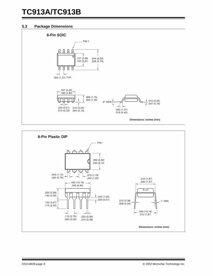
5.3 Package Dimensions
.050 (1.27) TYP.
8° MAX.
PIN 1
.244 (6.20)
.228 (5.79).157 (3.99).150 (3.81)
.197 (5.00)
.189 (4.80)
.020 (0.51)
.013 (0.33).010 (0.25).004 (0.10)
.069 (1.75)
.053 (1.35) .010 (0.25).007 (0.18)
.050 (1.27)
.016 (0.40)
.
8-Pin SOIC
Dimensions: inches (mm)
3° MIN.
PIN 1
.260 (6.60)
.240 (6.10)
.045 (1.14)
.030 (0.76).070 (1.78).040 (1.02)
.400 (10.16).348 (8.84)
.200 (5.08)
.140 (3.56)
.150 (3.81)
.115 (2.92)
.110 (2.79)
.090 (2.29).022 (0.56).015 (0.38)
.040 (1.02)
.020 (0.51) .015 (0.38).008 (0.20)
.310 (7.87)
.290 (7.37)
.400 (10.16).310 (7.87)
8-Pin Plastic DIP
Dimensions: inches (mm)

2002 Microchip Technology Inc. DS21482B-page 9
TC913A/TC913B
SALES AND SUPPORT
Data SheetsProducts supported by a preliminary Data Sheet may have an errata sheet describing minor operational differences and recom-mended workarounds. To determine if an errata sheet exists for a particular device, please contact one of the following:
1. Your local Microchip sales office2. The Microchip Corporate Literature Center U.S. FAX: (480) 792-72773. The Microchip Worldwide Site (www.microchip.com)
Please specify which device, revision of silicon and Data Sheet (include Literature #) you are using.
New Customer Notification SystemRegister on our web site (www.microchip.com/cn) to receive the most current information on our products.

TC913A/TC913B
DS21482B-page 10 2002 Microchip Technology Inc.
NOTES:
2002 Microchip Technology Inc. DS21482B-page 11
TC913A/TC913B
Information contained in this publication regarding deviceapplications and the like is intended through suggestion onlyand may be superseded by updates. It is your responsibility toensure that your application meets with your specifications.No representation or warranty is given and no liability isassumed by Microchip Technology Incorporated with respectto the accuracy or use of such information, or infringement ofpatents or other intellectual property rights arising from suchuse or otherwise. Use of Microchip’s products as critical com-ponents in life support systems is not authorized except withexpress written approval by Microchip. No licenses are con-veyed, implicitly or otherwise, under any intellectual propertyrights.
Trademarks
The Microchip name and logo, the Microchip logo, FilterLab,KEELOQ, microID, MPLAB, PIC, PICmicro, PICMASTER,PICSTART, PRO MATE, SEEVAL and The Embedded ControlSolutions Company are registered trademarks of Microchip Tech-nology Incorporated in the U.S.A. and other countries.
dsPIC, ECONOMONITOR, FanSense, FlexROM, fuzzyLAB,In-Circuit Serial Programming, ICSP, ICEPIC, microPort,Migratable Memory, MPASM, MPLIB, MPLINK, MPSIM,MXDEV, PICC, PICDEM, PICDEM.net, rfPIC, Select Modeand Total Endurance are trademarks of Microchip TechnologyIncorporated in the U.S.A.
Serialized Quick Turn Programming (SQTP) is a service markof Microchip Technology Incorporated in the U.S.A.
All other trademarks mentioned herein are property of theirrespective companies.
© 2002, Microchip Technology Incorporated, Printed in theU.S.A., All Rights Reserved.
Printed on recycled paper.
Microchip received QS-9000 quality systemcertification for its worldwide headquarters,design and wafer fabrication facilities inChandler and Tempe, Arizona in July 1999and Mountain View, California in March 2002.The Company’s quality system processes andprocedures are QS-9000 compliant for itsPICmicro® 8-bit MCUs, KEELOQ® code hoppingdevices, Serial EEPROMs, microperipherals,non-volatile memory and analog products. Inaddition, Microchip’s quality system for thedesign and manufacture of developmentsystems is ISO 9001 certified.
DS21482B-page 12 2002 Microchip Technology Inc.
AMERICASCorporate Office2355 West Chandler Blvd.Chandler, AZ 85224-6199Tel: 480-792-7200 Fax: 480-792-7277Technical Support: 480-792-7627Web Address: http://www.microchip.comRocky Mountain2355 West Chandler Blvd.Chandler, AZ 85224-6199Tel: 480-792-7966 Fax: 480-792-7456
Atlanta500 Sugar Mill Road, Suite 200BAtlanta, GA 30350Tel: 770-640-0034 Fax: 770-640-0307Boston2 Lan Drive, Suite 120Westford, MA 01886Tel: 978-692-3848 Fax: 978-692-3821Chicago333 Pierce Road, Suite 180Itasca, IL 60143Tel: 630-285-0071 Fax: 630-285-0075Dallas4570 Westgrove Drive, Suite 160Addison, TX 75001Tel: 972-818-7423 Fax: 972-818-2924DetroitTri-Atria Office Building32255 Northwestern Highway, Suite 190Farmington Hills, MI 48334Tel: 248-538-2250 Fax: 248-538-2260Kokomo2767 S. Albright RoadKokomo, Indiana 46902Tel: 765-864-8360 Fax: 765-864-8387Los Angeles18201 Von Karman, Suite 1090Irvine, CA 92612Tel: 949-263-1888 Fax: 949-263-1338New York150 Motor Parkway, Suite 202Hauppauge, NY 11788Tel: 631-273-5305 Fax: 631-273-5335San JoseMicrochip Technology Inc.2107 North First Street, Suite 590San Jose, CA 95131Tel: 408-436-7950 Fax: 408-436-7955Toronto6285 Northam Drive, Suite 108Mississauga, Ontario L4V 1X5, CanadaTel: 905-673-0699 Fax: 905-673-6509
ASIA/PACIFICAustraliaMicrochip Technology Australia Pty LtdSuite 22, 41 Rawson StreetEpping 2121, NSWAustraliaTel: 61-2-9868-6733 Fax: 61-2-9868-6755China - BeijingMicrochip Technology Consulting (Shanghai)Co., Ltd., Beijing Liaison OfficeUnit 915Bei Hai Wan Tai Bldg.No. 6 Chaoyangmen BeidajieBeijing, 100027, No. ChinaTel: 86-10-85282100 Fax: 86-10-85282104China - ChengduMicrochip Technology Consulting (Shanghai)Co., Ltd., Chengdu Liaison OfficeRm. 2401, 24th Floor,Ming Xing Financial TowerNo. 88 TIDU StreetChengdu 610016, ChinaTel: 86-28-86766200 Fax: 86-28-86766599China - FuzhouMicrochip Technology Consulting (Shanghai)Co., Ltd., Fuzhou Liaison OfficeUnit 28F, World Trade PlazaNo. 71 Wusi RoadFuzhou 350001, ChinaTel: 86-591-7503506 Fax: 86-591-7503521China - ShanghaiMicrochip Technology Consulting (Shanghai)Co., Ltd.Room 701, Bldg. BFar East International PlazaNo. 317 Xian Xia RoadShanghai, 200051Tel: 86-21-6275-5700 Fax: 86-21-6275-5060China - ShenzhenMicrochip Technology Consulting (Shanghai)Co., Ltd., Shenzhen Liaison OfficeRm. 1315, 13/F, Shenzhen Kerry Centre,Renminnan LuShenzhen 518001, ChinaTel: 86-755-2350361 Fax: 86-755-2366086China - Hong Kong SARMicrochip Technology Hongkong Ltd.Unit 901-6, Tower 2, Metroplaza223 Hing Fong RoadKwai Fong, N.T., Hong KongTel: 852-2401-1200 Fax: 852-2401-3431IndiaMicrochip Technology Inc.India Liaison OfficeDivyasree Chambers1 Floor, Wing A (A3/A4)No. 11, O’Shaugnessey RoadBangalore, 560 025, IndiaTel: 91-80-2290061 Fax: 91-80-2290062
JapanMicrochip Technology Japan K.K.Benex S-1 6F3-18-20, ShinyokohamaKohoku-Ku, Yokohama-shiKanagawa, 222-0033, JapanTel: 81-45-471- 6166 Fax: 81-45-471-6122
KoreaMicrochip Technology Korea168-1, Youngbo Bldg. 3 FloorSamsung-Dong, Kangnam-KuSeoul, Korea 135-882Tel: 82-2-554-7200 Fax: 82-2-558-5934SingaporeMicrochip Technology Singapore Pte Ltd.200 Middle Road#07-02 Prime CentreSingapore, 188980Tel: 65-6334-8870 Fax: 65-6334-8850TaiwanMicrochip Technology Taiwan11F-3, No. 207Tung Hua North RoadTaipei, 105, TaiwanTel: 886-2-2717-7175 Fax: 886-2-2545-0139
EUROPEDenmarkMicrochip Technology Nordic ApSRegus Business CentreLautrup hoj 1-3Ballerup DK-2750 DenmarkTel: 45 4420 9895 Fax: 45 4420 9910FranceMicrochip Technology SARLParc d’Activite du Moulin de Massy43 Rue du Saule TrapuBatiment A - ler Etage91300 Massy, FranceTel: 33-1-69-53-63-20 Fax: 33-1-69-30-90-79GermanyMicrochip Technology GmbHGustav-Heinemann Ring 125D-81739 Munich, GermanyTel: 49-89-627-144 0 Fax: 49-89-627-144-44ItalyMicrochip Technology SRLCentro Direzionale ColleoniPalazzo Taurus 1 V. Le Colleoni 120041 Agrate BrianzaMilan, ItalyTel: 39-039-65791-1 Fax: 39-039-6899883United KingdomMicrochip Ltd.505 Eskdale RoadWinnersh TriangleWokinghamBerkshire, England RG41 5TUTel: 44 118 921 5869 Fax: 44-118 921-5820
04/20/02
WORLDWIDE SALES AND SERVICE
*DS21482B*