MC145151–2 through MC145158–2 1 ! ! " ! CMOS The devices described in this document are...
36
CMOS The devices described in this document are typically used as low–power, phase–locked loop frequency synthesizers. When combined with an external low–pass filter and voltage–controlled oscillator, these devices can provide all the remaining functions for a PLL frequency synthesizer operating up to the device’s frequency limit. For higher VCO frequency operation, a down mixer or a prescaler can be used between the VCO and the synthesizer IC. These frequency synthesizer chips can be found in the following and other applications: CATV TV Tuning AM/FM Radios Scanning Receivers Two–Way Radios Amateur Radio ÷ R OSC CONTROL LOGIC ÷ N ÷ A φ ÷ P/P + 1 VCO OUTPUT FREQUENCY CONTENTS Page DEVICE DETAIL SHEETS MC145151–2 Parallel–Input, Single–Modulus 2 . . . . . . . . . . . . . . . . . . . . . . . . . . . . . . . . . . . . . . . . . . . . . . . . . . . . . . . . . . . . . . . . . . MC145152–2 Parallel–Input, Dual–Modulus 5 . . . . . . . . . . . . . . . . . . . . . . . . . . . . . . . . . . . . . . . . . . . . . . . . . . . . . . . . . . . . . . . . . . . MC145155–2 Serial–Input, Single–Modulus 9 . . . . . . . . . . . . . . . . . . . . . . . . . . . . . . . . . . . . . . . . . . . . . . . . . . . . . . . . . . . . . . . . . . . MC145156–2 Serial–Input, Dual–Modulus 13 . . . . . . . . . . . . . . . . . . . . . . . . . . . . . . . . . . . . . . . . . . . . . . . . . . . . . . . . . . . . . . . . . . . . MC145157–2 Serial–Input, Single–Modulus 17 . . . . . . . . . . . . . . . . . . . . . . . . . . . . . . . . . . . . . . . . . . . . . . . . . . . . . . . . . . . . . . . . . . MC145158–2 Serial–Input, Dual–Modulus 20 . . . . . . . . . . . . . . . . . . . . . . . . . . . . . . . . . . . . . . . . . . . . . . . . . . . . . . . . . . . . . . . . . . . . FAMILY CHARACTERISTICS Maximum Ratings 23 . . . . . . . . . . . . . . . . . . . . . . . . . . . . . . . . . . . . . . . . . . . . . . . . . . . . . . . . . . . . . . . . . . . . . . . . . . . . . . . . . . . . . . . . DC Electrical Characteristics 23 . . . . . . . . . . . . . . . . . . . . . . . . . . . . . . . . . . . . . . . . . . . . . . . . . . . . . . . . . . . . . . . . . . . . . . . . . . . . . . . AC Electrical Characteristics 25 . . . . . . . . . . . . . . . . . . . . . . . . . . . . . . . . . . . . . . . . . . . . . . . . . . . . . . . . . . . . . . . . . . . . . . . . . . . . . . . Timing Requirements 26 . . . . . . . . . . . . . . . . . . . . . . . . . . . . . . . . . . . . . . . . . . . . . . . . . . . . . . . . . . . . . . . . . . . . . . . . . . . . . . . . . . . . . . Frequency Characteristics 27 . . . . . . . . . . . . . . . . . . . . . . . . . . . . . . . . . . . . . . . . . . . . . . . . . . . . . . . . . . . . . . . . . . . . . . . . . . . . . . . . . Phase Detector/Lock Detector Output Waveforms 27 . . . . . . . . . . . . . . . . . . . . . . . . . . . . . . . . . . . . . . . . . . . . . . . . . . . . . . . . . . . . . DESIGN CONSIDERATIONS Phase–Locked Loop — Low–Pass Filter Design 28 . . . . . . . . . . . . . . . . . . . . . . . . . . . . . . . . . . . . . . . . . . . . . . . . . . . . . . . . . . . . . . Crystal Oscillator Considerations 29 . . . . . . . . . . . . . . . . . . . . . . . . . . . . . . . . . . . . . . . . . . . . . . . . . . . . . . . . . . . . . . . . . . . . . . . . . . . . Dual–Modulus Prescaling 30 . . . . . . . . . . . . . . . . . . . . . . . . . . . . . . . . . . . . . . . . . . . . . . . . . . . . . . . . . . . . . . . . . . . . . . . . . . . . . . . . . . Order this document by MC145151–2/D SEMICONDUCTOR TECHNICAL DATA Motorola, Inc. 1995 REV 1 8/95
Transcript of MC145151–2 through MC145158–2 1 ! ! " ! CMOS The devices described in this document are...

MC145151–2 through MC145158–2MOTOROLA1
! !"!CMOS
The devices described in this document are typically used as low–power,phase–locked loop frequency synthesizers. When combined with an externallow–pass filter and voltage–controlled oscillator, these devices can provide allthe remaining functions for a PLL frequency synthesizer operating up to thedevice’s frequency limit. For higher VCO frequency operation, a down mixer ora prescaler can be used between the VCO and the synthesizer IC.
These frequency synthesizer chips can be found in the following and otherapplications:
CATV TV TuningAM/FM Radios Scanning ReceiversTwo–Way Radios Amateur Radio
÷ ROSC
CONTROL LOGIC
÷ N÷ A
φ
÷ P/P + 1 VCO
OUTPUTFREQUENCY
CONTENTSPage
DEVICE DETAIL SHEETSMC145151–2 Parallel–Input, Single–Modulus 2. . . . . . . . . . . . . . . . . . . . . . . . . . . . . . . . . . . . . . . . . . . . . . . . . . . . . . . . . . . . . . . . . . MC145152–2 Parallel–Input, Dual–Modulus 5. . . . . . . . . . . . . . . . . . . . . . . . . . . . . . . . . . . . . . . . . . . . . . . . . . . . . . . . . . . . . . . . . . . MC145155–2 Serial–Input, Single–Modulus 9. . . . . . . . . . . . . . . . . . . . . . . . . . . . . . . . . . . . . . . . . . . . . . . . . . . . . . . . . . . . . . . . . . . MC145156–2 Serial–Input, Dual–Modulus 13. . . . . . . . . . . . . . . . . . . . . . . . . . . . . . . . . . . . . . . . . . . . . . . . . . . . . . . . . . . . . . . . . . . . MC145157–2 Serial–Input, Single–Modulus 17. . . . . . . . . . . . . . . . . . . . . . . . . . . . . . . . . . . . . . . . . . . . . . . . . . . . . . . . . . . . . . . . . . MC145158–2 Serial–Input, Dual–Modulus 20. . . . . . . . . . . . . . . . . . . . . . . . . . . . . . . . . . . . . . . . . . . . . . . . . . . . . . . . . . . . . . . . . . . .
FAMILY CHARACTERISTICSMaximum Ratings 23. . . . . . . . . . . . . . . . . . . . . . . . . . . . . . . . . . . . . . . . . . . . . . . . . . . . . . . . . . . . . . . . . . . . . . . . . . . . . . . . . . . . . . . . DC Electrical Characteristics 23. . . . . . . . . . . . . . . . . . . . . . . . . . . . . . . . . . . . . . . . . . . . . . . . . . . . . . . . . . . . . . . . . . . . . . . . . . . . . . . AC Electrical Characteristics 25. . . . . . . . . . . . . . . . . . . . . . . . . . . . . . . . . . . . . . . . . . . . . . . . . . . . . . . . . . . . . . . . . . . . . . . . . . . . . . . Timing Requirements 26. . . . . . . . . . . . . . . . . . . . . . . . . . . . . . . . . . . . . . . . . . . . . . . . . . . . . . . . . . . . . . . . . . . . . . . . . . . . . . . . . . . . . . Frequency Characteristics 27. . . . . . . . . . . . . . . . . . . . . . . . . . . . . . . . . . . . . . . . . . . . . . . . . . . . . . . . . . . . . . . . . . . . . . . . . . . . . . . . . Phase Detector/Lock Detector Output Waveforms 27. . . . . . . . . . . . . . . . . . . . . . . . . . . . . . . . . . . . . . . . . . . . . . . . . . . . . . . . . . . . .
DESIGN CONSIDERATIONSPhase–Locked Loop — Low–Pass Filter Design 28. . . . . . . . . . . . . . . . . . . . . . . . . . . . . . . . . . . . . . . . . . . . . . . . . . . . . . . . . . . . . . Crystal Oscillator Considerations 29. . . . . . . . . . . . . . . . . . . . . . . . . . . . . . . . . . . . . . . . . . . . . . . . . . . . . . . . . . . . . . . . . . . . . . . . . . . . Dual–Modulus Prescaling 30. . . . . . . . . . . . . . . . . . . . . . . . . . . . . . . . . . . . . . . . . . . . . . . . . . . . . . . . . . . . . . . . . . . . . . . . . . . . . . . . . .
Order this documentby MC145151–2/D
SEMICONDUCTOR TECHNICAL DATA
Motorola, Inc. 1995
REV 18/95

MC145151–2 through MC145158–2 MOTOROLA2
Interfaces with Single–Modulus Prescalers
The MC145151–2 is programmed by 14 parallel–input data lines for theN counter and three input lines for the R counter. The device features consist ofa reference oscillator, selectable–reference divider, digital–phase detector, and14–bit programmable divide–by–N counter.
The MC145151–2 is an improved–performance drop–in replacement for theMC145151–1. The power consumption has decreased and ESD and latch–upperformance have improved.
• Operating Temperature Range: – 40 to 85°C• Low Power Consumption Through Use of CMOS Technology• 3.0 to 9.0 V Supply Range• On– or Off–Chip Reference Oscillator Operation• Lock Detect Signal• ÷ N Counter Output Available• Single Modulus/Parallel Programming• 8 User–Selectable ÷ R Values: 8, 128, 256, 512, 1024, 2048, 2410, 8192• ÷ N Range = 3 to 16383• “Linearized” Digital Phase Detector Enhances Transfer Function Linearity• Two Error Signal Options: Single–Ended (Three–State) or Double–Ended• Chip Complexity: 8000 FETs or 2000 Equivalent Gates
SEMICONDUCTOR TECHNICAL DATA
P SUFFIXPLASTIC DIP
CASE 710
DW SUFFIXSOG PACKAGE
CASE 751F
ORDERING INFORMATIONMC145151P2 Plastic DIPMC145151DW2 SOG Package
5
4
3
2
1
10
9
8
7
6
11
12
13
14
20
21
22
23
24
25
26
19
27
28
18
17
16
15
RA2
PDout
VDD
VSS
fin
N0
φR
RA0
N3
N2
N1
RA1
φV
fV
N10
N11
OSCout
OSCin
LD
N5
N6
N7
N4
N9
N12
N13
N8
T/R
PIN ASSIGNMENT
1
28
1
28
Motorola, Inc. 1995
REV 18/95

MC145151–2 through MC145158–2MOTOROLA3
14 x 8 ROM REFERENCE DECODER
14–BIT ÷ N COUNTER
φV
MC145151–2 BLOCK DIAGRAM
φR
14–BIT ÷ R COUNTER
TRANSMIT OFFSET ADDER
PHASEDETECTOR
B
PHASEDETECTOR
A
LOCKDETECT LD
PDout
RA2
fin
VDD
OSCin
OSCout
T/R
14
14
fV
N13 N11 N9 N7 N6 N4 N2 N0
NOTE: N0 – N13 inputs and inputs RA0, RA1, and RA2 have pull–up resistors that are not shown.
RA0RA1
PIN DESCRIPTIONS
INPUT PINS
finFrequency Input (Pin 1)
Input to the ÷ N portion of the synthesizer. fin is typicallyderived from loop VCO and is ac coupled into the device. Forlarger amplitude signals (standard CMOS logic levels) dccoupling may be used.
RA0 – RA2Reference Address Inputs (Pins 5, 6, 7)
These three inputs establish a code defining one of eightpossible divide values for the total reference divider, asdefined by the table below.
Pull–up resistors ensure that inputs left open remain at alogic 1 and require only a SPST switch to alter data to thezero state.
Reference Address Code TotalDivideValueRA2 RA1 RA0DivideValue
00001111
00110011
01010101
81282565121024204824108192
N0 – N11N Counter Programming Inputs (Pins 11 – 20, 22 – 25)
These inputs provide the data that is preset into the ÷ Ncounter when it reaches the count of zero. N0 is the least sig-nificant and N13 is the most significant. Pull–up resistors en-
sure that inputs left open remain at a logic 1 and require onlyan SPST switch to alter data to the zero state.
T/RTransmit/Receive Offset Adder Input (Pin 21)
This input controls the offset added to the data provided atthe N inputs. This is normally used for offsetting the VCOfrequency by an amount equal to the IF frequency of thetransceiver. This offset is fixed at 856 when T/R is low andgives no offset when T/R is high. A pull–up resistor ensuresthat no connection will appear as a logic 1 causing no offsetaddition.
OSCin, OSCoutReference Oscillator Input/Output (Pins 27, 26)
These pins form an on–chip reference oscillator when con-nected to terminals of an external parallel resonant crystal.Frequency setting capacitors of appropriate value must beconnected from OSCin to ground and OSCout to ground.OSCin may also serve as the input for an externally–gener-ated reference signal. This signal is typically ac coupled toOSCin, but for larger amplitude signals (standard CMOSlogic levels) dc coupling may also be used. In the externalreference mode, no connection is required to OSCout.
OUTPUT PINS
PDoutPhase Detector A Output (Pin 4)
Three–state output of phase detector for use as loop–errorsignal. Double–ended outputs are also available for this pur-pose (see φV and φR).
Frequency fV > fR or fV Leading: Negative PulsesFrequency fV < fR or fV Lagging: Positive PulsesFrequency fV = fR and Phase Coincidence: High–Imped-
ance State

MC145151–2 through MC145158–2 MOTOROLA4
φR, φVPhase Detector B Outputs (Pins 8, 9)
These phase detector outputs can be combined externallyfor a loop–error signal. A single–ended output is also avail-able for this purpose (see PDout ).
If frequency fV is greater than fR or if the phase of fV isleading, then error information is provided by φV pulsing low.φR remains essentially high.
If the frequency fV is less than fR or if the phase of fV islagging, then error information is provided by φR pulsing low.φV remains essentially high.
If the frequency of fV = fR and both are in phase, then bothφV and φR remain high except for a small minimum timeperiod when both pulse low in phase.
fVN Counter Output (Pin 10)
This is the buffered output of the ÷ N counter that is inter-
nally connected to the phase detector input. With this outputavailable, the ÷ N counter can be used independently.
LDLock Detector Output (Pin 28)
Essentially a high level when loop is locked (fR, fV of samephase and frequency). Pulses low when loop is out of lock.
POWER SUPPLY
VDDPositive Power Supply (Pin 3)
The positive power supply potential. This pin may rangefrom + 3 to + 9 V with respect to VSS.
VSSNegative Power Supply (Pin 2)
The most negative supply potential. This pin is usuallyground.
TYPICAL APPLICATIONS
Figure 1. 5 MHz to 5.5 MHz Local Oscillator Channel Spacing = 1 kHz
0 1 1 1 0 0 0 1 0 0 0 = 5 MHz1 0 1 0 1 1 1 1 1 0 0 = 5.5 MHz
5 – 5.5 MHz
VOLTAGECONTROLLEDOSCILLATOR
NCNC
PDout
RA0RA1RA2
N13 N0N1N2N3N4N5N6N7N8N9N10N11N12
MC145151–2
finOSCoutOSCin
2.048 MHz
Figure 2. Synthesizer for Land Mobile Radio UHF Bands
NOTES:1. fR = 4.1667 kHz; ÷ R = 2410; 21.4 MHz low side injection during receive.2. Frequency values shown are for the 440 – 470 MHz band. Similar implementation applies to the 406 – 440 MHz band.
For 470 – 512 MHz, consider reference oscillator frequency X9 for mixer injection signal (90.3750 MHz).
60.2500 MHz
“0”“1”“1”CHOICE OFDETECTOR
ERRORSIGNALS
LOCK DETECT SIGNAL
T: 13.0833 – 18.0833 MHzR: 9.5167 – 14.5167 MHz
T: 73.3333 – 78.3333 MHzR: 69.7667 – 74.7667 MHz
X6VCOLOOP
FILTER
DOWNMIXER
X6
T/R
VSS
VDD
CHANNEL PROGRAMMING÷ N = 2284 TO 3484TRANSMIT
(ADDS 856 TO÷ N VALUE)
RECEIVE
REF. OSC.10.0417 MHz
(ON–CHIP OSC.OPTIONAL)
“1”“0”“0”
fVLDRA0RA1RA2
OSCin
OSCout
MC145151–2+ V
TRANSMIT: 440.0 – 470.0 MHzRECEIVE: 418.6 – 448.6 MHz
(25 kHz STEPS)
PDoutφRfVfin
MC145151–2 Data Sheet Continued on Page 23

MC145151–2 through MC145158–2MOTOROLA5
Interfaces with Dual–Modulus Prescalers
The MC145152–2 is programmed by sixteen parallel inputs for the N and Acounters and three input lines for the R counter. The device features consist ofa reference oscillator, selectable–reference divider, two–output phase detector,10–bit programmable divide–by–N counter, and 6–bit programmable ÷ Acounter.
The MC145152–2 is an improved–performance drop–in replacement for theMC145152–1. Power consumption has decreased and ESD and latch–upperformance have improved.
• Operating Temperature Range: – 40 to 85°C• Low Power Consumption Through Use of CMOS Technology• 3.0 to 9.0 V Supply Range• On– or Off–Chip Reference Oscillator Operation• Lock Detect Signal• Dual Modulus/Parallel Programming• 8 User–Selectable ÷ R Values: 8, 64, 128, 256, 512, 1024, 1160, 2048• ÷ N Range = 3 to 1023, ÷ A Range = 0 to 63• Chip Complexity: 8000 FETs or 2000 Equivalent Gates• See Application Note AN980
SEMICONDUCTOR TECHNICAL DATA
P SUFFIXPLASTIC DIP
CASE 710
DW SUFFIXSOG PACKAGE
CASE 751F
ORDERING INFORMATIONMC145152P2 Plastic DIPMC145152DW2 SOG Package
5
4
3
2
1
10
9
8
7
6
11
12
13
14
20
21
22
23
24
25
26
19
27
28
18
17
16
15
φR
RA0
VDD
VSS
fin
N0
φV
RA1
N3
N2
N1
RA2
MC
A5
A3
A4
OSCout
OSCin
LD
N5
N6
N7
N4
N9
A2
A0
N8
A1
PIN ASSIGNMENT
1
28
1
28
Motorola, Inc. 1995
REV 18/95

MC145151–2 through MC145158–2 MOTOROLA6
12 x 8 ROM REFERENCE DECODER
φV
MC145152–2 BLOCK DIAGRAM
φR
12–BIT ÷ R COUNTER
PHASEDETECTOR
LOCKDETECT LD
fin
OSCin
OSCout12
N0 N2 N4 N5 N7 N9
NOTE: N0 – N9, A0 – A5, and RA0 – RA2 have pull–up resistors that are not shown.
10–BIT ÷ N COUNTER
CONTROLLOGIC
MC
6–BIT ÷ A COUNTER
A5 A3 A2 A0
RA2
RA0RA1
PIN DESCRIPTIONS
INPUT PINS
finFrequency Input (Pin 1)
Input to the positive edge triggered ÷ N and ÷ A counters. fin is typically derived from a dual–modulus prescaler and isac coupled into the device. For larger amplitude signals(standard CMOS logic levels) dc coupling may be used.
RA0, RA1, RA2Reference Address Inputs (Pins 4, 5, 6)
These three inputs establish a code defining one of eightpossible divide values for the total reference divider. Thetotal reference divide values are as follows:
Reference Address Code TotalDivideValueRA2 RA1 RA0DivideValue
00001111
00110011
01010101
864128256512102411602048
N0 – N9N Counter Programming Inputs (Pins 11 – 20)
The N inputs provide the data that is preset into the ÷ Ncounter when it reaches the count of 0. N0 is the least signifi-cant digit and N9 is the most significant. Pull–up resistors en-sure that inputs left open remain at a logic 1 and require onlya SPST switch to alter data to the zero state.
A0 – A5A Counter Programming Inputs(Pins 23, 21, 22, 24, 25, 10)
The A inputs define the number of clock cycles of fin thatrequire a logic 0 on the MC output (see Dual–Modulus
Prescaling section). The A inputs all have internal pull–upresistors that ensure that inputs left open will remain at alogic 1.
OSCin, OSCoutReference Oscillator Input/Output (Pins 27, 26)
These pins form an on–chip reference oscillator when con-nected to terminals of an external parallel resonant crystal.Frequency setting capacitors of appropriate value must beconnected from OSCin to ground and OSCout to ground.OSCin may also serve as the input for an externally–gener-ated reference signal. This signal is typically ac coupled toOSCin, but for larger amplitude signals (standard CMOSlogic levels) dc coupling may also be used. In the externalreference mode, no connection is required to OSCout.
OUTPUT PINS
φR, φVPhase Detector B Outputs (Pins 7, 8)
These phase detector outputs can be combined externallyfor a loop–error signal.
If the frequency fV is greater than fR or if the phase of fV isleading, then error information is provided by φV pulsing low.φR remains essentially high.
If the frequency fV is less than fR or if the phase of fV islagging, then error information is provided by φR pulsing low.φV remains essentially high.
If the frequency of fV = fR and both are in phase, then bothφV and φR remain high except for a small minimum timeperiod when both pulse low in phase.
MCDual–Modulus Prescale Control Output (Pin 9)
Signal generated by the on–chip control logic circuitry forcontrolling an external dual–modulus prescaler. The MClevel will be low at the beginning of a count cycle and willremain low until the ÷ A counter has counted down from itsprogrammed value. At this time, MC goes high and remainshigh until the ÷ N counter has counted the rest of the waydown from its programmed value (N – A additional countssince both ÷ N and ÷ A are counting down during the first

MC145151–2 through MC145158–2MOTOROLA7
portion of the cycle). MC is then set back low, the counterspreset to their respective programmed values, and the abovesequence repeated. This provides for a total programmabledivide value (NT) = N • P + A where P and P + 1 represent thedual–modulus prescaler divide values respectively for highand low MC levels, N the number programmed into the ÷ Ncounter, and A the number programmed into the ÷ A counter.
LDLock Detector Output (Pin 28)
Essentially a high level when loop is locked (fR, fV of samephase and frequency). Pulses low when loop is out of lock.
POWER SUPPLY
VDDPositive Power Supply (Pin 3)
The positive power supply potential. This pin may rangefrom + 3 to + 9 V with respect to VSS.
VSSNegative Power Supply (Pin 2)
The most negative supply potential. This pin is usuallyground.
TYPICAL APPLICATIONS
Figure 1. Synthesizer for Land Mobile Radio VHF Bands
NOTES:1. Off–chip oscillator optional.2. The φR and φV outputs are fed to an external combiner/loop filter. See the Phase–Locked Loop — Low–Pass Filter
Design page for additional information. The φR and φV outputs swing rail–to–rail. Therefore, the user should be carefulnot to exceed the common mode input range of the op amp used in the combiner/loop filter.
LOCK DETECT SIGNAL10.24 MHzNOTE 1
R1
MC33171NOTE 2
+
150 – 175 MHz5 kHz STEPS
MC12017÷ 64/65 PRESCALER
MC145152–2MC
LD
A0A5N9
OSCin
VDD
VSS
OSCout RA2 RA1φR
φV
fin
–
VCO
RA0
N0
+ V
R1
R2 C
R2
C
“1” “1” “1”
NO CONNECTS
CHANNEL PROGRAMMING

MC145151–2 through MC145158–2 MOTOROLA8
Figure 2. 666–Channel, Computer–Controlled, Mobile Radiotelephone Synthesizerfor 800 MHz Cellular Radio Systems
LOCK DETECT SIGNAL
R1
+
RECEIVER FIRST L.O.825.030 → 844.980 MHz
(30 kHz STEPS)
MC12017÷ 64/65 PRESCALER
NOTE 6
MC145152–2NOTE 5 MC
LD
A0A5N9
OSCin
VDD
VSS
OSCout RA2 RA1φR
φV
fin
–VCO
RA0
N0
+ V
R1
R2 C
R2
C
“1” “1” “1”
NO CONNECTS
CHANNEL PROGRAMMING
NOTES:1. Receiver 1st I.F. = 45 MHz, low side injection; Receiver 2nd I.F. = 11.7 MHz, low side injection.2. Duplex operation with 45 MHz receiver/transmit separation.3. fR = 7.5 kHz; ÷ R = 2048.4. Ntotal = N 64 + A = 27501 to 28166; N = 429 to 440; A = 0 to 63.5. MC145158–2 may be used where serial data entry is desired.6. High frequency prescalers (e.g., MC12018 [520 MHz] and MC12022 [1 GHz]) may be used for higher frequency VCO and fref
implementations.7. The φR and φV outputs are fed to an external combiner/loop filter. See the Phase–Locked Loop — Low–Pass Filter Design page for
additional information. The φR and φV outputs swing rail–to–rail. Therefore, the user should be careful not to exceed the common modeinput range of the op amp used in the combiner/loop filter.
REF. OSC.15.360 MHz
(ON–CHIP OSC.OPTIONAL)
X2
X4NOTE 6
X4NOTE 6
TRANSMITTERMODULATION
TRANSMITTER SIGNAL825.030 → 844.980 MHz
(30 kHz STEPS)
RECEIVER 2ND L.O.30.720 MHz
NOTE 7
MC145152–2 Data Sheet Continued on Page 23

MC145151–2 through MC145158–2MOTOROLA9
Interfaces with Single–Modulus Prescalers
The MC145155–2 is programmed by a clocked, serial input, 16–bit datastream. The device features consist of a reference oscillator, selectable–refer-ence divider, digital–phase detector, 14–bit programmable divide–by–Ncounter, and the necessary shift register and latch circuitry for accepting serialinput data.
The MC145155–2 is an improved–performance drop–in replacement for theMC145155–1. Power consumption has decreased and ESD and latch–upperformance have improved.
• Operating Temperature Range: – 40 to 85°C• Low Power Consumption Through Use of CMOS Technology• 3.0 to 9.0 V Supply Range• On– or Off–Chip Reference Oscillator Operation with Buffered Output• Compatible with the Serial Peripheral Interface (SPI) on CMOS MCUs• Lock Detect Signal• Two Open–Drain Switch Outputs• 8 User–Selectable ÷ R Values: 16, 512, 1024, 2048, 3668, 4096, 6144,
8192• Single Modulus/Serial Programming• ÷ N Range = 3 to 16383• “Linearized” Digital Phase Detector Enhances Transfer Function Linearity• Two Error Signal Options: Single–Ended (Three–State) or Double–Ended• Chip Complexity: 6504 FETs or 1626 Equivalent Gates
SEMICONDUCTOR TECHNICAL DATA
P SUFFIXPLASTIC DIP
CASE 707
DW SUFFIXSOG PACKAGE
CASE 751D
ORDERING INFORMATIONMC145155P2 Plastic DIPMC145155DW2 SOG Package
PIN ASSIGNMENTS
VDD
φV
RA2
RA1
fin
LD
VSS
PDout
φR REFout
OSCout
OSCin
RA0
CLK
DATA
ENB
SW1
SW214
15
16
17
18
10
11
12
13
5
4
3
2
1
9
8
7
6
PLASTIC DIP
PDout
φR
φV
RA2
RA1
fin
LD
NC
VSS
VDD 5
4
3
2
1
10
9
8
7
6
14
15
16
17
18
19
20
11
12
13
NC
REFout
OSCout
OSCin
RA0
CLK
DATA
ENB
SW1
SW2
SOG PACKAGE
NC = NO CONNECTION
1
18
20
1
Motorola, Inc. 1995
REV 18/95

MC145151–2 through MC145158–2 MOTOROLA10
14 x 8 ROM REFERENCE DECODER
14–BIT ÷ N COUNTER
φV
φR
14–BIT ÷ R COUNTER
LATCH
PHASEDETECTOR
B
PHASEDETECTOR
A
LOCKDETECT LD
PDout
fin
VDD
OSCin
OSCout
ENB
14
14
SW2
SW1
fR
fV
LATCH
14–BIT SHIFT REGISTERDATA 2–BIT SHIFT
REGISTER
CLK
14
REFout
MC145155–2 BLOCK DIAGRAM
RA2
RA0RA1
PIN DESCRIPTIONS
INPUT PINS
finFrequency Input (PDIP – Pin 9, SOG – Pin 10)
Input to the ÷ N portion of the synthesizer. fin is typicallyderived from loop VCO and is ac coupled into the device. Forlarger amplitude signals (standard CMOS logic levels) dccoupling may be used.
RA0, RA1, RA2Reference Address Inputs (PDIP – Pins 18, 1, 2;SOG – Pins 20, 1, 2)
These three inputs establish a code defining one of eightpossible divide values for the total reference divider, asdefined by the table below:
Reference Address Code TotalDivideValueRA2 RA1 RA0DivideValue
00001111
00110011
01010101
16512102420483668409661448192
CLK, DATAShift Register Clock, Serial Data Inputs(PDIP – Pins 10, 11; SOG – Pins 11, 12)
Each low–to–high transition clocks one bit into the on–chip16–bit shift register. The Data input provides programming
information for the 14–bit ÷ N counter and the two switch sig-nals SW1 and SW2. The entry format is as follows:
SW2
SW1
N M
SB
÷N L
SB
÷
÷ N COUNTER BITS
LAST DATA BIT IN (BIT NO. 16)FIRST DATA BIT IN (BIT NO. 1)
ENBLatch Enable Input (PDIP – Pin 12, SOG – Pin 13)
When high (1), ENB transfers the contents of the shift reg-ister into the latches, and to the programmable counter in-puts, and the switch outputs SW1 and SW2. When low (0),ENB inhibits the above action and thus allows changes to bemade in the shift register data without affecting the counterprogramming and switch outputs. An on–chip pull–up esta-blishes a continuously high level for ENB when no externalsignal is applied. ENB is normally low and is pulsed high totransfer data to the latches.
OSCin, OSCoutReference Oscillator Input/Output (PDIP – Pins 17, 16;SOG – Pins 19, 18)
These pins form an on–chip reference oscillator when con-nected to terminals of an external parallel resonant crystal.Frequency setting capacitors of appropriate value must beconnected from OSCin to ground and OSCout to ground.OSCin may also serve as the input for an externally–gener-ated reference signal. This signal is typically ac coupled toOSCin, but for larger amplitude signals (standard CMOSlogic levels) dc coupling may also be used. In the externalreference mode, no connection is required to OSCout.

MC145151–2 through MC145158–2MOTOROLA11
OUTPUT PINS
PDoutPhase Detector A Output (PDIP, SOG – Pin 6)
Three–state output of phase detector for use as loop errorsignal. Double–ended outputs are also available for this pur-pose (see φV and φR).
Frequency fV > fR or fV Leading: Negative PulsesFrequency fV < fR or fV Lagging: Positive PulsesFrequency fV = fR and Phase Coincidence: High–Imped-
ance State
φR, φVPhase Detector B Outputs (PDIP, SOG – Pins 4, 3)
These phase detector outputs can be combined externallyfor a loop–error signal. A single–ended output is also avail-able for this purpose (see PDout ).
If frequency fV is greater than fR or if the phase of fV isleading, then error information is provided by φV pulsing low.φR remains essentially high.
If the frequency fV is less than fR or if the phase of fV islagging, then error information is provided by φR pulsing low.φV remains essentially high.
If the frequency of fV = fR and both are in phase, then bothφV and φR remain high except for a small minimum timeperiod when both pulse low in phase.
LDLock Detector Output (PDIP – Pin 8, SOG – Pin 9)
Essentially a high level when loop is locked (fR, fV of samephase and frequency). LD pulses low when loop is out oflock.
SW1, SW2Band Switch Outputs (PDIP – Pins 13, 14;SOG – Pins 14, 15)
SW1 and SW2 provide latched open–drain outputs corre-sponding to data bits numbers one and two. These outputscan be tied through external resistors to voltages as high as15 V, independent of the VDD supply voltage. These aretypically used for band switch functions. A logic 1 causes theoutput to assume a high–impedance state, while a logic 0causes the output to be low.
REFoutBuffered Reference Oscillator Output (PDIP, SOG – Pin 15)
Buffered output of on–chip reference oscillator or exter-nally provided reference–input signal.
POWER SUPPLY
VDDPositive Power Supply (PDIP, SOG – Pin 5)
The positive power supply potential. This pin may rangefrom + 3 to + 9 V with respect to VSS.
VSSNegative Power Supply (PDIP, SOG – Pin 7)
The most negative supply potential. This pin is usuallyground.
TYPICAL APPLICATIONS
Figure 1. Microprocessor–Controlled TV/CATV Tuning System with Serial Interface
fin
3
LED DISPLAY
MC14489KEYBOARD
CMOSMPU/MCU
ENBCLKDATA
1/2 MC1458*MC145155–2MC12073/74
PRESCALER
UHF/VHFTUNER OR
CATVFRONT END
4.0 MHz
φV
φR
+
–
* The φR and φV outputs are fed to an external combiner/loop filter. See the Phase–Locked Loop — Low–Pass Filter Design pagefor additional information. The φR and φV outputs swing rail–to–rail. Therefore, the user should be careful not to exceed the commonmode input range of the op amp used in the combiner/loop filter.

MC145151–2 through MC145158–2 MOTOROLA12
Figure 2. AM/FM Radio Synthesizer
TOAM/FMOSCILLATORS
TO DISPLAY
MC12019÷ 20 PRESCALER
AMOSC
FMOSC
fin
KEYBOARD CMOSMPU/MCU
ENBCLKDATA
1/2 MC1458*MC145155–2
2.56 MHz
φV
φR
+
–
* The φR and φV outputs are fed to an external combiner/loop filter. See the Phase–Locked Loop — Low–Pass Filter Design pagefor additional information. The φR and φV outputs swing rail–to–rail. Therefore, the user should be careful not to exceed the commonmode input range of the op amp used in the combiner/loop filter.
MC145155–2 Data Sheet Continued on Page 23
MC145151–2 through MC145158–2MOTOROLA13
!Interfaces with Dual–Modulus Prescalers
The MC145156–2 is programmed by a clocked, serial input, 19–bit datastream. The device features consist of a reference oscillator, selectable–refer-ence divider, digital–phase detector, 10–bit programmable divide–by–Ncounter, 7–bit programmable divide–by–A counter, and the necessary shiftregister and latch circuitry for accepting serial input data.
The MC145156–2 is an improved–performance drop–in replacement for theMC145156–1. Power consumption has decreased and ESD and latch–upperformance have improved.
• Operating Temperature Range: – 40 to 85°C• Low Power Consumption Through Use of CMOS Technology• 3.0 to 9.0 V Supply Range• On– or Off–Chip Reference Oscillator Operation with Buffered Output• Compatible with the Serial Peripheral Interface (SPI) on CMOS MCUs• Lock Detect Signal• Two Open–Drain Switch Outputs• Dual Modulus/Serial Programming• 8 User–Selectable ÷ R Values: 8, 64, 128, 256, 640, 1000, 1024, 2048• ÷ N Range = 3 to 1023, ÷ A Range = 0 to 127• “Linearized” Digital Phase Detector Enhances Transfer Function Linearity• Two Error Signal Options: Single–Ended (Three–State) or Double–Ended• Chip Complexity: 6504 FETs or 1626 Equivalent Gates
SEMICONDUCTOR TECHNICAL DATA
P SUFFIXPLASTIC DIP
CASE 738
DW SUFFIXSOG PACKAGE
CASE 751D
ORDERING INFORMATIONMC145156P2 Plastic DIPMC145156DW2 SOG Package
PIN ASSIGNMENT
PDout
φR
φV
RA2
RA1
fin
LD
MC
VSS
VDD 5
4
3
2
1
10
9
8
7
6
14
15
16
17
18
19
20
11
12
13
TEST
REFout
OSCout
OSCin
RA0
CLK
DATA
ENB
SW1
SW2
1
20
1
20
Motorola, Inc. 1995
REV 18/95

MC145151–2 through MC145158–2 MOTOROLA14
12 x 8 ROM REFERENCE DECODER
φV
φR
12–BIT ÷ R COUNTER
PHASEDETECTOR
B
PHASEDETECTOR
A
LOCKDETECT LD
PDout
fin
VDD
OSCin
OSCout
ENB
12
10 SW2
SW1
fR
fV
LATCH
DATA 2–BIT SHIFTREGISTER
CLK
10
REFout
10–BIT SHIFT REGISTER7–BIT SHIFT REGISTER
÷ A COUNTER LATCH ÷ N COUNTER LATCH
7–BIT ÷ A COUNTER 10–BIT ÷ N COUNTER
CONTROL LOGIC
MC
7
7
MC145156–2 BLOCK DIAGRAM
RA2
RA0RA1
PIN DESCRIPTIONS
INPUT PINS
finFrequency Input (Pin 10)
Input to the positive edge triggered ÷ N and ÷ A counters. fin is typically derived from a dual–modulus prescaler and isac coupled into the device. For larger amplitude signals(standard CMOS logic levels), dc coupling may be used.
RA0, RA1, RA2Reference Address Inputs (Pins 20, 1, 2)
These three inputs establish a code defining one of eightpossible divide values for the total reference divider, asdefined by the table below:
Reference Address Code TotalDivideValueRA2 RA1 RA0DivideValue
00001111
00110011
01010101
864128256640100010242048
CLK, DATAShift Register Clock, Serial Data Inputs (Pins 11, 12)
Each low–to–high transition clocks one bit into the on–chip19–bit shift register. The data input provides programming in-formation for the 10–bit ÷ N counter, the 7–bit ÷ A counter,and the two switch signals SW1 and SW2. The entry formatis as follows:
SW2
SW1
NM
SB
÷ALS
B
÷
÷ N COUNTER BITS
LAST DATA BIT IN (BIT NO. 19)FIRST DATA BIT IN (BIT NO. 1)
÷ A COUNTER BITS
NLS
B
÷AM
SB
÷
ENBLatch Enable Input (Pin 13)
When high (1), ENB transfers the contents of the shift reg-ister into the latches, and to the programmable counter in-puts, and the switch outputs SW1 and SW2. When low (0),ENB inhibits the above action and thus allows changes to bemade in the shift register data without affecting the counterprogramming and switch outputs. An on–chip pull–up esta-blishes a continuously high level for ENB when no externalsignal is applied. ENB is normally low and is pulsed high totransfer data to the latches.
OSCin, OSCoutReference Oscillator Input/Output (Pins 19, 18)
These pins form an on–chip reference oscillator when con-nected to terminals of an external parallel resonant crystal.Frequency setting capacitors of appropriate value must beconnected from OSCin to ground and OSCout to ground.OSCin may also serve as the input for an externally–gener-ated reference signal. This signal is typically ac coupled toOSCin, but for larger amplitude signals (standard CMOSlogic levels) dc coupling may also be used. In the externalreference mode, no connection is required to OSCout.
TESTFactory Test Input (Pin 16)
Used in manufacturing. Must be left open or tied to VSS.

MC145151–2 through MC145158–2MOTOROLA15
OUTPUT PINS
PDoutPhase Detector A Output (Pin 6)
Three–state output of phase detector for use as loop–errorsignal. Double–ended outputs are also available for this pur-pose (see φV and φR).
Frequency fV > fR or fV Leading: Negative PulsesFrequency fV < fR or fV Lagging: Positive PulsesFrequency fV = fR and Phase Coincidence: High–Imped-
ance State
φR, φVPhase Detector B Outputs (Pins 4, 3)
These phase detector outputs can be combined externallyfor a loop–error signal. A single–ended output is also avail-able for this purpose (see PDout ).
If frequency fV is greater than fR or if the phase of fV isleading, then error information is provided by φV pulsing low.φR remains essentially high.
If the frequency fV is less than fR or if the phase of fV islagging, then error information is provided by φR pulsing low.φV remains essentially high.
If the frequency of fV = fR and both are in phase, then bothφV and φR remain high except for a small minimum timeperiod when both pulse low in phase.
MCDual–Modulus Prescale Control Output (Pin 8)
Signal generated by the on–chip control logic circuitry forcontrolling an external dual–modulus prescaler. The MClevel will be low at the beginning of a count cycle and willremain low until the ÷ A counter has counted down from itsprogrammed value. At this time, MC goes high and remainshigh until the ÷ N counter has counted the rest of the waydown from its programmed value (N – A additional countssince both ÷ N and ÷ A are counting down during the first por-tion of the cycle). MC is then set back low, the counters
preset to their respective programmed values, and the abovesequence repeated. This provides for a total programmabledivide value (NT) = N P + A where P and P + 1 represent thedual–modulus prescaler divide values respectively for highand low MC levels, N the number programmed into the ÷ Ncounter, and A the number programmed into the ÷ A counter.
LDLock Detector Output (Pin 9)
Essentially a high level when loop is locked (fR, fV of samephase and frequency). LD pulses low when loop is out oflock.
SW1, SW2Band Switch Outputs (Pins 14, 15)
SW1 and SW2 provide latched open–drain outputs corre-sponding to data bits numbers one and two. These outputscan be tied through external resistors to voltages as high as15 V, independent of the VDD supply voltage. These aretypically used for band switch functions. A logic 1 causes theoutput to assume a high–impedance state, while a logic 0causes the output to be low.
REFoutBuffered Reference Oscillator Output (Pin 17)
Buffered output of on–chip reference oscillator or exter-nally provided reference–input signal.
POWER SUPPLY
VDDPositive Power Supply (Pin 5)
The positive power supply potential. This pin may rangefrom + 3 to + 9 V with respect to VSS.
VSSNegative Power Supply (Pin 7)
The most negative supply potential. This pin is usuallyground.

MC145151–2 through MC145158–2 MOTOROLA16
TYPICAL APPLICATIONS
Figure 1. AM/FM Radio Broadcast Synthesizer
SW2SW1
φV
φR
PDout
MCfinENBDATACLKREFout
VSS
VDD
LDRA0RA1RA2OSCin OSCout
NOTES 1AND 2
OPTIONALLOOPERROR SIGNAL
MC12019÷ 20/21 DUAL MODULUS PRESCALER
VCO
AM B +
+ 12 V FM B +
+ 12 V
LOCK DETECT SIGNAL
TO DISPLAY DRIVER (e.g., MC14489)
CMOS MPU/MCUKEY–BOARD
+ V
3.2 MHz
MC145156–2
1/2 MC1458NOTE 3
+
–
NOTES:1. For AM: channel spacing = 5 kHz, ÷ R = ÷ 640 (code 100).2. For FM: channel spacing = 25 kHz, ÷ R = ÷ 128 (code 010).3. The φR and φV outputs are fed to an external combiner/loop filter. See the Phase–Locked Loop — Low–Pass Filter Design page
for additional information. The φR and φV outputs swing rail–to–rail. Therefore, the user should be careful not to exceed thecommon mode input range of the op amp used in the combiner/loop filter.
Figure 2. Avionics Navigation or Communication Synthesizer
NAV = 01COM = 10
CHANNELSELECTION
VCO
LOCK DETECT SIGNAL
TO DISPLAY DRIVER(e.g., MC14489)
CMOS MPU/MCU
+ V
3.2 MHz (NOTE 3)
MC145156–2
MC33171NOTE 5
SW2SW1
φV
φR
PDout
MCfinENBDATACLKREFout
VSS
VDD
LDRA0RA1RA2OSCin OSCout
MC12016 (NOTES 2 AND 4)÷ 40/41 DUAL MODULUS PRESCALER
+
–
VCO RANGENAV: 97.300 – 107.250 MHzCOM–T: 118.000 – 135.975 MHzCOM–R: 139.400 – 157.375 MHz
R/T
NOTES:1. For NAV: fR = 50 kHz, ÷ R = 64 using 10.7 MHz lowside injection, Ntotal = 1946 – 2145.
For COM–T: fR = 25 kHz, ÷ R = 128, Ntotal = 4720 – 5439.For COM–R: fR = 25 kHz, ÷ R = 128, using 21.4 MHz highside injection, Ntotal = 5576 – 6295.
2. A ÷ 32/33 dual modulus approach is provided by substituting an MC12015 for the MC12016. The devices are pin equivalent.3. A 6.4 MHz oscillator crystal can be used by selecting ÷ R = 128 (code 010) for NAV and ÷ R = 256 (code 011) for COM.4. MC12013 + MC10131 combination may also be used to form the ÷ 40/41 prescaler.5. The φR and φV outputs are fed to an external combiner/loop filter. See the Phase–Locked Loop — Low–Pass Filter Design
page for additional information. The φR and φV outputs swing rail–to–rail. Therefore, the user should be careful not to exceedthe common mode input range of the op amp used in the combiner/loop filter.
MC145156–2 Data Sheet Continued on Page 23
MC145151–2 through MC145158–2MOTOROLA17
!Interfaces with Single–Modulus Prescalers
The MC145157–2 has a fully programmable 14–bit reference counter, as wellas a fully programmable ÷ N counter. The counters are programmed seriallythrough a common data input and latched into the appropriate counter latch,according to the last data bit (control bit) entered.
The MC145157–2 is an improved–performance drop–in replacement for theMC145157–1. Power consumption has decreased and ESD and latch–upperformance have improved.
• Operating Temperature Range: – 40 to 85°C• Low Power Consumption Through Use of CMOS Technology• 3.0 to 9.0 V Supply Range• Fully Programmable Reference and ÷ N Counters• ÷ R Range = 3 to 16383• ÷ N Range = 3 to 16383• fV and fR Outputs• Lock Detect Signal• Compatible with the Serial Peripheral Interface (SPI) on CMOS MCUs• “Linearized” Digital Phase Detector• Single–Ended (Three–State) or Double–Ended Phase Detector Outputs• Chip Complexity: 6504 FETs or 1626 Equivalent Gates
SEMICONDUCTOR TECHNICAL DATA
P SUFFIXPLASTIC DIP
CASE 648
DW SUFFIXSOG PACKAGE
CASE 751G
ORDERING INFORMATIONMC145157P2 Plastic DIPMC145157DW2 SOG Package
PIN ASSIGNMENT
13
14
15
16
9
10
11
125
4
3
2
1
8
7
6
S/Rout
fR
REFout
φV
φR
CLK
DATA
ENB
VDD
fV
OSCout
OSCin
fin
LD
VSS
PDout
1
16
1
16
Motorola, Inc. 1995
REV 18/95

MC145151–2 through MC145158–2 MOTOROLA18
14–BIT SHIFT REGISTER
14–BIT ÷ N COUNTER φV
MC145157–2 BLOCK DIAGRAM
φR
REFERENCE COUNTER LATCH
PHASEDETECTOR
B
PHASEDETECTOR
A
LOCKDETECT
LD
PDout
fin
OSCin
OSCout
ENB
14
14
14–BIT SHIFT REGISTER
DATA
CLK
14
REFout
÷ N COUNTER LATCH
14–BIT ÷ R COUNTER
14
S/Rout
fR
fV
1–BITCONTROL
S/R
PIN DESCRIPTIONS
INPUT PINS
finFrequency Input (Pin 8)
Input frequency from VCO output. A rising edge signal onthis input decrements the ÷ N counter. This input has aninverter biased in the linear region to allow use with accoupled signals as low as 500 mV p–p. For larger amplitudesignals (standard CMOS logic levels), dc coupling may beused.
CLK, DATAShift Clock, Serial Data Inputs (Pins 9, 10)
Each low–to–high transition of the clock shifts one bit ofdata into the on–chip shift registers. The last data bit entereddetermines which counter storage latch is activated; a logic 1selects the reference counter latch and a logic 0 selects the÷ N counter latch. The entry format is as follows:
LSB
MSB
CO
NTR
OL
FIRST DATA BIT INTO SHIFT REGISTER
ENBLatch Enable Input (Pin 11)
A logic high on this pin latches the data from the shift regis-ter into the reference divider or ÷ N latches depending on thecontrol bit. The reference divider latches are activated if thecontrol bit is at a logic high and the ÷ N latches are activated
if the control bit is at a logic low. A logic low on this pin allowsthe user to change the data in the shift registers withoutaffecting the counters. ENB is normally low and is pulsedhigh to transfer data to the latches.
OSCin, OSCoutReference Oscillator Input/Output (Pins 1, 2)
These pins form an on–chip reference oscillator when con-nected to terminals of an external parallel resonant crystal.Frequency setting capacitors of appropriate value must beconnected from OSCin to ground and OSCout to ground.OSCin may also serve as the input for an externally–gener-ated reference signal. This signal is typically ac coupled toOSCin, but for larger amplitude signals (standard CMOSlogic levels) dc coupling may also be used. In the externalreference mode, no connection is required to OSCout.
OUTPUT PINS
PDoutSingle–Ended Phase Detector A Output (Pin 5)
This single–ended (three–state) phase detector outputproduces a loop–error signal that is used with a loop filter tocontrol a VCO.
Frequency fV > fR or fV Leading: Negative PulsesFrequency fV < fR or fV Lagging: Positive PulsesFrequency fV = fR and Phase Coincidence: High–Imped-
ance State
φR, φVDouble–Ended Phase Detector B Outputs (Pins 16, 15)
These outputs can be combined externally for a loop–errorsignal. A single–ended output is also available for this pur-pose (see PDout ).

MC145151–2 through MC145158–2MOTOROLA19
If frequency fV is greater than fR or if the phase of fV isleading, then error information is provided by φV pulsing low.φR remains essentially high.
If the frequency fV is less than fR or if the phase of fV islagging, then error information is provided by φR pulsing low.φV remains essentially high.
If the frequency of fV = fR and both are in phase, then bothφV and φR remain high except for a small minimum timeperiod when both pulse low in phase.
fR, fVR Counter Output, N Counter Output (Pins 13, 3)
Buffered, divided reference and fin frequency outputs. ThefR and fV outputs are connected internally to the ÷ R and ÷ Ncounter outputs respectively, allowing the counters to beused independently, as well as monitoring the phase detectorinputs.
LDLock Detector Output (Pin 7)
This output is essentially at a high level when the loop islocked (fR, fV of same phase and frequency), and pulses lowwhen loop is out of lock.
REFoutBuffered Reference Oscillator Output (Pin 14)
This output can be used as a second local oscillator, refer-ence oscillator to another frequency synthesizer, or as thesystem clock to a microprocessor controller.
S/RoutShift Register Output (Pin 12)
This output can be connected to an external shift registerto provide band switching, control information, and counterprogramming code checking.
POWER SUPPLY
VDDPositive Power Supply (Pin 4)
The positive power supply potential. This pin may rangefrom +3 to +9 V with respect to VSS.
VSSNegative Power Supply (Pin 6)
The most negative supply potential. This pin is usuallyground.
MC145157–2 Data Sheet Continued on Page 23
MC145151–2 through MC145158–2 MOTOROLA20
!Interfaces with Dual–Modulus Prescalers
The MC145158–2 has a fully programmable 14–bit reference counter, as wellas fully programmable ÷ N and ÷ A counters. The counters are programmedserially through a common data input and latched into the appropriate counterlatch, according to the last data bit (control bit) entered.
The MC145158–2 is an improved–performance drop–in replacement for theMC145158–1. Power consumption has decreased and ESD and latch–upperformance have improved.
• Operating Temperature Range: – 40 to 85°C• Low Power Consumption Through Use of CMOS Technology• 3.0 to 9.0 V Supply Range• Fully Programmable Reference and ÷ N Counters• ÷ R Range = 3 to 16383• ÷ N Range = 3 to 1023• Dual Modulus Capability; ÷ A Range = 0 to 127• fV and fR Outputs• Lock Detect Signal• Compatible with the Serial Peripheral Interface (SPI) on CMOS MCUs• “Linearized” Digital Phase Detector• Single–Ended (Three–State) or Double–Ended Phase Detector Outputs• Chip Complexity: 6504 FETs or 1626 Equivalent Gates
SEMICONDUCTOR TECHNICAL DATA
P SUFFIXPLASTIC DIP
CASE 648
DW SUFFIXSOG PACKAGE
CASE 751G
ORDERING INFORMATIONMC145158P2 Plastic DIPMC145158DW2 SOG Package
PIN ASSIGNMENT
13
14
15
16
9
10
11
125
4
3
2
1
8
7
6
MC
fR
REFout
φV
φR
CLK
DATA
ENB
VDD
fV
OSCout
OSCin
fin
LD
VSS
PDout
1
16
1
16
Motorola, Inc. 1995
REV 18/95

MC145151–2 through MC145158–2MOTOROLA21
14–BIT SHIFT REGISTER
7–BIT ÷ ACOUNTER
φV
MC145158–2 BLOCK DIAGRAM
φR
REFERENCE COUNTER LATCH
PHASEDETECTOR
B
PHASEDETECTOR
A
LOCKDETECT
LD
PDout
fin
OSCin
OSCout
ENB
14
10
7–BIT S/R
DATA
CLK
10
REFout
÷ A COUNTERLATCH
14–BIT ÷ R COUNTER
14
MC
fR
fV
1–BITCONTROL
S/R 10–BIT S/R
÷ N COUNTERLATCH
10–BIT ÷ NCOUNTER
CONTROL LOGIC
7
7
PIN DESCRIPTIONS
INPUT PINS
finFrequency Input (Pin 8)
Input frequency from VCO output. A rising edge signal onthis input decrements the ÷ A and ÷ N counters. This inputhas an inverter biased in the linear region to allow use withac coupled signals as low as 500 mV p–p. For larger ampli-tude signals (standard CMOS logic levels), dc coupling maybe used.
CLK, DATAShift Clock, Serial Data Inputs (Pins 9, 10)
Each low–to–high transition of the CLK shifts one bit ofdata into the on–chip shift registers. The last data bit entereddetermines which counter storage latch is activated; a logic 1selects the reference counter latch and a logic 0 selects the÷ A, ÷ N counter latch. The data entry format is as follows:
LSB
MSB
CO
NTR
OL
FIRST DATA BIT INTO SHIFT REGISTER
÷ R
MSB
CO
NTR
OL
÷ N
FIRST DATA BIT INTO SHIFT REGISTER
÷ A
LSB
MSB
LSB
ENBLatch Enable Input (Pin 11)
A logic high on this pin latches the data from the shift regis-ter into the reference divider or ÷ N, ÷ A latches depending onthe control bit. The reference divider latches are activated ifthe control bit is at a logic high and the ÷ N, ÷ A latches areactivated if the control bit is at a logic low. A logic low on thispin allows the user to change the data in the shift registerswithout affecting the counters. ENB is normally low and ispulsed high to transfer data to the latches.
OSCin, OSCoutReference Oscillator Input/Output (Pins 1, 2)
These pins form an on–chip reference oscillator when con-nected to terminals of an external parallel resonant crystal.Frequency setting capacitors of appropriate value must beconnected from OSCin to ground and OSCout to ground.OSCin may also serve as the input for an externally–gener-ated reference signal. This signal is typically ac coupled toOSCin, but for larger amplitude signals (standard CMOS log-ic levels) dc coupling may also be used. In the external refer-ence mode, no connection is required to OSCout.

MC145151–2 through MC145158–2 MOTOROLA22
OUTPUT PINS
PDoutPhase Detector A Output (Pin 5)
This single–ended (three–state) phase detector outputproduces a loop–error signal that is used with a loop filter tocontrol a VCO.
Frequency fV > fR or fV Leading: Negative PulsesFrequency fV < fR or fV Lagging: Positive PulsesFrequency fV = fR and Phase Coincidence: High–Imped-
ance State
φR, φVPhase Detector B Outputs (Pins 16, 15)
Double–ended phase detector outputs. These outputs canbe combined externally for a loop–error signal. A single–ended output is also available for this purpose (see PDout ).
If frequency fV is greater than fR or if the phase of fV isleading, then error information is provided by φV pulsing low.φR remains essentially high.
If the frequency fV is less than fR or if the phase of fV islagging, then error information is provided by φR pulsing low.φV remains essentially high.
If the frequency of fV = fR and both are in phase, then bothφV and φR remain high except for a small minimum timeperiod when both pulse low in phase.
MCDual–Modulus Prescale Control Output (Pin 12)
This output generates a signal by the on–chip control logiccircuitry for controlling an external dual–modulus prescaler.The MC level is low at the beginning of a count cycle andremains low until the ÷ A counter has counted down from itsprogrammed value. At this time, MC goes high and remainshigh until the ÷ N counter has counted the rest of the waydown from its programmed value (N – A additional countssince both ÷ N and ÷ A are counting down during the first por-tion of the cycle). MC is then set back low, the counters pre-set to their respective programmed values, and the abovesequence repeated. This provides for a total programmabledivide value (NT) = N P + A where P and P + 1 represent the
dual–modulus prescaler divide values respectively for highand low modulus control levels, N the number programmedinto the ÷ N counter, and A the number programmed into the÷ A counter. Note that when a prescaler is needed, the dual–modulus version offers a distinct advantage. The dual–modulus prescaler allows a higher reference frequency atthe phase detector input, increasing system performance ca-pability, and simplifying the loop filter design.
fR, fVR Counter Output, N Counter Output (Pins 13, 3)
Buffered, divided reference and fin frequency outputs. ThefR and fV outputs are connected internally to the ÷ R and÷ N counter outputs respectively, allowing the counters to beused independently, as well as monitoring the phase detectorinputs.
LDLock Detector Output (Pin 7)
This output is essentially at a high level when the loop islocked (fR, fV of same phase and frequency), and pulses lowwhen loop is out of lock.
REFoutBuffered Reference Oscillator Output (Pin 14)
This output can be used as a second local oscillator, refer-ence oscillator to another frequency synthesizer, or as thesystem clock to a microprocessor controller.
POWER SUPPLY
VDDPositive Power Supply (Pin 4)
The positive power supply potential. This pin may rangefrom + 3 to + 9 V with respect to VSS.
VSSNegative Power Supply (Pin 6)
The most negative supply potential. This pin is usuallyground.

MC145151–2 through MC145158–2MOTOROLA23
MC14515X–2 FAMILY CHARACTERISTICS AND DESCRIPTIONS
MAXIMUM RATINGS* (Voltages Referenced to VSS)
Symbol Parameter Value Unit
VDD DC Supply Voltage – 0.5 to + 10.0 V
Vin, Vout Input or Output Voltage (DC or Transient)except SW1, SW2
– 0.5 to VDD + 0.5 V
Vout Output Voltage (DC or Transient),SW1, SW2 (Rpull–up = 4.7 kΩ)
– 0.5 to + 15 V
Iin, Iout Input or Output Current (DC or Transient),per Pin
± 10 mA
IDD, ISS Supply Current, VDD or VSS Pins ± 30 mA
PD Power Dissipation, per Package† 500 mW
Tstg Storage Temperature – 65 to + 150 °C
TL Lead Temperature, 1 mm from Case for10 seconds
260 °C
* Maximum Ratings are those values beyond which damage to the device may occur.Functional operation should be restricted to the limits in the Electrical Characteristicstables or Pin Descriptions section.
†Power Dissipation Temperature Derating:Plastic DIP: – 12 mW/°C from 65 to 85°CSOG Package: – 7 mW/°C from 65 to 85°C
ELECTRICAL CHARACTERISTICS (Voltages Referenced to VSS)
Symbol Parameter Test ConditionVDD
V
– 40°C 25°C 85°C
UnitSymbol Parameter Test ConditionVDD
V Min Max Min Max Min Max Unit
VDD Power Supply VoltageRange
— 3 9 3 9 3 9 V
Iss Dynamic Supply Current fin = OSCin = 10 MHz,1 V p–p ac coupled sine
waveR = 128, A = 32, N = 128
359
———
3.51030
———
37.524
———
37.524
mA
ISS Quiescent Supply Current(not including pull–upcurrent component)
Vin = VDD or VSSIout = 0 µA
359
———
80012001600
———
80012001600
———
160024003200
µA
Vin Input Voltage — fin, OSCin Input ac coupled sine wave — 500 — 500 — 500 — mV p–p
VIL Low–Level Input Voltage— fin, OSCin
Vout ≥ 2.1 V Input dcVout ≥ 3.5 V coupledVout ≥ 6.3 V square wave
359
———
000
———
000
———
000
V
VIH High–Level Input Voltage— fin, OSCin
Vout ≤ 0.9 V Input dcVout ≤ 1.5 V coupledVout ≤ 2.7 V square wave
359
3.05.09.0
———
3.05.09.0
———
3.05.09.0
———
V
VIL Low–Level Input Voltage— except fin, OSCin
359
———
0.91.52.7
———
0.91.52.7
———
0.91.52.7
V
VIH High–Level Input Voltage— except fin, OSCin
359
2.13.56.3
———
2.13.56.3
———
2.13.56.3
———
V
Iin Input Current (fin, OSCin) Vin = VDD or VSS 9 ± 2 ± 50 ± 2 ± 25 ± 2 ± 22 µA
IIL Input Leakage Current(Data, CLK, ENB —without pull–ups)
Vin = VSS 9 — – 0.3 — – 0.1 — – 1.0 µA
IIH Input Leakage Current (allinputs except fin, OSCin)
Vin = VDD 9 — 0.3 — 0.1 — 1.0 µA
(continued)
These devices contain protection circuitry toprotect against damage due to high staticvoltages or electric fields. However, precau-tions must be taken to avoid applications of anyvoltage higher than maximum rated voltagesto these high–impedance circuits. For properoperation, Vin and Vout should be constrainedto the range VSS ≤ (Vin or Vout) ≤ VDDexcept for SW1 and SW2.
SW1 and SW2 can be tied through externalresistors to voltages as high as 15 V, indepen-dent of the supply voltage.
Unused inputs must always be tied to anappropriate logic voltage level (e.g., either VSSor VDD), except for inputs with pull–up devices.Unused outputs must be left open.
MC145151–2 through MC145158–2 MOTOROLA24
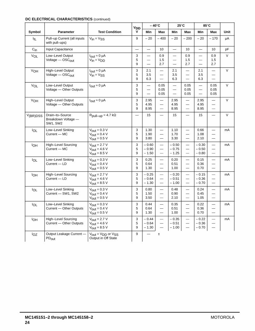
DC ELECTRICAL CHARACTERISTICS (continued)
Symbol Parameter Test ConditionVDD
V
– 40°C 25°C 85°C
UnitSymbol Parameter Test ConditionVDD
V Min Max Min Max Min Max Unit
IIL Pull–up Current (all inputswith pull–ups)
Vin = VSS 9 – 20 – 400 – 20 – 200 – 20 – 170 µA
Cin Input Capacitance — — 10 — 10 — 10 pF
VOL Low–Level OutputVoltage — OSCout
Iout ≈ 0 µAVin = VDD
359
———
0.91.52.7
———
0.91.52.7
———
0.91.52.7
V
VOH High–Level OutputVoltage — OSCout
Iout ≈ 0 µAVin = VSS
359
2.13.56.3
———
2.13.56.3
———
2.13.56.3
———
V
VOL Low–Level OutputVoltage — Other Outputs
Iout ≈ 0 µA 359
———
0.050.050.05
———
0.050.050.05
———
0.050.050.05
V
VOH High–Level OutputVoltage — Other Outputs
Iout ≈ 0 µA 359
2.954.958.95
———
2.954.958.95
———
2.954.958.95
———
V
V(BR)DSS Drain–to–SourceBreakdown Voltage —SW1, SW2
Rpull–up = 4.7 kΩ — 15 — 15 — 15 — V
IOL Low–Level SinkingCurrent — MC
Vout = 0.3 VVout = 0.4 VVout = 0.5 V
359
1.301.903.80
———
1.101.703.30
———
0.661.082.10
———
mA
IOH High–Level SourcingCurrent — MC
Vout = 2.7 VVout = 4.6 VVout = 8.5 V
359
– 0.60– 0.90– 1.50
———
– 0.50– 0.75– 1.25
———
– 0.30– 0.50– 0.80
———
mA
IOL Low–Level SinkingCurrent — LD
Vout = 0.3 VVout = 0.4 VVout = 0.5 V
359
0.250.641.30
———
0.200.511.00
———
0.150.360.70
———
mA
IOH High–Level SourcingCurrent — LD
Vout = 2.7 VVout = 4.6 VVout = 8.5 V
359
– 0.25– 0.64– 1.30
———
– 0.20– 0.51– 1.00
———
– 0.15– 0.36– 0.70
———
mA
IOL Low–Level SinkingCurrent — SW1, SW2
Vout = 0.3 VVout = 0.4 VVout = 0.5 V
359
0.801.503.50
———
0.480.902.10
———
0.240.451.05
———
mA
IOL Low–Level SinkingCurrent — Other Outputs
Vout = 0.3 VVout = 0.4 VVout = 0.5 V
359
0.440.641.30
———
0.350.511.00
———
0.220.360.70
———
mA
IOH High–Level SourcingCurrent — Other Outputs
Vout = 2.7 VVout = 4.6 VVout = 8.5 V
359
– 0.44– 0.64– 1.30
———
– 0.35– 0.51– 1.00
———
– 0.22– 0.36– 0.70
———
mA
IOZ Output Leakage Current —PDout
Vout = VDD or VSSOutput in Off State
9 — ± 0.3 — ± 0.1 — ± 1.0 µA
IOZ Output Leakage Current —SW1, SW2
Vout = VDD or VSSOutput in Off State
9 — ± 0.3 — ± 0.1 — ± 3.0 µA
Cout Output Capacitance —PDout
PDout — Three–State — — 10 — 10 — 10 pF

MC145151–2 through MC145158–2MOTOROLA25
AC ELECTRICAL CHARACTERISTICS (CL = 50 pF, Input tr = tf = 10 ns)
Symbol ParameterVDD
VGuaranteed Limit
25°CGuaranteed Limit
– 40 to 85°C Unit
tPLH, tPHL Maximum Propagation Delay, fin to MC(Figures 1 and 4)
359
1106035
1207040
ns
tPHL Maximum Propagation Delay, ENB to SW1, SW2(Figures 1 and 5)
359
1608050
1809560
ns
tw Output Pulse Width, φR, φV, and LD with fR in Phase with fV(Figures 2 and 4)
359
25 to 20020 to 10010 to 70
25 to 26020 to 12510 to 80
ns
tTLH Maximum Output Transition Time, MC(Figures 3 and 4)
359
1156040
1157560
ns
tTHL Maximum Output Transition Time, MC(Figures 3 and 4)
359
603430
704538
ns
tTLH, tTHL Maximum Output Transition Time, LD(Figures 3 and 4)
359
1809070
20012090
ns
tTLH, tTHL Maximum Output Transition Time, Other Outputs(Figures 3 and 4)
359
1608060
17510065
ns
SWITCHING WAVEFORMS
TEST POINT
DEVICEUNDERTEST
CL*
* Includes all probe and fixture capacitance.
TEST POINT
DEVICEUNDERTEST
CL*
* Includes all probe and fixture capacitance.
VDD
15 kΩ
tTLH
90%
10%
tTHLANY
OUTPUT
Figure 1. Figure 2.
50%OUTPUT
50%INPUT
tPLH
— VSS
VDD
tPHL 50%φR, φV, LD*
* fR in phase with fV.
tw
OUTPUTOUTPUT
Figure 3.
Figure 4. Test Circuit Figure 5. Test Circuit

MC145151–2 through MC145158–2 MOTOROLA26
TIMING REQUIREMENTS (Input tr = tf = 10 ns unless otherwise indicated)
Symbol ParameterVDD
VGuaranteed Limit
25°CGuaranteed Limit
– 40 to 85°C Unit
fclk Serial Data Clock Frequency, Assuming 25% Duty CycleNOTE: Refer to CLK tw(H) below
(Figure 6)
359
dc to 5.0dc to 7.1dc to 10
dc to 3.5dc to 7.1dc to 10
MHz
tsu Minimum Setup Time, Data to CLK(Figure 7)
359
302018
302018
ns
th Minimum Hold Time, CLK to Data(Figure 7)
359
402015
402015
ns
tsu Minimum Setup Time, CLK to ENB(Figure 7)
359
703225
703225
ns
trec Minimum Recovery Time, ENB to CLK(Figure 7)
359
51020
51020
ns
tw(H) Minimum Pulse Width, CLK and ENB(Figure 6)
359
503525
703525
ns
tr, tf Maximum Input Rise and Fall Times — Any Input(Figure 8)
359
542
542
µs
SWITCHING WAVEFORMS
Figure 6.
Figure 7. VSS
— VDD
50%
50%
LASTCLK
PREVIOUSDATA
LATCHED
FIRSTCLK
ENB
CLK
DATA 50%— VDD
VSS
— VDD
VSS
— VDD
VSS
tsu
tsu trec
th50%
CLK,ENB
tw(H)— VDD
VSS4 fclk
1 *
*Assumes 25% Duty Cycle.
tt
90%
10%
tfANY
OUTPUT
Figure 8.

MC145151–2 through MC145158–2MOTOROLA27
FREQUENCY CHARACTERISTICS (Voltages References to VSS, CL = 50 pF, Input tr = tf =10 ns unless otherwise indicated)
Symbol Parameter Test ConditionVDD
V
– 40°C 25°C 85°C
UnitSymbol Parameter Test ConditionVDD
V Min Max Min Max Min Max Unit
fi Input Frequency(fin, OSCin)
R ≥ 8, A ≥ 0, N ≥ 8Vin = 500 mV p–pac coupled sine wave
359
———
61515
———
61515
———
61515
MHz
R ≥ 8, A ≥ 0, N ≥ 8Vin = 1 V p–p ac coupledsine wave
359
———
122225
———
122022
———
72022
MHz
R ≥ 8, A ≥ 0, N ≥ 8Vin = VDD to VSSdc coupled square wave
359
———
132525
———
122225
———
82225
MHz
NOTE: Usually, the PLL’s propagation delay from fin to MC plus the setup time of the prescaler determines the upper frequency limit of the system.The upper frequency limit is found with the following formula: f = P / (tP + tset) where f is the upper frequency in Hz, P is the lower of the dualmodulus prescaler ratios, tP is the fin to MC propagation delay in seconds, and tset is the prescaler setup time in seconds.For example, with a 5 V supply, the fin to MC delay is 70 ns. If the MC12028A prescaler is used, the setup time is 16 ns. Thus, if the 64/65ratio is utilized, the upper frequency limit is f = P / (tP + tset) = 64/(70 + 16) = 744 MHz.
VH = High Voltage Level.VL = Low Voltage Level.* At this point, when both fR and fV are in phase, the output is forced to near mid–supply.NOTE: The PDout generates error pulses during out–of–lock conditions. When locked in phase and frequency the output is high
and the voltage at this pin is determined by the low–pass filter capacitor.
fRREFERENCE
OSC ÷ R
fVFEEDBACK
(fin ÷ N)
PDout
φR
φV
LD
*
VH
VLVH
VLVH
HIGH IMPEDANCE
VH
VLVH
VLVH
VL
VL
Figure 9. Phase Detector/Lock Detector Output Waveforms

MC145151–2 through MC145158–2 MOTOROLA28
DESIGN CONSIDERATIONS
PHASE–LOCKED LOOP — LOW–PASS FILTER DESIGN
C)
_
+ A
C
R2
C
VCO
C
VCO
R2
B)
A)
C
VCOPDout
PDout
φR —
φV —
PDout —
φRφV
R1
R1
R1
R1
R2
NOTE: Sometimes R1 is split into two series resistors, each R1 ÷ 2. A capacitor CC is then placed from the midpoint to ground to furtherfilter φV and φR. The value of CC should be such that the corner frequency of this network does not significantly affect ωn.The φR and φV outputs swing rail–to–rail. Therefore, the user should be careful not to exceed the common mode input range of theop amp used in the combiner/loop filter.
DEFINITIONS:N = Total Division Ratio in feedback loopKφ (Phase Detector Gain) = VDD/4π for PDoutKφ (Phase Detector Gain) = VDD/2π for φV and φR
KVCO (VCO Gain) =2π∆fVCO∆VVCO
for a typical design wn (Natural Frequency) ≈ 2πfr10
(at phase detector input).
Damping Factor: ζ ≅ 1
RECOMMENDED READING:Gardner, Floyd M., Phaselock Techniques (second edition). New York, Wiley–Interscience, 1979.Manassewitsch, Vadim, Frequency Synthesizers: Theory and Design (second edition). New York, Wiley–Interscience, 1980.Blanchard, Alain, Phase–Locked Loops: Application to Coherent Receiver Design. New York, Wiley–Interscience, 1976.Egan, William F., Frequency Synthesis by Phase Lock. New York, Wiley–Interscience, 1981.Rohde, Ulrich L., Digital PLL Frequency Synthesizers Theory and Design. Englewood Cliffs, NJ, Prentice–Hall, 1983.Berlin, Howard M., Design of Phase–Locked Loop Circuits, with Experiments. Indianapolis, Howard W. Sams and Co., 1978.Kinley, Harold, The PLL Synthesizer Cookbook. Blue Ridge Summit, PA, Tab Books, 1980.AN535, Phase–Locked Loop Design Fundamentals, Motorola Semiconductor Products, Inc., 1970.AR254, Phase–Locked Loop Design Articles, Motorola Semiconductor Products, Inc., Reprinted with permission from Electronic Design,
1987.
φR —
φV —
F(s) =
ASSUMING GAIN A IS VERY LARGE, THEN:
F(s) =
ζ =
ωn = NR1C
R1sC + 1
ωn =
ζ =ωnR2C
2
R2sC + 1
R1sC
1
Nωn2KφKVCO
F(s) =
ζ =
ωn =
(R1 + R2)sC + 1
R2sC + 1
NC(R1 + R2)
R2C +N
KφKVCO
KφKVCONCR1
0.5 ωn
KφKVCO
KφKVCO

MC145151–2 through MC145158–2MOTOROLA29
CRYSTAL OSCILLATOR CONSIDERATIONS
The following options may be considered to provide a ref-erence frequency to Motorola’s CMOS frequency synthe-sizers.
Use of a Hybrid Crystal Oscillator
Commercially available temperature–compensated crystaloscillators (TCXOs) or crystal–controlled data clock oscilla-tors provide very stable reference frequencies. An oscillatorcapable of sinking and sourcing 50 µA at CMOS logic levelsmay be direct or dc coupled to OSCin. In general, the highestfrequency capability is obtained utilizing a direct–coupledsquare wave having a rail–to–rail (VDD to VSS) voltageswing. If the oscillator does not have CMOS logic levels onthe outputs, capacitive or ac coupling to OSCin may be used.OSCout, an unbuffered output, should be left floating.
For additional information about TCXOs and data clockoscillators, please consult the latest version of the eem Elec-tronic Engineers Master Catalog, the Gold Book, or similarpublications.
Design an Off–Chip Reference
The user may design an off–chip crystal oscillator usingICs specifically developed for crystal oscillator applications,such as the MC12061 MECL device. The reference signalfrom the MECL device is ac coupled to OSCin. For large am-plitude signals (standard CMOS logic levels), dc coupling isused. OSCout, an unbuffered output, should be left floating.In general, the highest frequency capability is obtained with adirect–coupled square wave having rail–to–rail voltageswing.
Use of the On–Chip Oscillator Circuitry
The on–chip amplifier (a digital inverter) along with an ap-propriate crystal may be used to provide a reference sourcefrequency. A fundamental mode crystal, parallel resonant atthe desired operating frequency, should be connected asshown in Figure 10.
Figure 10. Pierce Crystal Oscillator Circuit
R1*
C2C1
FREQUENCYSYNTHESIZER
OSCoutOSCin
* May be deleted in certain cases. See text.
Rf
For VDD = 5.0 V, the crystal should be specified for a load-ing capacitance, CL, which does not exceed 32 pF for fre-quencies to approximately 8.0 MHz, 20 pF for frequencies inthe area of 8.0 to 15 MHz, and 10 pF for higher frequencies.These are guidelines that provide a reasonable compromisebetween IC capacitance, drive capability, swamping varia-tions in stray and IC input/output capacitance, and realistic
CL values. The shunt load capacitance, CL, presentedacross the crystal can be estimated to be:
CL =CinCout
Cin + Cout+ Ca + Co + C1 • C2
C1 + C2
whereCin = 5 pF (see Figure 11)
Cout = 6 pF (see Figure 11)Ca = 1 pF (see Figure 11)CO = the crystal’s holder capacitance
(see Figure 12)C1 and C2 = external capacitors (see Figure 10)
Figure 11. Parasitic Capacitances of the Amplifier
Cin Cout
Ca
Figure 12. Equivalent Crystal Networks
NOTE: Values are supplied by crystal manufacturer(parallel resonant crystal).
21
2121
RS LS CS
Re Xe
CO
The oscillator can be “trimmed” on–frequency by making aportion or all of C1 variable. The crystal and associated com-ponents must be located as close as possible to the OSCinand OSCout pins to minimize distortion, stray capacitance,stray inductance, and startup stabilization time. In somecases, stray capacitance should be added to the value for Cinand Cout.
Power is dissipated in the effective series resistance of thecrystal, Re, in Figure 12. The drive level specified by the crys-tal manufacturer is the maximum stress that a crystal canwithstand without damage or excessive shift in frequency. R1in Figure 10 limits the drive level. The use of R1 may not benecessary in some cases (i.e., R1 = 0 Ω).
To verify that the maximum dc supply voltage does notoverdrive the crystal, monitor the output frequency as a func-tion of voltage at OSCout. (Care should be taken to minimizeloading.) The frequency should increase very slightly as thedc supply voltage is increased. An overdriven crystal will de-crease in frequency or become unstable with an increase insupply voltage. The operating supply voltage must be re-duced or R1 must be increased in value if the overdrivencondition exists. The user should note that the oscillatorstart–up time is proportional to the value of R1.
Through the process of supplying crystals for use withCMOS inverters, many crystal manufacturers have devel-oped expertise in CMOS oscillator design with crystals. Dis-cussions with such manufacturers can prove very helpful(see Table 1).

MC145151–2 through MC145158–2 MOTOROLA30
Table 1. Partial List of Crystal Manufacturers
Name Address Phone
United States Crystal Corp.Crystek CrystalStatek Corp.
3605 McCart Ave., Ft. Worth, TX 761102351 Crystal Dr., Ft. Myers, FL 33907512 N. Main St., Orange, CA 92668
(817) 921–3013(813) 936–2109(714) 639–7810
NOTE: Motorola cannot recommend one supplier over another and in no way suggests that this is a completelisting of crystal manufacturers.
RECOMMENDED READING
Technical Note TN–24, Statek Corp.Technical Note TN–7, Statek Corp.E. Hafner, “The Piezoelectric Crystal Unit – Definitions and
Method of Measurement”, Proc. IEEE, Vol. 57, No. 2 Feb.,1969.
D. Kemper, L. Rosine, “Quartz Crystals for FrequencyControl”, Electro–Technology, June, 1969.
P. J. Ottowitz, “A Guide to Crystal Selection”, ElectronicDesign, May, 1966.
DUAL–MODULUS PRESCALING
OVERVIEW
The technique of dual–modulus prescaling is well estab-lished as a method of achieving high performance frequencysynthesizer operation at high frequencies. Basically, theapproach allows relatively low–frequency programmablecounters to be used as high–frequency programmablecounters with speed capability of several hundred MHz. Thisis possible without the sacrifice in system resolution and per-formance that results if a fixed (single–modulus) divider isused for the prescaler.
In dual–modulus prescaling, the lower speed countersmust be uniquely configured. Special control logic is neces-sary to select the divide value P or P + 1 in the prescaler forthe required amount of time (see modulus control definition).Motorola’s dual–modulus frequency synthesizers containthis feature and can be used with a variety of dual–modulusprescalers to allow speed, complexity and cost to be tailoredto the system requirements. Prescalers having P, P + 1 di-vide values in the range of ÷ 3/÷ 4 to ÷ 128/÷ 129 can be con-trolled by most Motorola frequency synthesizers.
Several dual–modulus prescaler approaches suitable foruse with the MC145152–2, MC145156–2, or MC145158–2are:
MC12009MC12011MC12013MC12015MC12016MC12017MC12018MC12022AMC12032A
÷ 5/÷ 6÷ 8/÷ 9
÷ 10/÷ 11÷ 32/÷ 33÷ 40/÷ 41÷ 64/÷ 65
÷ 128/÷ 129÷ 64/65 or ÷ 128/129÷ 64/65 or ÷ 128/129
440 MHz500 MHz500 MHz225 MHz225 MHz225 MHz520 MHz1.1 GHz2.0 GHz
DESIGN GUIDELINES
The system total divide value, Ntotal (NT) will be dictated bythe application:
NT =frequency into the prescaler
frequency into the phase detector= N P + A
N is the number programmed into the ÷ N counter, A is thenumber programmed into the ÷ A counter, P and P + 1 arethe two selectable divide ratios available in the dual–modu-lus prescalers. To have a range of NT values in sequence,the ÷ A counter is programmed from zero through P – 1 for aparticular value N in the ÷ N counter. N is then incremented toN + 1 and the ÷ A is sequenced from 0 through P – 1 again.
There are minimum and maximum values that can beachieved for NT. These values are a function of P and thesize of the ÷ N and ÷ A counters.
The constraint N ≥ A always applies. If Amax = P – 1, thenNmin ≥ P – 1. Then NTmin = (P – 1) P + A or (P – 1) P since Ais free to assume the value of 0.
NTmax = Nmax P + Amax
To maximize system frequency capability, the dual–modu-lus prescaler output must go from low to high after eachgroup of P or P + 1 input cycles. The prescaler should divideby P when its modulus control line is high and by P + 1 whenits MC is low.
For the maximum frequency into the prescaler (fVCOmax),the value used for P must be large enough such that:
1. fVCOmax divided by P may not exceed the frequencycapability of fin (input to the ÷ N and ÷ A counters).
2. The period of fVCO divided by P must be greater thanthe sum of the times:
a. Propagation delay through the dual–modulus pre-scaler.
b. Prescaler setup or release time relative to its MCsignal.
c. Propagation time from fin to the MC output for thefrequency synthesizer device.
A sometimes useful simplification in the programmingcode can be achieved by choosing the values for P of 8, 16,32, or 64. For these cases, the desired value of NT resultswhen NT in binary is used as the program code to the ÷ N and÷ A counters treated in the following manner:
1. Assume the ÷ A counter contains “a” bits where 2a ≥ P.
2. Always program all higher order ÷ A counter bits above“a” to 0.
3. Assume the ÷ N counter and the ÷ A counter (with all thehigher order bits above “a” ignored) combined into asingle binary counter of n + a bits in length (n = numberof divider stages in the ÷ N counter). The MSB of this “hy-pothetical” counter is to correspond to the MSB of ÷ N andthe LSB is to correspond to the LSB of ÷ A. The systemdivide value, NT, now results when the value of NT inbinary is used to program the “new” n + a bit counter.
By using the two devices, several dual–modulus valuesare achievable (shown in Figure 13).
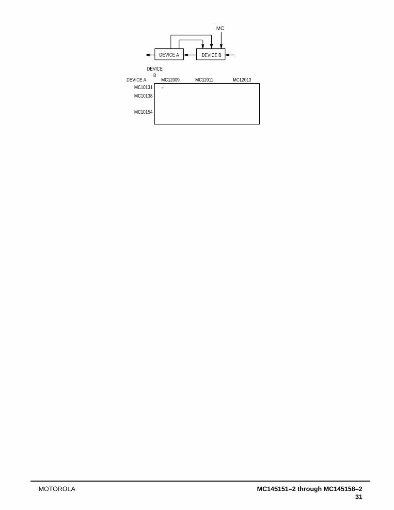
MC145151–2 through MC145158–2MOTOROLA31
MC
DEVICE BDEVICE A
DEVICEB
MC12009 MC12011 MC12013DEVICE AMC10131
MC10138
MC10154
÷ 20/÷ 21
÷ 50/÷ 51
÷ 40/÷ 41OR
÷ 80/÷ 81
÷ 64/÷ 65OR
÷ 128/÷ 129
÷ 32/÷ 33
÷ 80/÷ 81
÷ 40/÷ 41
÷ 100/÷ 101
÷ 80/÷ 81
NOTE: MC12009, MC12011, and MC12013 are pin equivalent.MC12015, MC12016, and MC12017 are pin equivalent.
Figure 13. Dual–Modulus Values
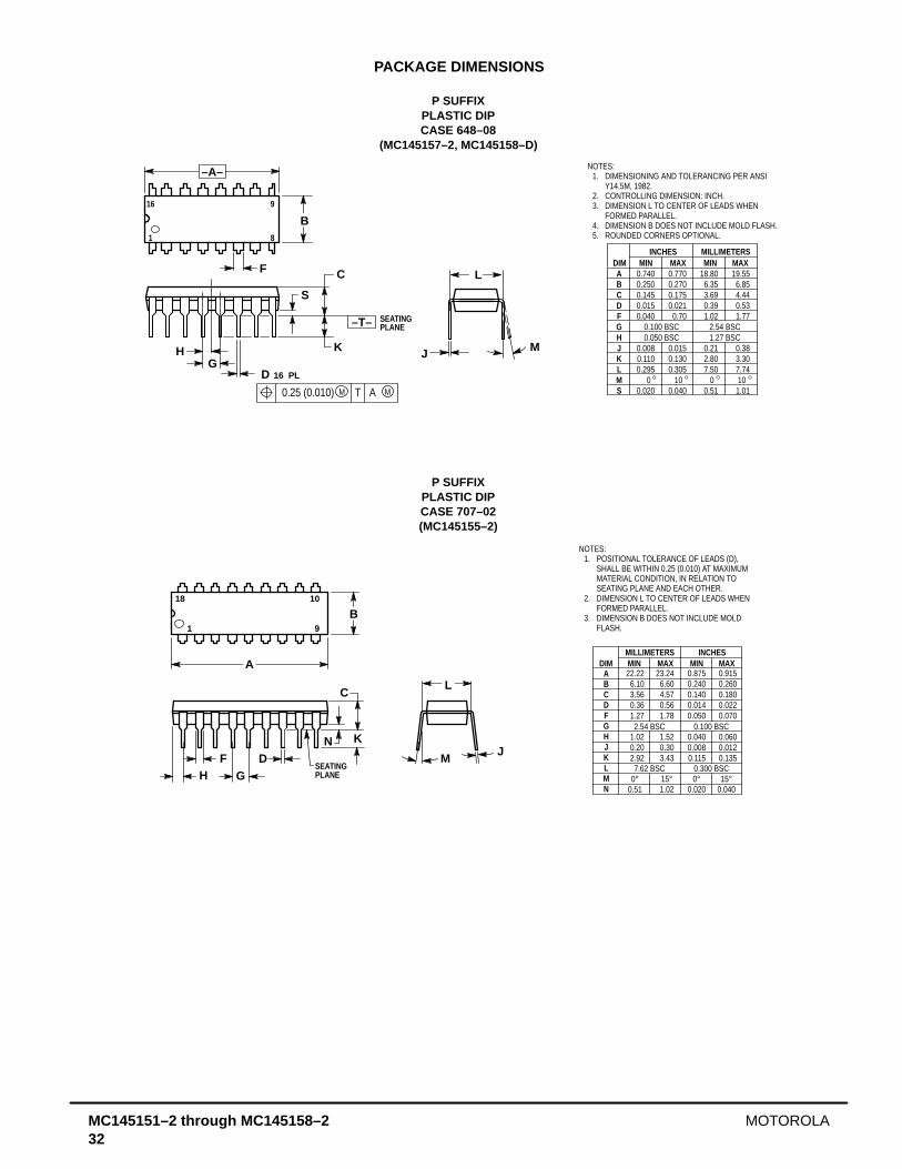
MC145151–2 through MC145158–2 MOTOROLA32
PACKAGE DIMENSIONS
P SUFFIXPLASTIC DIPCASE 648–08
(MC145157–2, MC145158–D)
NOTES:1. DIMENSIONING AND TOLERANCING PER ANSI
Y14.5M, 1982.2. CONTROLLING DIMENSION: INCH.3. DIMENSION L TO CENTER OF LEADS WHEN
FORMED PARALLEL.4. DIMENSION B DOES NOT INCLUDE MOLD FLASH.5. ROUNDED CORNERS OPTIONAL.
–A–
B
F C
S
HG
D
J
L
M
16 PL
SEATING
1 8
916
K
PLANE–T–
MAM0.25 (0.010) T
DIM MIN MAX MIN MAXMILLIMETERSINCHES
A 0.740 0.770 18.80 19.55B 0.250 0.270 6.35 6.85C 0.145 0.175 3.69 4.44D 0.015 0.021 0.39 0.53F 0.040 0.70 1.02 1.77G 0.100 BSC 2.54 BSCH 0.050 BSC 1.27 BSCJ 0.008 0.015 0.21 0.38K 0.110 0.130 2.80 3.30L 0.295 0.305 7.50 7.74M 0 10 0 10 S 0.020 0.040 0.51 1.01
P SUFFIXPLASTIC DIPCASE 707–02(MC145155–2)
MIN MINMAX MAXMILLIMETERS INCHES
DIM22.226.103.560.361.27
1.020.202.92
23.246.604.570.561.78
1.520.303.43
0°0.51
0.8750.2400.1400.0140.050
0.0400.0080.115
0.9150.2600.1800.0220.070
0.0600.0120.135
15°1.02
2.54 BSC
7.62 BSC
0.100 BSC
0.300 BSC0°
0.02015°
0.040
ABCDFGHJKLMN
NOTES:1. POSITIONAL TOLERANCE OF LEADS (D),
SHALL BE WITHIN 0.25 (0.010) AT MAXIMUMMATERIAL CONDITION, IN RELATION TOSEATING PLANE AND EACH OTHER.
2. DIMENSION L TO CENTER OF LEADS WHENFORMED PARALLEL.
3. DIMENSION B DOES NOT INCLUDE MOLDFLASH.1 9
1018
B
A
HF
GD
SEATINGPLANE
N K
MJ
LC

MC145151–2 through MC145158–2MOTOROLA33
P SUFFIXPLASTIC DIPCASE 710–02
(MC145151–2, MC145152–2)
0.100 BSC
0.600 BSC
2.54 BSC
15.24 BSC
MIN MINMAX MAXMILLIMETERS INCHES
DIM36.4513.723.940.361.02
1.650.202.92
0° 0.51
37.2114.225.080.561.52
2.160.383.43
15° 1.02
1.4350.5400.1550.0140.040
0.0650.0080.115
0° 0.020
1.4650.5600.2000.0220.060
0.0850.0150.135
15° 0.040
ABCDFGHJKLMN
NOTES:1. POSITIONAL TOLERANCE OF LEADS (D),
SHALL BE WITHIN 0.25mm (0.010) ATMAXIMUM MATERIAL CONDITION, INRELATION TO SEATING PLANE ANDEACH OTHER.
2. DIMENSION L TO CENTER OF LEADSWHEN FORMED PARALLEL.
3. DIMENSION B DOES NOT INCLUDEMOLD FLASH.
1 14
1528
B
A C
N
K MJ
DSEATINGPLANE
FH G
L
P SUFFIXPLASTIC DIPCASE 738–03(MC145156–2)
1.0700.2600.1800.022
0.070
0.0150.140
15° 0.040
1.0100.2400.1500.015
0.050
0.0080.110
0° 0.020
25.666.103.810.39
1.27
0.212.80
0° 0.51
27.176.604.570.55
1.77
0.383.55
15°1.01
0.050 BSC
0.100 BSC
0.300 BSC
1.27 BSC
2.54 BSC
7.62 BSC
MIN MINMAX MAXINCHES MILLIMETERS
DIMABCDEFGJKLMN
NOTES:1. DIMENSIONING AND TOLERANCING PER ANSI
Y14.5M, 1982.2. CONTROLLING DIMENSION: INCH.3. DIMENSION L TO CENTER OF LEAD WHEN
FORMED PARALLEL.4. DIMENSION B DOES NOT INCLUDE MOLD
FLASH.
-A-
C
K
NE
G F
D 20 PL
J 20 PL
L
M
-T-SEATINGPLANE
1 10
1120
0.25 (0.010) T AM M
0.25 (0.010) T BM M
B

MC145151–2 through MC145158–2 MOTOROLA34
DW SUFFIXSOG PACKAGECASE 751D–04
(MC145155–2, MC145156–2)
NOTES:1. DIMENSIONING AND TOLERANCING PER
ANSI Y14.5M, 1982.2. CONTROLLING DIMENSION: MILLIMETER.3. DIMENSIONS A AND B DO NOT INCLUDE
MOLD PROTRUSION.4. MAXIMUM MOLD PROTRUSION 0.150
(0.006) PER SIDE.5. DIMENSION D DOES NOT INCLUDE
DAMBAR PROTRUSION. ALLOWABLEDAMBAR PROTRUSION SHALL BE 0.13(0.005) TOTAL IN EXCESS OF D DIMENSIONAT MAXIMUM MATERIAL CONDITION.
–A–
–B–
20
1
11
10
SAM0.010 (0.25) B ST
D20X
MBM0.010 (0.25)P10X
J
F
G18X K
C
–T– SEATINGPLANE
M
R X 45
DIM MIN MAX MIN MAXINCHESMILLIMETERS
A 12.65 12.95 0.499 0.510B 7.40 7.60 0.292 0.299C 2.35 2.65 0.093 0.104D 0.35 0.49 0.014 0.019F 0.50 0.90 0.020 0.035G 1.27 BSC 0.050 BSCJ 0.25 0.32 0.010 0.012K 0.10 0.25 0.004 0.009M 0 7 0 7 P 10.05 10.55 0.395 0.415R 0.25 0.75 0.010 0.029
DW SUFFIXSOG PACKAGECASE 751F–04
(MC145151–2, MC145152–2)
MIN MINMAX MAXMILLIMETERS INCHES
DIMABCDFGJKMPR
17.807.402.350.350.41
0.230.13
0° 10.050.25
18.057.602.650.490.90
0.320.29
8° 10.550.75
0.7010.2920.0930.0140.016
0.0090.005
0° 0.3950.010
0.7110.2990.1040.0190.035
0.0130.011
8° 0.4150.029
1.27 BSC 0.050 BSC
NOTES:1. DIMENSIONING AND TOLERANCING PER
ANSI Y14.5M, 1982.2. CONTROLLING DIMENSION: MILLIMETER.3. DIMENSION A AND B DO NOT INCLUDE MOLD
PROTRUSION.4. MAXIMUM MOLD PROTRUSION 0.15
(0.006) PER SIDE.5. DIMENSION D DOES NOT INCLUDE
DAMBAR PROTRUSION. ALLOWABLEDAMBAR PROTRUSION SHALL BE 0.13(0.005) TOTAL IN EXCESS OF DDIMENSION AT MAXIMUM MATERIALCONDITION.
-A-
-B-
1 14
1528
-T- C
SEATINGPLANE
0.010 (0.25) BM M
M
J
-T-
K
26X G
28X D
14X P
R X 45°
F
0.010 (0.25) T A BM S S

MC145151–2 through MC145158–2MOTOROLA35
DW SUFFIXSOG PACKAGECASE 751G–02
(MC145157–2, MC145158–2)
DIM MIN MAX MIN MAXINCHESMILLIMETERS
A 10.15 10.45 0.400 0.411B 7.40 7.60 0.292 0.299C 2.35 2.65 0.093 0.104D 0.35 0.49 0.014 0.019F 0.50 0.90 0.020 0.035G 1.27 BSC 0.050 BSCJ 0.25 0.32 0.010 0.012K 0.10 0.25 0.004 0.009M 0 7 0 7 P 10.05 10.55 0.395 0.415R 0.25 0.75 0.010 0.029
MBM0.010 (0.25)
NOTES:1. DIMENSIONING AND TOLERANCING PER ANSI
Y14.5M, 1982.2. CONTROLLING DIMENSION: MILLIMETER.3. DIMENSIONS A AND B DO NOT INCLUDE MOLD
PROTRUSION.4. MAXIMUM MOLD PROTRUSION 0.15 (0.006) PER
SIDE.5. DIMENSION D DOES NOT INCLUDE DAMBAR
PROTRUSION. ALLOWABLE DAMBARPROTRUSION SHALL BE 0.13 (0.005) TOTAL INEXCESS OF D DIMENSION AT MAXIMUMMATERIAL CONDITION.
–A–
–B– P8X
G14X
D16X
SEATINGPLANE
–T–
SAM0.010 (0.25) B ST
16 9
81
F
J
R X 45
M
C
K

MC145151–2 through MC145158–2 MOTOROLA36
Motorola reserves the right to make changes without further notice to any products herein. Motorola makes no warranty, representation or guarantee regardingthe suitability of its products for any particular purpose, nor does Motorola assume any liability arising out of the application or use of any product or circuit,and specifically disclaims any and all liability, including without limitation consequential or incidental damages. “Typical” parameters can and do vary in differentapplications. All operating parameters, including “Typicals” must be validated for each customer application by customer’s technical experts. Motorola doesnot convey any license under its patent rights nor the rights of others. Motorola products are not designed, intended, or authorized for use as components insystems intended for surgical implant into the body, or other applications intended to support or sustain life, or for any other application in which the failure ofthe Motorola product could create a situation where personal injury or death may occur. Should Buyer purchase or use Motorola products for any suchunintended or unauthorized application, Buyer shall indemnify and hold Motorola and its officers, employees, subsidiaries, affiliates, and distributors harmlessagainst all claims, costs, damages, and expenses, and reasonable attorney fees arising out of, directly or indirectly, any claim of personal injury or deathassociated with such unintended or unauthorized use, even if such claim alleges that Motorola was negligent regarding the design or manufacture of the part.Motorola and are registered trademarks of Motorola, Inc. Motorola, Inc. is an Equal Opportunity/Affirmative Action Employer.
How to reach us:USA/EUROPE: Motorola Literature Distribution; JAPAN : Nippon Motorola Ltd.; Tatsumi–SPD–JLDC, Toshikatsu Otsuki,P.O. Box 20912; Phoenix, Arizona 85036. 1–800–441–2447 6F Seibu–Butsuryu–Center, 3–14–2 Tatsumi Koto–Ku, Tokyo 135, Japan. 03–3521–8315
MFAX: [email protected] – TOUCHTONE (602) 244–6609 HONG KONG: Motorola Semiconductors H.K. Ltd.; 8B Tai Ping Industrial Park, INTERNET: http://Design–NET.com 51 Ting Kok Road, Tai Po, N.T., Hong Kong. 852–26629298
MC145151–2/D
◊