MAX3394E/MAX3395E/ ±15kV ESD-Protected Hih … MAX3394E/MAX3395E/MAX3396E feature a tri-state...
21
General Description The MAX3394E/MAX3395E/MAX3396E bidirectional level translators provide level shifting required for data transfer in a multivoltage system. Internal slew-rate enhancement circuitry features 10mA current-sink and 15mA current- source drivers to isolate capacitive loads from lower current drivers. In open-drain systems, slew-rate enhancement enables fast data rates with larger pullup resistors and increased bus load capacitance. Externally applied volt- ages, V CC and V L , set the logic-high levels for the device. A logic-low signal on one I/O side of the device appears as a logic-low signal on the opposite I/O side, and vice-versa. Each I/O line is pulled up to V CC or V L by an internal pullup resistor, allowing the devices to be driven by either push- pull or open-drain drivers. The MAX3394E/MAX3395E/MAX3396E feature a tri- state output mode, thermal-shutdown protection, and ±15kV Human Body Model (HBM) ESD protection on the V CC side for greater protection in applications that route signals externally. The MAX3394E/MAX3395E/MAX3396E accept V CC volt- ages from +1.65V to +5.5V, and V L voltages from +1.2V to V CC , making them ideal for data transfer between low voltage ASIC/PLDs and higher voltage systems. The MAX3394E/MAX3395E/MAX3396E operate at a guaran- teed data rate of 6Mbps with push-pull drivers and 1Mbps with open-drain drivers. The MAX3394E is a dual-level translator available in 9-bump UCSP™ and 8-pin 3mm x 3mm TDFN packages. The MAX3395E is a quad-level translator available in 12-bump UCSP, and 12-pin 4mm x 4mm TQFN packag- es. The MAX3396E is an octal-level translator available in 20-bump UCSP and 20-pin 5mm x 5mm TQFN packages. The MAX3394E/MAX3395E/MAX3396E operate over the extended -40°C to +85°C temperature range. Applications ● Multivoltage Bidirectional Level Translation ● SPI™, MICROWIRE™, and I 2 C Level Translation ● Open-Drain Rise-Time Speed-Up ● High-Speed Bus Fan-Out Expansion ● Cell Phones ● Telecom, Networking, Servers, RAID/SAN Features ● ±15kV ESD Protection on I/O V CC_ Lines ● Bidirectional Level Translation Without Direction Pin ● I/O V L_ and I/O V CC_ 10mA Sink-/15mA Source- Current Capability ● Slew-Rate Enhancement Circuitry Supports ● Larger Capacitive Loads or Larger External Pullup Resistors ● 6Mbps Push-Pull/1Mbps Open-Drain Guaranteed Data Rate ● Wide Supply-Voltage Range: Operation Down to +1.2V on V L and +1.65V on V CC ● Low Supply Current in Tri-State Output Mode (3μA typ) ● Low Quiescent Current ● Thermal-Shutdown Protection ● UCSP, TDFN, and TQFN Packages 19-3884; Rev 3; 7/17 MICROWIRE is a trademark of National Semiconductor Corp. SPI is a trademark of Motorola, Inc. UCSP is a trademark of Maxim Integrated Products, Inc. Selector Guide appears at end of data sheet. Note: All devices specified over the -40°C to +85°C operating range. +Denotes lead(Pb)-free/RoHS-compliant package. *Future product—contact factory for availability. **EP = Exposed paddle. PART PIN-PACKAGE PKG CODE MAX3394EETA+T 8 TDFN-EP** T833-1 MAX3394EEBL+T 9 UCSP B9-5 MAX3395EETC+ 12 TQFN-EP** T1244-4 MAX3395EEBC+T 12 UCSP B12-1 MAX3396EEBP+T* 20 UCSP B20-1 MAX3396EETP+* 20 TQFN-EP** T2055-4 1 2 3 4 8 7 6 5 V L I/O V L 1 I/O V L 2 GND *CONNECT EXPOSED PAD TO GROUND *EP I/O V CC 2 I/O V CC 1 EN V CC MAX3394E TDFN TOP VIEW (LEADS ON BOTTOM) + Pin Configurations continued at end of data sheet. MAX3394E/MAX3395E/ MAX3396E ±15kV ESD-Protected, High-Drive Current, Dual-/Quad-/Octal-Level Translators with Speed-Up Circuitry Pin Configurations Ordering Information
Transcript of MAX3394E/MAX3395E/ ±15kV ESD-Protected Hih … MAX3394E/MAX3395E/MAX3396E feature a tri-state...

General DescriptionThe MAX3394E/MAX3395E/MAX3396E bidirectional level translators provide level shifting required for data transfer in a multivoltage system. Internal slew-rate enhancement circuitry features 10mA current-sink and 15mA current-source drivers to isolate capacitive loads from lower current drivers. In open-drain systems, slew-rate enhancement enables fast data rates with larger pullup resistors and increased bus load capacitance. Externally applied volt-ages, VCC and VL, set the logic-high levels for the device. A logic-low signal on one I/O side of the device appears as a logic-low signal on the opposite I/O side, and vice-versa. Each I/O line is pulled up to VCC or VL by an internal pullup resistor, allowing the devices to be driven by either push-pull or open-drain drivers.The MAX3394E/MAX3395E/MAX3396E feature a tri-state output mode, thermal-shutdown protection, and ±15kV Human Body Model (HBM) ESD protection on the VCC side for greater protection in applications that route signals externally.The MAX3394E/MAX3395E/MAX3396E accept VCC volt-ages from +1.65V to +5.5V, and VL voltages from +1.2V to VCC, making them ideal for data transfer between low voltage ASIC/PLDs and higher voltage systems. The MAX3394E/MAX3395E/MAX3396E operate at a guaran-teed data rate of 6Mbps with push-pull drivers and 1Mbps with open-drain drivers.The MAX3394E is a dual-level translator available in 9-bump UCSP™ and 8-pin 3mm x 3mm TDFN packages. The MAX3395E is a quad-level translator available in 12-bump UCSP, and 12-pin 4mm x 4mm TQFN packag-es. The MAX3396E is an octal-level translator available in 20-bump UCSP and 20-pin 5mm x 5mm TQFN packages. The MAX3394E/MAX3395E/MAX3396E operate over the extended -40°C to +85°C temperature range.
Applications Multivoltage Bidirectional Level Translation SPI™, MICROWIRE™, and I2C Level Translation Open-Drain Rise-Time Speed-Up High-Speed Bus Fan-Out Expansion Cell Phones Telecom, Networking, Servers, RAID/SAN
Features ±15kV ESD Protection on I/O VCC_ Lines Bidirectional Level Translation Without Direction Pin I/O VL_ and I/O VCC_ 10mA Sink-/15mA Source-
Current Capability Slew-Rate Enhancement Circuitry Supports Larger Capacitive Loads or Larger External Pullup
Resistors 6Mbps Push-Pull/1Mbps Open-Drain Guaranteed
Data Rate Wide Supply-Voltage Range: Operation Down to
+1.2V on VL and +1.65V on VCC Low Supply Current in Tri-State Output Mode
(3μA typ) Low Quiescent Current Thermal-Shutdown Protection UCSP, TDFN, and TQFN Packages
19-3884; Rev 3; 7/17
MICROWIRE is a trademark of National Semiconductor Corp.SPI is a trademark of Motorola, Inc.UCSP is a trademark of Maxim Integrated Products, Inc.
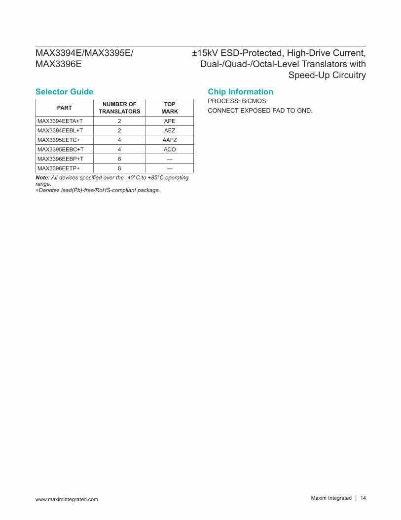
Selector Guide appears at end of data sheet.
Note: All devices specified over the -40°C to +85°C operating range.+Denotes lead(Pb)-free/RoHS-compliant package. *Future product—contact factory for availability. **EP = Exposed paddle.
PART PIN-PACKAGE PKG CODEMAX3394EETA+T 8 TDFN-EP** T833-1MAX3394EEBL+T 9 UCSP B9-5MAX3395EETC+ 12 TQFN-EP** T1244-4MAX3395EEBC+T 12 UCSP B12-1MAX3396EEBP+T* 20 UCSP B20-1MAX3396EETP+* 20 TQFN-EP** T2055-4
1 2 3 4
8 7 6 5
V L I/O V
L1
I/O V
L2
GND
*CONNECT EXPOSED PAD TO GROUND
*EP
I/O V
CC2
I/O V
CC1ENV CC
MAX3394E
TDFN
TOP VIEW (LEADS ON BOTTOM)
+
Pin Configurations continued at end of data sheet.
MAX3394E/MAX3395E/MAX3396E
±15kV ESD-Protected, High-Drive Current, Dual-/Quad-/Octal-Level Translators with
Speed-Up Circuitry
Pin Configurations
Ordering Information
(All voltages referenced to GND.)VCC ..........................................................................-0.3V to +6VVL ............................................................................-0.3V to +6VI/O VCC_ ......................................................-0.3V to VCC + 0.3VI/O VL_ ........................................................... -0.3V to VL + 0.3VEN............................................................................-0.3V to +6VShort-Circuit Duration I/O VL_, I/O VCC_ to GND .....ContinuousMaximum Continuous Current..........................................±50mAContinuous Power Dissipation (TA = +70°C)
8-Pin TDFN (derate 18.2mW/°C above +70°C) ........1455mW 9-Bump UCSP (derate 4.7mW/°C above +70°C) ........379mW
12-Pin TQFN (derate 16.9mW/°C above +70°C) ......1349mW 12-Bump UCSP (derate 6.5mW/°C above +70°C) ......519mW 20-Pin TQFN (derate 20.8mW/°C above +70°C) ......1667mW 20-Bump UCSP (derate 10.0mW/°C above +70°C) ....800mW
Operating Temperature Range ........................... -40°C to +85°CStorage Temperature Range ............................ -65°C to +150°CJunction Temperature ......................................................+150°CBump Temperature (soldering) ........................................+235°CLead Temperature (soldering, 10s) .................................+300°C
(VCC = +1.65V to +5.5V, VL = +1.2V to VCC; CIOVL ≤ 15pF, CIOVCC ≤ 15pF; TA = -40°C to +85°C, unless otherwise noted. Typical values are at TA = +25°C.) (Note 1)
PARAMETER SYMBOL CONDITIONS MIN TYP MAX UNITSPOWER SUPPLYVL Supply Range VL 1.2 VCC V
VCC Supply Range VCC 1.65 5.50 V
Supply Current from VCC ICC I/O lines internally pulled up
MAX3394E 150
µAMAX3395E 300
MAX3396E 600
Supply Current from VL IL I/O lines internally pulled up
MAX3394E 30
µAMAX3395E 30
MAX3396E 30
VCC Tri-State Supply Current ICC-3 EN = GND, TA = +25°C 3 6 µA
VL Tri-State Supply Current IL-3 EN = GND, TA = +25°C 0.7 2 µA
LOGIC I/OI/O VL_ Input-Voltage High Threshold VIHL
0.7 x VL
V
I/O VL_ Input-Voltage Low Threshold VILL
0.3 x VL
V
I/O VL_ Internal Pullup DC Resistance RL EN = VCC or VL 5 10 20 kΩ
I/O VL_ Source Current During Low-to-High Transition IIHL VL = +1.2V 15 mA
I/O VL_ Sink Current During High-to-Low Transition IILL VCC = +1.65V 10 mA
MAX3394E/MAX3395E/MAX3396E
±15kV ESD-Protected, High-Drive Current, Dual-/Quad-/Octal-Level Translators with
Speed-Up Circuitry
www.maximintegrated.com Maxim Integrated 2
Absolute Maximum Ratings
Stresses beyond those listed under “Absolute Maximum Ratings” may cause permanent damage to the device. These are stress ratings only, and functional operation of the device at these or any other conditions beyond those indicated in the operational sections of the specifications is not implied. Exposure to absolute maximum rating conditions for extended periods may affect device reliability.
Electrical Characteristics

(VCC = +1.65V to +5.5V, VL = +1.2V to VCC; CIOVL ≤ 15pF, CIOVCC ≤ 15pF; TA = -40°C to +85°C, unless otherwise noted. Typical values are at TA = +25°C.) (Note 1)
PARAMETER SYMBOL CONDITIONS MIN TYP MAX UNITSI/O VL_ Low-to-High Transition Threshold VL-TH VCC = +3.3V, VL = +1.8V 0.3 x
VL
0.5 x VL
V
I/O VL_ Output-Voltage Low VOLL
I/O VL_ sink current = 5mA, VILC = 0V 0.25VI/O VL_ sink current = 10mA, VILC ≤ 0.4V or
0.2 x VL
VILC + 0.4V
I/O VL_ Tri-State Output Leakage Current EN = GND, TA = +25°C -1 +1 µA
I/O VCC_ Input-Voltage High Threshold VIHC (Note 2) 0.7 x
VCCV
I/O VCC_ Input-Voltage Low Threshold VILC (Note 2) 0.3 x
VCCV
I/O VCC_ Internal Pullup DC Resistance RCC EN = VCC or VL 5 10 20 kΩ
I/O VCC_ Source Current During Low-to-High Transition IIHCC VCC = +1.65V 15 mA
I/O VCC_ Sink Current During High-to-Low Transition IILCC VCC = +1.65V 10 mA
I/O VCC_ Low-to-High Transition Threshold VCC-TH VCC = +3.3V, VL = +1.8V 0.3 x
VCC
0.5 x VCC
V
I/O VCC_ Output-Voltage Low VOLC
I/O VCC_ sink current = 5mA, VILL = 0V 0.25VI/O VCC_ sink current = 10mA, VILL ≤ 0.4V
or 0.2 x VL
VILL + 0.4V
I/O VCC_ Tri-State Output Leakage Current EN = GND, TA = +25°C -1 +1 µA
EN Input-Voltage High Threshold VIHE0.7 x VL
V
EN Input-Voltage Low Threshold VILE0.3 x VL
V
EN Pin Input Leakage Current TA = +25°C -1 +1 µA
ESD PROTECTIONI/O VCC_ ESD Protection CVCC = 1µF, Human Body Model ±15 kV
MAX3394E/MAX3395E/MAX3396E
±15kV ESD-Protected, High-Drive Current, Dual-/Quad-/Octal-Level Translators with
Speed-Up Circuitry
www.maximintegrated.com Maxim Integrated 3
Electrical Characteristics (continued)
(VCC = +1.65V to +5.5V, VL = +1.2V to VCC; CIOVL ≤ 15pF, CIOVCC ≤ 15pF; TA = -40°C to +85°C, unless otherwise noted. Typical values are at TA = +25°C.) (Note 1)
Note 1: All units are 100% production tested at TA = +25°C. Limits over the operating temperature range are guaranteed by design and not production tested.
Note 2: During a low-to-high transition, the threshold at which the I/O changes state is the lower of VILL and VILC since the two sides are internally connected by an internal switch while the device is in the logic-low state.
PARAMETER SYMBOL CONDITIONS MIN TYP MAX UNITS
I/O VCC_ Rise Time tRVCCPush-pull driver, Figure 1 50
nsOpen-drain driver, internal pullup, Figure 2 500
I/O VCC_ Fall Time tFVCCPush-pull driver, Figure 1 50
nsOpen-drain driver, internal pullup, Figure 2 50
I/O VL_ Rise Time tRVLPush-pull driver, Figure 3 50
nsOpen-drain driver, internal pullup, Figure 4 500
I/O VL_ Fall Time tFVLPush-pull driver, Figure 3 50
nsOpen-drain driver, internal pullup, Figure 4 50
Propagation Delay
tI/OVL-VCCPush-pull driver, Figure 1 50
nsOpen-drain driver, internal pullup, Figure 2 600
tI/OVCC-VLPush-pull driver, Figure 3 50
Open-drain driver, internal pullup, Figure 4 600
Propagation Delay After EN tEN Push-pull or open-drain driver, Figure 5 5 µs
Channel-to-Channel Skew tSKEWPush-pull driver 5
nsOpen-drain driver, internal pullup 100
Maximum Data RatePush-pull driver, Figures 1, 3 6
MbpsOpen-drain driver, internal pullup,Figures 2, 4 1
MAX3394E/MAX3395E/MAX3396E
±15kV ESD-Protected, High-Drive Current, Dual-/Quad-/Octal-Level Translators with
Speed-Up Circuitry
www.maximintegrated.com Maxim Integrated 4
Timing Characteristics

(VCC = +2.5V, VL = +1.8V, CL = 15pF, TA = +25°C, unless otherwise noted.)
VL SUPPLY CURRENTvs. SUPPLY VOLTAGE
MAX
3394
E–96
E to
c02
VL SUPPLY VOLTAGE (V)
V L S
UPPL
Y CU
RREN
T (m
A)
4.54.03.53.02.52.0
0.5
1.0
1.5
2.0
2.5
3.0
01.5 5.0
VCC = +5.0VDRIVING I/O VL_
1Mbps OPEN-DRAIN
6Mbps PUSH-PULL
VCC SUPPLY CURRENTvs. TEMPERATURE
MAX
3394
E–96
E to
c03
TEMPERATURE (°C)
V CC
SUPP
LY C
URRE
NT (m
A)
603510-15
0.1
0.2
0.3
0.4
0.5
0.6
0.7
0.8
0.9
1.0
0-40 85
DRIVING I/O VL_
1Mbps OPEN-DRAIN
6Mbps PUSH-PULL
VL SUPPLY CURRENTvs. TEMPERATURE
MAX
3394
E–96
E to
c04
TEMPERATURE (°C)
V L S
UPPL
Y CU
RREN
T (m
A)
603510-15
0.05
0.10
0.15
0.20
0.25
0.30
0.35
0-40 85
DRIVING I/O VL_
1Mbps OPEN-DRAIN
6Mbps PUSH-PULL
0
1.5
1.0
0.5
2.0
2.5
3.0
0 403010 20 50 60 70 80 90 100
MAX
3394
E-96
E to
c05
LOAD CAPACITANCE (pF)
V CC
SUPP
LY C
URRE
NT (m
A)
VCC SUPPLY CURRENTvs. LOAD CAPACITANCE
DRIVING I/O VL_
6Mbps PUSH-PULL
1Mbps OPEN-DRAIN0
0.2
0.1
0.4
0.3
0.6
0.5
0.7
0.9
0.8
1.0
0 20 30 4010 50 60 70 9080 100
MAX
3394
E-96
E to
c06
LOAD CAPACITANCE (pF)
V L S
UPPL
Y CU
RREN
T (m
A)
VL SUPPLY CURRENTvs. LOAD CAPACITANCE
DRIVING I/O VL_
6Mbps PUSH-PULL
1Mbps OPEN-DRAIN
0
100
50
200
150
300
250
350
450
400
500
0 20 30 4010 50 60 70 9080 100
MAX
3394
E-96
E to
c07
CAPACITIVE LOAD (pF)
RISE
TIM
E (n
s)
OPEN-DRAIN RISE TIMEvs. LOAD CAPACITANCE
DRIVING I/O VL_
DRIVING I/O VCC_
VCC SUPPLY CURRENTvs. SUPPLY VOLTAGE
MAX
3394
E–96
E to
c01
VCC SUPPLY VOLTAGE (V)
V CC
SUPP
LY C
URRE
NT (m
A)
5.04.54.03.53.02.52.0
0.5
1.0
1.5
2.0
2.5
3.0
01.5 5.5
VL = +1.2VDRIVING I/O VL_
1Mbps OPEN-DRAIN
6Mbps PUSH-PULL
OPEN-DRAIN FALL TIMEvs. LOAD CAPACITANCE
MAX
3394
E–96
E to
c08
LOAD CAPACITANCE (pF)
FALL
TIM
E (n
s)
908070605040302010
5
10
15
20
25
30
00 100
DRIVING I/O VCC_
DRIVING I/O VL_
PUSH-PULL RISE TIMEvs. LOAD CAPACITANCE
MAX
3394
E–96
E to
c09
LOAD CAPACITANCE (pF)
RISE
TIM
E (n
s)
908070605040302010
5
10
15
20
25
30
00 100
DRIVING I/O VCC_
DRIVING I/O VL_
MAX3394E/MAX3395E/MAX3396E
±15kV ESD-Protected, High-Drive Current, Dual-/Quad-/Octal-Level Translators with
Speed-Up Circuitry
Maxim Integrated 5www.maximintegrated.com
Typical Operating Characteristics

(VCC = +2.5V, VL = +1.8V, CL = 15pF, TA = +25°C, unless otherwise noted.)
0
4
2
8
6
12
10
14
0 4020 60 8010 5030 70 90 100
MAX
3394
E-96
E to
c10
LOAD CAPACITANCE (pF)
FALL
TIM
E (n
s)
PUSH-PULL FALL TIMEvs. LOAD CAPACITANCE
DRIVING I/O VL_
DRIVING I/O VCC_
0
15
10
5
20
25
30
0 403010 20 50 60 70 80 90 100
PROPAGATION DELAYvs. LOAD CAPACITANCE
MAX
3394
E-96
E to
c11
LOAD CAPACITANCE (pF)
PROP
AGAT
IN D
ELAY
(ns)
DRIVING I/O VL_ OPEN-DRAIN
tPDHL
tPDLH
0
4
2
8
6
12
10
14
18
16
20
0 20 30 4010 50 60 70 9080 100
MAX
3394
E-96
E to
c12
LOAD CAPACITANCE (pF)
PROP
AGAT
ION
DELA
Y (n
s)
DRIVING I/O VCC_ OPEN-DRAIN
PROPAGATION DELAYvs. LOAD CAPACITANCE
tPDHL
tPDLH
PROPAGATION DELAYvs. LOAD CAPACITANCE
MAX
3394
E–96
E to
c13
LOAD CAPACITANCE (pF)
PROP
AGAT
ION
DELA
Y (n
s)
908060 7020 30 40 5010
5
10
15
20
25
30
35
40
45
50
00 100
tPDHL
DRIVING I/O VL_ PUSH-PULL
tPDLH
0
4
2
8
6
12
10
14
18
16
20
0 20 30 4010 50 60 70 9080 100
MAX
3394
E-96
E to
c14
LOAD CAPACITANCE (pF)
PROP
AGAT
ION
DELA
Y (n
s)
DRIVING I/O VCC_ PUSH-PULLSEE FIGURE 3
PROPAGATION DELAYvs. LOAD CAPACITANCE
tPDHL
40ns/div
(DRIVING I/O VL_, VCC = +2.5V, VL = +1.8V, CL = 15pF, DATA RATE = 6Mbps)
I/O VCC_1V/div
I/O VL_ 1V/div
MAX3394E-96E toc15
200ns/div
(DRIVING I/O VL_, VCC = +5.0V, VL = +3.3V,CL = 100pF, DATA RATE = 1Mbps)
MAX3394E-96E toc16
I/O VCC_2V/div
I/O VL_ 2V/div
200ns/div
(DRIVING I/O VL_, VCC = +5.0V, VL = +3.3V,CL = 400pF, EXTERNAL 4.7kΩ
PULLUPS, DATA RATE = 1Mbps)MAX3394E-96E toc17
I/O VCC_2V/div
I/O VL_ 2V/div
MAX3394E/MAX3395E/MAX3396E
±15kV ESD-Protected, High-Drive Current, Dual-/Quad-/Octal-Level Translators with
Speed-Up Circuitry
Maxim Integrated 6www.maximintegrated.com
Typical Operating Characteristics (continued)

Detailed DescriptionThe MAX3394E/MAX3395E/MAX3396E bidirectional level translators provide level shifting required for data transfer in a multivoltage system. Internal slew-rate enhancement circuitry features 10mA current-sink and 15mA current-source drivers to isolate capacitive loads from lower cur-rent drivers. In open-drain systems, slew-rate enhance-ment enables fast data rates with larger pullup resistors
and increased bus load capacitance. Externally applied voltages, VCC and VL, set the logic-high levels for the device. A logic-low signal on one I/O side of the device appears as a logic-low signal on the opposite I/O side and vice-versa. Each I/O line is pulled up to VCC or VL by an internal pullup resistor, allowing the devices to be driven by either push-pull or open-drain drivers.
PINNAME FUNCTIONMAX3394E MAX3395E MAX3396E
TDFN UCSP TQFN UCSP TQFN UCSP
1 A1 11 B1 14 D3 VCC
VCC Supply Voltage +1.65V ≤ VCC ≤ +5.5V. Bypass VCC to GND with a 0.1µF ceramic capacitor and a 1µF or greater ceramic capacitor as close to the device as possible.
2 B1 6 B3 4 A4 EN
Enable Input. Drive EN logic high for normal operation. Drive EN logic low to force all I/O lines to a high-impedance state and disconnect internal pullup resistors.
3 A2 10 C1 18 C1 I/O VCC1 I/O 1 Referred to VCC4 A3 9 C2 16 D1 I/O VCC2 I/O 2 Referred to VCC5 B3 5 B4 13 D4 GND Ground
6 C3 2 A2 20 A1 I/O VL2 I/O 2 Referred to VL7 C2 1 A1 19 B1 I/O VL1 I/O 1 Referred to VL
8 C1 12 B2 3 A3 VL
Logic Supply Voltage +1.2V ≤ VL ≤ VCC. Bypass VL to GND with a 0.1µF or greater ceramic capacitor as close to the device as possible.
— — 3 A3 1 B2 I/O VL3 I/O 3 Referred to VL— — 4 A4 2 A2 I/O VL4 I/O 4 Referred to VL— — 7 C4 15 D2 I/O VCC4 I/O 4 Referred to VCC— — 8 C3 17 C2 I/O VCC3 I/O 3 Referred to VCC— — — — 12 C3 I/O VCC5 I/O 5 Referred to VCC— — — — 11 D5 I/O VCC6 I/O 6 Referred to VCC— — — — 10 C4 I/O VCC7 I/O 7 Referred to VCC— — — — 9 C5 I/O VCC8 I/O 8 Referred to VCC— — — — 5 B3 I/O VL5 I/O 5 Referred to VL— — — — 6 A5 I/O VL6 I/O 6 Referred to VL— — — — 7 B4 I/O VL7 I/O 7 Referred to VL— — — — 8 B5 I/O VL8 I/O 8 Referred to VLEP — EP — EP — EP Exposed Pad. Connect exposed pad to GND.
MAX3394E/MAX3395E/MAX3396E
±15kV ESD-Protected, High-Drive Current, Dual-/Quad-/Octal-Level Translators with
Speed-Up Circuitry
www.maximintegrated.com Maxim Integrated 7
Pin Description

The MAX3394E/MAX3395E/MAX3396E feature a tri-state output mode, thermal-shutdown protection, and ±15kV Human Body Model (HBM) ESD protection on the VCC side for greater protection in applications that route signals externally.The MAX3394E/MAX3395E/MAX3396E accept VCC volt-ages from +1.65V to +5.5V, and VL voltages from +1.2V to VCC, making them ideal for data transfer between low-voltage ASIC/PLDs and higher voltage systems. The MAX3394E/MAX3395E/MAX3396E operate at a guaran-
teed data rate of 6Mbps with push-pull drivers and 1Mbps with open-drain drivers.
Level TranslationThe MAX3394E/MAX3395E/MAX3396E utilize a trans-mission gate architecture to provide bidirectional level translation between I/O VL_ and I/O VCC_. The trans-mission gate architecture is comprised of a pass-FET, gate-control logic, and slew-rate enhancement circuitry. When both I/O VL_ and I/O VCC_ are logic high, the gate-control logic disables the pass-FET, providing
Figure 1. Push-Pull Driving I/O VL_Test Circuit and Timing
Figure 2. Open-Drain Driving I/O VL_ Test Circuit and Timing
MAX3394EMAX3395EMAX3396E
tFVCCtRVCC
tI/OVL-VCC
I/O VL_ I/O VCC_
50Ω
VL
VL VCC
10%10%
90%90%
50% 50%
50%50%
VCC
CIOVCC
tI/OVL-VCC
VCCENVL
I/O VCC
I/O VL
MAX3394EMAX3395EMAX3396E
tFVCCtRVCC
tI/OVL-VCC
I/O VL_ I/O VCC_
VL
VL VCC
10%10%
90%90%
50% 50%
50%50%
VCC
CIOVCC
tI/OVL-VCC
I/O VCC
VGATE
VL VCCEN
VGATE
MAX3394E/MAX3395E/MAX3396E
±15kV ESD-Protected, High-Drive Current, Dual-/Quad-/Octal-Level Translators with
Speed-Up Circuitry
www.maximintegrated.com Maxim Integrated 8

capacitive isolation between I/O lines. When one or both I/O lines are at a logic-low level, the gate-control logic turns the pass-FET on. When the pass-FET is active, I/O VL_ and I/O VCC_ are connected, allowing the logic-low signal to be expressed simultaneously on both I/O lines.The MAX3394E/MAX3395E/MAX3396E have internal 10kΩ (typ) pullup resistors from I/O VL_ and I/O VCC_ to the respective supply voltages, allowing operation with open-drain drivers. Internal slew-rate enhancement circuitry accelerates logic-state transitions, maintain-ing a fast data rate with a higher bus load capacitance. Additionally, the 10mA current sink drivers permit the use of smaller external pullup resistors.
Internal Slew-Rate EnhancementInternal slew-rate enhancement circuitry accelerates log-ic-state changes by turning on MOSFETs MP1 and MP2 during low-to-high logic transitions, and MOSFETs MN3 and MN4 during high-to-low logic transitions (see the Functional Diagram). During logic-state changes, speed-up MOSFETS are triggered by I/O line voltage thresholds. MOSFETS MN3 and MN4 sink 10mA during high-to-low logic transitions. MP1 and MP2 source 15mA during low-to-high logic transitions. Slew-rate enhancement allows a fast data rate despite large capacitive bus loads, and permits larger external pullup resistors.
Figure 3. Push-Pull Driving I/O VCC_ Test Circuit and Timing
Figure 4. Open-Drain Driving I/O VCC_ Test Circuit and Timing
MAX3394EMAX3395EMAX3396E
tFVLtRVL
tI/OVCC-VL
I/O VL_ I/O VCC_
VL
VL VCC
10%10%
90%90%
50% 50%
50%50%VCC
CIOVL
tI/OVCC-VL
I/O VCCVL VCCEN
50ΩI/O VL
MAX3394EMAX3395EMAX3396E
tI/OVCC-VL
I/O VL_ I/O VCC_
VL
VL VCC
10%10%
90%90%
50% 50%
50%50%VCC
CIOVLtI/OVCC-VL
I/O VL
VL VCCEN
tFVLtRVL
VGATE
MAX3394E/MAX3395E/MAX3396E
±15kV ESD-Protected, High-Drive Current, Dual-/Quad-/Octal-Level Translators with
Speed-Up Circuitry
www.maximintegrated.com Maxim Integrated 9

Power-Supply SequencingThe MAX3394E/MAX3395E/MAX3396E require two sup-ply voltages. For proper operation, ensure that +1.65V ≤ VCC ≤ +5.5V, and +1.2V ≤ VL ≤ VCC. There are no restric-tions on power-supply sequencing. During power-up or power-down, the MAX3394E/MAX3395E/MAX3396E can withstand either the VL or the VCC supply floating while the other supply is applied. The device will not latch up in this state.
Tri-State Output ModeConnect EN to VL or VCC for normal operation. Drive EN low to force the MAX3394E/MAX3395E/MAX3396E to a tri-state output mode. In tri-state output mode, all I/O lines are driven to a high-impedance state, and the pass-FET is disabled to prevent current flow between I/O lines. Tri-state output mode disables the internal pullup resistors on I/O VL_ and I/O VCC_, and reduces supply current to 3μA typ (VCC) and 0.7μA typ (VL).
Figure 5. Enable Test Circuit and Timing
MAX3394EMAX3395EMAX3396E
I/O VL_ I/O VCC_
VL
VL VCC
VCC
VL VCCEN
50Ω
RLOAD
CIOVCC
MAX3394EMAX3395EMAX3396E
I/O VCC_
VL
VL VCC
VCC
VL VCCEN
50Ω
RLOAD
I/O VL_
EN
EN
TIME
TIME
tEN
tEN
I/O VCC_V
I/O VL_
V
CIOVL
0.5V
0.2V (VL < 2V)0.5V (VL 2V)
MAX3394E/MAX3395E/MAX3396E
±15kV ESD-Protected, High-Drive Current, Dual-/Quad-/Octal-Level Translators with
Speed-Up Circuitry
www.maximintegrated.com Maxim Integrated 10

The high-impedance state of the I/O lines during tri-state output mode facilitates use in multidrop networks. In tri-state output mode, do not exceed (VL + 0.3V) on I/O VL_ or (VCC + 0.3V) on I/O VCC_.
Thermal-Shutdown ProtectionThe MAX3394E/MAX3395E/MAX3396E are protected from thermal damage resulting from short-circuit faults. In the event of a short-circuit fault, when the junction tem-perature (TJ) reaches +125°C, a thermal sensor forces the device into the tri-state output mode. When TJ drops below +115°C, normal operation resumes.
±15kV ESD ProtectionAs with all Maxim devices, ESD-protection structures are incorporated on all pins to protect against ESD encoun-tered during handling and assembly. The I/O VCC_ lines are further protected by advanced ESD structures to guard these pins from damage caused by ESD of up to ±15kV. Protection structures prevent damage caused by ESD events in normal operation, tri-state output mode, and when the device is unpowered. After arresting an ESD event, MAX3394E/MAX3395E/MAX3396E continue to function without latching up, whereas competing devic-es can enter a latched-up state and must be power cycled to restore functionality.Several ESD testing standards exist for gauging the robustness of ESD structures. The ESD protection of the MAX3394E/MAX3395E/MAX3396E is characterized for the human body model (HBM). Figure 6a shows the model used to simulate an ESD event resulting from con-tact with the human body. The model consists of a 100pF storage capacitor that is charged to a high voltage then discharged through a 1.5kΩ resistor. Figure 6b shows the current waveform when the storage capacitor is dis-charged into a low impedance.
To ensure full ±15kV ESD protection, bypass VCC to ground with a 0.1μF ceramic capacitor and an additional 1μF ceramic capacitor as close to the device as possible.
ESD Test ConditionsESD performance depends on a variety of conditions. Contact Maxim for a reliability report documenting test setup, methodology, and results.
Applications InformationPower-Supply DecouplingBypass VL and VCC to ground with 0.1μF ceramic capac-itors. To ensure full ±15kV ESD protection, bypass VCC to ground with an additional 1μF or greater ceramic capaci-tor. Place all capacitors as close to the device as possible.
Open-Drain Mode vs. Push-Pull ModeThe MAX3394E/MAX3395E/MAX3396E are compatible with push-pull (active) and open-drain drivers. For push-pull operation, maximum data rate is guaranteed to 6Mbps. For open-drain applications, the MAX3394E/MAX3395E/MAX3396E include internal pullup resistors and slew-rate enhancement circuitry, providing a maxi-mum data rate of 1Mbps. External pullup resistors can be added to increase data rate when the bus is loaded by high capacitance. (See the Use of External Pullup Resistors section.)
Serial-Interface Level TranslationThe MAX3395E provides level translation on four I/O lines, making it an ideal device for multivoltage I2C, MICROWIRE, and SPI serial interfaces.
Use of External Pullup ResistorsThe MAX3394E/MAX3395E/MAX3396E include internal 10kΩ pullup resistors. During a low-to-high logic transi-tion, the internal pullup resistors charge the bus capaci-
Figure 6a. Human Body ESD Test Model Figure 6b. HBM Discharge Current Waveform
CHARGE-CURRENT-LIMIT RESISTOR
DISCHARGERESISTANCE
STORAGECAPACITOR
Cs100pF
RC1MΩ
RD 1500Ω
HIGH-VOLTAGE
DCSOURCE
DEVICE-UNDER-
TEST
IP 100%90%
36.8%
tRLTIME
tDLCURRENT WAVEFORM
PEAK-TO-PEAK RINGING(NOT DRAWN TO SCALE)
Ir
10%0
0
AMPERES
MAX3394E/MAX3395E/MAX3396E
±15kV ESD-Protected, High-Drive Current, Dual-/Quad-/Octal-Level Translators with
Speed-Up Circuitry
www.maximintegrated.com Maxim Integrated 11

tance with a characteristic RC charging waveform. When the low-to-high transition threshold (VCC-TH or VLTH) is reached, the rise time accelerators switch on, sourcing 15mA to fully charge the bus capacitance. External pullup resistors reduce the time needed to reach the low-to-high transition threshold, thereby increasing the data rate. In the logic-low state however, external pullup resistors increase the DC current through the internal pass-FET, increasing the output voltage of the device.
Smart-Card InterfaceThe MAX3395E provides level translation for Class A, B, and C smart cards. When supply voltage VCC is inter-rupted due to the disconnection of a smart card, the
device does not latch up. Normal operation resumes upon restoration of the VCC supply voltage. The MAX3395E provides bidirectional level translation on four I/O lines, making it well suited for buffering and translating 4-wire serial interfaces.
UCSP Applications InformationFor the latest application details on UCSP construction, dimensions, tape carrier information, PCB techniques, bump-pad layout, and recommended reflow temperature profiles, as well as the latest information on reliability testing results, go to Maxim’s web site at www.maximin-tegrated.com/ucsp to find the Application Note 1891: Wafer-Level Packaging (WLP) and Its Applications.
GND GND GND
+1.8VSYSTEM
CONTROLLER
+3.3VSYSTEM
VL VCC
I/O VL1I/O VL2
I/O VCC1I/O VCC2
CLKDATA
CLK DATA
+3.3V+1.8V
ENEN
0.1µF 1µF0.1µF
MAX3394E
MP2MP1
MN4MN3
GATE CONTROL
SLEW-RATEENHANCEMENT
N-CHANNELPASS-FET
I/O VL_ I/O VCC_
VL VCC
VL VCC
MAX3394E/MAX3395E/MAX3396E
±15kV ESD-Protected, High-Drive Current, Dual-/Quad-/Octal-Level Translators with
Speed-Up Circuitry
www.maximintegrated.com Maxim Integrated 12
Functional Diagram
Typical Operating Circuit

1 2 3
A
B
C
UCSP
UCSP
A
B
C
1 2 3 4
12VL
11VCC
10I/O VCC1
4
5 GND
6 EN
1 2
I/O V
L2
3
9 8 7
I/O V
L3
I/O V
CC2
I/O V
CC3
I/O V
CC4
MAX3395E
I/O V
L1
I/O VL4
TQFN
TOP VIEW(BUMPS ON BOTTOM)
MAX3394E
VCC I/O VCC1 I/O VCC2
I/O VL1 I/O VL2
EN GND
VL
I/O VL2 I/O VL4I/O VL1 I/O VL3
VL GNDVCC EN
MAX3395E
I/O VCC2 I/O VCC4I/O VCC1 I/O VCC3
*CONNECT EXPOSED PAD TO GROUND
*EP
+
19
20
18
17
7
6
8
I/O V
L4 EN
I/O V
L5
9
I/O V
L3
V CC
I/O V
CC5
I/O V
CC6
I/O V
CC4
1 2
I/O VCC1
4 5
15 14 12 11
I/O VL1
I/O VL2
I/O VCC8
I/O VL8
I/O VL7
I/O VL6
MAX3396E
V LGN
D
3
13
I/O VCC3
16 10 I/O VCC7I/O VCC2
TQFN*CONNECT EXPOSED PAD TO GROUND
*EP
+
UCSP
A
B
C
1 2 3 4
I/O VL4 ENI/O VL2 VL
I/O VL3 I/O VL7I/O VL1 I/O VL5
MAX3396E
I/O VCC3 I/O VCC7I/O VCC1 I/O VCC5
D
I/O VCC4 GNDI/O VCC2 VCC
5
I/O VL6
I/O VL8
I/O VCC8
I/O VCC6
TOP VIEW(LEADS ON BOTTOM)
TOP VIEW(BUMPS ON BOTTOM)
TOP VIEW(BUMPS ON BOTTOM)
TOP VIEW(LEADS ON BOTTOM)
MAX3394E/MAX3395E/MAX3396E
±15kV ESD-Protected, High-Drive Current, Dual-/Quad-/Octal-Level Translators with
Speed-Up Circuitry
www.maximintegrated.com Maxim Integrated 13
Pin Configurations (continued)
Note: All devices specified over the -40°C to +85°C operating range. +Denotes lead(Pb)-free/RoHS-compliant package.
PART NUMBER OF TRANSLATORS
TOPMARK
MAX3394EETA+T 2 APE
MAX3394EEBL+T 2 AEZ
MAX3395EETC+ 4 AAFZ
MAX3395EEBC+T 4 ACO
MAX3396EEBP+T 8 —
MAX3396EETP+ 8 —
MAX3394E/MAX3395E/MAX3396E
±15kV ESD-Protected, High-Drive Current, Dual-/Quad-/Octal-Level Translators with
Speed-Up Circuitry
www.maximintegrated.com Maxim Integrated 14
Selector Guide Chip InformationPROCESS: BiCMOSCONNECT EXPOSED PAD TO GND.

maxim integratedTM
COMMON DIMENSIONS
SYMBOL MIN MAX
A 0.70 0.80
D 2.90 3.10
E 2.90 3.10
A1 0.00 0.05
L 0.20 0.40
PKG. CODE N D2 E2 e JEDEC SPEC b [(N/2)-1] x e
PACKAGE VARIATIONS
0.25 MIN.k
A2 0.20 REF.
2.00 REF0.25±0.050.50 BSC2.30±0.1010T1033-1
2.40 REF0.20±0.05- - - -0.40 BSC1.70±0.10 2.30±0.1014T1433-1
1.50±0.10 MO229 / WEED-3
0.40 BSC - - - - 0.20±0.05 2.40 REFT1433-2 14 2.30±0.101.70±0.10
T633-2 6 1.50±0.10 2.30±0.10 0.95 BSC MO229 / WEEA 0.40±0.05 1.90 REF
T833-2 8 1.50±0.10 2.30±0.10 0.65 BSC MO229 / WEEC 0.30±0.05 1.95 REF
T833-3 8 1.50±0.10 2.30±0.10 0.65 BSC MO229 / WEEC 0.30±0.05 1.95 REF
2.30±0.10 MO229 / WEED-3 2.00 REF0.25±0.050.50 BSC1.50±0.1010T1033-2
0.25±0.05 2.00 REF10 0.50 BSC MO229 / WEED-32.30±0.101.50±0.10T1033MK-1
0.40 BSC - - - - 0.20±0.05 2.40 REFT1433-3F 14 2.30±0.101.70±0.10
T833-2C 8 1.50±0.10 2.30±0.10 0.65 BSC MO229 / WEEC 0.30±0.05 1.95 REF
2.00 REF0.25±0.050.50 BSC2.30±0.1010T1033-1C 1.50±0.10 MO229 / WEED-3
maxim integratedTM
T633MK-1 6 1.50±0.10 2.30±0.10 0.95 BSC MO229 / WEEA 0.40±0.05 1.90 REF
T633-2C 6 1.50±0.10 2.30±0.10 0.95 BSC MO229 / WEEA 0.40±0.05 1.90 REF
0.40 BSC - - - - 0.20±0.05 2.40 REFT1433-2C 14 2.30±0.101.70±0.10
T833-3C 8 1.50±0.10 2.30±0.10 0.65 BSC MO229 / WEEC 0.30±0.05 1.95 REF
NOM
0.75
3.00
3.00
0.025
0.30
2.30±0.10 MO229 / WEED-3 2.00 REF0.25±0.050.50 BSC1.50±0.1010T1033-4
T833-1F 8 1.50±0.10 2.30±0.10 0.65 BSC MO229 / WEEC 0.30±0.05 1.95 REF
MAX3394E/MAX3395E/MAX3396E
±15kV ESD-Protected, High-Drive Current, Dual-/Quad-/Octal-Level Translators with
Speed-Up Circuitry
www.maximintegrated.com Maxim Integrated 15
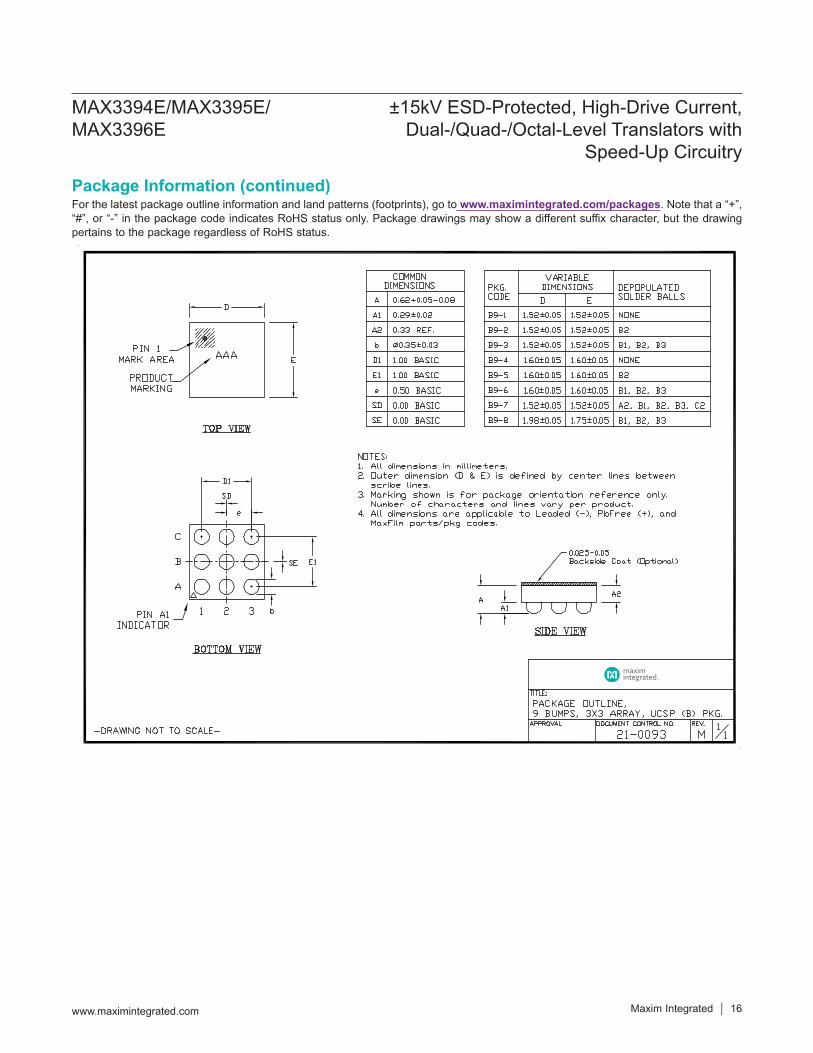
Package InformationFor the latest package outline information and land patterns (footprints), go to www.maximintegrated.com/packages. Note that a “+”, “#”, or “-” in the package code indicates RoHS status only. Package drawings may show a different suffix character, but the drawing pertains to the package regardless of RoHS status.
MAX3394E/MAX3395E/MAX3396E
±15kV ESD-Protected, High-Drive Current, Dual-/Quad-/Octal-Level Translators with
Speed-Up Circuitry
www.maximintegrated.com Maxim Integrated 16
Package Information (continued)For the latest package outline information and land patterns (footprints), go to www.maximintegrated.com/packages. Note that a “+”, “#”, or “-” in the package code indicates RoHS status only. Package drawings may show a different suffix character, but the drawing pertains to the package regardless of RoHS status.

e
E1
D1
b
SE SD
0.05 M S AB
B
A
E
D
Pin 1Indicator Marking see Note 7
A3
A2 A
A1
0.05 S
S
FRONT VIEW
TOP VIEW
BOTTOM VIEW
A1
0.640.240.40
0.0400.311.001.500.500.000.25
A
AAAA
SIDE VIEW
1 432
C
B
PKG. CODE
VARIABLE DIMENSIONS DEPOPULATED SOLDER BALLS
D EB12-1 1.54 0.05 2.02 0.05 NONEB12-2 1.54 0.05 2.02 0.05 B3B12-3 1.54 0.05 2.12 0.05 NONEB12-4 1.54 0.05 2.02 0.05 B2, B3B12-6 1.64 0.05 2.12 0.05 B3B12-7 1.54 0.05 2.02 0.05 B1, B3B12-8 1.54 0.05 2.02 0.05 B2B12-9 1.54 0.05 2.12 0.05 B2, B3B12-10 1.54 0.05 2.02 0.05 B1, B2, B3, B4B12-11 1.54 0.05 2.02 0.05 A2, C3
TITLE
DOCUMENT CONTROL NO. REV. 11
APPROVAL
COMMON DIMENSIONS
A
A2
A1
A3
b
E1
D1
e
SD
SE
0.050.03
0.03BASICREF
BASIC
NOTES:1. Terminal pitch is defined by terminal center to center value.2. Outer dimension is defined by center lines between scribe lines.3. All dimensions in millimeter.4. Marking shown is for package orientation reference only.5. Tolerance is ± 0.02 unless specified otherwise.6. All dimensions apply to PbFree (+) package codes only.7. Front - side finish can be either Black or Clear.
BASICBASIC
- DRAWING NOT TO SCALE - I
BASICBASIC
maxim integrated TM
21-0104
PACKAGE OUTLINE 12 BUMPSWLP PKG. 0.5 mm PITCH,
DEPOPULATED BUMPS:see table on left
MAX3394E/MAX3395E/MAX3396E
±15kV ESD-Protected, High-Drive Current, Dual-/Quad-/Octal-Level Translators with
Speed-Up Circuitry
www.maximintegrated.com Maxim Integrated 17
Package Information (continued)For the latest package outline information and land patterns (footprints), go to www.maximintegrated.com/packages. Note that a “+”, “#”, or “-” in the package code indicates RoHS status only. Package drawings may show a different suffix character, but the drawing pertains to the package regardless of RoHS status.

maxim integratedTM
maxim integratedTM
MAX3394E/MAX3395E/MAX3396E
±15kV ESD-Protected, High-Drive Current, Dual-/Quad-/Octal-Level Translators with
Speed-Up Circuitry
www.maximintegrated.com Maxim Integrated 18
Package Information (continued)For the latest package outline information and land patterns (footprints), go to www.maximintegrated.com/packages. Note that a “+”, “#”, or “-” in the package code indicates RoHS status only. Package drawings may show a different suffix character, but the drawing pertains to the package regardless of RoHS status.

maxim integratedTM
maxim integratedTM
MAX3394E/MAX3395E/MAX3396E
±15kV ESD-Protected, High-Drive Current, Dual-/Quad-/Octal-Level Translators with
Speed-Up Circuitry
www.maximintegrated.com Maxim Integrated 19
Package Information (continued)For the latest package outline information and land patterns (footprints), go to www.maximintegrated.com/packages. Note that a “+”, “#”, or “-” in the package code indicates RoHS status only. Package drawings may show a different suffix character, but the drawing pertains to the package regardless of RoHS status.

MAX3394E/MAX3395E/MAX3396E
±15kV ESD-Protected, High-Drive Current, Dual-/Quad-/Octal-Level Translators with
Speed-Up Circuitry
www.maximintegrated.com Maxim Integrated 20
Package Information (continued)For the latest package outline information and land patterns (footprints), go to www.maximintegrated.com/packages. Note that a “+”, “#”, or “-” in the package code indicates RoHS status only. Package drawings may show a different suffix character, but the drawing pertains to the package regardless of RoHS status.

Maxim Integrated cannot assume responsibility for use of any circuitry other than circuitry entirely embodied in a Maxim Integrated product. No circuit patent licenses are implied. Maxim Integrated reserves the right to change the circuitry and specifications without notice at any time. The parametric values (min and max limits) shown in the Electrical Characteristics table are guaranteed. Other parametric values quoted in this data sheet are provided for guidance.
Maxim Integrated and the Maxim Integrated logo are trademarks of Maxim Integrated Products, Inc.
MAX3394E/MAX3395E/MAX3396E
±15kV ESD-Protected, High-Drive Current, Dual-/Quad-/Octal-Level Translators with
Speed-Up Circuitry
© 2017 Maxim Integrated Products, Inc. 21
REVISION NUMBER
REVISIONDATE DESCRIPTION PAGES
CHANGED
3 7/17 Updated Electrical Characteristics table 2–3
For pricing, delivery, and ordering information, please contact Maxim Direct at 1-888-629-4642, or visit Maxim Integrated’s website at www.maximintegrated.com.