Littelfuse Esd Protection Design Guide.pdf
47
ESD PROTECTION DESIGN GUIDE: TVS DIODE ARRAYS ©2012 Littelfuse, Inc 1
Transcript of Littelfuse Esd Protection Design Guide.pdf
8/10/2019 Littelfuse Esd Protection Design Guide.pdf
http://slidepdf.com/reader/full/littelfuse-esd-protection-design-guidepdf 1/47
ESD PROTECTION DESIGN GUIDE: TVS DIODE ARRAYS
©2012 Littelfuse, Inc 1
8/10/2019 Littelfuse Esd Protection Design Guide.pdf
http://slidepdf.com/reader/full/littelfuse-esd-protection-design-guidepdf 2/47
ESD PROTECTION DESIGN GUIDE: TVS DIODE ARRAYS
©2012 Littelfuse, Inc 2
This guide was developed to help electronics designers navigate
selection of appropriate TVS Diode Array circuit protection components
for equipment interfaces such USB, HDMI, Ethernet, and keypad.
This document includes consideration factors, example circuits,
applicable standards, and recommended components.
Table of Contents
Introduction: ............................................................................................................................................................................ 3
TVS Diode Array (SPATM) Series Descriptions ....................................................................................................................... 4
General Purpose ESD Protection .......................................................................................................................................... 4
Low Capacitance ESD Protection ......................................................................................................................................... 7
Lightning Surge Protection ................................................................................................................................................... 9
EMI Filter Arrays with ESD Protection .................................................................................................................................. 11
TVS Diode Array Ordering Guide ........................................................................................................................................... 12
Application Specific Device Selection .................................... .................................... ................................... ......................... 14
USB1.1 ................................................................................................................................................................................ 14
USB2.0 ................................................................................................................................................................................ 15
USB3.0 (Two Device Solution) .............................................................................................................................................. 16
USB3.0 (Fully Integrated Solution) ........................................................................................................................................ 17
HDMI ................................................................................................................................................................................... 18
HDMI (includes protection for Ethernet and 5V power) ......................................................................................................... 19
Display Port .......................................................................................................................................................................... 20
DVI....................................................................................................................................................................................... 21
10/100/1000 Ethernet, Intra-building Lightning Immunity (GR-1089) ................................. .................................... ................. 22
10/100/1000 Ethernet, Inter-building Lightning Immunity (GR-1089)...................................................................................... 23
10/100/1000 Ethernet, Tertiary Only Lightning Immunity (General) ....................................................................................... 24
10/100/1000 Ethernet (ESD only) .......................................................................................................................................... 25
eSATA ................................................................................................................................................................................. 26
1394a/b ................................................................................................................................................................................ 27
LVDS (Low Voltage Differential Signaling) .................................... .................................... ................................... .................. 28
Audio (Speaker/Microphone) ................................................................................................................................................ 29
Analog Video ........................................................................................................................................................................ 30
Keypad/Push Buttons ........................................................................................................................................................... 31
SIM Socket .......................................................................................................................................................................... 32
RS-232 ................................................................................................................................................................................. 33
RS-485 ................................................................................................................................................................................. 34
CAN Bus .............................................................................................................................................................................. 35
LCD and Camera Interfaces (Mobile) .................................................................................................................................... 36
Appendix A ............................................................................................................................................................................. 37
SPA Package Outlines ........................................................................................................................................................ 37
8/10/2019 Littelfuse Esd Protection Design Guide.pdf
http://slidepdf.com/reader/full/littelfuse-esd-protection-design-guidepdf 3/47
ESD PROTECTION DESIGN GUIDE: TVS DIODE ARRAYS
©2012 Littelfuse, Inc 3
Introduction:Designers of today’s electronic devices have demanded more
functionality with greater flexibility and higher levels of user
interaction. These circumstances have helped in driving the
development of nanometer chipsets along with a multitude of
user interfaces or ports. The confluence of these two has made
electronic devices more susceptible to ESD and required the need
for a more robust solution.
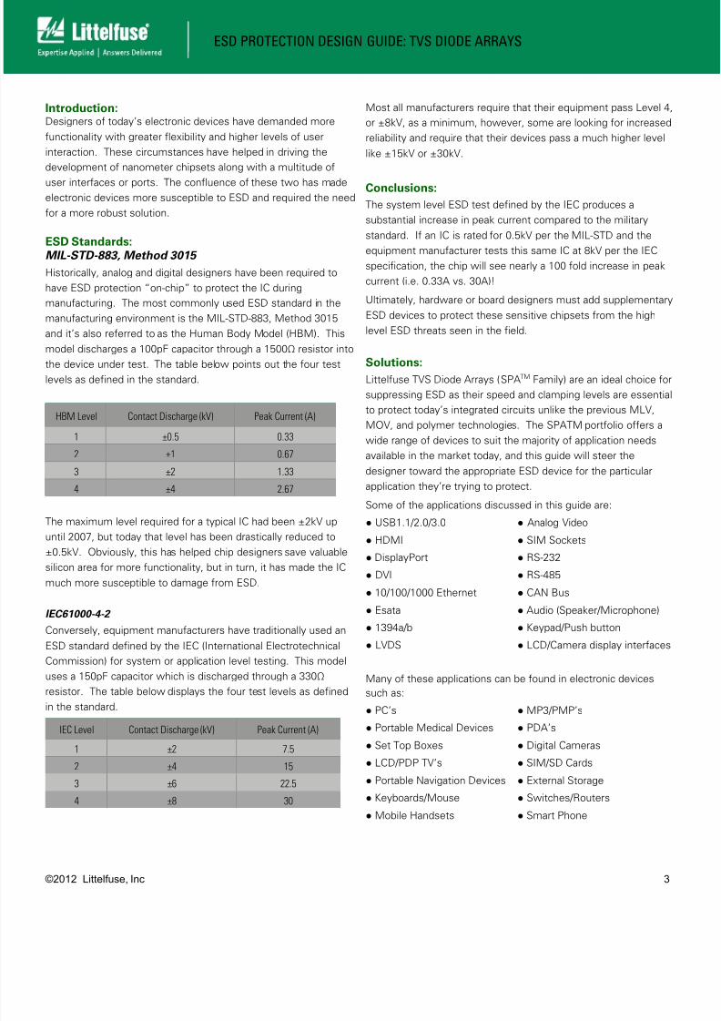
ESD Standards:MIL-STD-883, Method 3015
Historically, analog and digital designers have been required to
have ESD protection “on-chip” to protect the IC during
manufacturing. The most commonly used ESD standard in the
manufacturing environment is the MIL-STD-883, Method 3015
and it’s also referred to as the Human Body Model (HBM). This
model discharges a 100pF capacitor through a 1500Ω resistor into
the device under test. The table below points out the four test
levels as defined in the standard.
HBM Level Contact Discharge (kV) Peak Current (A)
1 ±0.5 0.33
2 ±1 0.67
3 ±2 1.33
4 ±4 2.67
The maximum level required for a typical IC had been ±2kV up
until 2007, but today that level has been drastically reduced to±0.5kV. Obviously, this has helped chip designers save valuable
silicon area for more functionality, but in turn, it has made the IC
much more susceptible to damage from ESD.
IEC61000-4-2
Conversely, equipment manufacturers have traditionally used an
ESD standard defined by the IEC (International Electrotechnical
Commission) for system or application level testing. This model
uses a 150pF capacitor which is discharged through a 330Ω
resistor. The table below displays the four test levels as defined
in the standard.
IEC Level Contact Discharge (kV) Peak Current (A)
1 ±2 7.5
2 ±4 15
3 ±6 22.5
4 ±8 30
Most all manufacturers require that their equipment pass Level 4,
or ±8kV, as a minimum, however, some are looking for increased
reliability and require that their devices pass a much higher level
like ±15kV or ±30kV.
Conclusions:
The system level ESD test defined by the IEC produces a
substantial increase in peak current compared to the military
standard. If an IC is rated for 0.5kV per the MIL-STD and the
equipment manufacturer tests this same IC at 8kV per the IEC
specification, the chip will see nearly a 100 fold increase in peak
current (i.e. 0.33A vs. 30A)!
Ultimately, hardware or board designers must add supplementary
ESD devices to protect these sensitive chipsets from the high
level ESD threats seen in the field.
Solutions:
Littelfuse TVS Diode Arrays (SPATM Family) are an ideal choice for
suppressing ESD as their speed and clamping levels are essential
to protect today’s integrated circuits unlike the previous MLV,
MOV, and polymer technologies. The SPATM portfolio offers a
wide range of devices to suit the majority of application needs
available in the market today, and this guide will steer the
designer toward the appropriate ESD device for the particular
application they’re trying to protect.
Some of the applications discussed in this guide are:
● USB1.1/2.0/3.0 ● Analog Video
● HDMI ● SIM Sockets
● DisplayPort ● RS-232
● DVI ● RS-485
● 10/100/1000 Ethernet ● CAN Bus
● Esata ● Audio (Speaker/Microphone)
● 1394a/b ● Keypad/Push button
● LVDS ● LCD/Camera display interfaces
Many of these applications can be found in electronic devices
such as:
● PC’s ● MP3/PMP’s● Portable Medical Devices ● PDA’s
● Set Top Boxes ● Digital Cameras
● LCD/PDP TV’s ● SIM/SD Cards
● Portable Navigation Devices ● External Storage
● Keyboards/Mouse ● Switches/Routers
● Mobile Handsets ● Smart Phone
8/10/2019 Littelfuse Esd Protection Design Guide.pdf
http://slidepdf.com/reader/full/littelfuse-esd-protection-design-guidepdf 4/47
ESD PROTECTION DESIGN GUIDE: TVS DIODE ARRAYS
©2012 Littelfuse, Inc 4
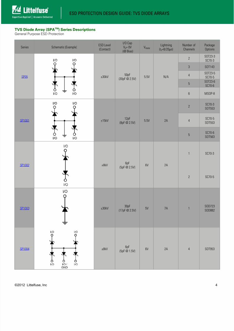
TVS Diode Array (SPATM) Series DescriptionsGeneral Purpose ESD Protection
Series Schematic (Example)ESD Level
(Contact)
I/O Cap
VR= 0V
(@ Bias)
VRWM Lightning
(tP=8/20μs)
Number of
Channels
Package
Options
SP05 ±30kV50pF
(30pF @ 2.5V)5.5V N/A
2 SOT23-3SC70-3
3 SOT143
4SOT23-5
SC70-5
5SOT23-6
SC70-6
6 MSOP-8
SP1001 ±15kV12pF
(8pF @ 2.5V)5.5V 2A
2SC70-3
SOT553
4SC70-5
SOT553
5SC70-6
SOT563
SP1002 ±8kV6pF
(5pF @ 2.5V)6V 2A
1 SC70-3
2 SC70-5
SP1003 ±30kV30pF
(17pF @ 2.5V)5V 7A 1
SOD723
SOD882
SP1004 ±8kV6pF
(5pF @ 1.5V)6V 2A 4 SOT953

8/10/2019 Littelfuse Esd Protection Design Guide.pdf
http://slidepdf.com/reader/full/littelfuse-esd-protection-design-guidepdf 5/47
ESD PROTECTION DESIGN GUIDE: TVS DIODE ARRAYS
©2012 Littelfuse, Inc 5
TVS Diode Arrays (SPATM) Series DescriptionsGeneral Purpose ESD Protection (continued)
Series Schematic (Example)ESD Level
(Contact)
I/O Cap
VR= 0V
(@ Bias)
VRWM Lightning
(tP=8/20μs)
Number of
Channels
Package
Options
SP1005 ±30kV30pF
(23pF @ 2.5V)6V 10A 1
0201
Flipchip
SP1006 ±30kV 25pF(15pF @ 2.5V)
6V 5A 1 0201μDFN-2
0.6x0.3mm
SP1007 ±8kV5pF
(3.5pF @ 5V)6V 2A 1
0201
Flipchip
SP1010 ±8kV6pF
(3.5pF @ 2.5V)6V 1A 4
μDFN-6
1.25x1.0mm
SP1011 ±15kV12pF
(7pF @ 2.5V)6V 2A 4
μDFN-6
1.25x1.0mm
8/10/2019 Littelfuse Esd Protection Design Guide.pdf
http://slidepdf.com/reader/full/littelfuse-esd-protection-design-guidepdf 6/47
ESD PROTECTION DESIGN GUIDE: TVS DIODE ARRAYS
©2012 Littelfuse, Inc 6
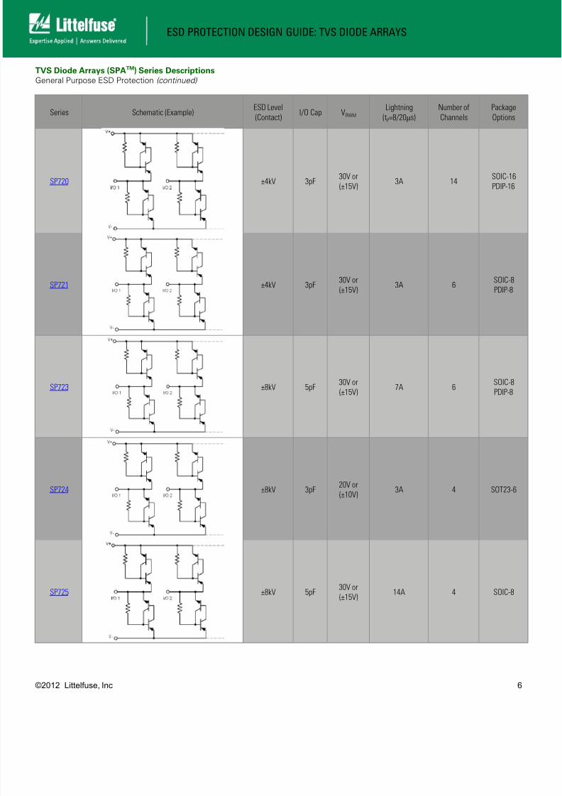
TVS Diode Arrays (SPATM) Series DescriptionsGeneral Purpose ESD Protection (continued)
Series Schematic (Example)ESD Level
(Contact)I/O Cap VRWM
Lightning
(tP=8/20μs)
Number of
Channels
Package
Options
SP720 ±4kV 3pF30V or
(±15V)3A 14
SOIC-16
PDIP-16
SP721 ±4kV 3pF 30V or(±15V)
3A 6 SOIC-8PDIP-8
SP723 ±8kV 5pF30V or
(±15V)7A 6
SOIC-8
PDIP-8
SP724 ±8kV 3pF20V or
(±10V)3A 4 SOT23-6
SP725 ±8kV 5pF30V or
(±15V)14A 4 SOIC-8
8/10/2019 Littelfuse Esd Protection Design Guide.pdf
http://slidepdf.com/reader/full/littelfuse-esd-protection-design-guidepdf 7/47
ESD PROTECTION DESIGN GUIDE: TVS DIODE ARRAYS
©2012 Littelfuse, Inc 7
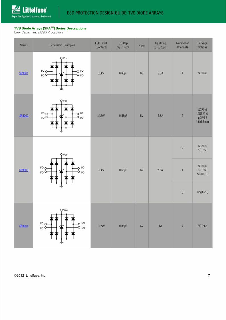
TVS Diode Arrays (SPATM) Series DescriptionsLow Capacitance ESD Protection
Series Schematic (Example)ESD Level
(Contact)
I/O Cap
VR= 1.65VVRWM
Lightning
(tP=8/20μs)
Number of
Channels
Package
Options
SP3001 ±8kV 0.65pF 6V 2.5A 4 SC70-6
SP3002 ±12kV 0.85pF 6V 4.5A 4
SC70-6
SOT23-6
μDFN-6
1.6x1.6mm
SP3003 ±8kV 0.65pF 6V 2.5A
2SC70-5
SOT553
4
SC70-6
SOT563
MSOP-10
8 MSOP-10
SP3004 ±12kV 0.85pF 6V 4A 4 SOT563
8/10/2019 Littelfuse Esd Protection Design Guide.pdf
http://slidepdf.com/reader/full/littelfuse-esd-protection-design-guidepdf 8/47
ESD PROTECTION DESIGN GUIDE: TVS DIODE ARRAYS
©2012 Littelfuse, Inc 8
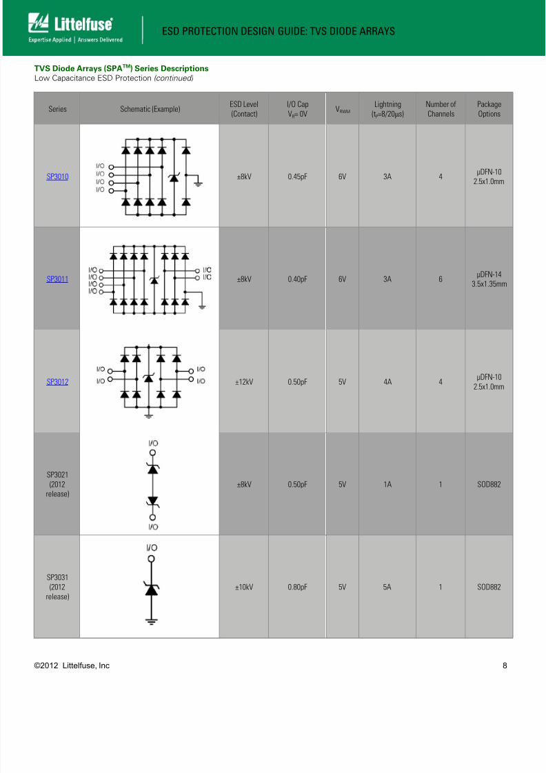
TVS Diode Arrays (SPATM) Series DescriptionsLow Capacitance ESD Protection (continued)
Series Schematic (Example)ESD Level
(Contact)
I/O Cap
VR= 0VVRWM
Lightning
(tP=8/20μs)
Number of
Channels
Package
Options
SP3010 ±8kV 0.45pF 6V 3A 4μDFN-10
2.5x1.0mm
SP3011 ±8kV 0.40pF 6V 3A 6μDFN-14
3.5x1.35mm
SP3012 ±12kV 0.50pF 5V 4A 4μDFN-10
2.5x1.0mm
SP3021
(2012
release)
±8kV 0.50pF 5V 1A 1 SOD882
SP3031
(2012
release)
±10kV 0.80pF 5V 5A 1 SOD882
8/10/2019 Littelfuse Esd Protection Design Guide.pdf
http://slidepdf.com/reader/full/littelfuse-esd-protection-design-guidepdf 9/47
ESD PROTECTION DESIGN GUIDE: TVS DIODE ARRAYS
©2012 Littelfuse, Inc 9
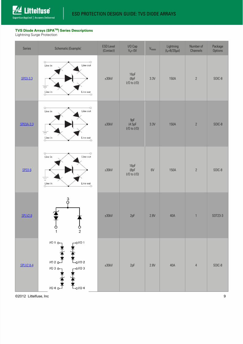
TVS Diode Arrays (SPATM) Series DescriptionsLightning Surge Protection
Series Schematic (Example)ESD Level
(Contact)
I/O Cap
VR= 0VVRWM
Lightning
(tP=8/20μs)
Number of
Channels
Package
Options
SP03-3.3 ±30kV
16pF
(8pF
I/O to I/O)
3.3V 150A 2 SOIC-8
SP03A-3.3 ±30kV9pF
(4.5pF
I/O to I/O)
3.3V 150A 2 SOIC-8
SP03-6 ±30kV
16pF
(8pF
I/O to I/O)
6V 150A 2 SOIC-8
SPLV2.8 ±30kV 2pF 2.8V 40A 1 SOT23-3
SPLV2.8-4 ±30kV 2pF 2.8V 40A 4 SOIC-8
8/10/2019 Littelfuse Esd Protection Design Guide.pdf
http://slidepdf.com/reader/full/littelfuse-esd-protection-design-guidepdf 10/47
ESD PROTECTION DESIGN GUIDE: TVS DIODE ARRAYS
©2012 Littelfuse, Inc 10
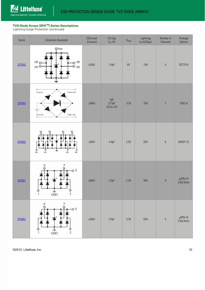
TVS Diode Arrays (SPATM) Series DescriptionsLightning Surge Protection (continued)
Series Schematic (Example)ESD Level
(Contact)
I/O Cap
VR= 0VVRWM
Lightning
(tP=8/20μs)
Number of
Channels
Package
Options
SP3050 ±20kV 2.4pF 6V 10A 4 SOT23-6
SP4040 ±30kV
5pF
(2.5pF
I/O to I/O)
3.3V 75A 2 SOIC-8
SP4060 ±30kV 4.4pF 2.5V 20A 8 MSOP-10
SP4061 ±30kV 3.5pF 2.5V 20A 4µDFN-10
2.6x2.6mm
SP4062 ±30kV 3.5pF 3.3V 20A 4µDFN-10
2.6x2.6mm
8/10/2019 Littelfuse Esd Protection Design Guide.pdf
http://slidepdf.com/reader/full/littelfuse-esd-protection-design-guidepdf 11/47
ESD PROTECTION DESIGN GUIDE: TVS DIODE ARRAYS
©2012 Littelfuse, Inc 11
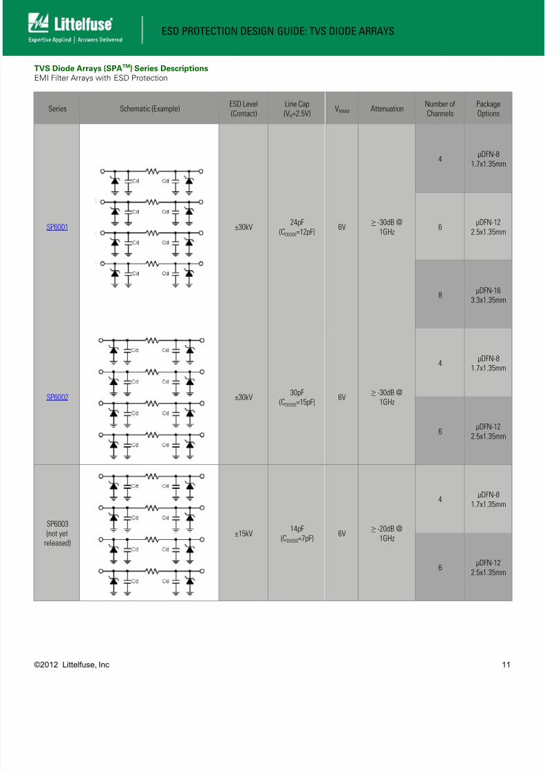
TVS Diode Arrays (SPATM) Series DescriptionsEMI Filter Arrays with ESD Protection
Series Schematic (Example)ESD Level
(Contact)
Line Cap
(VR=2.5V)VRWM Attenuation
Number of
Channels
Package
Options
SP6001 ±30kV24pF
(CDIODE=12pF)6V
≥ -30dB @
1GHz
4μDFN-8
1.7x1.35mm
6μDFN-12
2.5x1.35mm
8μDFN-16
3.3x1.35mm
SP6002 ±30kV30pF
(CDIODE=15pF)
6V≥ -30dB @
1GHz
4μDFN-8
1.7x1.35mm
6μDFN-12
2.5x1.35mm
SP6003
(not yet
released)
±15kV14pF
(CDIODE=7pF)
6V≥ -20dB @
1GHz
4μDFN-8
1.7x1.35mm
6μDFN-12
2.5x1.35mm
8/10/2019 Littelfuse Esd Protection Design Guide.pdf
http://slidepdf.com/reader/full/littelfuse-esd-protection-design-guidepdf 12/47
ESD PROTECTION DESIGN GUIDE: TVS DIODE ARRAYS
©2012 Littelfuse, Inc 12
TVS Diode Array Ordering Guide
Series Number of Channels Package Orderable Part Number
SP05
2SOT23-3 SP0502BAHTG
SC70-3 SP0502BAJTG
3 SOT143 SP0503BAHTG
4SOT23-5 SP0504BAHTG
SC70-5 SP0504BAJTG
5SOT23-6 SP0505BAHTG
SC70-6 SP0505BAJTG
6 MSOP-8 SP0506BAATG
SP1001
2SC70-3 SP1001-02JTG
SOT553 SP1001-02XTG
4 SC70-5 SP1001-04JTG
SOT553 SP1001-04XTG
5SC70-6 SP1001-05JTG
SOT56 SP1001-05XTG
SP1002 1 SC70-3 SP1002-01JTG
2 SC70-5 SP1002-02JTG
SP1003 1SOD723 SP1003-01DTG
SOD882 SP1003-01ETG
SP1004 4 SOT953 SP1004-04VTG
SP1005 1 0201 Flipchip SP1005-01WTG
SP1006 1 0201 (μDFN-2,0.6x0.3mm) SP1006-01UTG
SP1007 1 0201 Flipchip SP1007-01WTG
SP1010 4 μDFN-6 (1.25x1.0mm) SP1010-04UTG
SP1011 4 μDFN-6 (1.25x1.0mm) SP1011-04UTG
SP3001 4 SC70-6 SP3001-04JTG
SP3002 4
SOT23-6 SP3002-04HTG
SC70-6 SP3002-04JTG
μDFN-6 (1.6x1.6mm) SP3002-04UTG
SP3003
2SC70-5 SP3003-02JTG
SOT553 SP3003-02XTG
4
SC70-6 SP3003-04JTG
SOT563 SP3003-04XTG
MSOP-10 SP3003-04ATG
8 MSOP-10 SP3003-08ATG
SP3004 4 SOT563 SP3004-04XTG
8/10/2019 Littelfuse Esd Protection Design Guide.pdf
http://slidepdf.com/reader/full/littelfuse-esd-protection-design-guidepdf 13/47
ESD PROTECTION DESIGN GUIDE: TVS DIODE ARRAYS
©2012 Littelfuse, Inc 13
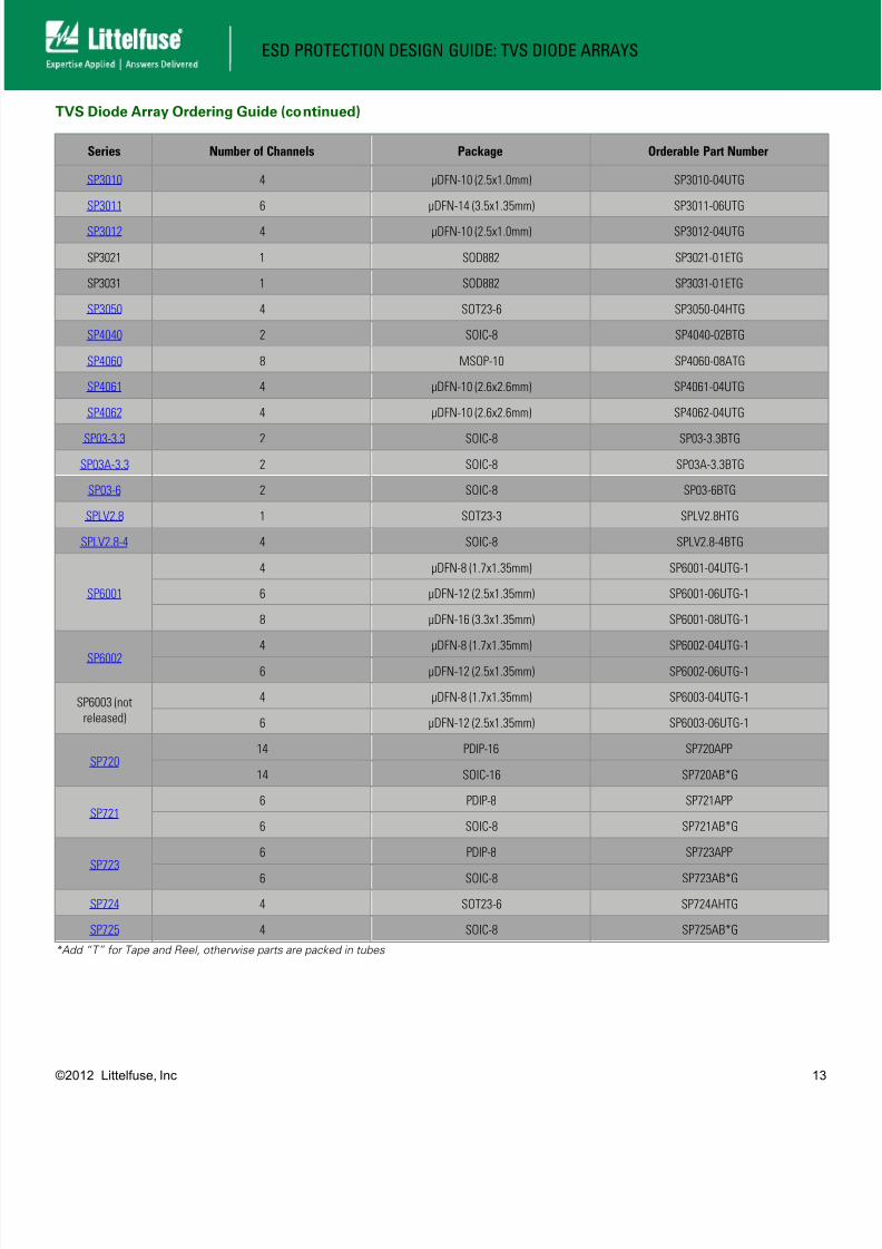
TVS Diode Array Ordering Guide (continued)
Series Number of Channels Package Orderable Part Number
SP3010 4 μDFN-10 (2.5x1.0mm) SP3010-04UTG
SP3011 6 μDFN-14 (3.5x1.35mm) SP3011-06UTG
SP3012 4 μDFN-10 (2.5x1.0mm) SP3012-04UTG
SP3021 1 SOD882 SP3021-01ETG
SP3031 1 SOD882 SP3031-01ETG
SP3050 4 SOT23-6 SP3050-04HTG
SP4040 2 SOIC-8 SP4040-02BTG
SP4060 8 MSOP-10 SP4060-08ATG
SP4061 4 μDFN-10 (2.6x2.6mm) SP4061-04UTG
SP4062 4 μDFN-10 (2.6x2.6mm) SP4062-04UTG
SP03-3.3 2 SOIC-8 SP03-3.3BTG
SP03A-3.3 2 SOIC-8 SP03A-3.3BTG
SP03-6 2 SOIC-8 SP03-6BTG
SPLV2.8 1 SOT23-3 SPLV2.8HTG
SPLV2.8-4 4 SOIC-8 SPLV2.8-4BTG
SP6001
4 μDFN-8 (1.7x1.35mm) SP6001-04UTG-1
6 μDFN-12 (2.5x1.35mm) SP6001-06UTG-1
8 μDFN-16 (3.3x1.35mm) SP6001-08UTG-1
SP6002
4 μDFN-8 (1.7x1.35mm) SP6002-04UTG-1
6 μDFN-12 (2.5x1.35mm) SP6002-06UTG-1
SP6003 (not
released)
4 μDFN-8 (1.7x1.35mm) SP6003-04UTG-1
6 μDFN-12 (2.5x1.35mm) SP6003-06UTG-1
SP720 14 PDIP-16 SP720APP
14 SOIC-16 SP720AB*G
SP721 6 PDIP-8 SP721APP
6 SOIC-8 SP721AB*G
SP723 6 PDIP-8 SP723APP
6 SOIC-8 SP723AB*G
SP724 4 SOT23-6 SP724AHTG
SP725 4 SOIC-8 SP725AB*G
*Add “T” for Tape and Reel, otherwise parts are packed in tubes
8/10/2019 Littelfuse Esd Protection Design Guide.pdf
http://slidepdf.com/reader/full/littelfuse-esd-protection-design-guidepdf 14/47
ESD PROTECTION DESIGN GUIDE: TVS DIODE ARRAYS
©2012 Littelfuse, Inc 14
Application Specific Device SelectionUSB1.1
Considerations:
● Each port operates at either 1.5Mbps or 12Mbps (low and full speed respectively)
• Parasitic capacitance should be taken into account although these relatively slow speeds can tolerate tens of picofarads
● Requires 2 channels of data line protection per port (i.e. D±)
• A 4 channel device can be useful if protecting a USB stack of 2 ports to make the ESD footprint as small as possible
• VBUS can be protected separately with a single channel device in an 0402 or 0201 form factor (0402 shown)
Application Schematic:
Recommended SPA Devices:
Ordering NumberESD Level
(Contact)I/O Capacitance @ VR=2.5V # of Channels VRWM Packaging
SP0502BAJTG ±30kV 30pF 2 5.5V SC70-3
SP1001-02XTG ±15kV 8pF 2 5.5V SOT553
SP1003-01ETG ±30kV 17pF 1 5.0V 0402 (SOD882)
SP1003-01DTG ±30kV 17pF 1 5.0V 0402 (SOD723)
SP1006-01UTG ±30kV 15pF 1 5.0V 0201 (µDFN-2)
Signal GNDCase GND
USB ControllerUSB Port
SP0502Outside
World
Case GND
SP1003
VBUS
D+
D-
IC
VBUS
D+
D-

8/10/2019 Littelfuse Esd Protection Design Guide.pdf
http://slidepdf.com/reader/full/littelfuse-esd-protection-design-guidepdf 15/47
ESD PROTECTION DESIGN GUIDE: TVS DIODE ARRAYS
©2012 Littelfuse, Inc 15
Application Specific Device SelectionUSB2.0
Considerations:
● Each port can operate up to 480Mbps
• The high data rate requires a low capacitance device to preserve signal integrity
● Requires 2 channels of data line protection per port (i.e. D±) which can be done via array or discretely
• A 4 channel device such as the SP3002-04 can be useful if protecting a USB stack of 2 ports to make the ESD footprint as small as possible
• VBUS can be protected by connecting it to the VCC pin on the diode array or by using a separate single channel device like the SP1003
Application Schematic:
Recommended SPA Devices:
Ordering NumberESD Level
(Contact)
I/O Capacitance @
VR=1.65V # of Channels VRWM Packaging
SP3003-02XTG ±8kV 0.65pF 2 6V SOT553
SP3003-02JTG ±8kV 0.65pF 2 6V SC70-5
SP3031-01ETG (2012 release) ±10kV 0.80pF 1 5V SOD882
Signal GNDCase GND
SP3003
OutsideWorld
Optional
VBUS
D+
D-
IC
NC
Signal GNDCase GND
USB Port
SP3031 (x2)
Outside
World
VBUS
D
D-
IC
USB Controller
*Package is shown as transparent
USB ControllerUSB Port
8/10/2019 Littelfuse Esd Protection Design Guide.pdf
http://slidepdf.com/reader/full/littelfuse-esd-protection-design-guidepdf 16/47
ESD PROTECTION DESIGN GUIDE: TVS DIODE ARRAYS
©2012 Littelfuse, Inc 16
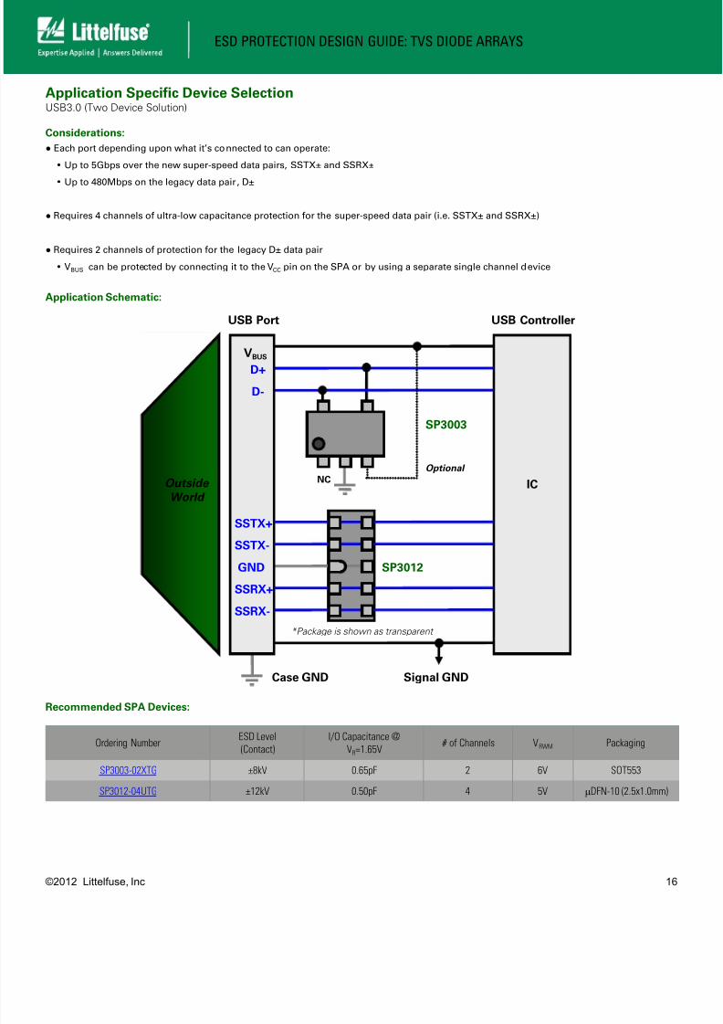
Application Specific Device SelectionUSB3.0 (Two Device Solution)
Considerations:
● Each port depending upon what it’s connected to can operate:
• Up to 5Gbps over the new super-speed data pairs, SSTX± and SSRX±
• Up to 480Mbps on the legacy data pair, D±
● Requires 4 channels of ultra-low capacitance protection for the super-speed data pair (i.e. SSTX± and SSRX±)
● Requires 2 channels of protection for the legacy D± data pair
• VBUS can be protected by connecting it to the VCC pin on the SPA or by using a separate single channel device
Application Schematic:
Recommended SPA Devices:
Ordering NumberESD Level
(Contact)
I/O Capacitance @
VR=1.65V # of Channels VRWM Packaging
SP3003-02XTG ±8kV 0.65pF 2 6V SOT553
SP3012-04UTG ±12kV 0.50pF 4 5V μDFN-10 (2.5x1.0mm)
Signal GNDCase GND
USB ControllerUSB Port
SP3003
Outside
World
Optional
SSTX+
SSTX-
SSRX+
SSRX-
GND
D+
D-
SP3012
ICNC
*Package is shown as transparent
VBUS

8/10/2019 Littelfuse Esd Protection Design Guide.pdf
http://slidepdf.com/reader/full/littelfuse-esd-protection-design-guidepdf 17/47
ESD PROTECTION DESIGN GUIDE: TVS DIODE ARRAYS
©2012 Littelfuse, Inc 17
Application Specific Device SelectionUSB3.0 (Fully Integrated Solution)
Considerations:
● Each port depending upon what it’s connected to can operate:
• Up to 5Gbps over the new super-speed data pairs, SSTX± and SSRX±
• Up to 480Mbps on the legacy data pair, D±
● Requires 4 channels of ultra-low capacitance protection for the super-speed data pair (i.e. SSTX± and SSRX±) and 2 channels of protection
for the legacy D± data pair. The SP3011 shown below integrates all 6 channels of protection into a small form factor µDFN-14 package.
Application Schematic:
Recommended SPA Devices:
Ordering NumberESD Level
(Contact)I/O Capacitance @ VR=0V # of Channels VRWM Packaging
SP3011-06UTG ±8kV 0.40pF 6 6V μDFN-14 (3.5x1.35mm)
Signal GNDCase GND
USB ControllerUSB Port
Outside
World
SSTX+
SSTX-
SSRX+
SSRX-
GND
D+
D-
SP3011
IC
* Package is shown as transparent
VBUS

8/10/2019 Littelfuse Esd Protection Design Guide.pdf
http://slidepdf.com/reader/full/littelfuse-esd-protection-design-guidepdf 18/47
ESD PROTECTION DESIGN GUIDE: TVS DIODE ARRAYS
©2012 Littelfuse, Inc 18
Application Specific Device SelectionHDMI
Considerations:
● Each port has 3 differential pairs of data (i.e. D0±, D1±, D2±) plus a clock (CLK±)
• For HDMI 1.1-1.2 the throughput is a total of 4.95Gbps (1.65Gbps per lane)
• For HDMI 1.3-1.4 the throughput is a total of 10.2Gbps (3.4Gbps per lane)
● To maintain the differential impedance per the HDMI Compliance Test Specification (and consequently signal integrity) a very lowcapacitance device must be used
● To maintain the differential impedance the designer should avoid using 90º angles and vias
• This can be accomplished by the use of an ESD device that offers a “straight-through” routing scheme
● Requires 12 channels of protection : 8 TMDS data pairs, SDA, SCL, CEC, and HPD
Application Schematic:
Recommended SPA Devices:
Ordering NumberESD Level
(Contact)
I/O Capacitance @
VR=1.65V # of Channels VRWM Packaging
SP3010-04UTG ±8kV 0.45pF 4 6V μDFN-10 (2.5x1.0mm)
SP3012-04UTG) ±12kV 0.50pF 4 5V μDFN-10 (2.5x1.0mm)
D2+
Case GND
OutsideWorld
GND
D2-
D1+
GND
D1-
D0+
GND
D0-
CLK+
GND
CLK-
SP3010
SP3010
*Package is shown as transparent
SignalGND
SDA
SCL
CEC
HPD
IC
SP3010
ChipsetHDMI Port

8/10/2019 Littelfuse Esd Protection Design Guide.pdf
http://slidepdf.com/reader/full/littelfuse-esd-protection-design-guidepdf 19/47
ESD PROTECTION DESIGN GUIDE: TVS DIODE ARRAYS
©2012 Littelfuse, Inc 19
Application Specific Device SelectionHDMI (includes protection for Ethernet and 5V power)
Considerations:
● Same as noted on previous page except the protection scheme below includes options for protecting additional Ethernet and 5V power pins.
● Other combinations exist such as using 2, 6 channel SP3011 devices along with 2, single channel discrete
Application Schematic:
Recommended SPA Devices:
Ordering Number ESD Level (Contact) I/O Capacitance @ VR=2.5V # of Channels VRWM Packaging
SP3010-04UTG ±8kV 0.45pF 4 6V μDFN-10 (2.5x1.0mm)
SP3012-04UTG) ±12kV 0.50pF 4 5V μDFN-10 (2.5x1.0mm)
SP3021-01ETG (2012 release) ±8kV 0.50pF 1 5V 0402 (SOD882)
SP1003-01ETG (SP1003) ±30kV 17pF 1 6V 0402 (SOD882)
D2+
Case GND
Outside
World
GND
D2-
D1+
GND
D1-
D0+
GND
D0-
CLK+
GND
CLK-
SP3010
SP3010
*Package is shown as transparent
Signal GND
SDA
SCL
CEC
HPD
IC
SP3010
PWR
ENET
SP3021
SP1003
HDMI Port Chipset
8/10/2019 Littelfuse Esd Protection Design Guide.pdf
http://slidepdf.com/reader/full/littelfuse-esd-protection-design-guidepdf 20/47
ESD PROTECTION DESIGN GUIDE: TVS DIODE ARRAYS
©2012 Littelfuse, Inc 20
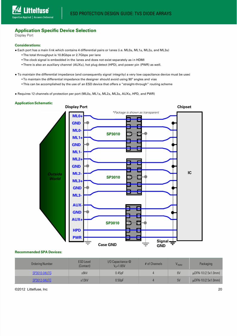
Application Specific Device SelectionDisplay Port
Considerations:
● Each port has a main link which contains 4 differential pairs or lanes (i.e. ML0±, ML1±, ML2±, and ML3±)
• The total throughput is 10.8Gbps or 2.7Gbps per lane
• The clock signal is embedded in the lanes and does not exist separately as in HDMI
• There is also an auxiliary channel (AUX±), hot plug detect (HPD), and power pin (PWR) as well.
● To maintain the differential impedance (and consequently signal integrity) a very low capacitance device must be used
• To maintain the differential impedance the designer should avoid using 90º angles and vias
• This can be accomplished by the use of an ESD device that offers a “straight-through” routing scheme
● Requires 12 channels of protection per port (ML0±, ML1±, ML2±, ML3±, AUX±, HPD, and PWR)
Application Schematic:
Recommended SPA Devices:
Ordering NumberESD Level
(Contact)
I/O Capacitance @
VR=1.65V # of Channels VRWM Packaging
SP3010-04UTG ±8kV 0.45pF 4 6V μDFN-10 (2.5x1.0mm)
SP3012-04UTG ±12kV 0.50pF 4 5V μDFN-10 (2.5x1.0mm)
ML0+
Case GND
Outside
World
GND
ML0-
ML1+
GND
ML1-
ML2+
GND
ML2-
ML3+
GND
ML3-
SP3010
SP3010
*Package is shown as transparent
Signal
GND
AUX-
AUX+
GND
HPD
PWR
IC
SP3010
ChipsetDisplay Port
8/10/2019 Littelfuse Esd Protection Design Guide.pdf
http://slidepdf.com/reader/full/littelfuse-esd-protection-design-guidepdf 21/47
ESD PROTECTION DESIGN GUIDE: TVS DIODE ARRAYS
©2012 Littelfuse, Inc 21
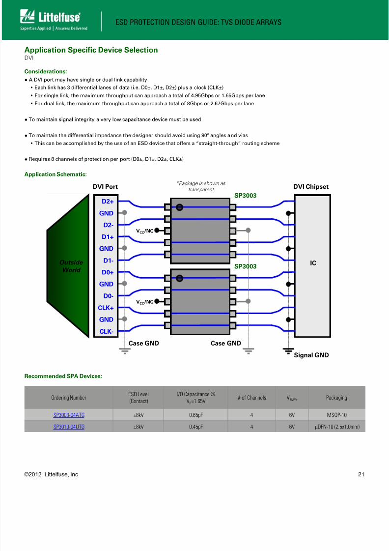
Application Specific Device SelectionDVI
Considerations:
● A DVI port may have single or dual link capability
• Each link has 3 differential lanes of data (i.e. D0±, D1±, D2±) plus a clock (CLK±)
• For single link, the maximum throughput can approach a total of 4.95Gbps or 1.65Gbps per lane• For dual link, the maximum throughput can approach a total of 8Gbps or 2.67Gbps per lane
● To maintain signal integrity a very low capacitance device must be used
● To maintain the differential impedance the designer should avoid using 90º angles and vias
• This can be accomplished by the use of an ESD device that offers a “straight-through” routing scheme
● Requires 8 channels of protection per port (D0±, D1±, D2±, CLK±)
Application Schematic:
Recommended SPA Devices:
Ordering NumberESD Level
(Contact)
I/O Capacitance @
VR=1.65V # of Channels VRWM Packaging
SP3003-04ATG ±8kV 0.65pF 4 6V MSOP-10
SP3010-04UTG ±8kV 0.45pF 4 6V μDFN-10 (2.5x1.0mm)
D2+
Case GND
DVI ChipsetDVI Port
Outside
World
GND
D2-
D1+
GND
D1-
D0+
GND
D0-
CLK+
GND
CLK-
Case GND
VCC/NC
VCC/NC
*Package is shown as
transparent
IC
Signal GND
SP3003
SP3003

8/10/2019 Littelfuse Esd Protection Design Guide.pdf
http://slidepdf.com/reader/full/littelfuse-esd-protection-design-guidepdf 22/47
ESD PROTECTION DESIGN GUIDE: TVS DIODE ARRAYS
©2012 Littelfuse, Inc 22
Application Specific Device Selection10/100/1000 Ethernet, Intra-building Lightning Immunity (GR-1089)
Considerations:
● 10/100/1000 relates to the data rate in Mbps (i.e. 10Mbps, 100Mbps, and 1000Mbps)
• For 10 Base-T, data is transmitted over 2 UTP (unshielded twisted pairs) using a 10MHz clock
• For 100 Base-TX, data is transmitted over 2 UTP using a 125MHz clock• For 1000 Base-T data is transmitted over 4 UTP using a 125MHz clock
• For these data rates the parasitic capacitance needs to be taken into account to preserve signal integrity
● The 4 data lines below (Tx± and Rx±) are being protected against intra-building (i.e. 100A, tP=2/10µs) lightning transients by a two-stageprotection scheme
● 1000Mbps Ethernet (or 1GbE) will require 8 channels of protection for the 4 differential pair so the below scheme should be replicated for theremaining 2 data pair
Application Schematic:
Recommended SPA Devices:
Ordering NumberESD Level
(Contact)
Lightning
(tP=8/20μs)
I/O Capacitance @
VR=0V # of Channels VRWM Packaging
SP03A-xBTG ±30kV 150A 4.5pF (I/O to I/O) 2 3.3V SOIC-8
SP03-3.3BTG ±30kV 150A 8pF (I/O to I/O) 2 3.3V,6V SOIC-8
SP3050-04HTG ±20kV 10A 2.4pF 4 6V SOT23-6
Ethernet PH
Outside
World
Tx-
Rx+
Rx-
J1
J8
SP03A (x2)
Tx+
RJ-45Connector
PHY GND SP3050
F1:F4 = 0461 1.25 TeleLink Fuse
F1
F2
F3
F4

8/10/2019 Littelfuse Esd Protection Design Guide.pdf
http://slidepdf.com/reader/full/littelfuse-esd-protection-design-guidepdf 23/47
ESD PROTECTION DESIGN GUIDE: TVS DIODE ARRAYS
©2012 Littelfuse, Inc 23
Application Specific Device Selection10/100/1000 Ethernet, Inter-building Lightning Immunity (GR-1089)
Considerations:
● 10/100/1000 relates to the data rate in Mbps (i.e. 10Mbps, 100Mbps, and 1000Mbps)
• For 10 Base-T, data is transmitted over 2 UTP (unshielded twisted pairs) using a 10MHz clock
• For 100 Base-TX, data is transmitted over 2 UTP using a 125MHz clock• For 1000 Base-T data is transmitted over 4 UTP using a 125MHz clock
• For these data rates the parasitic capacitance needs to be taken into account to preserve signal integrity
● The 4 data lines below are being protected against inter-building (i.e. 500A, tP=2/10µs) lightning transients by a two-stage protection scheme.The 4 channel, SP4061 or SP4062 should be selected based on the operating voltage of the PHY.
● The standoff voltage of the SEP Series device will be dictated by the use of PoE. If PoE is present the SEP0640 should be used; otherwise,the SEP0080 is ok for non-PoE applications. Note: Higher voltage options are available for atypical PoE voltages.
● 1000Mbps Ethernet (or 1GbE) will require 8 channels of protection for the 4 differential pair so the below scheme should be replicated for theremaining 2 data pair
Application Schematic:
Recommended SPA Devices:
Ordering NumberESD Level
(Contact)
Lightning
(tP=8/20μs)
I/O Capacitance @
VR=0V # of Channels VRWM Packaging
SEP0080Q38CB ±30kV 400A See datasheet 2 6V QFN
SEP0640Q38CB ±30kV 400A See datasheet 2 58V QFN
SP4061-04UTG ±30kV 20A 3.5pF 4 2.5V µDFN-10 (2.6x2.6mm)
SP4062-04UTG ±30kV 20A 3.5pF 4 3.3V µDFN-10 (2.6x2.6mm)
Ethernet PH
Outside
World
Case GND
Tx-
Rx+
Rx-
J1
J8
SEP0xx (x2)
Tx+
PHY
GND
SP4062
F1:F4 = 0461 1.25 TeleLink Fuse
F1
F2
F3
F4
*Package is shown as transparentRJ-45Connector
8/10/2019 Littelfuse Esd Protection Design Guide.pdf
http://slidepdf.com/reader/full/littelfuse-esd-protection-design-guidepdf 24/47
ESD PROTECTION DESIGN GUIDE: TVS DIODE ARRAYS
©2012 Littelfuse, Inc 24
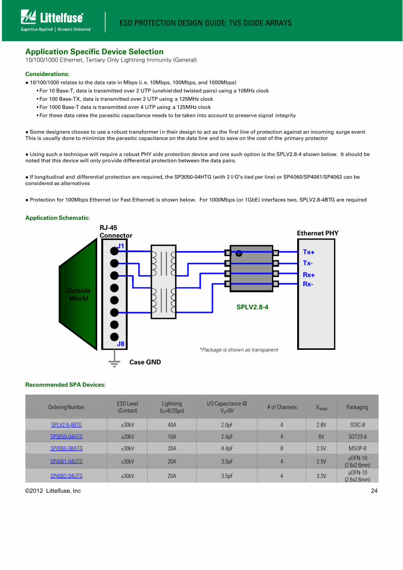
Application Specific Device Selection10/100/1000 Ethernet, Tertiary Only Lightning Immunity (General)
Considerations:
● 10/100/1000 relates to the data rate in Mbps (i.e. 10Mbps, 100Mbps, and 1000Mbps)
• For 10 Base-T, data is transmitted over 2 UTP (unshielded twisted pairs) using a 10MHz clock
• For 100 Base-TX, data is transmitted over 2 UTP using a 125MHz clock• For 1000 Base-T data is transmitted over 4 UTP using a 125MHz clock
• For these data rates the parasitic capacitance needs to be taken into account to preserve signal integrity
● Some designers choose to use a robust transformer in their design to act as the first line of protection against an incoming surge event.This is usually done to minimize the parasitic capacitance on the data line and to save on the cost of the primary protector
● Using such a technique will require a robust PHY side protection device and one such option is the SPLV2.8-4 shown below. It should benoted that this device will only provide differential protection between the data pairs.
● If longitudinal and differential protection are required, the SP3050-04HTG (with 2 I/O’s tied per line) or SP4060/SP4061/SP4062 can beconsidered as alternatives
● Protection for 100Mbps Ethernet (or Fast Ethernet) is shown below. For 1000Mbps (or 1GbE) interfaces two, SPLV2.8-4BTG are required
Application Schematic:
Recommended SPA Devices:
Ordering NumberESD Level
(Contact)
Lightning
(tP=8/20μs)
I/O Capacitance @
VR=0V # of Channels VRWM Packaging
SPLV2.8-4BTG ±30kV 40A 2.0pF 4 2.8V SOIC-8
SP3050-04HTG ±20kV 10A 2.4pF 4 6V SOT23-6
SP4060-08ATG ±30kV 20A 4.4pF 8 2.5V MSOP-8
SP4061-04UTG ±30kV 20A 3.5pF 4 2.5VµDFN-10
(2.6x2.6mm)
SP4062-04UTG ±30kV 20A 3.5pF 4 3.3VµDFN-10
(2.6x2.6mm)
Case GND
Outside
World
RJ-45Connector
J1
J8
SPLV2.8-4
EthernetPHY
Ethernet PHY
Tx+
Tx-
Rx+
Rx-
*Package is shown as transparent
8/10/2019 Littelfuse Esd Protection Design Guide.pdf
http://slidepdf.com/reader/full/littelfuse-esd-protection-design-guidepdf 25/47
ESD PROTECTION DESIGN GUIDE: TVS DIODE ARRAYS
©2012 Littelfuse, Inc 25
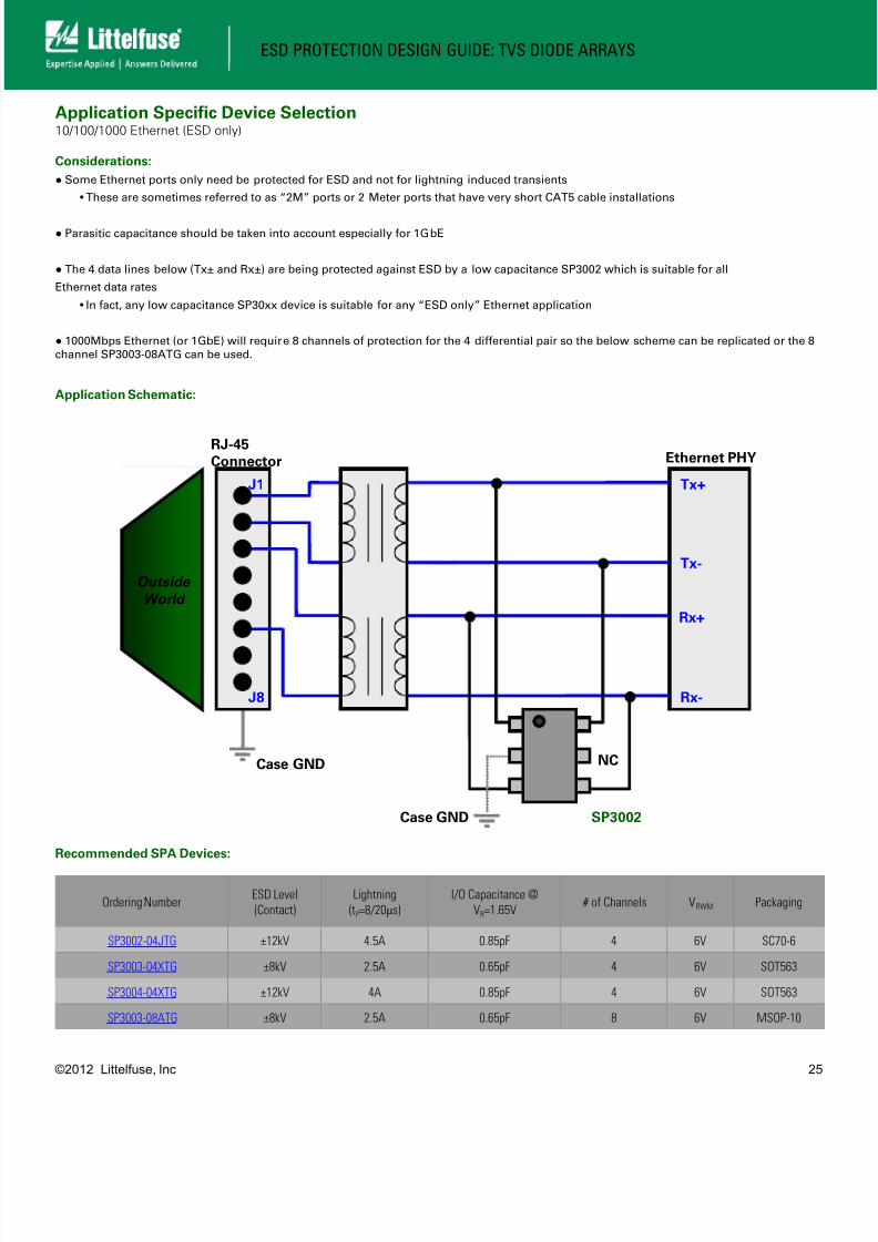
Application Specific Device Selection10/100/1000 Ethernet (ESD only)
Considerations:
● Some Ethernet ports only need be protected for ESD and not for lightning induced transients
• These are sometimes referred to as “2M” ports or 2 Meter ports that have very short CAT5 cable installations
● Parasitic capacitance should be taken into account especially for 1GbE
● The 4 data lines below (Tx± and Rx±) are being protected against ESD by a low capacitance SP3002 which is suitable for all
Ethernet data rates
• In fact, any low capacitance SP30xx device is suitable for any “ESD only” Ethernet application
● 1000Mbps Ethernet (or 1GbE) will require 8 channels of protection for the 4 differential pair so the below scheme can be replicated or the 8channel SP3003-08ATG can be used.
Application Schematic:
Recommended SPA Devices:
Ordering NumberESD Level
(Contact)
Lightning
(tP=8/20μs)
I/O Capacitance @
VR=1.65V # of Channels VRWM Packaging
SP3002-04JTG ±12kV 4.5A 0.85pF 4 6V SC70-6
SP3003-04XTG ±8kV 2.5A 0.65pF 4 6V SOT563
SP3004-04XTG ±12kV 4A 0.85pF 4 6V SOT563
SP3003-08ATG ±8kV 2.5A 0.65pF 8 6V MSOP-10
RJ-45Connector Ethernet PHY
Outside
World
Case GND
J1
J8
Case GND SP3002
NC
Tx-
Rx+
Rx-
Tx+
8/10/2019 Littelfuse Esd Protection Design Guide.pdf
http://slidepdf.com/reader/full/littelfuse-esd-protection-design-guidepdf 26/47
ESD PROTECTION DESIGN GUIDE: TVS DIODE ARRAYS
©2012 Littelfuse, Inc 26
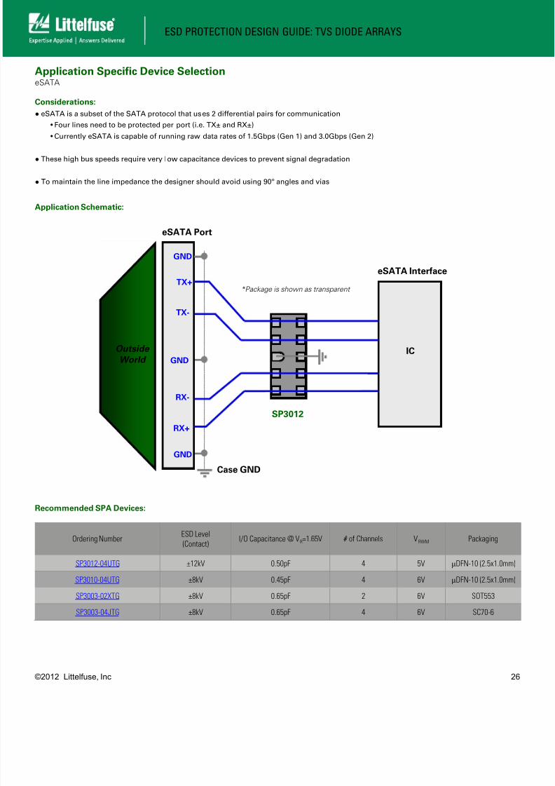
Application Specific Device SelectioneSATA
Considerations:
● eSATA is a subset of the SATA protocol that uses 2 differential pairs for communication
• Four lines need to be protected per port (i.e. TX± and RX±)
• Currently eSATA is capable of running raw data rates of 1.5Gbps (Gen 1) and 3.0Gbps (Gen 2)
● These high bus speeds require very low capacitance devices to prevent signal degradation
● To maintain the line impedance the designer should avoid using 90º angles and vias
Application Schematic:
Recommended SPA Devices:
Ordering NumberESD Level
(Contact)I/O Capacitance @ VR=1.65V # of Channels VRWM Packaging
SP3012-04UTG ±12kV 0.50pF 4 5V μDFN-10 (2.5x1.0mm)
SP3010-04UTG ±8kV 0.45pF 4 6V μDFN-10 (2.5x1.0mm)
SP3003-02XTG ±8kV 0.65pF 2 6V SOT553
SP3003-04JTG ±8kV 0.65pF 4 6V SC70-6
GND
Case GND
eSATA Interface
eSATA Port
Outside
World
TX+
TX-
GND
RX-
RX+
GND
*Package is shown as transparent
IC
SP3012
8/10/2019 Littelfuse Esd Protection Design Guide.pdf
http://slidepdf.com/reader/full/littelfuse-esd-protection-design-guidepdf 27/47
ESD PROTECTION DESIGN GUIDE: TVS DIODE ARRAYS
©2012 Littelfuse, Inc 27
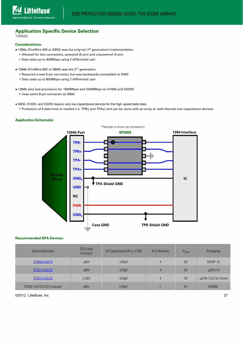
Application Specific Device Selection1394a/b
Considerations:
● 1394a (FireWire 400 or S400) was the original (1st generation) implementation
• Allowed for two connectors, powered (6 pin) and unpowered (4 pin)
• Data rates up to 400Mbps using 2 differential pair
● 1394b (FireWire 800 or S800) was the 2nd generation
• Required a new 9 pin connector but was backwards compatible to S400
• Data rates up to 800Mbps using 2 differential pair
● 1394b also had provisions for 1600Mbps and 3200Mbps (or S1600 and S3200)
• Uses same 9 pin connector as S800
● S800, S1600, and S3200 require very low capacitance devices for the high speed data rates
• Protection of 4 data lines is needed (i.e. TPB± and TPA±) and can be done with an array or with discrete low capacitance devices
Application Schematic:
Recommended SPA Devices:
Ordering NumberESD Level
(Contact)I/O Capacitance @ VR=1.65V # of Channels VRWM Packaging
SP3003-04ATG ±8kV 0.65pF 4 6V MSOP-10
SP3010-04UTG ±8kV 0.45pF 4 6V μDFN-10
SP3012-04UTG ±12kV 0.50pF 4 5V μDFN-10 (2.5x1.0mm
SP3021-01ETG (2012 release) ±8kV 0.50pF 1 5V SOD882
Case GND
1394 Interface1394b Port
Outside
World
TPB-
TPB+
GNDS
PWR
GNDS
TPA-
TPA+
GND
NC
TPA Shield GND
TPB Shield GND
IC
SP3003
*Package is shown as transparent

8/10/2019 Littelfuse Esd Protection Design Guide.pdf
http://slidepdf.com/reader/full/littelfuse-esd-protection-design-guidepdf 28/47
ESD PROTECTION DESIGN GUIDE: TVS DIODE ARRAYS
©2012 Littelfuse, Inc 28
Application Specific Device SelectionLVDS (Low Voltage Differential Signaling)
Considerations:
● LVDS is a low noise, low-voltage signal scheme that uses a small current (typically 3.5mA) to generate a voltage drop across a 100Ω resistor
to convey information or data
• Data rates can vary per application but the ANSI/TIA/EIA-644-A standard recommends a maximum of 655Mbps
● The medium/high speed bus requires a low capacitance device in 1-6pF range (typically)
• LVDS schemes will vary in terms of the total number of channels used
• Protection of 8 data lines is shown below (i.e. CLK± and Ax±)
Application Schematic:
Recommended SPA Devices:
Ordering NumberESD Level
(Contact)
Lightning
(tP=8/20μs)I/O Capacitance @ VR=0V # of Channels VRWM Packaging
SP4060-08ATG ±30kV 20A 4.4pF 8 2.5V MSOP-10
SP3050-04HTG ±20kV 10A 2.4pF 4 6V SOT23-6
SP4061-04UTG ±30kV 20A 3.5pF 4 2.5V µDFN-10 (2.6x2.6mm)
Outside
World
CLK+
Case GND
LVDS Interface
CLK-
A0+
A0-
A1+
A1-
A2+
A2-
Signal GND
Case GND
SP4060
IC
LVDS Controller
8/10/2019 Littelfuse Esd Protection Design Guide.pdf
http://slidepdf.com/reader/full/littelfuse-esd-protection-design-guidepdf 29/47
ESD PROTECTION DESIGN GUIDE: TVS DIODE ARRAYS
©2012 Littelfuse, Inc 29
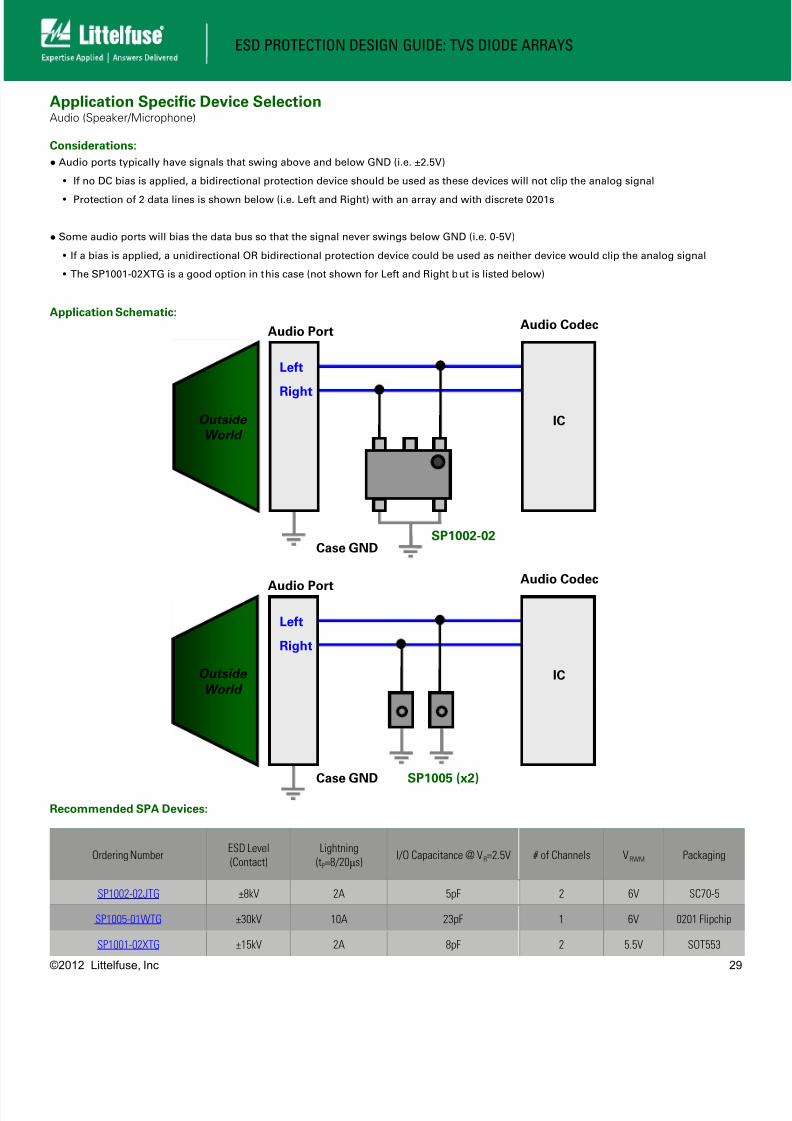
Application Specific Device SelectionAudio (Speaker/Microphone)
Considerations:
● Audio ports typically have signals that swing above and below GND (i.e. ±2.5V)
• If no DC bias is applied, a bidirectional protection device should be used as these devices will not clip the analog signal
• Protection of 2 data lines is shown below (i.e. Left and Right) with an array and with discrete 0201s
● Some audio ports will bias the data bus so that the signal never swings below GND (i.e. 0-5V)
• If a bias is applied, a unidirectional OR bidirectional protection device could be used as neither device would clip the analog signal
• The SP1001-02XTG is a good option in this case (not shown for Left and Right but is listed below)
Application Schematic:
Recommended SPA Devices:
Ordering NumberESD Level
(Contact)
Lightning
(tP=8/20μs)I/O Capacitance @ VR=2.5V # of Channels VRWM Packaging
SP1002-02JTG ±8kV 2A 5pF 2 6V SC70-5
SP1005-01WTG ±30kV 10A 23pF 1 6V 0201 Flipchip
SP1001-02XTG ±15kV 2A 8pF 2 5.5V SOT553
Outside
World
Left
Audio Port
Right
IC
Case GND SP1005 (x2)
Outside
World
Left
Audio Port
Right
IC
Case GNDSP1002-02
Audio Codec
Audio Codec
8/10/2019 Littelfuse Esd Protection Design Guide.pdf
http://slidepdf.com/reader/full/littelfuse-esd-protection-design-guidepdf 30/47
ESD PROTECTION DESIGN GUIDE: TVS DIODE ARRAYS
©2012 Littelfuse, Inc 30
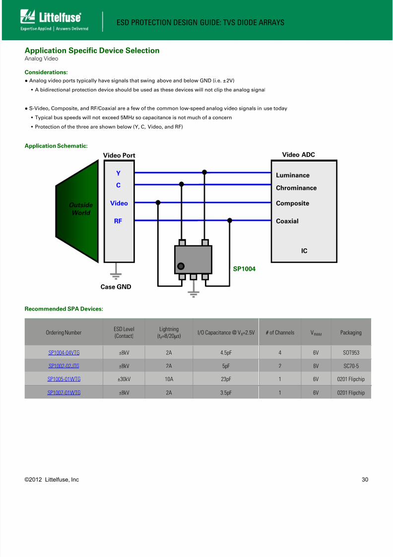
Application Specific Device SelectionAnalog Video
Considerations:
● Analog video ports typically have signals that swing above and below GND (i.e. ±2V)
• A bidirectional protection device should be used as these devices will not clip the analog signal
● S-Video, Composite, and RF/Coaxial are a few of the common low-speed analog video signals in use today
• Typical bus speeds will not exceed 5MHz so capacitance is not much of a concern
• Protection of the three are shown below (Y, C, Video, and RF)
Application Schematic:
Recommended SPA Devices:
Ordering NumberESD Level
(Contact)
Lightning
(tP=8/20μs)I/O Capacitance @ VR=2.5V # of Channels VRWM Packaging
SP1004-04VTG ±8kV 2A 4.5pF 4 6V SOT953
SP1002-02JTG ±8kV 2A 5pF 2 6V SC70-5
SP1005-01WTG ±30kV 10A 23pF 1 6V 0201 Flipchip
SP1007-01WTG ±8kV 2A 3.5pF 1 6V 0201 Flipchip
Outside
World
Y
Case GND
Video Port
C Chrominance
Luminance
Composite
IC
Video
RF Coaxial
SP1004
Video ADC
8/10/2019 Littelfuse Esd Protection Design Guide.pdf
http://slidepdf.com/reader/full/littelfuse-esd-protection-design-guidepdf 31/47
ESD PROTECTION DESIGN GUIDE: TVS DIODE ARRAYS
©2012 Littelfuse, Inc 31
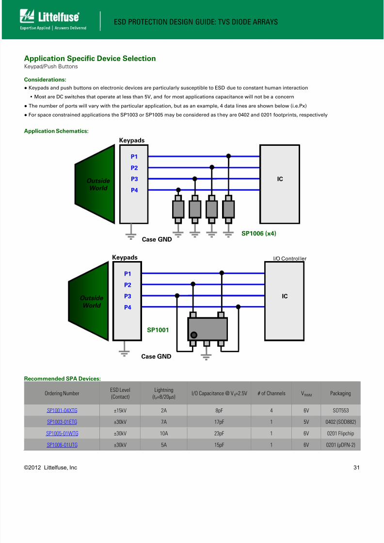
Application Specific Device SelectionKeypad/Push Buttons
Considerations:
● Keypads and push buttons on electronic devices are particularly susceptible to ESD due to constant human interaction
• Most are DC switches that operate at less than 5V, and for most applications capacitance will not be a concern
● The number of ports will vary with the particular application, but as an example, 4 data lines are shown below (i.e.Px)
● For space constrained applications the SP1003 or SP1005 may be considered as they are 0402 and 0201 footprints, respectively
Application Schematics:
Recommended SPA Devices:
Ordering NumberESD Level
(Contact)
Lightning
(tP=8/20μs)I/O Capacitance @ VR=2.5V # of Channels VRWM Packaging
SP1001-04XTG ±15kV 2A 8pF 4 6V SOT553
SP1003-01ETG ±30kV 7A 17pF 1 5V 0402 (SOD882)
SP1005-01WTG ±30kV 10A 23pF 1 6V 0201 Flipchip
SP1006-01UTG ±30kV 5A 15pF 1 6V 0201 (µDFN-2)
Outside
World
P1
Case GND
Keypads
P2
ICP3
P4
SP1001
I/O Control ler
Outside
World
P1
Case GND
Keypads
P2
ICP3
P4
SP1006 (x4)

8/10/2019 Littelfuse Esd Protection Design Guide.pdf
http://slidepdf.com/reader/full/littelfuse-esd-protection-design-guidepdf 32/47
ESD PROTECTION DESIGN GUIDE: TVS DIODE ARRAYS
©2012 Littelfuse, Inc 32
Application Specific Device SelectionSIM Socket
Considerations:
● The SIM (Subscriber Identification Module) card has 3 data lines that are low-speed and low-voltage
• Given the low speed of the signals, the capacitance will not be a concern
● The low-voltage signal lines are best protected by a device which has a low standoff voltage or VRWM
● Protection of the 3 data lines is shown below (i.e. CLK, DATA, and RESET)
Application Schematics:
Recommended SPA Devices:
Ordering NumberESD Level
(Contact)
Lightning
(tP=8/20μs)
I/O Capacitance @
VR=1.65V
# of
ChannelsVRWM Packaging
SP3002-04UTG ±12kV 4.5A 0.85pF 4 6V μDFN-6 (1.6x1.6mm)
SP1011-04UTG ±15kV 2A 7pF 4 6V μDFN-6 (1.25x1.0mm)
SP1005-01WTG ±30kV 10A 23pF 1 6V 0201 Flipchip
SP1006-01UTG ±30kV 5A 15pF 1 6V 0201 (µDFN-2)
Signal GND
VBUS
DATA
CLK
RESET
GND
SP3002
Outside
World
Case GND
IC
Case GND
SIM Socket SIM Controller
8/10/2019 Littelfuse Esd Protection Design Guide.pdf
http://slidepdf.com/reader/full/littelfuse-esd-protection-design-guidepdf 33/47
ESD PROTECTION DESIGN GUIDE: TVS DIODE ARRAYS
©2012 Littelfuse, Inc 33
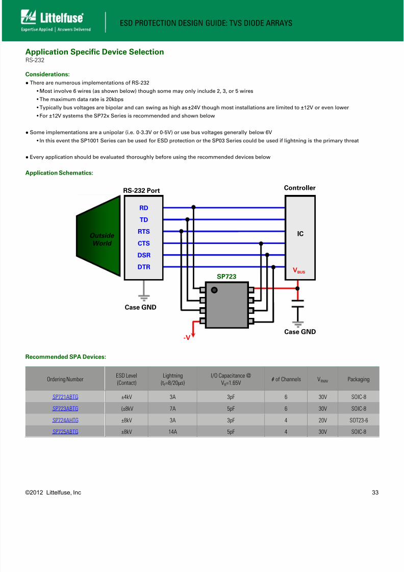
Application Specific Device SelectionRS-232
Considerations:
● There are numerous implementations of RS-232
• Most involve 6 wires (as shown below) though some may only include 2, 3, or 5 wires
• The maximum data rate is 20kbps• Typically bus voltages are bipolar and can swing as high as ±24V though most installations are limited to ±12V or even lower
• For ±12V systems the SP72x Series is recommended and shown below
● Some implementations are a unipolar (i.e. 0-3.3V or 0-5V) or use bus voltages generally below 6V
• In this event the SP1001 Series can be used for ESD protection or the SP03 Series could be used if lightning is the primary threat
● Every application should be evaluated thoroughly before using the recommended devices below
Application Schematics:
Recommended SPA Devices:
Ordering NumberESD Level
(Contact)
Lightning
(tP=8/20μs)
I/O Capacitance @
VR=1.65V # of Channels VRWM Packaging
SP721ABTG ±4kV 3A 3pF 6 30V SOIC-8
SP723ABTG (±8kV 7A 5pF 6 30V SOIC-8
SP724AHTG ±8kV 3A 3pF 4 20V SOT23-6
SP725ABTG ±8kV 14A 5pF 4 30V SOIC-8
RD
RS-232 Port
TD
SP723
ICRTS
CTS
Controller
DSR
DTR
Outside
World
Case GND
Case GND
VBUS
-V
8/10/2019 Littelfuse Esd Protection Design Guide.pdf
http://slidepdf.com/reader/full/littelfuse-esd-protection-design-guidepdf 34/47
ESD PROTECTION DESIGN GUIDE: TVS DIODE ARRAYS
©2012 Littelfuse, Inc 34
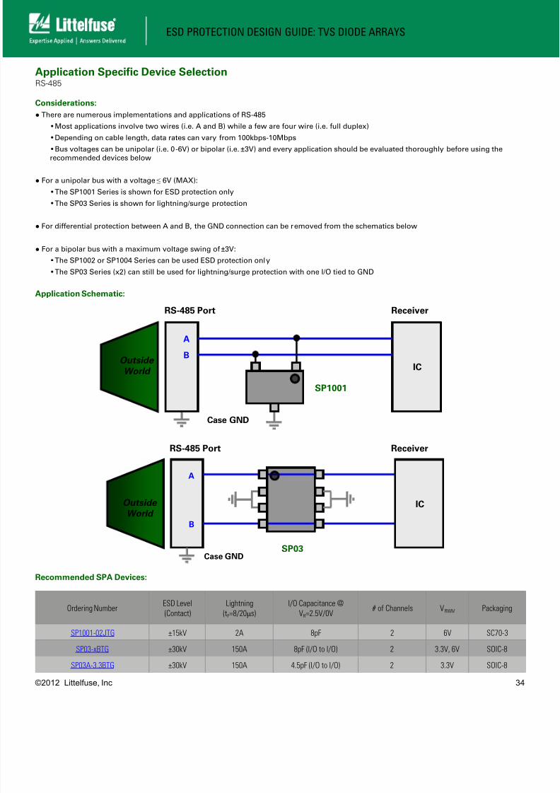
Application Specific Device SelectionRS-485
Considerations:
● There are numerous implementations and applications of RS-485
• Most applications involve two wires (i.e. A and B) while a few are four wire (i.e. full duplex)
• Depending on cable length, data rates can vary from 100kbps-10Mbps• Bus voltages can be unipolar (i.e. 0-6V) or bipolar (i.e. ±3V) and every application should be evaluated thoroughly before using therecommended devices below
● For a unipolar bus with a voltage ≤ 6V (MAX):
• The SP1001 Series is shown for ESD protection only
• The SP03 Series is shown for lightning/surge protection
● For differential protection between A and B, the GND connection can be removed from the schematics below
● For a bipolar bus with a maximum voltage swing of ±3V:
• The SP1002 or SP1004 Series can be used ESD protection only
• The SP03 Series (x2) can still be used for lightning/surge protection with one I/O tied to GND
Application Schematic:
Recommended SPA Devices:
Ordering NumberESD Level
(Contact)
Lightning
(tP=8/20μs)
I/O Capacitance @
VR=2.5V/0V # of Channels VRWM Packaging
SP1001-02JTG ±15kV 2A 8pF 2 6V SC70-3
SP03-xBTG ±30kV 150A 8pF (I/O to I/O) 2 3.3V, 6V SOIC-8
SP03A-3.3BTG ±30kV 150A 4.5pF (I/O to I/O) 2 3.3V SOIC-8
Receiver
Outside
World
A
RS-485 Port
B
IC
Case GND
SP03
Receiver
Outside
World
A
RS-485 Port
B
IC
Case GND
SP1001
8/10/2019 Littelfuse Esd Protection Design Guide.pdf
http://slidepdf.com/reader/full/littelfuse-esd-protection-design-guidepdf 35/47
ESD PROTECTION DESIGN GUIDE: TVS DIODE ARRAYS
©2012 Littelfuse, Inc 35
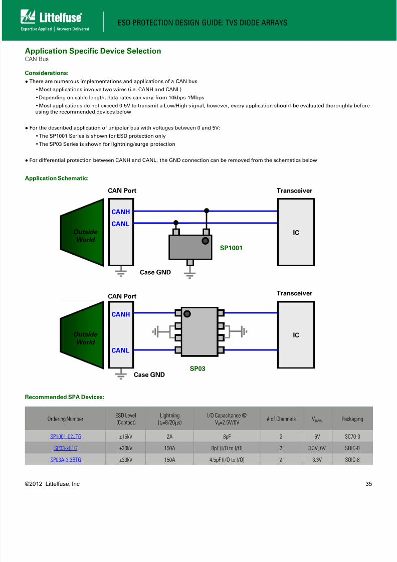
Application Specific Device SelectionCAN Bus
Considerations:
● There are numerous implementations and applications of a CAN bus
• Most applications involve two wires (i.e. CANH and CANL)
• Depending on cable length, data rates can vary from 10kbps-1Mbps• Most applications do not exceed 0-5V to transmit a Low/High signal, however, every application should be evaluated thoroughly beforeusing the recommended devices below
● For the described application of unipolar bus with voltages between 0 and 5V:
• The SP1001 Series is shown for ESD protection only
• The SP03 Series is shown for lightning/surge protection
● For differential protection between CANH and CANL, the GND connection can be removed from the schematics below
Application Schematic:
Recommended SPA Devices:
Ordering NumberESD Level
(Contact)
Lightning
(tP=8/20μs)
I/O Capacitance @
VR=2.5V/0V # of Channels VRWM Packaging
SP1001-02JTG ±15kV 2A 8pF 2 6V SC70-3
SP03-xBTG ±30kV 150A 8pF (I/O to I/O) 2 3.3V, 6V SOIC-8
SP03A-3.3BTG ±30kV 150A 4.5pF (I/O to I/O) 2 3.3V SOIC-8
Transceiver
Outside
World
CAN Port
IC
Case GNDSP03
CANH
CANL
Outside
World
CANH
CAN Port
CANL
IC
Case GND
SP1001
Transceiver
8/10/2019 Littelfuse Esd Protection Design Guide.pdf
http://slidepdf.com/reader/full/littelfuse-esd-protection-design-guidepdf 36/47
ESD PROTECTION DESIGN GUIDE: TVS DIODE ARRAYS
©2012 Littelfuse, Inc 36
Application Specific Device SelectionLCD and Camera Interfaces (Mobile)
Considerations:
● LCD and camera interfaces in mobile devices are vulnerable to EMI from the cellular band
• Frequencies between 800-3000MHz should be attenuated to prevent distortion on the display
● The pixel clocks vary depending upon the display size but the frequency will typically fall between 5-65MHz
• This corresponds to data rates between 10-60Mbps and with these speeds line capacitances need to be considered
• In the majority of applications line capacitances of 20-40pF will not cause signal integrity issues
● The protection schemes below for data lines Dx are only examples and will vary with the particular application
Application Schematic:
Recommended SPA Devices:
Ordering Number ESD Level(Contact)
Cut-off Frequency Line Capacitance@ VR=2.5V
# of Channels VRWM Packaging
SP6001-0xUTG-1 ±30kV 115MHz 24pF 4/6/8 6V μDFN-8/12/16
SP6002-0xUTG-1 ±30kV 100MHz 30pF 4/6 6V μDFN-8/12
SP6003-0xUTG-1 (not released yet) ±15kV 175MHz 14pF 4/6 6V μDFN-8/12
Baseband
D1
PCB Connector
for LCD Display
D2
SP6002-04
ICD3
D4
D1
Camera Module
D2
SP6001-06
ICD3
D4
Baseband
D5
D6
*Packages are shown as transparent
8/10/2019 Littelfuse Esd Protection Design Guide.pdf
http://slidepdf.com/reader/full/littelfuse-esd-protection-design-guidepdf 37/47
ESD PROTECTION DESIGN GUIDE: TVS DIODE ARRAYS
©2012 Littelfuse, Inc 37
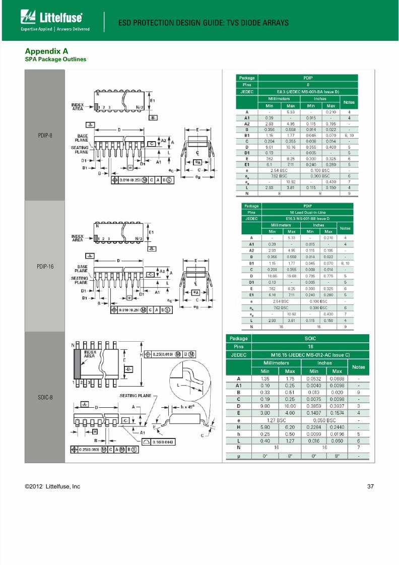
Appendix ASPA Package Outlines
PDIP-8
PDIP-16
SOIC-8
8/10/2019 Littelfuse Esd Protection Design Guide.pdf
http://slidepdf.com/reader/full/littelfuse-esd-protection-design-guidepdf 38/47
ESD PROTECTION DESIGN GUIDE: TVS DIODE ARRAYS
©2012 Littelfuse, Inc 38
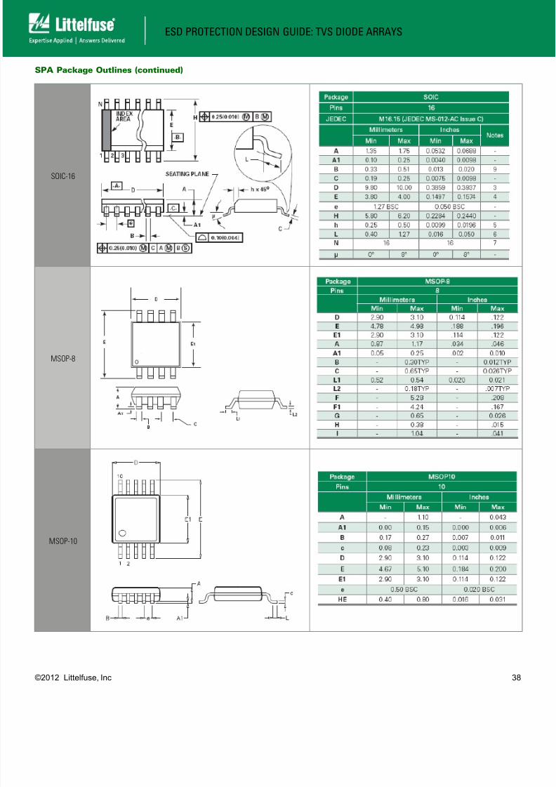
SPA Package Outlines (continued)
SOIC-16
MSOP-8
MSOP-10
8/10/2019 Littelfuse Esd Protection Design Guide.pdf
http://slidepdf.com/reader/full/littelfuse-esd-protection-design-guidepdf 39/47
ESD PROTECTION DESIGN GUIDE: TVS DIODE ARRAYS
©2012 Littelfuse, Inc 39
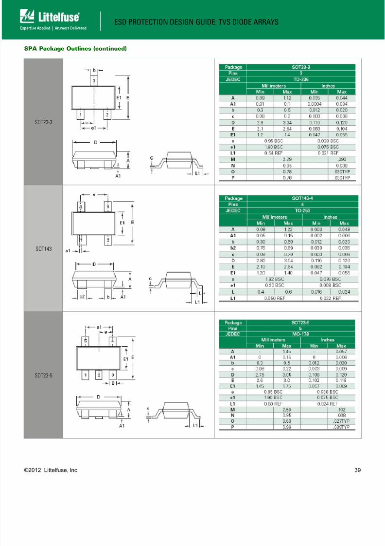
SPA Package Outlines (continued)
SOT23-3
SOT143
SOT23-5
8/10/2019 Littelfuse Esd Protection Design Guide.pdf
http://slidepdf.com/reader/full/littelfuse-esd-protection-design-guidepdf 40/47
ESD PROTECTION DESIGN GUIDE: TVS DIODE ARRAYS
©2012 Littelfuse, Inc 40
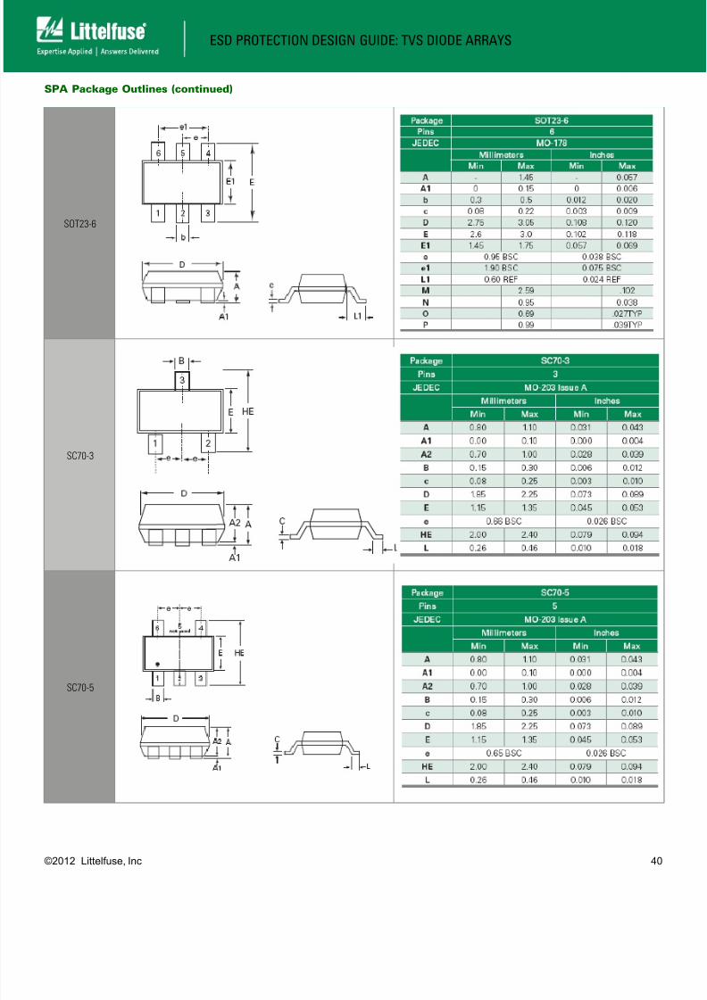
SPA Package Outlines (continued)
SOT23-6
SC70-3
SC70-5
8/10/2019 Littelfuse Esd Protection Design Guide.pdf
http://slidepdf.com/reader/full/littelfuse-esd-protection-design-guidepdf 41/47
ESD PROTECTION DESIGN GUIDE: TVS DIODE ARRAYS
©2012 Littelfuse, Inc 41
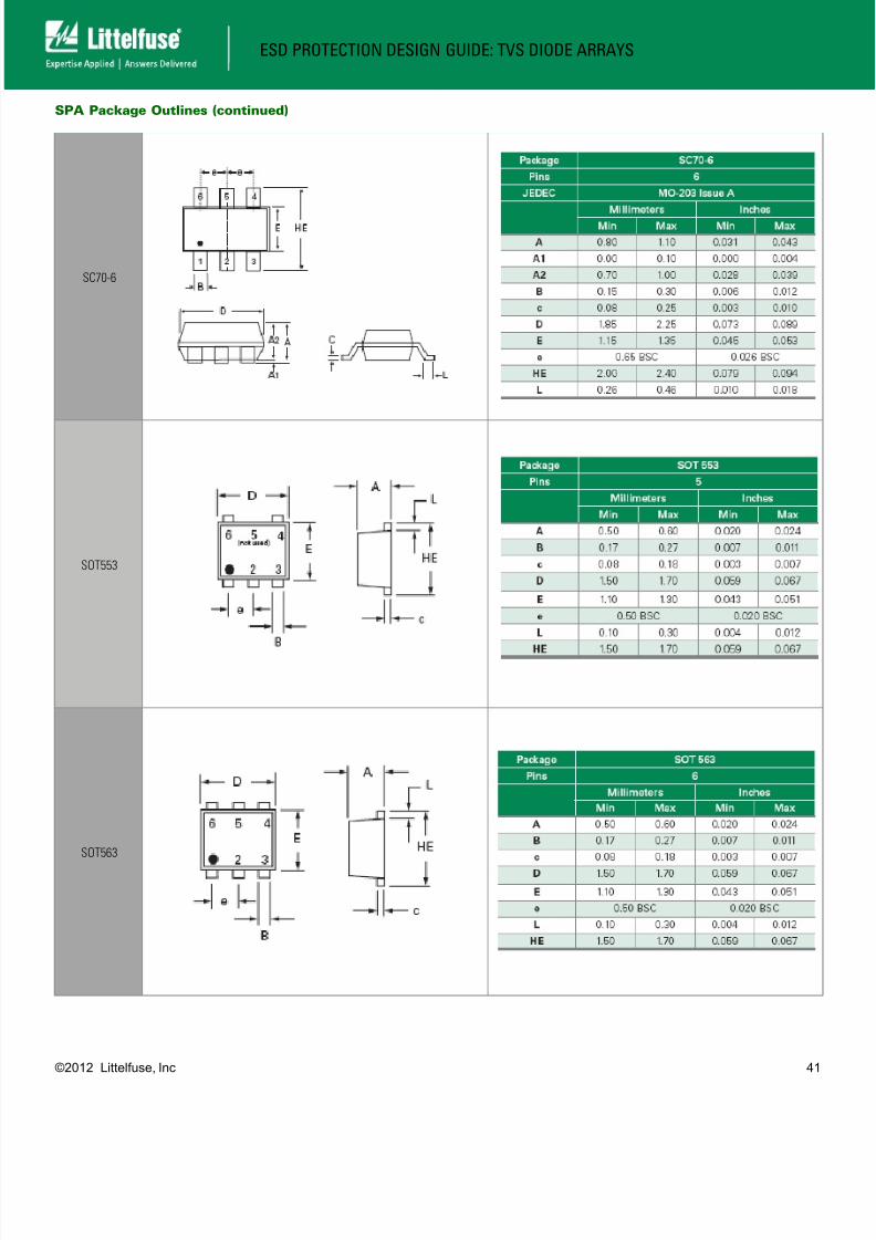
SPA Package Outlines (continued)
SC70-6
SOT553
SOT563
8/10/2019 Littelfuse Esd Protection Design Guide.pdf
http://slidepdf.com/reader/full/littelfuse-esd-protection-design-guidepdf 42/47
ESD PROTECTION DESIGN GUIDE: TVS DIODE ARRAYS
©2012 Littelfuse, Inc 42
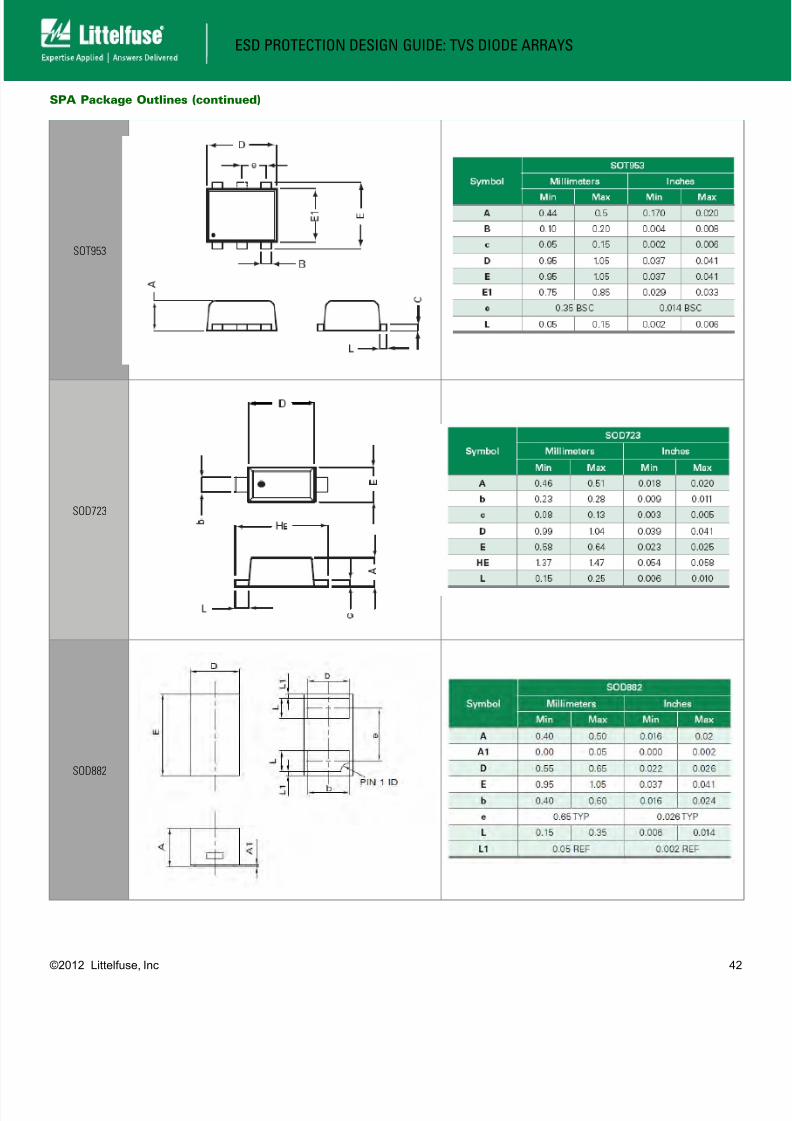
SPA Package Outlines (continued)
SOT953
SOD723
SOD882
8/10/2019 Littelfuse Esd Protection Design Guide.pdf
http://slidepdf.com/reader/full/littelfuse-esd-protection-design-guidepdf 43/47
ESD PROTECTION DESIGN GUIDE: TVS DIODE ARRAYS
©2012 Littelfuse, Inc 43
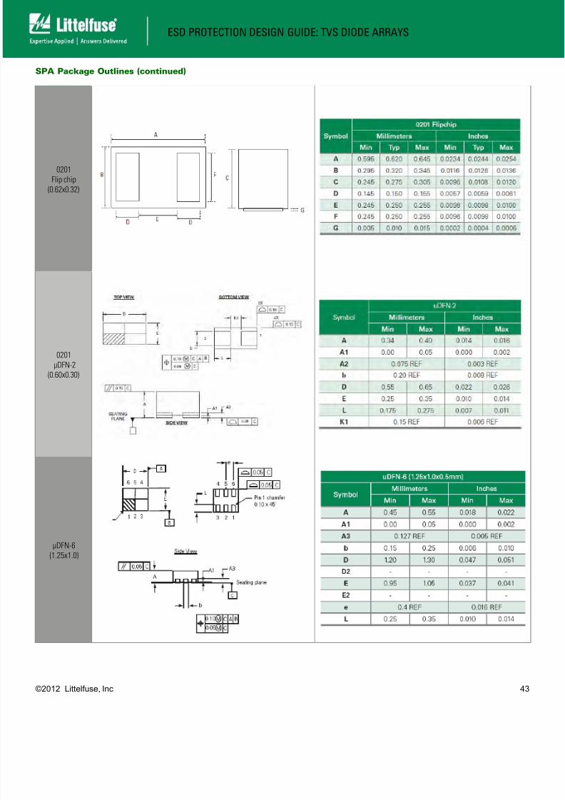
SPA Package Outlines (continued)
0201
Flip chip
(0.62x0.32)
0201
µDFN-2
(0.60x0.30)
μDFN-6
(1.25x1.0)
8/10/2019 Littelfuse Esd Protection Design Guide.pdf
http://slidepdf.com/reader/full/littelfuse-esd-protection-design-guidepdf 44/47
ESD PROTECTION DESIGN GUIDE: TVS DIODE ARRAYS
©2012 Littelfuse, Inc 44
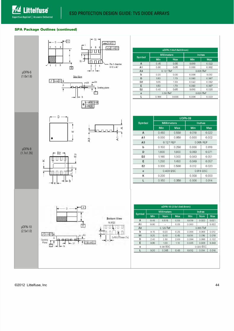
SPA Package Outlines (continued)
μDFN-6
(1.6x1.6)
μDFN-8
(1.7x1.35)
μDFN-10
(2.5x1.0)

8/10/2019 Littelfuse Esd Protection Design Guide.pdf
http://slidepdf.com/reader/full/littelfuse-esd-protection-design-guidepdf 45/47
ESD PROTECTION DESIGN GUIDE: TVS DIODE ARRAYS
©2012 Littelfuse, Inc 45
SPA Package Outlines (continued)
μDFN-10
(2.6x2.6)
μDFN-12
(2.5x1.35)
μDFN-14(3.5x1.35)

8/10/2019 Littelfuse Esd Protection Design Guide.pdf
http://slidepdf.com/reader/full/littelfuse-esd-protection-design-guidepdf 46/47
ESD PROTECTION DESIGN GUIDE: TVS DIODE ARRAYS
©2012 Littelfuse, Inc 46
Littelfuse, Inc.
8755 West Higgins Road
O’Hare Plaza, Suite 500
Chicago, IL 60631 USA
Phone: (773) 628-1000
Authored by:
Chad Marak
Technical Marketing Manager
Semiconductor Business Unit

8/10/2019 Littelfuse Esd Protection Design Guide.pdf
http://slidepdf.com/reader/full/littelfuse-esd-protection-design-guidepdf 47/47
ESD PROTECTION DESIGN GUIDE: TVS DIODE ARRAYS