Mathematical Analysis and Design of Parallel RLC Network ...
45
Mathematical Analysis and Design of Parallel RLC Network in Step-down Switching Power Conversion System Minh Tri Tran a , Yifei Sun b , Noriyuki Oiwa c Yasunori Kobori d , Anna Kuwana e , Haruo Kobayashi f Gunma
Transcript of Mathematical Analysis and Design of Parallel RLC Network ...

Mathematical Analysis and Design of Parallel RLC Network in Step-down Switching Power
Conversion System
Minh Tri Trana, Yifei Sunb, Noriyuki Oiwac
Yasunori Koborid, Anna Kuwanae, Haruo Kobayashif
Gunma

1. Research Background• Applications of Switching Power Supply• Basic Switching Converter Architecture
2. Analysis of Step-down Switching Converter • Conventional Classical Technique• Superposition Principle
3. Proposed Design of Buck Converter• Overshoot Improvement with Parallel RLC Network• Simulation Results
4. Conclusions
Outline

1. Research BackgroundTypical Applications of Switching Power Supply
Switching Converter
DC 12VDC 3VDC 9V
DC 4.2V
DC 9V
DC 3V

Development of switching power supply witho Fast response & high efficiencyo Low EMI noiseo Small output ripple
o Analysis of buck converter system based on classical technique and superposition principleo Overshoot reduction using parallel RLC network
Approach
Objective
1. Research BackgroundResearch Objective & Approach

1. Research BackgroundDesign Achievements
o Derivation of transfer function of buck converter based on superposition principleo Overshoot cancelation based on balanced charge-discharge time condition:
o Overshoot improvement with parallel RLC Overshoot improvement from 1Vpp into 0.1Vppo Ripple reduction using spread spectrum of PWM signals (0.05mVpp)
Achievements
1 12RCLC
2 1 2L CZ Z R L RC

1. Research BackgroundTrade-offs of Switching Power Supply
Linear Regulator
Switching Regulator
Inductive Charge Pump
Efficiency 20-60% 90-95% 75-90%
Ripple Very low Low Moderate
EMI Noise Very low Moderate Low
PCB Area Very small Largest Medium
Cost Lowest Highest Medium

Basic Switching Converter
Meritso Downsizingo Light Weight o High Efficiency
Demeritso Output Ripple o Switching noiseo Harmonic noise
1. Research BackgroundBasic Switching Converter Architecture
RV in
+
V out
–
iL
L
CiC
Ioutiin
High Efficiency SwitchingReduce energy consumptionExtend battery operating timeMinimize costs of systems

1. Research BackgroundSuperposition Principle
n n
i=1 i
i
i i=1A
1 =d d
(t)( EE t)
1d
2d3d
4d5d
6d7d
nd
…
1E (t)
2E (t)
3E (t)4E (t)
5E (t)
6E (t)
7E (t)nE (t)
AE (t)

1. Research BackgroundExample1 of Superposition Principle
R1
V1
L1
~ C1
VA
V3
V2~
~11
1CZ j C
1 1 1 1 1 1
31 21 1 1
C L C LA
V=R Z
VVZ R Z Z
V
1 1 1 1 1
1 1 1 1
31
1
2
1
C L C
C L C LA
VR Z Z R Z=
R Z Z RV
Z ZVV
1 2 31 1 1 1 1 1
1 1 1 1 1A
C L L C
C L C
Z Z R Z RV V V Z=R Z Z
VZ R
21 1 1 1 1
21
1
1 1
2
1
3
1A
j L R LC R=j L R LC R
V V VV
1 1LZ j L

1. Research BackgroundSwitching Regulator
Charge Discharge
arg arg 1( ) ( ) 1 ON
t
Ch e i disch e iV t V t e
ONt OFFt
arg arg( ) ( ) OFF
t
disch e i ch e iV t V t e
outV
ON
out inON OFF
TV VT T
inV Independence of PWM Frequency

1. Research BackgroundSquare Wave Functions
11
1
sin 2 2 14( )2 1k
k tS t
kf
11f T
T
0.5T
time
A
time
A
time
A
0.25T
0.5T
0.25T
0.125T
2 12 2f fT
3 2 14 2 4f f fT
12
1
sin 2 2 214( )2 1k
fk tS t
k
13
1
sin 2 2 414( )2 1k
fk tS t
k
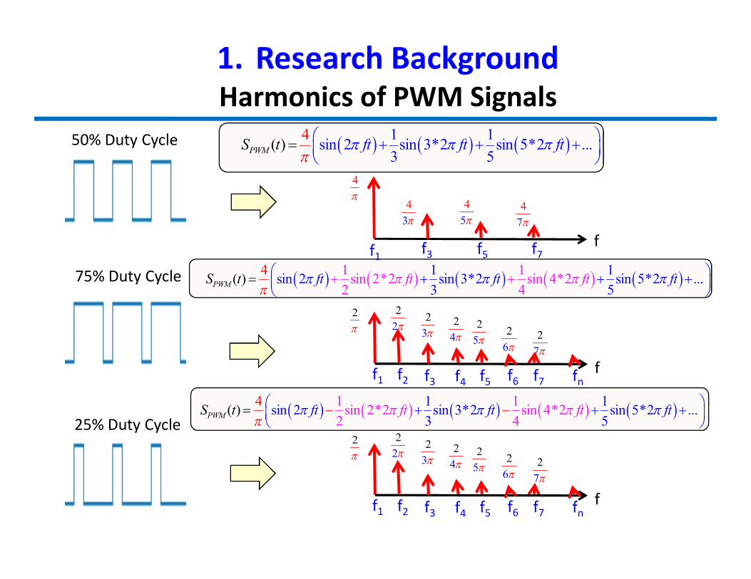
1. Research BackgroundHarmonics of PWM Signals
1 1sin 2 sin 3*2 sin 5*2 ...3 5
( ) 4PWM ft fS t ft t
1 1sin 2 sin 3*21 1sin 2*2 sin 4*22 4
sin 5*2 ...3
4( )5PWM ft fS ft ft fttt
50% Duty Cycle
75% Duty Cycle
25% Duty Cycle
ff1 f2 f3 f4 f5 f6 f7 fn
ff1 f3 f5 f7
1 1sin 2 sin 3*21 1sin 2*2 sin 4*22 4
sin 5*2 ...3
4( )5PWM ft fS ft ft fttt
4
43
45
47
2
22
23
24
25
26
27
ff1 f2 f3 f4 f5 f6 f7 fn
2
22
23
24
25
26
27

1. Research Background• Applications of Switching Power Supply• Basic Switching Converter Architecture
2. Analysis of Step-down Switching Converter • Conventional Classical Technique• Superposition Principle
3. Proposed Design of Buck Converter• Overshoot Improvement with Parallel RLC Network• Simulation Results
4. Conclusions
Outline

2. Analysis of Step-down Switching ConverterConventional Classical Technique
CapacitorInductor
0
0
00
1 1( ) ( ) ( )
1( ) ( )
t t
t
t
t
v t i d i dc c
v t i dc
0
0
00
1 1( ) ( ) ( )
1( ) ( )
t t
t
t
t
i t v d v dL L
i t v dL
Magnetic energy Electric energy
• Advantages– Converts differential equation into algebraic equation.– Rapidly provides stability & transient response.
• Disadvantages– Applicable only to Linear, Time-Invariant (LTI) systems
LC( )i t ( )v t
+ -

RVin
+
Vout
–
iL
L
CiC
Ioutiin ON
charge
DOFF
( ) ( ) ( )L out Ci t I t i t
0
( )( )( ) 1( ) ; ( ) ; ( ; ( )) ( )ON
out out C L
Toutout
oui tn
dQ tV t I t i t CV tV i t V dtV
C R d Lt t
t
0
( ) ( ) 1 ( )ONT
out outi outn
dC V dtR dt
VL
V t V t t
0 0
( ) ( )( )1 1ON ONT Tout o t
u inu
o tV t V tddt C V dtR L L
Vdt
t 2
2
( ) ( ) (1 0)out out outV t V t V td dCR dt L dt
2
2
( ) ( ) ( )1 0out out outd ddt RC dtV t V
Ct V t
L
2. Analysis of Step-down Switching ConverterAnalysis of Buck Converter (Switch ON)

2
2
( ) ( ) ( )1 0out out outd ddt RC dtV t V
Ct V t
L
1 21 2( )o
tu
s s tstt Ae A et AV e
2
2 01st st std Ae d Ae Ae
dt RC dt LC
2 1 01s sRC LC
2 2
1 21 1 1 1 1 1
2 2 2 2s s
RC RC LC RC RC LC
21 1; ;
2RC LCRC LC
2 22 2
2 22 2
arg 1 2( )RC RC LC RC RC LCt t
ch e ch chV et A e A
2. Analysis of Step-down Switching ConverterAnalysis of Buck Converter (Switch ON)

RV in
+
Vout
–
iL
L
CiC
IoutOFF
discharge
DON
( ) ( ) ( )out L CI t i t i t
( ) 1; ( ) ; ( ) ; ( )( )( )( ) ( )
O
F
N
OFTdis
out C L diodis
d dis di esT
dQ t I t i t C i tV tV tV t V V dt
C R dt Lt
( ) ( ) ( )1 OF
ON
FTdis
dioded
T
isdis
V t V t VdC V dtR dt
tL
( ) ( ) ( )1 1OFF
O
FF
N
O
ONT
T Tdis d
dios
dei
dT
isV t VdC dt V dt V t tdt R L L
1( ) ( ) ) 0(OFF
ON
dis dis
Tdi
T
sdC V t V t dt
RV t
dt L
2
2
( ) ( ) ( )1 0dis dis disd ddt RC dt
VC
V t V t tL
2. Analysis of Step-down Switching ConverterAnalysis of Buck Converter (Switch OFF)

2
2
( ) ( ) ( )1 0dis dis disd ddt RC dt
VC
V t V t tL
1 23 3( ) dis diss t s ts
dis dit
sA e A e A eV t
2
2 01dis dist st
s isst
dd A e d A e A edt RC dt LC
2 1 01s sRC LC
2 2
1 21 1 1 1 1 1
2 2 2 2dis diss sRC RC LC RC RC LC
21 1; ;
2RC LCRC LC
2 22 2 2 2
2 2
rg 1 2a ( )RC RC LC RC RC LCt t
dich ed s di s isV t A e A e
2. Analysis of Step-down Switching ConverterAnalysis of Buck Converter (Switch OFF)

2 22 2 2 2
2 22 2 2
2
2 22
2
0
1
1
2
21
RC RCON
O
LC RC RC LC
RC RC LC RFF
O
C RC LC
N
T t t
out T t tON OFFdis di
ch
T
c
s
hA e A e dt
VT T
A e A e dt
21 1
2RC LC RCLC
1 2L RC
0
1 ON OFF
ON
c
T Tt t
out disON OFF
hT
V A e dt A e dtT T
2. Analysis of Step-down Switching ConverterBalanced Charge-Discharge Time Condition
2L CZ Z R
Balanced Charge-Discharge Time Condition

LZ j L
1cZ j CVin
Vout
RL
2. Analysis of Step-down Switching ConverterProposed Analysis Model of Buck Converter
RV in
+
Vout
–
iL
L
CiC
Ioutiin ON
charge
DOFF
RVin
+
Vout
–
iL
L
CiC
IoutOFF
discharge
DON
Model of Buck Converter
( )PWMS t
Switch OFFSwitch ON

LZ j L
1cZ j CVin
Vout
RL
2
1
1 1LCH j
j jRC LC
1 1 1
Co in
L C
ino
L C
L C L
VVZ Z R Z
RZV VR Z Z Z Z
o C
in L C L C
V RZHV R Z Z Z Z
2. Analysis of Step-down Switching ConverterTransfer Function of Proposed Analysis Model
Transfer Function
Output Voltage
Superpositionprinciple
Proposed analysis model

2
1
1 1LCH j
j jRC LC
2
22
12
2 1 12 2
LCH j f
j f j fRC LC
2
2 22
2
12
122
LCH f
ffRCLC
2
22
12 1 1
4 214
12
H f H f whenLC
fRC LC
fRC
2L CZ Z R
2. Analysis of Step-down Switching ConverterMax Power Propagation Condition
Balanced Charge-Discharge Time Condition
Transfer Function

2. Analysis of Step-down Switching ConverterSimulation of Un-balanced Charge-discharge Time
2L CZ Z R
1 ; 2 2L CZ Z R _1 1 /cut off rad sLC
with overshoot voltage

2L CZ Z R
2. Analysis of Step-down Switching ConverterSimulation of Balanced Charge-discharge Time
1 ; 2 1L CZ Z R _1 1 /cut off rad sLC
w/o overshoot voltage

1. Research Background• Applications of Switching Power Supply• Basic Switching Converter Architecture
2. Analysis of Step-down Switching Converter • Conventional Classical Technique• Superposition Principle
3. Proposed Design of Buck Converter• Overshoot Improvement with Parallel RLC Network• Simulation Results
4. Conclusions
Outline

Modify
Modulate
Circuit with Frequency Modulation
3. Proposed Design of Buck Converter Conventional Step-down Switching Converter
VCO:Voltage Controlled Oscillator
VCO
Input Voltage (Vin) 12V
Output Voltage (Vo) 5.0V
Output Current (Io) 1.0A
Clock Frequency (Fck) 200kHz
EMI Reduction using Spread Spectrum of VCO

( )VCO VCO mt t t
K: sensitivity of VCOVb: bias voltageVm: modulation signal
SAW VCO
Vm
Vb
PWM
ModulationSignal
cos ( )VCO VCO VCO mS t A t t
( ) cos(2 )m m mm V t A fKt K t
( ) cos(2 )m m mV t A f tVCO bVK
cos ( )VCO VCO VCOS t A tFrequency Modulation function:
cos(2 )m mVCO b AK ft V t tK
3. Proposed Design of Buck Converter Frequency Modulation of VCO

time
A
2 2 4 6
0
1cos 1
2 ! 2! 4! 6!
k k
k
x x x xxk
2
0
2 4 6
( ) cos 2
1 22 !
2 2 21
2! 4! 6!
m m m
k km
k
m m m
V t A f t
f tk
f t f t f t
cos ( )VCO VCO VCO mS t A t t
2
0
2 4 6
cos(2 )
1 22 !
2 2 21
2! 4! 6!
VCO b
k km
bk
m m mb
m m
m
m
t V t
f tV t
k
f t f t f t
K K
K
A f t
tK K
A
A
K
V
Frequency Modulation function:
frequency
A
VCOf
Spread spectrum VCO mf f
3. Proposed Design of Buck Converter Spectrum of VCO Signals

2 4 6
cos ( )
2 2 2cos 1
2! 4! 6!
VCO VCO VCO m
m m mV mCO b
S t A t t
f t f t f tA KV AtK
50% Duty Cycle
75% Duty Cycle
25% Duty Cycle
ff1 f3 f5 f7
4
43
45
47
ff1 f2 f3 f4 f5 f6 f7 fn
2
22
23
24
25
26
27
ff1 f2 f3 f4 f5 f6 f7 fn
2
22
23
24
25
26
27
V C O mf f
3. Proposed Design of Buck Converter Spread Spectrum of PWM Signals

3. Proposed Design of Buck Converter Simulation of Conventional Buck Converter
_1 5
2cut offf kHzLC
Frequency Modulation
of VCO Signal
5totalR
10L CZ Z 2L CZ Z R

5 us
Overshoot Voltage
3. Proposed Design of Buck Converter Waveforms of Conventional Buck Converter
Transient state Stable state
Ripple voltages
Spectrum of ripple voltages

Modify
Modulate
R2
L2
C2C1
L1RL Overshoot
Improvement
EMI Reduction using Spread
Spectrum of VCO
3. Proposed Design of Buck Converter Proposed Design of Step-down Switching Converter

R2
L2
C2Vin
Vout
RL
1 1LZ j L
L1
C11
1
1CZ j C
D1
1 1 2 2 2 1
1 1 1 1 ino
L C L L C L
VVZ Z R R Z Z Z
2 2 2 1
2 2 2 1 1 1 1 1 1
L C L Lo in
L C L L C L C L C L
Z Z R Z RV V
Z Z R R Z Z Z Z Z Z R
2 2 2 1
2 2 2 1 1 1 1 1 1
L C L Lo
in L C L L C L C L C L
Z Z R Z RVHV Z Z R R Z Z Z Z Z Z R
2 2
1 1 2 2 22
2 22
2 2 2 1 1 1 2 1
1 1
1 1 1L
Rj jLC L L C
H jjRj j j j
L L C R C LC L C
Transfer Function
Output Voltage
Superpositionprinciple
Proposed model Overshoot Reduction
3. Proposed Design of Buck Converter Overshoot Improvement with Parallel RLC Network

Over-shoot
Over-shoot Reduction
3. Proposed Design of Buck Converter Simulation of Parallel RLC Network
10 2 40L CZ Z R Cutoff frequency
_1 5
2cut offf kHzLC
10 ;2 40L CZ ZR

5f KHz
Over-shoot
Over-shoot
Reduction
3. Proposed Design of Buck Converter Frequency Response of Parallel RLC Network
Cutoff frequency
2L CZ Z R

Over-shoot
Over-shoot
Reduction
3. Proposed Design of Buck Converter Transient Response of Parallel RLC Network
2L CZ Z R
Power On Operation times
Transient state Stable state

VIN
VOUT
RLD1
PWM Controller
L
C
Feedback
Q1 onC charges
+ - R2
L2C2
(a)
- +
L reverses polarityoff
VIN
VOUT
RLD1
L
C
Feedback
Q1
PWM Controller
R2
L2C2
(b)
R f
C f
VVcontrol set
outV
(c)
1 1 control ou
f ffs t
f
te
VVZ R
VZ R
1set set ocontrol ut set set
Cut
f fo
f
f
V V V VZR j C R
V VV
Keep small difference
Feedback Voltage Control
3. Proposed Design of Buck Converter Analysis of Feedback Voltage Control

3. Proposed Design of Buck Converter Proposed Design of Step-down Switching Converter
Overshoot Reduction
Frequency Modulation
of VCO Signal
_ 5cut offf kHz _ 5par RLCf kHz

Overshoot Voltage>1 Vpp
Overshoot VoltageReduction< 0.1 Vpp
3. Proposed Design of Buck Converter Overshoot Reduction Waveforms
Transient state Stable statewithout parallel RLC network
with parallel RLC network

2 10MHzV uV4 3MHzV uV
0.05mVpp
• Input Voltage (Vin): 12V• Output Voltage (Vo): 5.0V• Output Current (Io): 1A• Clock Frequency (Fck): 200kHz• Overshoot: 0.1V• Ripple Voltage: 0.05mVpp
3. Proposed Design of Buck Converter Waveforms of Proposed Buck Converter
Transient state Stable state
Ripple voltages Spectrum of ripple voltages

1. Research Background• Applications of Switching Power Supply• Basic Switching Converter Architecture
2. Analysis of Step-down Switching Converter • Conventional Classical Technique• Superposition Principle
3. Proposed Design of Buck Converter• Overshoot Improvement with Parallel RLC Network• Simulation Results
4. Conclusions
Outline

This work:• Balanced charge-discharge time condition
• Analysis model of Buck converter system based on classical technique and superposition principle
• Overshoot improvement with parallel RLC network Overshoot reduction from 1Vpp into 0.1Vpp
Future of Work• Analysis of parasitic of RLC and other components
4. Conclusions
1 12RCLC
2 1 2L CZ Z R L RC

Thanks for your kind attention!

Questions & Answers1) Why was the balanced charge-discharge time
condition introduced in this research?Because the overshoot phenomena will be detected if this balanced condition is not satisfied.(Based on the selection of R, L and C components, the overshoot voltage can be perfectly controlled.)
2) Was the source code program written to simulate the parallel low-pass filter of Buck converter on Mat-labs? No, it wasn’t.(There is a stool on Mat-labs to simulate this filter.)