
Materials Characterization || Transmission Electron Microscopy
41
3 Transmission Electron Microscopy Electron microscopes generate images of material microstructures with much higher magni- fication and resolution than light microscopes. The high resolution of electron microscopes results from short wavelengths of the electrons used for microscope illumination. The wave- length of electrons in electron microscopes is about 10,000 times shorter than that of visible light. The resolution of electron microscopes reaches the order of 0.1 nm if lens aberra- tions can be minimized. Such high resolution makes electron microscopes extremely use- ful for revealing ultrafine details of material microstructure. There are two main types of electron microscopes: transmission electron microscopes (TEM) and scanning electron mi- croscopes (SEM). The optics of the TEM is similar to the conventional transmission light microscope, while that of SEM is more like that of scanning confocal laser microscopes. This chapter introduces the basic working principles and features of transmission electron microscopes. 3.1 Instrumentation A transmission electron microscope, similar to a transmission light microscope, has the fol- lowing components along its optical path: light source, condenser lens, specimen stage, ob- jective lens and projector lens as shown in Figure 3.1. The main differences are that, in a TEM, the visible light ray is replaced by an electron ray and glass lenses for visible light are replaced by electromagnetic lens for the electron beam. The TEM has more lenses (the intermediate lens) and more apertures (including the selected area aperture). The TEM con- tains further features arising from using electrons as illumination. For example, a vacuum environment is required in a TEM because collisions between high energy electrons and air molecules significantly absorb electron energy. Table 3.1 provides a comparison of a TEM with a light microscope. Structural features of the TEM are introduced in detail in the following sections. Materials Characterization: Introduction to Microscopic and Spectroscopic Methods Yang Leng © 2008 John Wiley & Sons (Asia) Pte Ltd. ISBN: 978-0-470-82298-2
Transcript of Materials Characterization || Transmission Electron Microscopy
3Transmission ElectronMicroscopy
Electron microscopes generate images of material microstructures with much higher magni-fication and resolution than light microscopes. The high resolution of electron microscopesresults from short wavelengths of the electrons used for microscope illumination. The wave-length of electrons in electron microscopes is about 10,000 times shorter than that of visiblelight. The resolution of electron microscopes reaches the order of 0.1 nm if lens aberra-tions can be minimized. Such high resolution makes electron microscopes extremely use-ful for revealing ultrafine details of material microstructure. There are two main types ofelectron microscopes: transmission electron microscopes (TEM) and scanning electron mi-croscopes (SEM). The optics of the TEM is similar to the conventional transmission lightmicroscope, while that of SEM is more like that of scanning confocal laser microscopes.This chapter introduces the basic working principles and features of transmission electronmicroscopes.
3.1 Instrumentation
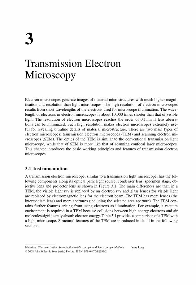
A transmission electron microscope, similar to a transmission light microscope, has the fol-lowing components along its optical path: light source, condenser lens, specimen stage, ob-jective lens and projector lens as shown in Figure 3.1. The main differences are that, in aTEM, the visible light ray is replaced by an electron ray and glass lenses for visible lightare replaced by electromagnetic lens for the electron beam. The TEM has more lenses (theintermediate lens) and more apertures (including the selected area aperture). The TEM con-tains further features arising from using electrons as illumination. For example, a vacuumenvironment is required in a TEM because collisions between high energy electrons and airmolecules significantly absorb electron energy. Table 3.1 provides a comparison of a TEM witha light microscope. Structural features of the TEM are introduced in detail in the followingsections.
Materials Characterization: Introduction to Microscopic and Spectroscopic Methods Yang Leng
© 2008 John Wiley & Sons (Asia) Pte Ltd. ISBN: 978-0-470-82298-2
80 Materials Characterization
Table 3.1 Comparison Between Light and Transmission Electron Microscopes
Transmission electronTransmission light microscope microscope
Specimen requirements Polished surface and thin section(<100 µm)
Thin section (<200 nm)
Best resolution ∼200 nm ∼0.2 nmMagnification range 2–2000× 500–1,000,000×Source of illumination Visible light High-speed electronsLens Glass ElectromagneticOperation environment Air or liquid High vacuumImage formation for viewing By eye On phosphorescent plate
Illumination
Specimen stage
Imaging
Magnification
Projector lens
Intermediate lens
Specimen
2nd condenser lens
1st condenser lens
Accelerator
Electron gun
High vacuum
Objective lens
Data recording
Fluorescent screenPhotographic filmCCD camera
Figure 3.1 Structure of a transmission electron microscope and the optical path.
Transmission Electron Microscopy 81
Table 3.2 Correlation between Acceleration Voltage and Resolution
Acceleration voltage (kV) Electron wavelength (nm) TEM resolution (nm)
40 0.00601 0.5660 0.00487 0.4680 0.00418 0.39
100 0.00370 0.35200 0.00251 0.24500 0.00142 0.13
3.1.1 Electron Sources
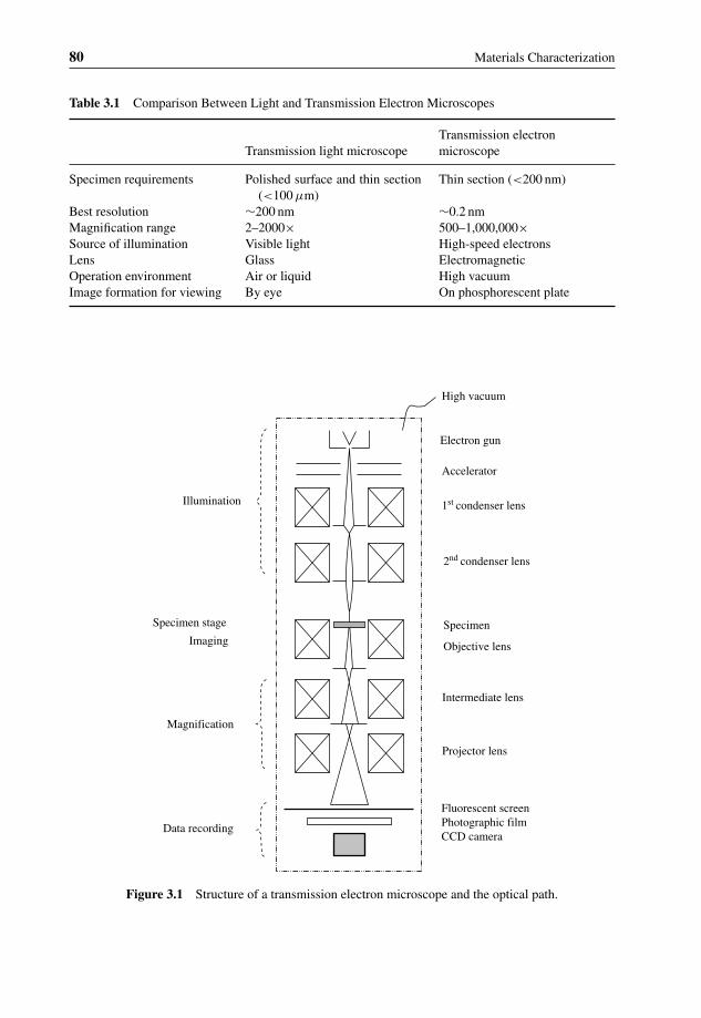
In a TEM system, an electron gun generates a high energy electron beam for illumination.In the electron gun, the electrons emitted from a cathode, a solid surface, are accelerated byhigh voltage (Vo) to form a high energy electron beam with energy E = eVo. Because electronenergy determines the wavelength of electrons and wavelength largely determines resolutionof the microscope (Equation 1.3), the acceleration voltage determines the resolution to a largeextent. Table 3.2 gives the relationship between the acceleration voltage and wavelength. Italso provides the correlation between acceleration voltage and the TEM resolution, which iscalculated with a realistic α angle of about 6.5 × 10⁻³ radians. To achieve a high resolution,the TEM is usually operated under an acceleration voltage of greater than 100 kV. In practice,200 kV is commonly used and meets most resolution requirements. High-voltage electronmicroscopy (∼1000 kV) requires extremely expensive instrumentation, and also it may damagea specimen by generating microstructural defects in it during observation.
The general structure of an electron gun is composed of three main parts: cathode or electronsource, Wehnelt electrode and anode, as illustrated in Figure 3.2. Electrons are emitted fromthe surface of the cathode and accelerated by an electric field toward the cathode. The Wehneltelectrode is placed between the cathode and the anode. It is biased a few hundred volts negativewith respect to the cathode in order to stabilize the electron beam against voltage fluctuation by
Cathode
Wehneltelectrode
Anode
Figure 3.2 General structure of an electron gun.
82 Materials Characterization
reducing the electron beam current whenever necessary. There are two basic types of electronguns: thermionic emission and field emission.
Thermionic Emission GunThis is the most common type of electron gun and includes the tungsten filament gun and thelanthanum hexaboride gun. The tungsten gun uses a tungsten filament as the cathode. Duringoperation, the filament is heated by electrical current (filament current) to high temperature(∼2800 K). The high temperature provides kinetic energy for electrons to overcome the surfaceenergy barrier, enabling the conduction electrons in the filament to leave the surface. Theelectrons leaving the surface are accelerated by a high electric voltage between the filamentand anode to a high energy level. The intensity of the electron beam is determined by thefilament temperature and acceleration voltage.
Lanthanum hexaboride (LaB6) is a better cathode than tungsten and it is more widely usedin modern electron microscopes. Electrons require less kinetic energy to escape from the LaB6surface because its surface work function is about 2 eV, smaller than the 4.5 eV of tungsten.Thus, a lower cathode temperature is required. A LaB6 cathode can generate a higher intensityelectron beam and has a longer life than a tungsten filament. One disadvantage is that a higherlevel of vacuum is required for a LaB6 gun than for a tungsten filament gun.
Field Emission GunThis type of electron gun does not need to provide thermal energy for electrons to overcomethe surface potential barrier of electrons. Electrons are pulled out by applying a very highelectric field to a metal surface. A tunneling effect, instead of a thermionic effect, makes metalelectrons in the conducting band cross the surface barrier. During operation, electrons arephysically drawn off from a very sharp tip of tungsten crystal (∼100 nm tip radius) by anapplied voltage field. The field emission gun generates the highest intensity electron beam,104 times greater than that of the tungsten filament gun and 102 times greater than that of theLaB6 gun. There are two kinds of field emission guns: thermal and cold guns. The thermalfield emission gun works at an elevated temperature of about 1600–1800 K, lower than thatof thermionic emission. It provides a stable emission current with less emission noise. Thecold field emission gun works at room temperature. It provides a very narrow energy spread(about 0.3–0.5 eV), but it is very sensitive to ions in air. The bombardment of the tungsten tipby residual gaseous ions causes instability of the emission. Thus, regular maintenance (calledflashing) of the tip is necessary. Generally, a vacuum of 10−10 torr is required to operate thecold field emission gun. Table 3.3 shows a comparison of various kinds of electron guns.
Table 3.3 Comparison of Electron Guns
Field emissionTungstenThermal Coldfilament LaB6
Operation temperature (K) ∼2800 ∼1800 1600 ∼ 1800 ∼300Brightnessa At 200 kV (A cm−2 sr) ∼5 × 10⁵ ∼5 × 10⁶ ∼5 × 10⁸ ∼5 × 10⁸
Requirement to vacuum (Torrb) 10−4 10−6–10−7 10−9 10−9–10−10
a Intensity emitted per unit cathode surface in unit solid angle.b 1 torr = 133 Pa.
Transmission Electron Microscopy 83
3.1.2 Electromagnetic Lenses
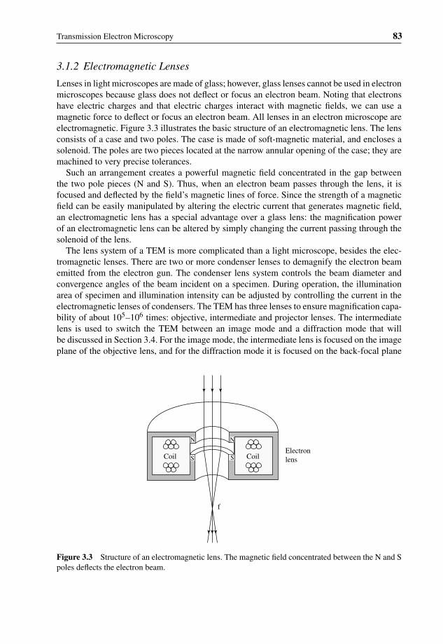
Lenses in light microscopes are made of glass; however, glass lenses cannot be used in electronmicroscopes because glass does not deflect or focus an electron beam. Noting that electronshave electric charges and that electric charges interact with magnetic fields, we can use amagnetic force to deflect or focus an electron beam. All lenses in an electron microscope areelectromagnetic. Figure 3.3 illustrates the basic structure of an electromagnetic lens. The lensconsists of a case and two poles. The case is made of soft-magnetic material, and encloses asolenoid. The poles are two pieces located at the narrow annular opening of the case; they aremachined to very precise tolerances.
Such an arrangement creates a powerful magnetic field concentrated in the gap betweenthe two pole pieces (N and S). Thus, when an electron beam passes through the lens, it isfocused and deflected by the field’s magnetic lines of force. Since the strength of a magneticfield can be easily manipulated by altering the electric current that generates magnetic field,an electromagnetic lens has a special advantage over a glass lens: the magnification powerof an electromagnetic lens can be altered by simply changing the current passing through thesolenoid of the lens.
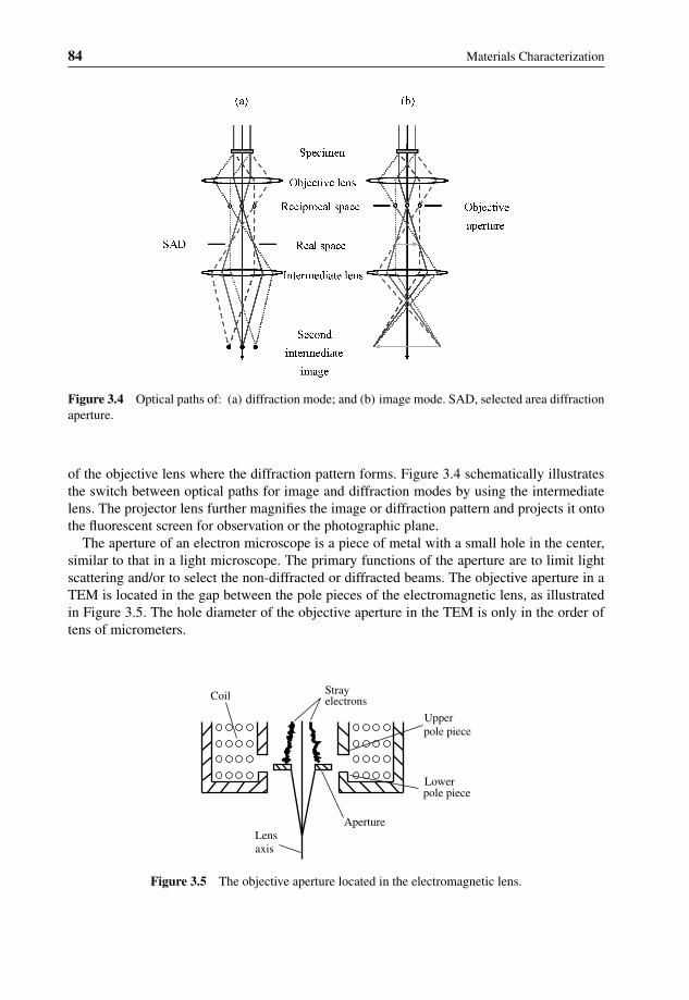
The lens system of a TEM is more complicated than a light microscope, besides the elec-tromagnetic lenses. There are two or more condenser lenses to demagnify the electron beamemitted from the electron gun. The condenser lens system controls the beam diameter andconvergence angles of the beam incident on a specimen. During operation, the illuminationarea of specimen and illumination intensity can be adjusted by controlling the current in theelectromagnetic lenses of condensers. The TEM has three lenses to ensure magnification capa-bility of about 105–106 times: objective, intermediate and projector lenses. The intermediatelens is used to switch the TEM between an image mode and a diffraction mode that willbe discussed in Section 3.4. For the image mode, the intermediate lens is focused on the imageplane of the objective lens, and for the diffraction mode it is focused on the back-focal plane
Coil CoilElectronlens
f
NN
SS
Figure 3.3 Structure of an electromagnetic lens. The magnetic field concentrated between the N and Spoles deflects the electron beam.
84 Materials Characterization
Figure 3.4 Optical paths of: (a) diffraction mode; and (b) image mode. SAD, selected area diffractionaperture.
of the objective lens where the diffraction pattern forms. Figure 3.4 schematically illustratesthe switch between optical paths for image and diffraction modes by using the intermediatelens. The projector lens further magnifies the image or diffraction pattern and projects it ontothe fluorescent screen for observation or the photographic plane.
The aperture of an electron microscope is a piece of metal with a small hole in the center,similar to that in a light microscope. The primary functions of the aperture are to limit lightscattering and/or to select the non-diffracted or diffracted beams. The objective aperture in aTEM is located in the gap between the pole pieces of the electromagnetic lens, as illustratedin Figure 3.5. The hole diameter of the objective aperture in the TEM is only in the order oftens of micrometers.
Lensaxis
Aperture
Lower
Upper
StrayCoil electrons
pole piece
pole piece
Figure 3.5 The objective aperture located in the electromagnetic lens.

Transmission Electron Microscopy 85
Figure 3.6 A specimen holder for a TEM (JEM-2010F) with a double-tilting function. The insert showsthe enlarged part of the holder end where the 3-mm disc of the specimen is installed.
3.1.3 Specimen Stage
The TEM has special requirements for specimens to be examined; it does not have the sameflexibility in this regard as light microscopy. TEM specimens must be a thin foil because theyshould be able to transmit electrons; that is, they are electronically transparent. A thin specimenis mounted in a specimen holder, as shown in Figure 3.6, in order to be inserted into the TEMcolumn for observation. The holder requires that a specimen is a 3-mm disc. Smaller specimenscan be mounted on a 3-mm mesh disc as illustrated in Figure 3.7. The meshes, usually madefrom copper, prevent the specimens from falling into the TEM vacuum column. Also, a coppermesh can be coated with a thin film of amorphous carbon in order to hold specimen pieceseven smaller than the mesh size.
Figure 3.7 A metal mesh disc supporting small foil pieces of specimen.

86 Materials Characterization
The specimen holder is a sophisticated, rod-like device that not only holds the specimen butalso is able to tilt it for better viewing inside the TEM column. Types of specimen holders usedinclude single-tilt and double-tilt. The single-tilt holder allows a specimen to be titled alongone axis in the disc plane. The double-tilt holder allows the specimen be tilted independentlyalong two axes in the disc plane. The double-tilt holder is necessary for analytical studies ofcrystalline structures.
3.2 Specimen Preparation
Preparation of specimens often is the most tedious step in TEM examination. To be electroni-cally transparent, the material thickness is limited. We have to prepare a specimen with at leastpart of its thickness at about 100 nm, depending on the atomic weight of specimen materials.For higher atomic weight material, the specimen should be thinner. A common procedure forTEM specimen preparation is described as follows.
3.2.1 Pre-Thinning
Pre-thinning is the process of reducing the specimen thickness to about 0.1 mm before finalthinning to 100 nm thickness. First, a specimen less than 1 mm thick is prepared. This is usuallydone by mechanical means, such as cutting with a diamond saw. Then, a 3-mm-diameter disc iscut with a specially designed punch before further reduction of thickness. Grinding is the mostcommonly used technique to reduce the thickness of metal and ceramic specimens. Duringgrinding, we should reduce thickness by grinding both sides of a disc, ensuring the planes areparallel. This task would be difficult without special tool. Figure 3.8 shows a hand-grindingjig for pre-thinning. The disc (S) is glued to the central post and a guard ring (G) guides thegrinding thickness. A dimple grinder is also used for pre-thinning, particularly for specimensthat are finally thinned by ion milling, which is introduced in Section 3.2.2.
Figure 3.8 Hand-grinding jig for TEM specimen preparation. A disc (S) is glued to the center of thejig and the guide ring (G) controls the amount of grinding.
Transmission Electron Microscopy 87
Figure 3.9 A dimple in the center of a specimen disc.
3.2.2 Final Thinning
Three methods of final thinning are described here: electrolytic thinning for metal specimensthat are good electric conductors, ion milling for metal and ceramic specimens, and ultra-microtome cutting for polymeric and biological specimens.
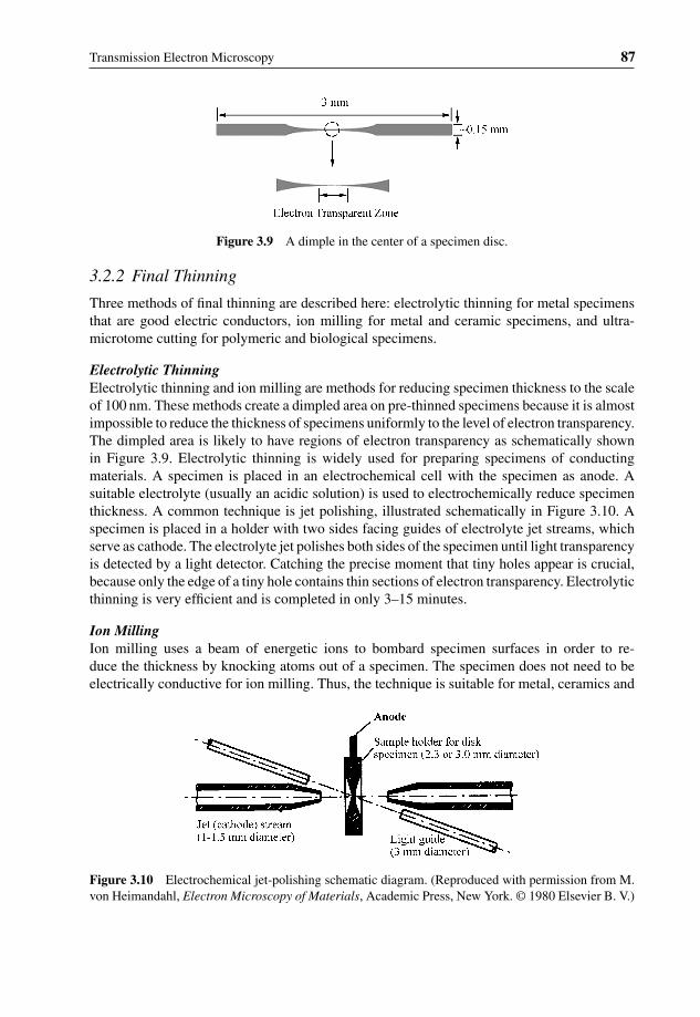
Electrolytic ThinningElectrolytic thinning and ion milling are methods for reducing specimen thickness to the scaleof 100 nm. These methods create a dimpled area on pre-thinned specimens because it is almostimpossible to reduce the thickness of specimens uniformly to the level of electron transparency.The dimpled area is likely to have regions of electron transparency as schematically shownin Figure 3.9. Electrolytic thinning is widely used for preparing specimens of conductingmaterials. A specimen is placed in an electrochemical cell with the specimen as anode. Asuitable electrolyte (usually an acidic solution) is used to electrochemically reduce specimenthickness. A common technique is jet polishing, illustrated schematically in Figure 3.10. Aspecimen is placed in a holder with two sides facing guides of electrolyte jet streams, whichserve as cathode. The electrolyte jet polishes both sides of the specimen until light transparencyis detected by a light detector. Catching the precise moment that tiny holes appear is crucial,because only the edge of a tiny hole contains thin sections of electron transparency. Electrolyticthinning is very efficient and is completed in only 3–15 minutes.
Ion MillingIon milling uses a beam of energetic ions to bombard specimen surfaces in order to re-duce the thickness by knocking atoms out of a specimen. The specimen does not need to beelectrically conductive for ion milling. Thus, the technique is suitable for metal, ceramics and
Figure 3.10 Electrochemical jet-polishing schematic diagram. (Reproduced with permission from M.von Heimandahl, Electron Microscopy of Materials, Academic Press, New York. © 1980 Elsevier B. V.)
88 Materials Characterization
Glass
Specimen
Grinder
Diamond paste
(a)
Laserautoterminator
Specimen
Laser light
Mo mesh
Ar ion
(b)
Figure 3.11 Ion thinning process: (a) dimple grinding; and (b) ion milling. (Reproduced with kindpermission of Springer Science and Business Media from D. Shindo and T. Oikawa, Analytical ElectronMicroscopy for Materials Science, Springer-Verlag, Tokyo. © 2002 Springer-Verlag GmbH.)
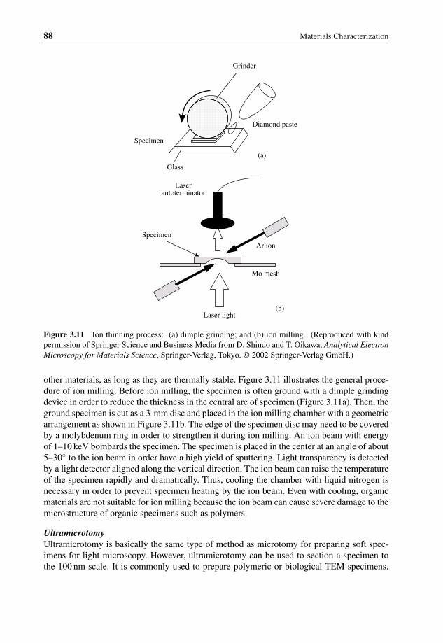
other materials, as long as they are thermally stable. Figure 3.11 illustrates the general proce-dure of ion milling. Before ion milling, the specimen is often ground with a dimple grindingdevice in order to reduce the thickness in the central are of specimen (Figure 3.11a). Then, theground specimen is cut as a 3-mm disc and placed in the ion milling chamber with a geometricarrangement as shown in Figure 3.11b. The edge of the specimen disc may need to be coveredby a molybdenum ring in order to strengthen it during ion milling. An ion beam with energyof 1–10 keV bombards the specimen. The specimen is placed in the center at an angle of about5–30◦ to the ion beam in order have a high yield of sputtering. Light transparency is detectedby a light detector aligned along the vertical direction. The ion beam can raise the temperatureof the specimen rapidly and dramatically. Thus, cooling the chamber with liquid nitrogen isnecessary in order to prevent specimen heating by the ion beam. Even with cooling, organicmaterials are not suitable for ion milling because the ion beam can cause severe damage to themicrostructure of organic specimens such as polymers.
UltramicrotomyUltramicrotomy is basically the same type of method as microtomy for preparing soft spec-imens for light microscopy. However, ultramicrotomy can be used to section a specimen tothe 100 nm scale. It is commonly used to prepare polymeric or biological TEM specimens.
Transmission Electron Microscopy 89
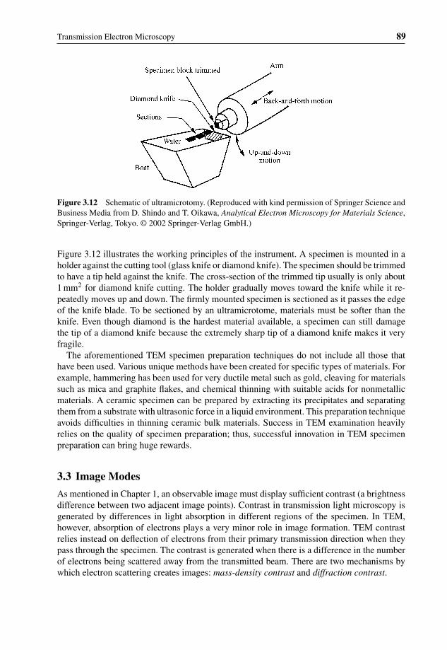
Figure 3.12 Schematic of ultramicrotomy. (Reproduced with kind permission of Springer Science andBusiness Media from D. Shindo and T. Oikawa, Analytical Electron Microscopy for Materials Science,Springer-Verlag, Tokyo. © 2002 Springer-Verlag GmbH.)
Figure 3.12 illustrates the working principles of the instrument. A specimen is mounted in aholder against the cutting tool (glass knife or diamond knife). The specimen should be trimmedto have a tip held against the knife. The cross-section of the trimmed tip usually is only about1 mm2 for diamond knife cutting. The holder gradually moves toward the knife while it re-peatedly moves up and down. The firmly mounted specimen is sectioned as it passes the edgeof the knife blade. To be sectioned by an ultramicrotome, materials must be softer than theknife. Even though diamond is the hardest material available, a specimen can still damagethe tip of a diamond knife because the extremely sharp tip of a diamond knife makes it veryfragile.
The aforementioned TEM specimen preparation techniques do not include all those thathave been used. Various unique methods have been created for specific types of materials. Forexample, hammering has been used for very ductile metal such as gold, cleaving for materialssuch as mica and graphite flakes, and chemical thinning with suitable acids for nonmetallicmaterials. A ceramic specimen can be prepared by extracting its precipitates and separatingthem from a substrate with ultrasonic force in a liquid environment. This preparation techniqueavoids difficulties in thinning ceramic bulk materials. Success in TEM examination heavilyrelies on the quality of specimen preparation; thus, successful innovation in TEM specimenpreparation can bring huge rewards.
3.3 Image Modes
As mentioned in Chapter 1, an observable image must display sufficient contrast (a brightnessdifference between two adjacent image points). Contrast in transmission light microscopy isgenerated by differences in light absorption in different regions of the specimen. In TEM,however, absorption of electrons plays a very minor role in image formation. TEM contrastrelies instead on deflection of electrons from their primary transmission direction when theypass through the specimen. The contrast is generated when there is a difference in the numberof electrons being scattered away from the transmitted beam. There are two mechanisms bywhich electron scattering creates images: mass-density contrast and diffraction contrast.
90 Materials Characterization
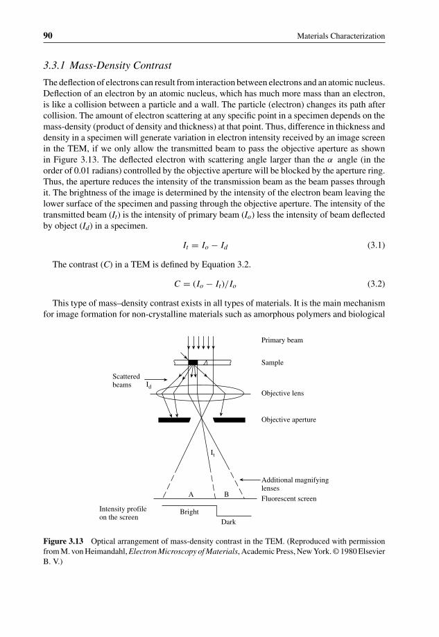
3.3.1 Mass-Density Contrast
The deflection of electrons can result from interaction between electrons and an atomic nucleus.Deflection of an electron by an atomic nucleus, which has much more mass than an electron,is like a collision between a particle and a wall. The particle (electron) changes its path aftercollision. The amount of electron scattering at any specific point in a specimen depends on themass-density (product of density and thickness) at that point. Thus, difference in thickness anddensity in a specimen will generate variation in electron intensity received by an image screenin the TEM, if we only allow the transmitted beam to pass the objective aperture as shownin Figure 3.13. The deflected electron with scattering angle larger than the α angle (in theorder of 0.01 radians) controlled by the objective aperture will be blocked by the aperture ring.Thus, the aperture reduces the intensity of the transmission beam as the beam passes throughit. The brightness of the image is determined by the intensity of the electron beam leaving thelower surface of the specimen and passing through the objective aperture. The intensity of thetransmitted beam (It) is the intensity of primary beam (Io) less the intensity of beam deflectedby object (Id) in a specimen.
It = Io − Id (3.1)
The contrast (C) in a TEM is defined by Equation 3.2.
C = (Io − It)/Io (3.2)
This type of mass–density contrast exists in all types of materials. It is the main mechanismfor image formation for non-crystalline materials such as amorphous polymers and biological
Primary beam
Sample
Objective lens
Objective aperture
Additional magnifyinglenses
Fluorescent screenA B
BrightDark
Intensity profileon the screen
Scatteredbeams
It
Id
Figure 3.13 Optical arrangement of mass-density contrast in the TEM. (Reproduced with permissionfrom M. von Heimandahl, Electron Microscopy of Materials, Academic Press, New York. © 1980 ElsevierB. V.)

Transmission Electron Microscopy 91
specimens. The mass-density contrast is also described as ‘absorption contrast’, which is rathermisleading because there is little electron absorption by the specimen.
In order to increase contrast, polymeric and biological specimens often are stained by solu-tions containing high density substances such as heavy metal oxides. The ions of metal oxidesin solution selectively penetrate certain constituents of the microstructure, and thus increaseits mass-density. Figure 3.14 is an example of a TEM image showing mass-density contrast ina specimen of polymer blend containing polycarbonate (PC) and polybutylene terephthalate(PBT). The PC phase appears darker because it is rich in staining substance, RuO4. Besidesstaining, common effective techniques to increase contrast include using a smaller objectiveaperture and using a lower acceleration voltage. The negative side of using such techniques isreduction of total brightness.
Figure 3.14 TEM image of PC–PBT polymer blends with mass-density contrast. The specimen isstained with RuO4. (Reproduced with permission of Jingshen Wu.)

92 Materials Characterization
3.3.2 Diffraction Contrast
We can also generate contrast in the TEM by a diffraction method. Diffraction contrast isthe primary mechanism of TEM image formation in crystalline specimens. Diffraction canbe regarded as collective deflection of electrons. Electrons can be scattered collaborativelyby parallel crystal planes similar to X-rays. Bragg’s Law (Equation 2.1), which applies toX-ray diffraction, also applies to electron diffraction. When the Bragg conditions are satis-fied at certain angles between electron beams and crystal orientation, constructive diffractionoccurs and strong electron deflection in a specimen results, as schematically illustrated inFigure 3.15. Thus, the intensity of the transmitted beam is reduced when the objective aperture
Figure 3.15 Electron deflection by Bragg diffraction of a crystalline specimen: (a) image formationin crystalline samples; and (b) diffraction at crystal lattice planes and at the contours of inclusions.(Reproduced with permission from M. von Heimandahl, Electron Microscopy of Materials, AcademicPress, New York. © 1980 Elsevier B. V.)
Transmission Electron Microscopy 93
blocks the diffraction beams, similar to the situation of mass-density contrast. Note that themain difference between the two contrasts is that the diffraction contrast is very sensitive tospecimen tilting in the specimen holder but mass-density contrast is only sensitive to total massin thickness per surface area.
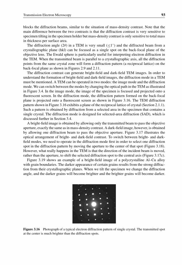
The diffraction angle (2θ) in a TEM is very small (≤1◦) and the diffracted beam from acrystallographic plane (hkl) can be focused as a single spot on the back-focal plane of theobjective lens. The Ewald sphere is particularly useful for interpreting electron diffraction inthe TEM. When the transmitted beam is parallel to a crystallographic axis, all the diffractionpoints from the same crystal zone will form a diffraction pattern (a reciprocal lattice) on theback-focal plane as shown in Figures 2.9 and 2.11.
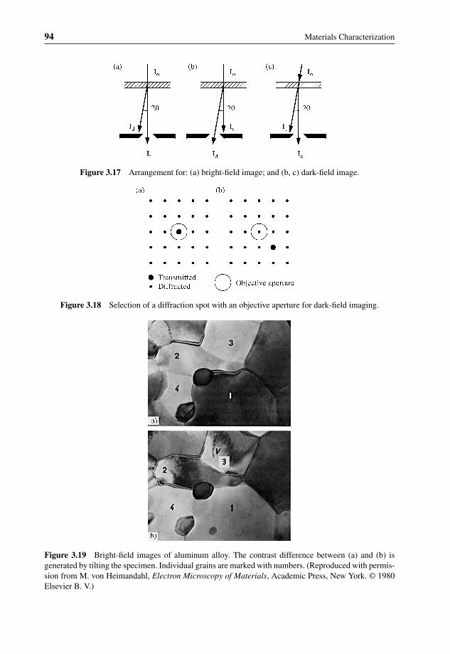
The diffraction contrast can generate bright-field and dark-field TEM images. In order tounderstand the formation of bright-field and dark-field images, the diffraction mode in a TEMmust be mentioned. A TEM can be operated in two modes: the image mode and the diffractionmode. We can switch between the modes by changing the optical path in the TEM as illustratedin Figure 3.4. In the image mode, the image of the specimen is focused and projected onto afluorescent screen. In the diffraction mode, the diffraction pattern formed on the back-focalplane is projected onto a fluorescent screen as shown in Figure 3.16. The TEM diffractionpattern shown in Figure 3.16 exhibits a plane of the reciprocal lattice of crystal (Section 2.1.1).Such a pattern is obtained by diffraction from a selected area in the specimen that contains asingle crystal. The diffraction mode is designed for selected-area diffraction (SAD), which isdiscussed further in Section 3.4.
A bright-field image is obtained by allowing only the transmitted beam to pass the objectiveaperture, exactly the same as in mass-density contrast. A dark-field image, however, is obtainedby allowing one diffraction beam to pass the objective aperture. Figure 3.17 illustrates theoptical arrangement of bright- and dark-field contrast. To switch between bright- and dark-field modes, we need to operate in the diffraction mode first in order to select one diffractionspot in the diffraction pattern by moving the aperture to the center of that spot (Figure 3.18).However, what really happens in the TEM is that the direction of the incident beam is moved,rather than the aperture, to shift the selected diffraction spot to the central axis (Figure 3.17c).
Figure 3.19 shows an example of a bright-field image of a polycrystalline Al–Cu alloywith grain boundaries. The darker appearance of certain grains results from the strong diffrac-tion from their crystallographic planes. When we tilt the specimen we change the diffractionangle, and the darker grains will become brighter and the brighter grains will become darker.
Figure 3.16 Photograph of a typical electron diffraction pattern of single crystal. The transmitted spotat the center is much brighter than the diffraction spots.
94 Materials Characterization
Figure 3.17 Arrangement for: (a) bright-field image; and (b, c) dark-field image.
Figure 3.18 Selection of a diffraction spot with an objective aperture for dark-field imaging.
Figure 3.19 Bright-field images of aluminum alloy. The contrast difference between (a) and (b) isgenerated by tilting the specimen. Individual grains are marked with numbers. (Reproduced with permis-sion from M. von Heimandahl, Electron Microscopy of Materials, Academic Press, New York. © 1980Elsevier B. V.)
Transmission Electron Microscopy 95
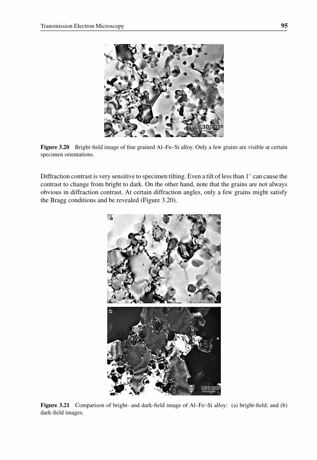
Figure 3.20 Bright-field image of fine grained Al–Fe–Si alloy. Only a few grains are visible at certainspecimen orientations.
Diffraction contrast is very sensitive to specimen tilting. Even a tilt of less than 1◦ can cause thecontrast to change from bright to dark. On the other hand, note that the grains are not alwaysobvious in diffraction contrast. At certain diffraction angles, only a few grains might satisfythe Bragg conditions and be revealed (Figure 3.20).
Figure 3.21 Comparison of bright- and dark-field image of Al–Fe–Si alloy: (a) bright-field; and (b)dark-field images.

96 Materials Characterization
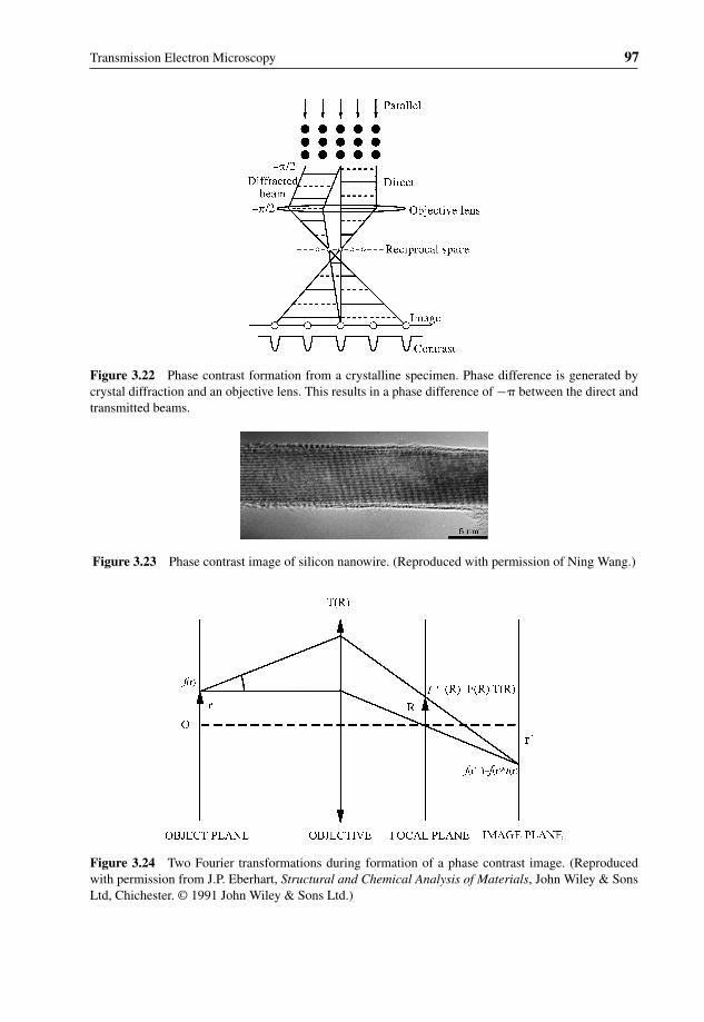
Dark-field is not as commonly used as bright-field imaging. However, the dark-field imagemay reveal more fine features that are bright when the background becomes dark. Figure 3.21shows a comparison between bright- and dark-field images for the same area in an Al–Fe–Sialloy. The dark-field image (Figure 3.21b) reveals finer details inside the grains. Interestingly,there are several dark-field images corresponding to a single bright-field image because wecan select different diffraction spots (hkl) in Figure 3.18 to obtain a dark-field image. This isdifferent from light microscopy in which there is a one-to-one correlation between bright- anddark-field images. When tilting a specimen to generate a high intensity diffraction spot (hkl),we may chose the spot of (
—hkl), which must exhibit low intensity in this circumstance, to form
a dark-field image. This type of dark-field image is called the weak-beam dark-field image.Weak-beam imaging is useful for increasing the resolution of fine features such as dislocationsin crystalline materials.
3.3.3 Phase Contrast
Both mass-density and diffraction contrasts are amplitude contrast because they use onlythe amplitude change of transmitted electron waves. Chapter 1 mentions that phase changegenerates contrast in light microscopy. Similarly, a TEM can also use phase difference inelectron waves to generate contrast. The phase contrast mechanism, however, is much morecomplicated than that of light microscopy. The TEM phase contrast produces the highestresolution of lattice and structure images for crystalline materials. Thus, phase contrast isoften referred as to high resolution transmission electron microscopy (HRTEM).
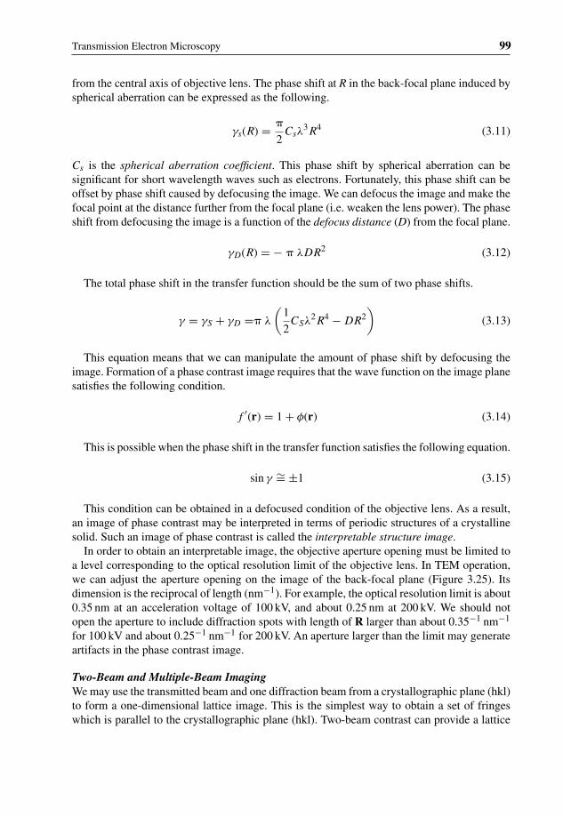
Phase contrast must involve at least two electron waves that are different in wave phase.Thus, we should allow at least two beams (the transmitted beam and a diffraction beam) toparticipate in image formation in a TEM. Formation of phase contrast in a crystalline specimenis illustrated simply in Figure 3.22. A crystalline specimen with a periodic lattice structuregenerates a phase difference between the transmitted and diffracted beams. The objective lensgenerates additional phase difference among the beams. Recombination of transmitted anddiffracted beams will generate an interference pattern with periodic dark–bright changes onthe image plane because of beam interferences, as shown in Figure 3.23. An interferencepattern is a fringe type that reveals the periodic nature of a crystal.
Theoretical interpretation of phase contrast images is complicated, particularly when morethan one diffraction spot participates in image formation. The schematic illustration inFigure 3.22 does not reflect the complexity of phase contrast. The electron wave theory ofphase contrast formation is explained briefly in the following section.
Theoretical AspectsThe electron wave path of phase contrast in a TEM is illustrated by Figure 3.24. The propertiesof electron waves exiting the specimen are represented by an object function, f(r), whichincludes the distributions of wave amplitude and phase. r is the position vector from thecentral optical axis. The object function may be represented as a function in Equation 3.3.
f (r) = [1 − s(r)] exp [iφ(r)] (3.3)
Transmission Electron Microscopy 97
Figure 3.22 Phase contrast formation from a crystalline specimen. Phase difference is generated bycrystal diffraction and an objective lens. This results in a phase difference of −� between the direct andtransmitted beams.
Figure 3.23 Phase contrast image of silicon nanowire. (Reproduced with permission of Ning Wang.)
Figure 3.24 Two Fourier transformations during formation of a phase contrast image. (Reproducedwith permission from J.P. Eberhart, Structural and Chemical Analysis of Materials, John Wiley & SonsLtd, Chichester. © 1991 John Wiley & Sons Ltd.)

98 Materials Characterization
where s(r) represents absorption by the specimen and φ(r) is a phase component of a wave.For a weakly scattering object (s and φ � 1), f(r) may be approximated.
f (r) = 1 − s(r) + iφ(r) (3.4)
At the back-focal plane of objective lens, the diffraction pattern is considered as the Fouriertransform (FT) of the object function.
F (R) = FTf (r) (3.5)
where R is the position vector of a diffraction spot from the central axis on the focal plane; areciprocal vector. The Fourier transform F(R) is defined by the following equation.
F (R) =∫
∞f (r)exp(2 � ir • R)dr3 (3.6)
in which r•R is defined.
r • R = xX + yY + zY (3.7)
X, Y and Z are the magnitudes of reciprocal vector R, corresponding to the magnitude (x,y and z) of vector r in the real space. Since the electron waves pass the objective lens, theobjective lens can affect the wave characteristics. The effect of the objective lens on the wavefunction can be represented by a transfer function, T(R). Thus, the actual wave function on theback-focal plane becomes the following function.
F ′(R) = F (R)T (R) (3.8)
Wave theory tells us that the wave function of electrons on the image plane (florescentscreen) should be the Fourier transform of F′(R). For treatment simplicity, we may ignore theimage magnification and rotation on the image plane. Then, the wave function on the imageplane becomes f ′(r).
f ′(r) = FT {F ′(R)} = FT {F (R)T (R)} = f (r)∗t(r) (3.9)
The results should be read as the convolution product of f(r) by t(r), where t(r) is the Fouriertransform of T(R). The transfer function plays an important role in image formation. Thetransfer function can be written as the following equation.
T (R) = A(R)exp[−iγ(R)] (3.10)
where the amplitude factor (A) equals unity when the length of R is less than the objectiveaperture radius on the focal plane; otherwise it equals zero. The phase shift (γ) that occurs asthe waves pass objective lens should be considered. Phase difference occurs when the wavepaths that reach a certain point are different. Spherical aberration causes phase shift becauseof the electron wave path difference between the waves near the central axis and the waves far
Transmission Electron Microscopy 99
from the central axis of objective lens. The phase shift at R in the back-focal plane induced byspherical aberration can be expressed as the following.
γs(R) = �
2Csλ
3R4 (3.11)
Cs is the spherical aberration coefficient. This phase shift by spherical aberration can besignificant for short wavelength waves such as electrons. Fortunately, this phase shift can beoffset by phase shift caused by defocusing the image. We can defocus the image and make thefocal point at the distance further from the focal plane (i.e. weaken the lens power). The phaseshift from defocusing the image is a function of the defocus distance (D) from the focal plane.
γD(R) = − � λDR2 (3.12)
The total phase shift in the transfer function should be the sum of two phase shifts.
γ = γS + γD =� λ
(1
2CSλ2R4 − DR2
)(3.13)
This equation means that we can manipulate the amount of phase shift by defocusing theimage. Formation of a phase contrast image requires that the wave function on the image planesatisfies the following condition.
f ′(r) = 1 + φ(r) (3.14)
This is possible when the phase shift in the transfer function satisfies the following equation.
sin γ ∼= ±1 (3.15)
This condition can be obtained in a defocused condition of the objective lens. As a result,an image of phase contrast may be interpreted in terms of periodic structures of a crystallinesolid. Such an image of phase contrast is called the interpretable structure image.
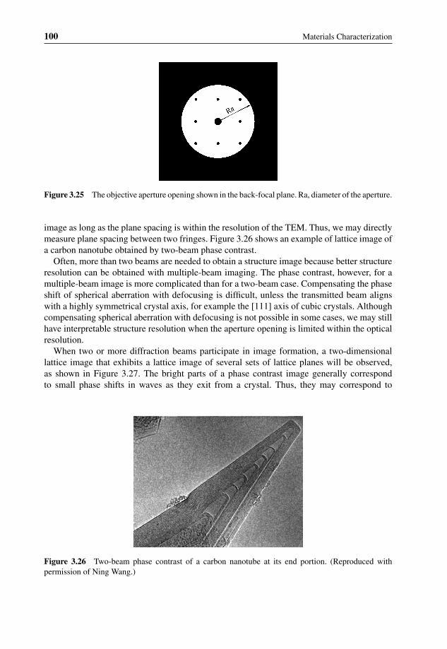
In order to obtain an interpretable image, the objective aperture opening must be limited toa level corresponding to the optical resolution limit of the objective lens. In TEM operation,we can adjust the aperture opening on the image of the back-focal plane (Figure 3.25). Itsdimension is the reciprocal of length (nm−1). For example, the optical resolution limit is about0.35 nm at an acceleration voltage of 100 kV, and about 0.25 nm at 200 kV. We should notopen the aperture to include diffraction spots with length of R larger than about 0.35−1 nm−1
for 100 kV and about 0.25−1 nm−1 for 200 kV. An aperture larger than the limit may generateartifacts in the phase contrast image.
Two-Beam and Multiple-Beam ImagingWe may use the transmitted beam and one diffraction beam from a crystallographic plane (hkl)to form a one-dimensional lattice image. This is the simplest way to obtain a set of fringeswhich is parallel to the crystallographic plane (hkl). Two-beam contrast can provide a lattice
100 Materials Characterization
Figure 3.25 The objective aperture opening shown in the back-focal plane. Ra, diameter of the aperture.
image as long as the plane spacing is within the resolution of the TEM. Thus, we may directlymeasure plane spacing between two fringes. Figure 3.26 shows an example of lattice image ofa carbon nanotube obtained by two-beam phase contrast.
Often, more than two beams are needed to obtain a structure image because better structureresolution can be obtained with multiple-beam imaging. The phase contrast, however, for amultiple-beam image is more complicated than for a two-beam case. Compensating the phaseshift of spherical aberration with defocusing is difficult, unless the transmitted beam alignswith a highly symmetrical crystal axis, for example the [111] axis of cubic crystals. Althoughcompensating spherical aberration with defocusing is not possible in some cases, we may stillhave interpretable structure resolution when the aperture opening is limited within the opticalresolution.
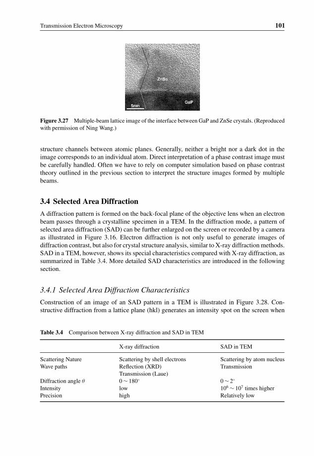
When two or more diffraction beams participate in image formation, a two-dimensionallattice image that exhibits a lattice image of several sets of lattice planes will be observed,as shown in Figure 3.27. The bright parts of a phase contrast image generally correspondto small phase shifts in waves as they exit from a crystal. Thus, they may correspond to
Figure 3.26 Two-beam phase contrast of a carbon nanotube at its end portion. (Reproduced withpermission of Ning Wang.)
Transmission Electron Microscopy 101
Figure 3.27 Multiple-beam lattice image of the interface between GaP and ZnSe crystals. (Reproducedwith permission of Ning Wang.)
structure channels between atomic planes. Generally, neither a bright nor a dark dot in theimage corresponds to an individual atom. Direct interpretation of a phase contrast image mustbe carefully handled. Often we have to rely on computer simulation based on phase contrasttheory outlined in the previous section to interpret the structure images formed by multiplebeams.
3.4 Selected Area Diffraction
A diffraction pattern is formed on the back-focal plane of the objective lens when an electronbeam passes through a crystalline specimen in a TEM. In the diffraction mode, a pattern ofselected area diffraction (SAD) can be further enlarged on the screen or recorded by a cameraas illustrated in Figure 3.16. Electron diffraction is not only useful to generate images ofdiffraction contrast, but also for crystal structure analysis, similar to X-ray diffraction methods.SAD in a TEM, however, shows its special characteristics compared with X-ray diffraction, assummarized in Table 3.4. More detailed SAD characteristics are introduced in the followingsection.
3.4.1 Selected Area Diffraction Characteristics
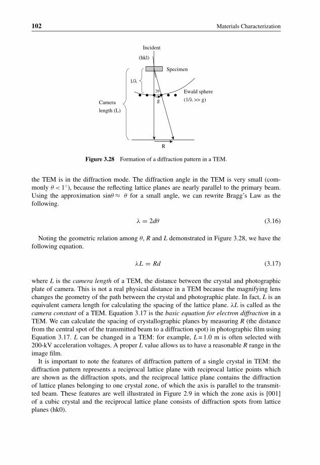
Construction of an image of an SAD pattern in a TEM is illustrated in Figure 3.28. Con-structive diffraction from a lattice plane (hkl) generates an intensity spot on the screen when
Table 3.4 Comparison between X-ray diffraction and SAD in TEM
X-ray diffraction SAD in TEM
Scattering Nature Scattering by shell electrons Scattering by atom nucleusWave paths Reflection (XRD) Transmission
Transmission (Laue)Diffraction angle θ 0 ∼ 180◦ 0 ∼ 2◦
Intensity low 106 ∼ 107 times higherPrecision high Relatively low
102 Materials Characterization
Camera
length (L)
Incident
(hkl)
Specimen
Ewald sphere
(1/λ >> g)
1/λ
g
R
2θ
Figure 3.28 Formation of a diffraction pattern in a TEM.
the TEM is in the diffraction mode. The diffraction angle in the TEM is very small (com-monly θ < 1◦), because the reflecting lattice planes are nearly parallel to the primary beam.Using the approximation sinθ ≈ θ for a small angle, we can rewrite Bragg’s Law as thefollowing.
λ = 2dθ (3.16)
Noting the geometric relation among θ, R and L demonstrated in Figure 3.28, we have thefollowing equation.
λL = Rd (3.17)
where L is the camera length of a TEM, the distance between the crystal and photographicplate of camera. This is not a real physical distance in a TEM because the magnifying lenschanges the geometry of the path between the crystal and photographic plate. In fact, L is anequivalent camera length for calculating the spacing of the lattice plane. λL is called as thecamera constant of a TEM. Equation 3.17 is the basic equation for electron diffraction in aTEM. We can calculate the spacing of crystallographic planes by measuring R (the distancefrom the central spot of the transmitted beam to a diffraction spot) in photographic film usingEquation 3.17. L can be changed in a TEM: for example, L = 1.0 m is often selected with200-kV acceleration voltages. A proper L value allows us to have a reasonable R range in theimage film.
It is important to note the features of diffraction pattern of a single crystal in TEM: thediffraction pattern represents a reciprocal lattice plane with reciprocal lattice points whichare shown as the diffraction spots, and the reciprocal lattice plane contains the diffractionof lattice planes belonging to one crystal zone, of which the axis is parallel to the transmit-ted beam. These features are well illustrated in Figure 2.9 in which the zone axis is [001]of a cubic crystal and the reciprocal lattice plane consists of diffraction spots from latticeplanes (hk0).

Transmission Electron Microscopy 103
Figure 3.29 Diffraction pattern formation from a thin foil specimen in a TEM. The surface of Ewaldsphere intersects the elongated diffraction spots. An elongated spot reflects the diffraction intensitydistribution along the transmitted beam direction.
The Ewald sphere is very useful to explain the formation of diffraction patterns in a TEM(Figure 2.11). Recall that the short wavelength of high energy electrons makes the radius ofthe Ewald sphere (λ−1) become so large that the spherical surface is nearly flat comparedwith the distances between reciprocal lattice points. On the other hand, a diffraction spot of acrystal with a small dimension in the vertical direction is not an exact reciprocal lattice point,but an elongated spot along that direction, as illustrated in Figure 3.29. The reason for spotelongation relates to diffraction intensity distribution, which can be fully explained by kine-matic diffraction theory. Without more description of the theory, we may still understand it byrecalling the discussion of crystal size effects on width of X-ray diffraction (XRD) diffractionpeaks in Chapter 2. The width of XRD peaks increases with decreasing crystal size because asmall crystal causes incomplete destructive interference. For the same reason, the thin crystalof a TEM specimen causes a widened intensity distribution and thus, the elongated diffrac-tion spots along the vertical direction. Therefore, the flat surface of the large Ewald spherecan intersect even more diffraction spots on one reciprocal plane in a TEM as illustrated inFigure 3.29. Thus, we can see a diffraction pattern in the TEM as shown in Figure 3.16.
3.4.2 Single-Crystal Diffraction
To obtain a diffraction pattern as shown in Figure 3.16, we need to use the selected areaaperture to isolate a single crystal in the image mode, and then switch to the diffraction mode.Commonly, tilting the specimen is necessary to obtain a diffraction pattern with high symmetrywith respect to its central transmitted spot. A symmetrical pattern like Figure 3.16 must have azone axis of the crystal aligned with the transmitted beam direction, as illustrated in Figure 2.9.
After obtaining a diffraction pattern, we may want to index the pattern in order to knowthe crystal structure or crystal orientation that the pattern represents. Indexing a pattern meansto assign a set of h, k and l to each diffraction spot in the pattern. The information can bedirectly extracted from a pattern that includes the length of R for each spot and angles betweenany two R vectors. We can calculate the interplanar spacing (dhkl) easily using Equation 3.17,with knowledge of the camera constant. Without additional information about the crystal suchas chemical composition or lattice parameters, indexing a pattern could be a difficult task.However, indexing techniques for simple cases can be demonstrated as follows.

104 Materials Characterization
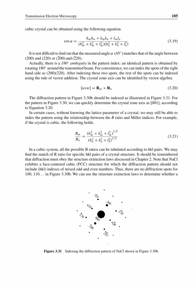
Figure 3.30 Single crystal of NaCl: (a) bright-field image; and (b) selected area diffraction pattern.Rm, Rn are the radii of spots m and n, respectively. The transmitted beam direction is parallel to [001].
Indexing a Cubic Crystal PatternThe TEM bright-field image and an SAD pattern of sodium chloride (NaCl) are shown inFigure 3.30. In the pattern, the central spot of the transmitted beam is brightest and should beindexed as (0 0 0) of the reciprocal lattice plane. Then, we can select two spots, for example mand n in the pattern to measure their R lengths and angle between them. Here, the R lengths ofm and n are measured as 8.92 mm and 12.6 mm, respectively; and the angle between Rm andRn is measured as 45◦. The indices of the spots can be determined by the following relationshipfor cubic crystals such as NaCl. The equation is obtained by combining Equation 3.17 andEquation 2.4.
R(hkl) = λL(h2 + k2 + l2)1/2
a(3.18)
The wavelength of electrons (λ) for 200 kV, which is used to obtain the pattern, should be0.00251 nm according to Table 3.2. The diffraction photograph is taken at the camera length(L) of 1.0 m. Since the lattice parameter of NaCl (a) is 0.563 nm, we can find out that the Rmmatches that of 200 and Rn matches that of 220, according Equation 3.18. Then, we shouldcheck whether the angle (RmRn) matches that between specific planes. The plane angle in a
Transmission Electron Microscopy 105
cubic crystal can be obtained using the following equation.
cos α = hmhn + kmkn + lmln
(h2m + k2
m + l2m)(h2n + k2
n + l2n)(3.19)
It is not difficult to find out that the measured angle α (45◦) matches that of the angle between(200) and (220) or (2̄00) and (2̄20).
Actually, there is a 180◦ ambiguity in the pattern index: an identical pattern is obtained byrotating 180◦ around the transmitted beam. For convenience, we can index the spots of the righthand side as (200)(220). After indexing these two spots, the rest of the spots can be indexedusing the rule of vector addition. The crystal zone axis can be identified by vector algebra.
[uvw] = Rm × Rn (3.20)
The diffraction pattern in Figure 3.30b should be indexed as illustrated in Figure 3.31. Forthe pattern in Figure 3.30, we can quickly determine the crystal zone axis as [001], accordingto Equation 3.20.
In certain cases, without knowing the lattice parameter of a crystal, we may still be able toindex the pattern using the relationship between the R ratio and Miller indices. For example,if the crystal is cubic, the following holds.
Rm
Rn
= (h2m + k2
m + l2m)1/2
(h2n + k2
n + l2n)1/2 (3.21)
In a cubic system, all the possible R ratios can be tabulated according to hkl pairs. We mayfind the match of R ratio for specific hkl pairs of a crystal structure. It should be rememberedthat diffraction must obey the structure extinction laws discussed in Chapter 2. Note that NaClexhibits a face-centered cubic (FCC) structure for which the diffraction pattern should notinclude (hkl) indexes of mixed odd and even numbers. Thus, there are no diffraction spots for100, 110. . . in Figure 3.30b. We can use the structure extinction laws to determine whether a
Figure 3.31 Indexing the diffraction pattern of NaCl shown in Figure 3.30b.
106 Materials Characterization
Table 3.5 Relationship between Real and Reciprocal Lattice Structure
Real lattice Reciprocal Reciprocal latticeReal lattice parameter lattice parameter
Simple cubic a Simple cubic a∗ = 1a
FCC a BCC a∗ = 2a
BCC a FCC a∗ = 2a
cubic crystal is FCC or body-centered cubic (BCC). According the structure extinction lawslisted in Table 2.2, the reciprocal lattice of an FCC structure is a BCC type or vice-versa, asshown in Table 3.5.
The crystal orientation with respect to specimen geometry is important information. InFigure 3.30, the NaCl crystal orientation is already revealed by its bright field image, becauseits cubic shape implies its crystal structure and orientation. In most cases, crystalline materialsdo not show the geometrical shape representing their crystal structure and orientation. Thus,we need to determine the orientation from single-crystal diffraction patterns.
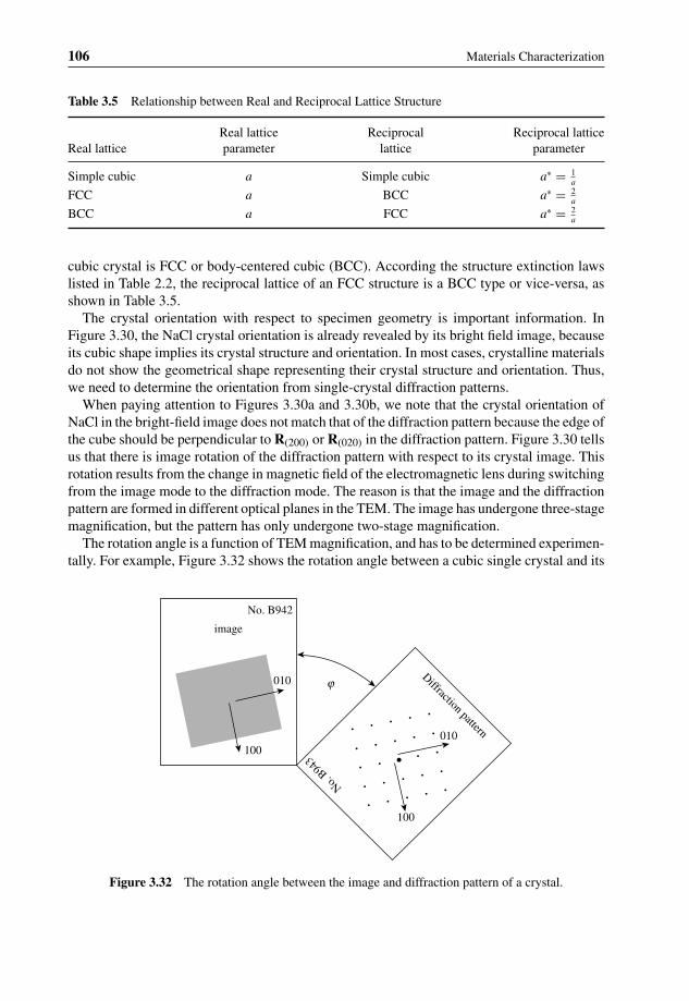
When paying attention to Figures 3.30a and 3.30b, we note that the crystal orientation ofNaCl in the bright-field image does not match that of the diffraction pattern because the edge ofthe cube should be perpendicular to R(200) or R(020) in the diffraction pattern. Figure 3.30 tellsus that there is image rotation of the diffraction pattern with respect to its crystal image. Thisrotation results from the change in magnetic field of the electromagnetic lens during switchingfrom the image mode to the diffraction mode. The reason is that the image and the diffractionpattern are formed in different optical planes in the TEM. The image has undergone three-stagemagnification, but the pattern has only undergone two-stage magnification.
The rotation angle is a function of TEM magnification, and has to be determined experimen-tally. For example, Figure 3.32 shows the rotation angle between a cubic single crystal and its
No. B942
image
010
100010
100
Diffraction pattern
No. B94
3
j
Figure 3.32 The rotation angle between the image and diffraction pattern of a crystal.
Transmission Electron Microscopy 107
diffraction pattern. Note that the angle is ϕ + 180◦, not ϕ, because each stage of magnificationrotates the image by 180◦. After calibrating the rotation angle at the given acceleration volt-age, magnification and camera length, we should be able to determine the orientation of thecrystal being examined. Some modern TEM systems have a function to correct the angle ofimage rotation automatically. Thus, manual correction is no longer needed when the imagesare recorded.
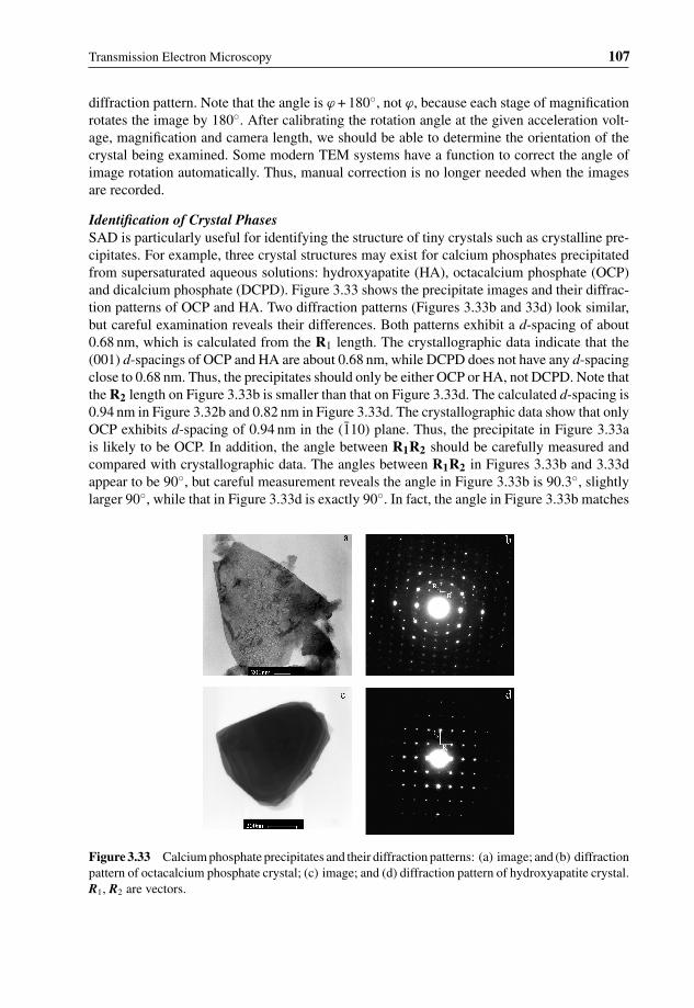
Identification of Crystal PhasesSAD is particularly useful for identifying the structure of tiny crystals such as crystalline pre-cipitates. For example, three crystal structures may exist for calcium phosphates precipitatedfrom supersaturated aqueous solutions: hydroxyapatite (HA), octacalcium phosphate (OCP)and dicalcium phosphate (DCPD). Figure 3.33 shows the precipitate images and their diffrac-tion patterns of OCP and HA. Two diffraction patterns (Figures 3.33b and 33d) look similar,but careful examination reveals their differences. Both patterns exhibit a d-spacing of about0.68 nm, which is calculated from the R1 length. The crystallographic data indicate that the(001) d-spacings of OCP and HA are about 0.68 nm, while DCPD does not have any d-spacingclose to 0.68 nm. Thus, the precipitates should only be either OCP or HA, not DCPD. Note thatthe R2 length on Figure 3.33b is smaller than that on Figure 3.33d. The calculated d-spacing is0.94 nm in Figure 3.32b and 0.82 nm in Figure 3.33d. The crystallographic data show that onlyOCP exhibits d-spacing of 0.94 nm in the (1̄10) plane. Thus, the precipitate in Figure 3.33ais likely to be OCP. In addition, the angle between R1R2 should be carefully measured andcompared with crystallographic data. The angles between R1R2 in Figures 3.33b and 3.33dappear to be 90◦, but careful measurement reveals the angle in Figure 3.33b is 90.3◦, slightlylarger 90◦, while that in Figure 3.33d is exactly 90◦. In fact, the angle in Figure 3.33b matches
Figure 3.33 Calcium phosphate precipitates and their diffraction patterns: (a) image; and (b) diffractionpattern of octacalcium phosphate crystal; (c) image; and (d) diffraction pattern of hydroxyapatite crystal.R1, R2 are vectors.
108 Materials Characterization
the crystallographic data of OCP, because the planar angle between OCP (001) and (1̄10) is90.318◦. Thus, we can confidently identify the crystal structure of the precipitate in Figure3.33a as OCP, which has a triclinic structure, while the precipitate in Figure 3.33c is identifiedas HA with a hexagonal structure.
3.4.3 Multi-Crystal Diffraction
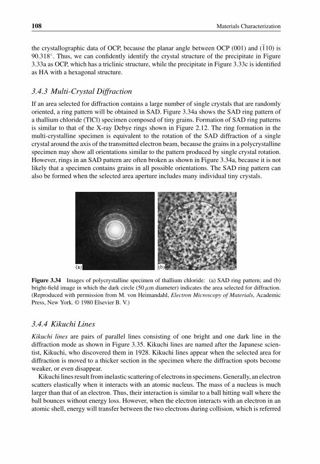
If an area selected for diffraction contains a large number of single crystals that are randomlyoriented, a ring pattern will be obtained in SAD. Figure 3.34a shows the SAD ring pattern ofa thallium chloride (TlCl) specimen composed of tiny grains. Formation of SAD ring patternsis similar to that of the X-ray Debye rings shown in Figure 2.12. The ring formation in themulti-crystalline specimen is equivalent to the rotation of the SAD diffraction of a singlecrystal around the axis of the transmitted electron beam, because the grains in a polycrystallinespecimen may show all orientations similar to the pattern produced by single crystal rotation.However, rings in an SAD pattern are often broken as shown in Figure 3.34a, because it is notlikely that a specimen contains grains in all possible orientations. The SAD ring pattern canalso be formed when the selected area aperture includes many individual tiny crystals.
Figure 3.34 Images of polycrystalline specimen of thallium chloride: (a) SAD ring pattern; and (b)bright-field image in which the dark circle (50 µm diameter) indicates the area selected for diffraction.(Reproduced with permission from M. von Heimandahl, Electron Microscopy of Materials, AcademicPress, New York. © 1980 Elsevier B. V.)
3.4.4 Kikuchi Lines
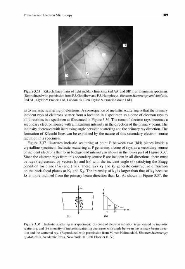
Kikuchi lines are pairs of parallel lines consisting of one bright and one dark line in thediffraction mode as shown in Figure 3.35. Kikuchi lines are named after the Japanese scien-tist, Kikuchi, who discovered them in 1928. Kikuchi lines appear when the selected area fordiffraction is moved to a thicker section in the specimen where the diffraction spots becomeweaker, or even disappear.
Kikuchi lines result from inelastic scattering of electrons in specimens. Generally, an electronscatters elastically when it interacts with an atomic nucleus. The mass of a nucleus is muchlarger than that of an electron. Thus, their interaction is similar to a ball hitting wall where theball bounces without energy loss. However, when the electron interacts with an electron in anatomic shell, energy will transfer between the two electrons during collision, which is referred
Transmission Electron Microscopy 109
Figure 3.35 Kikuchi lines (pairs of light and dark lines) marked AA′ and BB′ in an aluminum specimen.(Reproduced with permission from P.J. Goodhew and F.J. Humphreys, Electron Microscopy and Analysis,2nd ed., Taylor & Francis Ltd, London. © 1988 Taylor & Francis Group Ltd.)
as to inelastic scattering of electrons. A consequence of inelastic scattering is that the primaryincident rays of electrons scatter from a location in a specimen as a cone of electron rays toall directions in a specimen as illustrated in Figure 3.36. The cone of electron rays becomes asecondary electron source with a maximum intensity in the direction of the primary beam. Theintensity decreases with increasing angle between scattering and the primary ray direction. Theformation of Kikuchi lines can be explained by the nature of this secondary electron sourceradiation in a specimen.
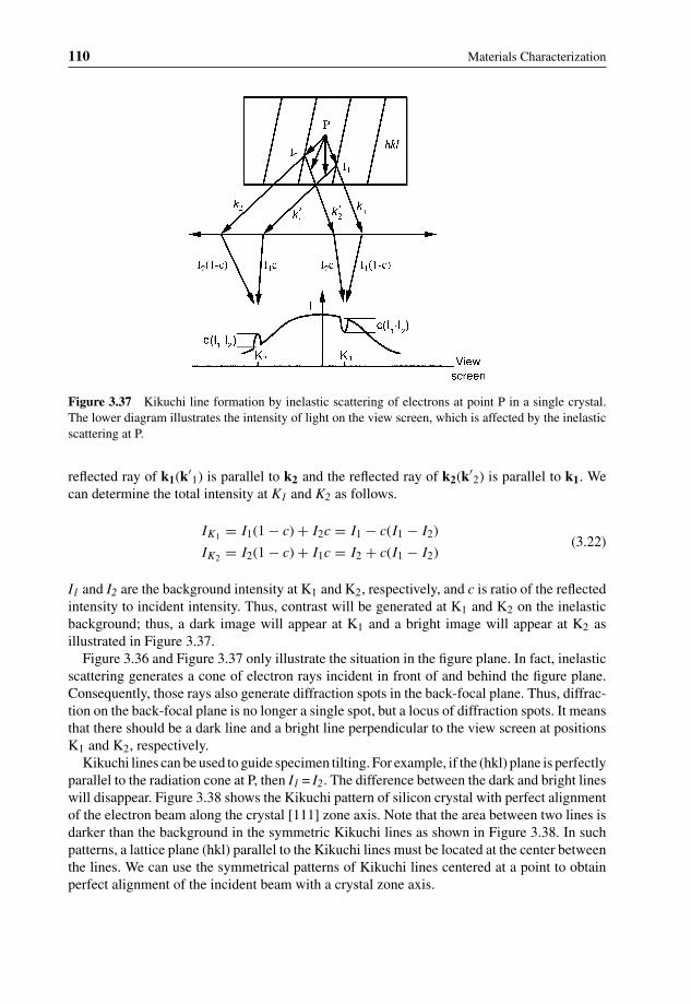
Figure 3.37 illustrates inelastic scattering at point P between two (hkl) planes inside acrystalline specimen. Inelastic scattering at P generates a cone of rays as a secondary sourceof incident electrons that form background intensity as shown in the lower part of Figure 3.37.Since the electron rays from this secondary source P are incident in all directions, there mustbe rays (represented by vectors k1 and k2) with the incident angle (θ) satisfying the Braggcondition for plane (hkl) and (
—hkl). These rays k1 and k2 generate constructive diffraction
on the back-focal planes at K1 and K2. The intensity of k1 is larger than that of k2 becausek2 is more inclined from the primary beam direction than k1. As shown in Figure 3.37, the
aa
aIa
Ibb
b
I
IIo
(a) (b)
Figure 3.36 Inelastic scattering in a specimen: (a) cone of electron radiation is generated by inelasticscattering; and (b) intensity of inelastic scattering decreases with angle between the primary beam direc-tion and the scattered ray. (Reproduced with permission from M. von Heimandahl, Electron Microscopyof Materials, Academic Press, New York. © 1980 Elsevier B. V.)
110 Materials Characterization
Figure 3.37 Kikuchi line formation by inelastic scattering of electrons at point P in a single crystal.The lower diagram illustrates the intensity of light on the view screen, which is affected by the inelasticscattering at P.
reflected ray of k1(k′1) is parallel to k2 and the reflected ray of k2(k′
2) is parallel to k1. Wecan determine the total intensity at K1 and K2 as follows.
IK1 = I1(1 − c) + I2c = I1 − c(I1 − I2)
IK2 = I2(1 − c) + I1c = I2 + c(I1 − I2)(3.22)
I1 and I2 are the background intensity at K1 and K2, respectively, and c is ratio of the reflectedintensity to incident intensity. Thus, contrast will be generated at K1 and K2 on the inelasticbackground; thus, a dark image will appear at K1 and a bright image will appear at K2 asillustrated in Figure 3.37.
Figure 3.36 and Figure 3.37 only illustrate the situation in the figure plane. In fact, inelasticscattering generates a cone of electron rays incident in front of and behind the figure plane.Consequently, those rays also generate diffraction spots in the back-focal plane. Thus, diffrac-tion on the back-focal plane is no longer a single spot, but a locus of diffraction spots. It meansthat there should be a dark line and a bright line perpendicular to the view screen at positionsK1 and K2, respectively.
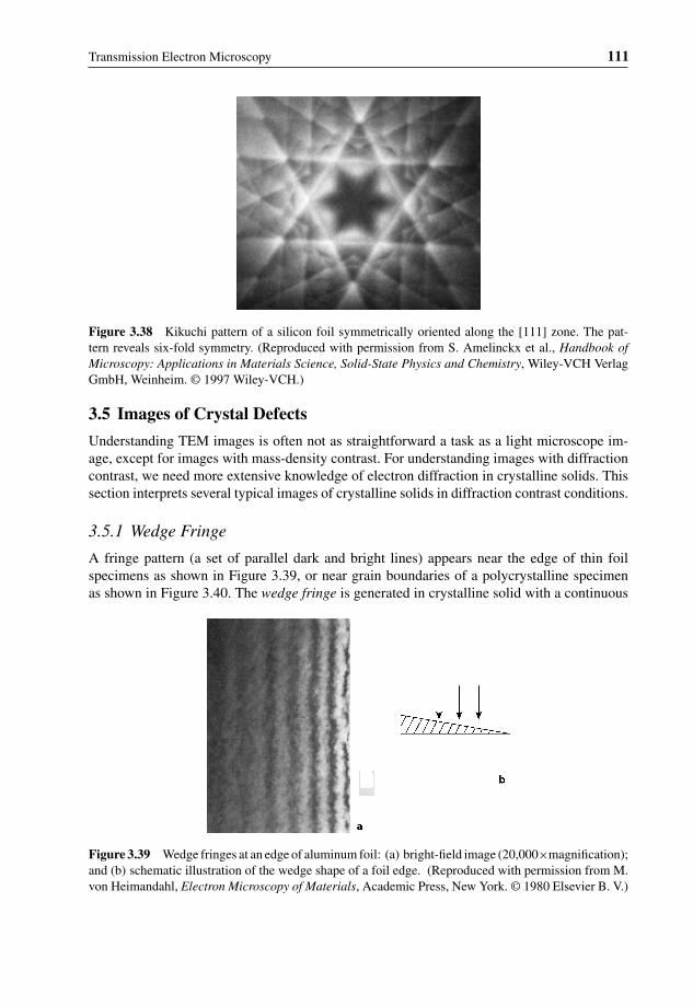
Kikuchi lines can be used to guide specimen tilting. For example, if the (hkl) plane is perfectlyparallel to the radiation cone at P, then I1 = I2. The difference between the dark and bright lineswill disappear. Figure 3.38 shows the Kikuchi pattern of silicon crystal with perfect alignmentof the electron beam along the crystal [111] zone axis. Note that the area between two lines isdarker than the background in the symmetric Kikuchi lines as shown in Figure 3.38. In suchpatterns, a lattice plane (hkl) parallel to the Kikuchi lines must be located at the center betweenthe lines. We can use the symmetrical patterns of Kikuchi lines centered at a point to obtainperfect alignment of the incident beam with a crystal zone axis.
Transmission Electron Microscopy 111
Figure 3.38 Kikuchi pattern of a silicon foil symmetrically oriented along the [111] zone. The pat-tern reveals six-fold symmetry. (Reproduced with permission from S. Amelinckx et al., Handbook ofMicroscopy: Applications in Materials Science, Solid-State Physics and Chemistry, Wiley-VCH VerlagGmbH, Weinheim. © 1997 Wiley-VCH.)
3.5 Images of Crystal Defects
Understanding TEM images is often not as straightforward a task as a light microscope im-age, except for images with mass-density contrast. For understanding images with diffractioncontrast, we need more extensive knowledge of electron diffraction in crystalline solids. Thissection interprets several typical images of crystalline solids in diffraction contrast conditions.
3.5.1 Wedge Fringe
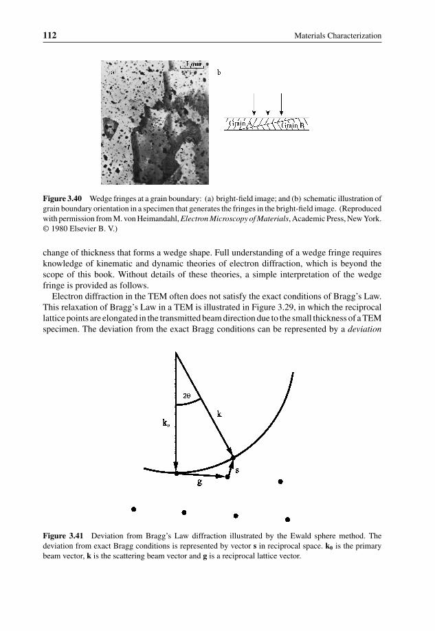
A fringe pattern (a set of parallel dark and bright lines) appears near the edge of thin foilspecimens as shown in Figure 3.39, or near grain boundaries of a polycrystalline specimenas shown in Figure 3.40. The wedge fringe is generated in crystalline solid with a continuous
Figure 3.39 Wedge fringes at an edge of aluminum foil: (a) bright-field image (20,000×magnification);and (b) schematic illustration of the wedge shape of a foil edge. (Reproduced with permission from M.von Heimandahl, Electron Microscopy of Materials, Academic Press, New York. © 1980 Elsevier B. V.)
112 Materials Characterization
Figure 3.40 Wedge fringes at a grain boundary: (a) bright-field image; and (b) schematic illustration ofgrain boundary orientation in a specimen that generates the fringes in the bright-field image. (Reproducedwith permission from M. von Heimandahl, Electron Microscopy of Materials, Academic Press, New York.© 1980 Elsevier B. V.)
change of thickness that forms a wedge shape. Full understanding of a wedge fringe requiresknowledge of kinematic and dynamic theories of electron diffraction, which is beyond thescope of this book. Without details of these theories, a simple interpretation of the wedgefringe is provided as follows.
Electron diffraction in the TEM often does not satisfy the exact conditions of Bragg’s Law.This relaxation of Bragg’s Law in a TEM is illustrated in Figure 3.29, in which the reciprocallattice points are elongated in the transmitted beam direction due to the small thickness of a TEMspecimen. The deviation from the exact Bragg conditions can be represented by a deviation
Figure 3.41 Deviation from Bragg’s Law diffraction illustrated by the Ewald sphere method. Thedeviation from exact Bragg conditions is represented by vector s in reciprocal space. k0 is the primarybeam vector, k is the scattering beam vector and g is a reciprocal lattice vector.
Transmission Electron Microscopy 113
Figure 3.42 Electron intensity oscillation in the thickness direction of a specimen. A wedge-shapedcrystal generates dark and bright fringes in the image because of the continuous change in thickness ofthe wedge.
vector (s) in reciprocal space as shown in Figure 3.41. The kinematic theory of diffractionindicates that the diffraction intensity periodically change with thickness of specimen (t).
Id ∝(
sin � st
� s
)2
(3.23)
s is the component of vector s parallel to the transmission vector ko as illustrated inFigure 3.41. For a given crystal orientation, s is a constant in Equation 3.23, and thus, theintensity of the diffracted beam must oscillate between zero and a maximum with thicknessincrease, as illustrated in Figure 3.42 . In a wedge-shaped crystal, we see a bright fringe wheret = ns−1 and a dark fringe where t = n + s
2 , in which n is an integer.The wedge fringe pattern is also seen at stacking faults. Stacking faults are a special type
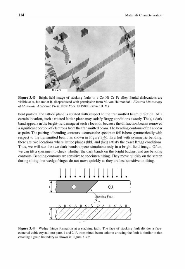
of planar defect in FCC crystals caused by disorder in the stacking sequence on the {111}planes. There is an interruption of the lattice structure at the fault plane. The stacking faultplane separates FCC crystal into two parts. Thus, the stacking fault plane is very similar to agrain boundary plane. Figure 3.43 shows a typical image of stacking faults that exhibit fringepatterns similar to a wedge fringe. The ends of fringes are the locations of partial dislocationsseparating a stacking fault from the rest of the crystal. Figure 3.44 schematically illustrates theformation of a wedge fringe when the stacking fault plane is inclined to the transmitted beam.The electron beam is intersected by the fault plane. The result will be generation of fringes inthe diffraction contrast image.
3.5.2 Bending Contours
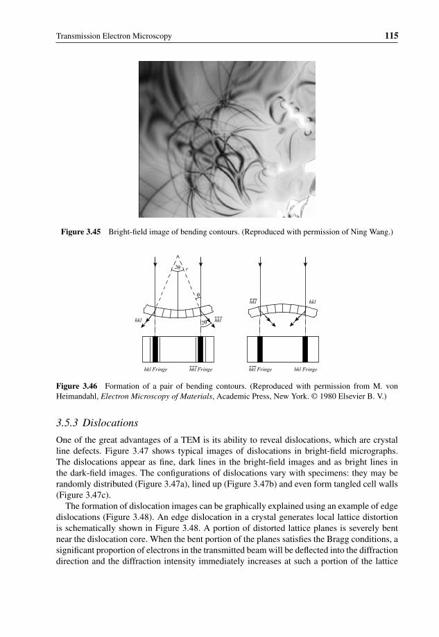
Dark bands in the background are often seen in images acquired in the diffraction contrast mode,as shown in Figure 3.45. The bands are called bending contours and commonly are diffuse andcurved. The bending contours result from the distorting or bending of a specimen foil. In the
114 Materials Characterization
Figure 3.43 Bright-field image of stacking faults in a Co–Ni–Cr–Fe alloy. Partial dislocations arevisible at A, but not at B. (Reproduced with permission from M. von Heimandahl, Electron Microscopyof Materials, Academic Press, New York. © 1980 Elsevier B. V.)
bent portion, the lattice plane is rotated with respect to the transmitted beam direction. At acertain location, such a rotated lattice plane may satisfy Bragg conditions exactly. Thus, a darkband appears in the bright-field image at such a location because the diffraction beams removeda significant portion of electrons from the transmitted beam. The bending contours often appearas pairs. The pairing of bending contours occurs as the specimen foil is bent symmetrically withrespect to the transmitted beam, as shown in Figure 3.46. In a foil with symmetric bending,there are two locations where lattice planes (hkl) and (
—hkl) satisfy the exact Bragg conditions.
Thus, we will see the two dark bands appear simultaneously in a bright-field image. Often,we can tilt a specimen to check whether the dark bands on the bright background are bendingcontours. Bending contours are sensitive to specimen tilting. They move quickly on the screenduring tilting, but wedge fringes do not move quickly as they are less sensitive to tilting.
t
t
Stacking Fault
A A
1 2
A AB B BC C C C A B
Figure 3.44 Wedge fringe formation at a stacking fault. The face of stacking fault divides a face-centered cubic crystal into parts 1 and 2. A transmitted beam column crossing the fault is similar to thatcrossing a grain boundary as shown in Figure 3.39b.
Transmission Electron Microscopy 115
Figure 3.45 Bright-field image of bending contours. (Reproduced with permission of Ning Wang.)
hkl Fringe hkl Fringe hkl Fringe hkl Fringe
2θ
θ
θ2 hkl
hklhkl
hkl
r
Figure 3.46 Formation of a pair of bending contours. (Reproduced with permission from M. vonHeimandahl, Electron Microscopy of Materials, Academic Press, New York. © 1980 Elsevier B. V.)
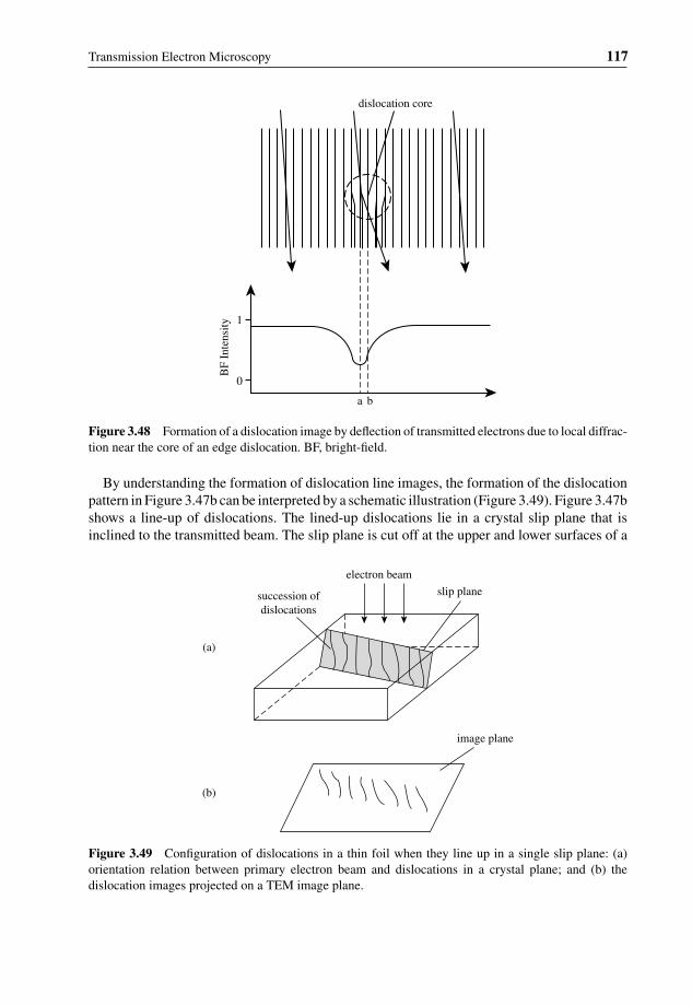
3.5.3 Dislocations
One of the great advantages of a TEM is its ability to reveal dislocations, which are crystalline defects. Figure 3.47 shows typical images of dislocations in bright-field micrographs.The dislocations appear as fine, dark lines in the bright-field images and as bright lines inthe dark-field images. The configurations of dislocations vary with specimens: they may berandomly distributed (Figure 3.47a), lined up (Figure 3.47b) and even form tangled cell walls(Figure 3.47c).
The formation of dislocation images can be graphically explained using an example of edgedislocations (Figure 3.48). An edge dislocation in a crystal generates local lattice distortionis schematically shown in Figure 3.48. A portion of distorted lattice planes is severely bentnear the dislocation core. When the bent portion of the planes satisfies the Bragg conditions, asignificant proportion of electrons in the transmitted beam will be deflected into the diffractiondirection and the diffraction intensity immediately increases at such a portion of the lattice

116 Materials Characterization
Figure 3.47 Bright-field images of dislocations: (a) in a Al–Zn–Mg alloys with 3% tension strain;(b) lining up in a Ni–Mo alloy; and (c) dislocation cell structure in pure Ni. (Reproduced with permissionfrom M. von Heimandahl, Electron Microscopy of Materials, Academic Press, New York. © 1980 ElsevierB. V.)
plane. Thus, in the bright-field image, a dark image forms at point a near the dislocation corelocation b as illustrated in Figure 3.48. Since the dislocation is a line defect, we should seea dark line which is extended into the plane of Figure 3.48. A screw dislocation also has adark line image for the same reason as an edge dislocation. A screw dislocation also bendslattice planes near its core to generate a plane orientation that satisfies the Bragg conditionslocally. The difference between an edge and screw dislocation is the bending direction, whichis determined by the Burger’s vector of dislocations.
Transmission Electron Microscopy 117
a
0
1
BF
Inte
nsity
dislocation core
b
Figure 3.48 Formation of a dislocation image by deflection of transmitted electrons due to local diffrac-tion near the core of an edge dislocation. BF, bright-field.
By understanding the formation of dislocation line images, the formation of the dislocationpattern in Figure 3.47b can be interpreted by a schematic illustration (Figure 3.49). Figure 3.47bshows a line-up of dislocations. The lined-up dislocations lie in a crystal slip plane that isinclined to the transmitted beam. The slip plane is cut off at the upper and lower surfaces of a
electron beam
slip plane
image plane
succession ofdislocations
(a)
(b)
Figure 3.49 Configuration of dislocations in a thin foil when they line up in a single slip plane: (a)orientation relation between primary electron beam and dislocations in a crystal plane; and (b) thedislocation images projected on a TEM image plane.

118 Materials Characterization
thin foil specimen. Thus, only a short section of dislocations in the slip plane can be seen onthe image screen of a TEM.
References
[1] Flegler, S.L., Heckman, Jr., J.W. and Klomparens, K.L. (1993) Scanning and Transmission Electron Microscopy,an Introduction, W.H. Freeman and Co., New York.
[2] von Heimandahl, M. (1980) Electron Microscopy of Materials, Academic Press, New York.[3] Goodhew, P.J. and Humphreys, F.J. (1988) Electron Microscopy and Analysis, 2nd edition, Taylor & Francis Ltd,
London.[4] Eberhart, J.P. (1991) Structural and Chemical Analysis of Materials, John Wiley & Sons, Chichester.[5] Spence, J.C.H. (1988) Experimental High-Resolution Electron Microscopy, 2nd edition, Oxford University
Express, Oxford.[6] Horiuchi, S. (1994) Fundamentals of High-Resolution Transmission Electron Microscopy, North-Holland,
Amsterdam.[7] Fultz, B. and Howe, J.M. (2001) Transmission Electron Microscopy and Diffractometry of Materials, Springer.[8] Shindo, D. and Oikawa, T. (2002) Analytical Electron Microscopy for Materials Science, Springer-Verlag, Tokyo[9] Brandon, D. and Kaplan, W.D. (1999) Microstructural Characterization of Materials, John Wiley & Sons,
Chichester.[10] Amelinckx, S., van Dyck, D., van Landuyt, J., van Tendeloo, G. (1997) Handbook of Microscopy: Applications
in Materials Science, Solid-State Physics and Chemistry, Wiley-VCH Verlag GmbH, Weinheim.
Questions
3.1 Generally, the wavelength of electrons (λ) and the acceleration voltage (Vo) has a relation-ship given by: λ ∝ 1/
√Vo. Do the values in Table 3.2 satisfy the relationship exactly?
Show the relationships between λ and Vo in Table 3.2 and compare them with valuesobtained from this relationship.
3.2 The resolution of a TEM is limited by diffraction (Rd) as discussed in Chapter 1,Equation 1.3, and by the spherical aberration which is expressed as: Rsph = Csα
3, where Cs
is the spherical aberration coefficient and α is the half-angle of the cone of light enteringthe objective lens. The TEM resolution is the quadratic sum of the diffraction resolution
and spherical aberration resolution, given by the expression: (R =√
R2d + R2
sph). The
minimum R is obtained when Rd∼= Rsph. Estimate the optimum value of α and resolution
limit of TEM at 100 and 200 kV. Cs ∼= 1 mm for an electromagnetic objective lens.3.3 Explain how is it possible to increase the contrast of a mass-density image. Can we obtain
a mass-density image of metal specimen? Can we obtain diffraction contrast in a polymerspecimen?
3.4 Note that both the mass-density and the diffraction contrast require only a transmittedbeam to pass through the objective aperture. How can you know you have diffractioncontrast without checking selected area diffraction (SAD)?
3.5 Sketch diffraction patterns of single crystals in a TEM for (a) a face-centered cubic (FCC)crystal with transmitted beam direction (B) parallel to [001], and (b) a body-centered cubic(BCC) crystal with B = [001].
3.6 Is a zone axis of a single crystal diffraction pattern exactly parallel to the transmittedbeam? Explain your answer graphically.
3.7 What kind of diffraction patterns you should expect if an SAD aperture includes a largenumber of grains in a polycrystalline specimen? Why?

Transmission Electron Microscopy 119
3.8 You are asked to obtain maximum contrast between one grain and its neighbors. Whichorientation of crystalline specimen do you wish to obtain? Illustrate your answer with apattern of single crystal diffraction.
3.9 You have been told that thickness fringe and bending contours can be distinguished.Explain how.
3.10 The reason we see a dislocation is that it bends a crystal plane near its core region. Indicatea case where we may not be able to see the dislocation in diffraction contrast under atwo-beam condition (a two-beam condition refers to a crystal orientation in which theintensity of one diffraction spot is much higher than those of the other diffraction spots).Indicate the answer either graphically or using the relation of vectors g (the normal ofplanes which generate the diffraction beam) and b (Burgers vector of dislocation).