InfraCal TOG/TPH Analyzers for Oil and Grease Measurements .

Application Note
Material Measurements with Vector Network Analyzers
The increasing popularity of mobile communications, wireless data transfers, and instant access technologies is giving rise to the need for faster data rates and more data channels to support an ever-increasing number of users and their devices. To meet these demands, circuits must be made smaller and perform faster than ever before. One way manufacturers accomplish this is by leveraging materials that have good dielectric properties (complex permittivity) in the components and devices used to build these circuits (e.g., FR 4 and RF Duroid among others). Another way is to design these components and devices at higher frequency ranges where more bandwidth is available to transfer data more efficiently. However, while manufacturers are quoting good permittivity of the existing materials at low frequencies, these same solutions may not be adequate for designing high-frequency RF and microwave applications.
This application note will examine the issues component and device manufacturers and their engineers will face when designing their solutions in higher frequencies.
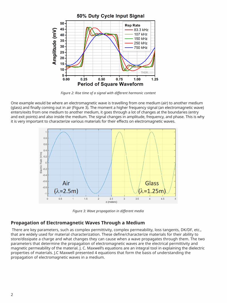
Material Effects on Electromagnetic WavesWhen designing components and devices for higher frequency ranges and increased bandwidth requirements, first a simple relationship between a time-domain signal (pulse signal or a 1/0 of digital domain) and the same signal in the frequency domain must be established (for the purpose of this paper, the details of the mathematics will not be detailed). The rise time of a signal in the time domain is inversely proportional to the number of odd harmonic frequency components and how close their amplitude levels are present in the frequency domain (see Figures 1 and 2). Operating at higher frequencies leads to smaller (faster) rise time and fall times, which is why data can be transferred more efficiently. However, if there is something that limits the rise time and fall times of a signal travelling through a medium, then it is important to understand the details of it.
Figure 1: Harmonic components in a signal
2
One example would be where an electromagnetic wave is travelling from one medium (air) to another medium (glass) and finally coming out in air (Figure 3). The moment a higher frequency signal (an electromagnetic wave) enters/exits from one medium to another medium, it goes through a lot of changes at the boundaries (entry and exit points) and also inside the medium. The signal changes in amplitude, frequency, and phase. This is why it is very important to characterize various materials for their effects on electromagnetic waves.
Propagation of Electromagnetic Waves Through a Medium There are key parameters, such as complex permittivity, complex permeability, loss tangents, DK/DF, etc., that are widely used for material characterization. These define/characterize materials for their ability to store/dissipate a charge and what changes they can cause when a wave propagates through them. The two parameters that determine the propagation of electromagnetic waves are the electrical permittivity and magnetic permeability of the material. J. C. Maxwell’s equations are an integral tool in explaining the dielectric properties of materials. J.C Maxwell presented 4 equations that form the basis of understanding the propagation of electromagnetic waves in a medium.
Figure 2: Rise time of a signal with different harmonic content
Figure 3: Wave propagation in different media
3
Where in these equation:
D (electric displacement field) = εE, (and ε = ε’-jε’’)
B (magnetic field) = µH (and µ = µ’-jµ’’)
J (current density) = σE
The equations imply that the interaction between a material and an electromagnetic wave depends on three primary quantities, namely: the permittivity (Ɛ), permeability (µ), and conductivity (σ). These parameters also depict the extent to which the electromagnetic wave can penetrate/propagate through a dielectric medium. Since the focus is mainly on dielectric materials, the discussion will be around permittivity and permeability as dielectrics are not conductive (or σ is extremely low). It is important to understand a little about the different kinds of materials before going in to the details of materials and their characterization.
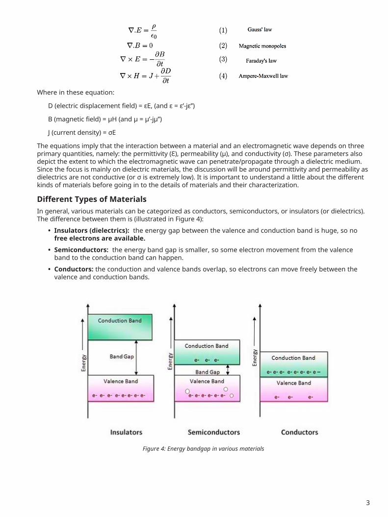
Different Types of Materials In general, various materials can be categorized as conductors, semiconductors, or insulators (or dielectrics). The difference between them is (illustrated in Figure 4):
• Insulators (dielectrics): the energy gap between the valence and conduction band is huge, so no free electrons are available.
• Semiconductors: the energy band gap is smaller, so some electron movement from the valence band to the conduction band can happen.
• Conductors: the conduction and valence bands overlap, so electrons can move freely between the valence and conduction bands.
Figure 4: Energy bandgap in various materials
4
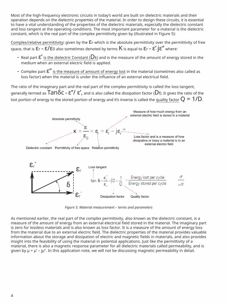
Most of the high-frequency electronic circuits in today’s world are built on dielectric materials and their operation depends on the dielectric properties of the material. In order to design these circuits, it is essential to have a vital understanding of the properties of the dielectric materials, especially the dielectric constant and loss tangent at the operating conditions. The most important parameter for a material is the dielectric constant, which is the real part of the complex permittivity given by (illustrated in Figure 5):
Complex/relative permittivity: given by the ɛr which is the absolute permittivity over the permittivity of free
space, that is ɛr = ɛ/ɛ0 also sometimes denoted by terms K is equal to ɛr = ɛ’-jɛ’’ where:
• Real part ɛ’ is the dielectric Constant (Dk) and is the measure of the amount of energy stored in the medium when an external electric field is applied.
• Complex part ɛ’’ is the measure of amount of energy lost in the material (sometimes also called as loss factor) when the material is under the influence of an external electrical field.
The ratio of the imaginary part and the real part of the complex permittivity is called the loss tangent,
generally termed as Tanδc = ɛ’’/ ɛ’, and is also called the dissipation factor (Df). It gives the ratio of the
lost portion of energy to the stored portion of energy and it’s inverse is called the quality factor Q = 1/D.
As mentioned earlier, the real part of the complex permittivity, also known as the dielectric constant, is a measure of the amount of energy from an external electrical field stored in the material. The imaginary part is zero for lossless materials and is also known as loss factor. It is a measure of the amount of energy loss from the material due to an external electric field. The dielectric properties of the material provides valuable information about the storage and dissipation of electric and magnetic fields in materials, and also provides insight into the feasibility of using the material in potential applications. Just like the permittivity of a material, there is also a magnetic response parameter for all dielectric materials called permeability, and is given by μ = μ’ – jμ’’. In this application note, we will not be discussing magnetic permeability in detail.
Figure 5: Material measurement – terms and parameters
5
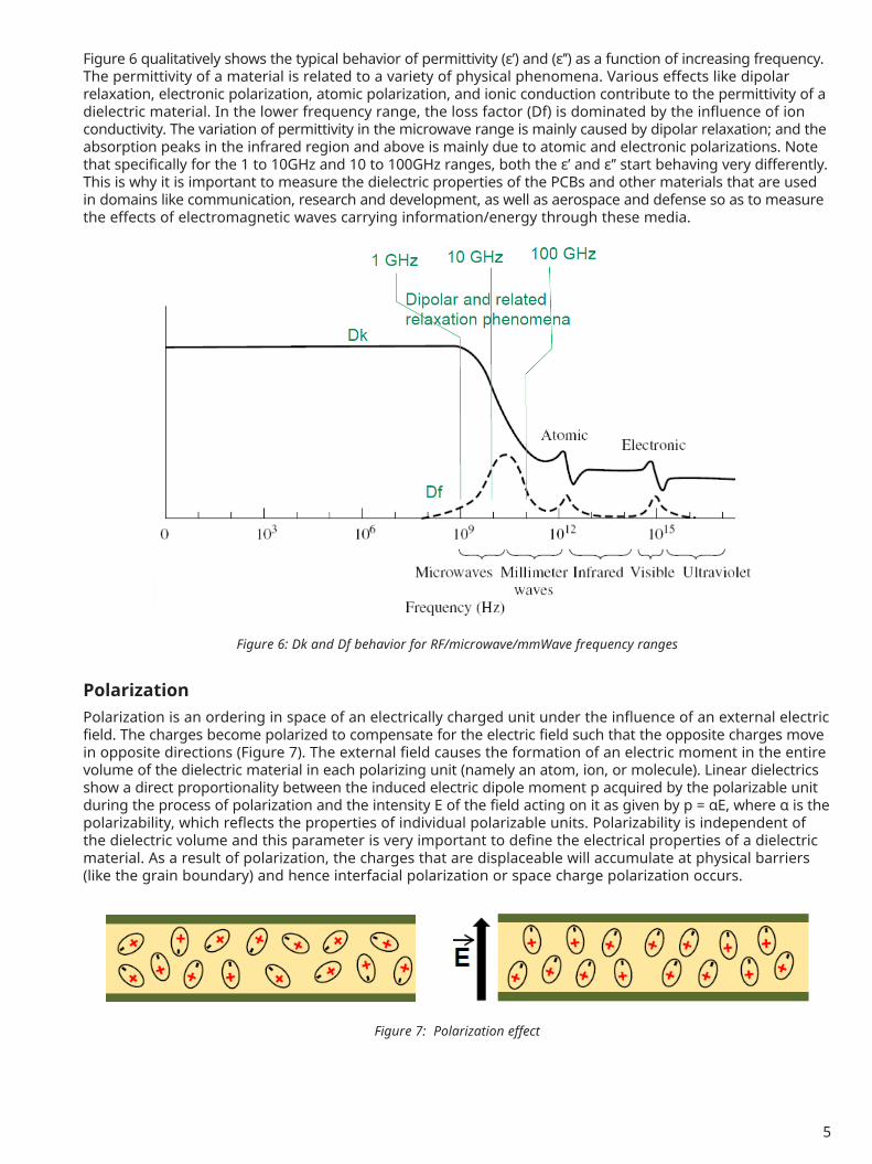
Figure 6 qualitatively shows the typical behavior of permittivity (ε’) and (ε’’) as a function of increasing frequency. The permittivity of a material is related to a variety of physical phenomena. Various effects like dipolar relaxation, electronic polarization, atomic polarization, and ionic conduction contribute to the permittivity of a dielectric material. In the lower frequency range, the loss factor (Df) is dominated by the influence of ion conductivity. The variation of permittivity in the microwave range is mainly caused by dipolar relaxation; and the absorption peaks in the infrared region and above is mainly due to atomic and electronic polarizations. Note that specifically for the 1 to 10GHz and 10 to 100GHz ranges, both the ε’ and ε’’ start behaving very differently. This is why it is important to measure the dielectric properties of the PCBs and other materials that are used in domains like communication, research and development, as well as aerospace and defense so as to measure the effects of electromagnetic waves carrying information/energy through these media.
PolarizationPolarization is an ordering in space of an electrically charged unit under the influence of an external electric field. The charges become polarized to compensate for the electric field such that the opposite charges move in opposite directions (Figure 7). The external field causes the formation of an electric moment in the entire volume of the dielectric material in each polarizing unit (namely an atom, ion, or molecule). Linear dielectrics show a direct proportionality between the induced electric dipole moment p acquired by the polarizable unit during the process of polarization and the intensity E of the field acting on it as given by p = αE, where α is the polarizability, which reflects the properties of individual polarizable units. Polarizability is independent of the dielectric volume and this parameter is very important to define the electrical properties of a dielectric material. As a result of polarization, the charges that are displaceable will accumulate at physical barriers (like the grain boundary) and hence interfacial polarization or space charge polarization occurs.
Figure 6: Dk and Df behavior for RF/microwave/mmWave frequency ranges
Figure 7: Polarization effect

6
The mechanism of polarization, which gives the dielectric constant, is different at different frequency regions. For example, dipole orientation and ionic conduction interact strongly at microwave frequencies (such as the dipole of water molecules, which rotate to follow an alternating electric field). This is the basic principle behind microwave ovens used for the warming of food. Atomic and electronic mechanisms are relatively weak. As frequency increases, the slow mechanisms lose effect and leave the faster ones to contribute to ε’. Based on the dipolar effect, the dielectric constant changes significantly at certain frequencies or will remain stable. Figure 8 depicts the different frequency regions and different polarization mechanisms.
Material Measurement Methods and TechniquesDielectric measurement is an important tool to understand material behavior, especially at high frequencies. This can provide the electrical or magnetic characteristics of the materials, which is a critical parameter required when implementing the material in applications. A number of methods have been developed to measure the complex permittivity/permeability of materials in the time/frequency domain based on reflection and reflection-transmission measurements.
For the dielectric measurement, one cannot rely on a single technique to characterize all the materials over a wide range of frequencies. The techniques and methods for measuring a lossy versus a low loss material can be totally different as will the accuracy of their results (there is always uncertainty in dielectric measurements while characterizing various materials; some significant factors that affect the accuracy of the measurements are frequency range, temperature, material nature, thickness, and size). Broadly speaking, material measurement methods can be divided into two categories: resonant and non-resonant.
• Resonant methods: limited by measurements on single/discrete frequency points, but very accurate.
• Non-resonant methods: measurements can be performed over a wide range of frequency, but normally used to observe the behavior of the EM waves.
Figure 8: Various polarization phenomenon at different frequency ranges

7
Resonant MethodsAs already mentioned, resonant methods are more accurate and precise in comparison to the non-resonant methods. Resonant methods generally include the resonator and the perturbation method.
1. The resonator method is based on the fact that the resonant frequency and quality factor of a dielectric resonator with given dimensions are determined by its permittivity and permeability. This method is often used to measure low loss dielectrics whose permeability is μ0.
2. The perturbation method is based on the resonant perturbation theory. For a resonator with given electromagnetic boundaries, when part of the electromagnetic boundary condition is changed by introducing a sample, its resonant frequency and quality factor will also be changed. From the changes of the resonant frequency and Q, the properties of the sample can be derived. This method is suitable for lower and moderate loss samples. There are further classifications of fixtures in the resonant perturbation method but those are out of the scope of this application note.
Resonant method includes five main families of resonant techniques:
1.) Micro strip type (Figure 9)
2.) Cavity resonator type (Figures 10 and 11)
Figure 9: Diagram of a micro strip type
Figure 10: TE01δ mode cavity resonator Figure 11: Open resonator method
Covering plate with pressure sensor
Resonator
Sample

8
3.) Dielectric resonators (Figure 12; note that the advantage of these methods lies in accessing the material from the resonator, as it is much simpler than in other devices; meaning the material is less likely to become damaged via insertion or removal)
4.) Open resonators, which also includes the Fabry-Perot resonator (Figure 13)
5.) Split post resonators (SPDR) are a very accurate measurement that can be performed as a function of temperature, however, as it is a resonant technique it can only be measured at one frequency (Figure 14)
Figure 14: 2 different types of split post resonators
Figure 12: 2 different setups for dielectric resonators
Figure 13: 2 different types of open resonators

9
How are Permittivity and Permeability Calculated?
In the cavity perturbation method, the sample under study is introduced into an antinode of the electric field or magnetic field, depending on whether permittivity or permeability is being measured.
If the sample under study is introduced at a junction with maximum electric field and minimum magnetic field, the electric properties (i.e. permittivity of the sample) can be characterized; if the sample is inserted into a place with maximum magnetic field and minimum electric field, the magnetic properties (permeability) of the sample can be characterized.
Non-Resonant MethodsIn non-resonant methods, the material properties are derived by the impedance and the wave velocities in the material. When a wave travels from one medium to another, both its impedance and velocity changes. Useful information can be deduced from the reflections and reflection transmission of the wave in the medium. Both permittivity and permeability can be calculated using this procedure.
Non-resonant methods mainly include reflection methods and transmission/reflection methods. In the reflection method, the material properties are calculated on the basis of the reflection from the sample. In the transmission/reflection method, the material properties are calculated on the basis of the reflection from the sample and the transmission through the sample.
• Reflection method: Electromagnetic waves are directed to a sample under study and the properties of the material sample are deduced from the reflection coefficient. Usually a reflection method can only measure one parameter, either permittivity or permeability. Two types of reflections are often used in materials property characterization, open- and short-circuit reflections, and the corresponding methods are called open-reflection method and shorted reflection method. As coaxial lines can cover broad frequency bands, coaxial lines are often used in developing measurement fixtures for reflection methods.
1. Open-reflection method: Figure 15 shows the basic measurement configuration of an open-reflection method. In actual applications, the outer conductor at the open end is usually made into a flange to provide suitable capacitance and ensure the repeatability of sample loading. The measurement fixture is called a coaxial dielectric probe. This method assumes that materials under measurement are non-magnetic and that interactions of the electromagnetic field with the non-contacting boundaries of the sample are not sensed by the probe.
It also assumes that the thickness of the sample should be much larger than the diameter of the aperture of the open-ended coaxial line, and, meanwhile, the material should have enough loss.
2. Shorted reflection method: the sample under study is usually electrically short, and this method is often used to measure magnetic permeability. In this method, the permittivity of the sample is not sensitive to the measurement results, and in the calculation of permeability, the permittivity is often assumed to be ε0
Probe
Material under test
1.85 mm connector;70 GHz
1 mm connector;110 GHz (125 GHz)
Figure 15: Basic measurement configuration of an open-reflection method
10
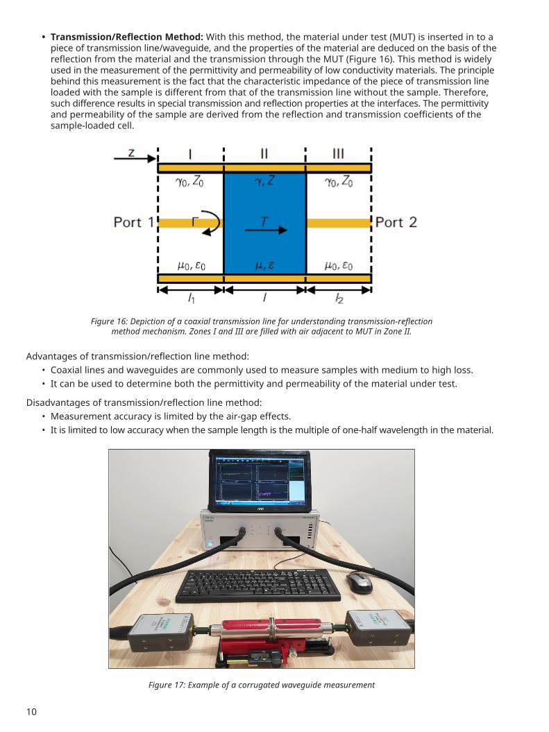
• Transmission/Reflection Method: With this method, the material under test (MUT) is inserted in to a piece of transmission line/waveguide, and the properties of the material are deduced on the basis of the reflection from the material and the transmission through the MUT (Figure 16). This method is widely used in the measurement of the permittivity and permeability of low conductivity materials. The principle behind this measurement is the fact that the characteristic impedance of the piece of transmission line loaded with the sample is different from that of the transmission line without the sample. Therefore, such difference results in special transmission and reflection properties at the interfaces. The permittivity and permeability of the sample are derived from the reflection and transmission coefficients of the sample-loaded cell.
Advantages of transmission/reflection line method: • Coaxial lines and waveguides are commonly used to measure samples with medium to high loss.• It can be used to determine both the permittivity and permeability of the material under test.
Disadvantages of transmission/reflection line method:• Measurement accuracy is limited by the air-gap effects.• It is limited to low accuracy when the sample length is the multiple of one-half wavelength in the material.
Figure 16: Depiction of a coaxial transmission line for understanding transmission-reflection method mechanism. Zones I and III are filled with air adjacent to MUT in Zone II.
Figure 17: Example of a corrugated waveguide measurement
11
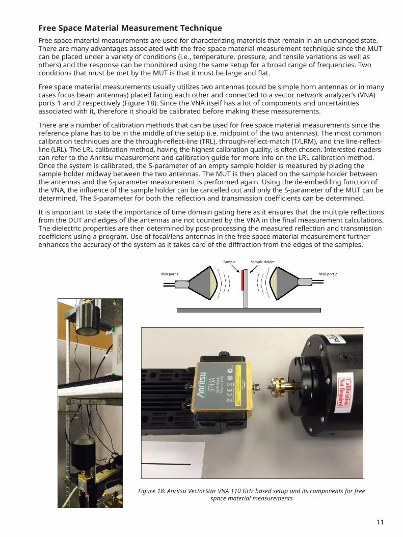
Free Space Material Measurement Technique Free space material measurements are used for characterizing materials that remain in an unchanged state. There are many advantages associated with the free space material measurement technique since the MUT can be placed under a variety of conditions (i.e., temperature, pressure, and tensile variations as well as others) and the response can be monitored using the same setup for a broad range of frequencies. Two conditions that must be met by the MUT is that it must be large and flat.
Free space material measurements usually utilizes two antennas (could be simple horn antennas or in many cases focus beam antennas) placed facing each other and connected to a vector network analyzer’s (VNA) ports 1 and 2 respectively (Figure 18). Since the VNA itself has a lot of components and uncertainties associated with it, therefore it should be calibrated before making these measurements.
There are a number of calibration methods that can be used for free space material measurements since the reference plane has to be in the middle of the setup (i.e. midpoint of the two antennas). The most common calibration techniques are the through-reflect-line (TRL), through-reflect-match (T/LRM), and the line-reflect-line (LRL). The LRL calibration method, having the highest calibration quality, is often chosen. Interested readers can refer to the Anritsu measurement and calibration guide for more info on the LRL calibration method. Once the system is calibrated, the S-parameter of an empty sample holder is measured by placing the sample holder midway between the two antennas. The MUT is then placed on the sample holder between the antennas and the S-parameter measurement is performed again. Using the de-embedding function of the VNA, the influence of the sample holder can be cancelled out and only the S-parameter of the MUT can be determined. The S-parameter for both the reflection and transmission coefficients can be determined.
It is important to state the importance of time domain gating here as it ensures that the multiple reflections from the DUT and edges of the antennas are not counted by the VNA in the final measurement calculations. The dielectric properties are then determined by post-processing the measured reflection and transmission coefficient using a program. Use of focal/lens antennas in the free space material measurement further enhances the accuracy of the system as it takes care of the diffraction from the edges of the samples.
Sample Sample Holder
VNA port 1 VNA port 2
Figure 18: Anritsu VectorStar VNA 110 GHz based setup and its components for free space material measurements

12
Measurement Setup for all Material Characterization1.) A high performance vector network analyzer with cables and calibration kit2.) MUT 3.) Material holder/fixtures based on the measurement techniques as per requirements4.) Software to run either on the VNA or on a standalone PC
VNA
Material Measurement Fixtures
Time domainrepresentation ofthe main beamresponse throughthe sample.
Frequency responsewith gating applied(main path only).
Figure 19: Time domain gating significance
Sample Sample Holder
VNA port 1 VNA port 2
1.85 mm connector;70 GHz
1 mm connector;110 GHz (125 GHz)

13
Software
In collaboration with third party solution providers, Anritsu can help customers with a complete solution for material characterization.
S. No. Material Measurement Method Frequency Range
Permittivity and Tan Delta Permeability
1 Free Space material measurement Up to 110 GHz Yes Yes
2 Various Resonant cavity (multiple solutions available) Up to 110 GHz yes Yes
3 Transmission line Method (supports co-axial and waveguide) Up to 110 GHz Yes Yes
4 Co-axial probe method Up to 110 GHz Yes
5 Parallel plate capacitor Up to 1 GHz Yes
6 Magnetic material characterization Up to 30 GHz Yes
7 Corrugated waveguide measurements Up to 1.1 THz Yes
SummaryThere are various methods of testing and characterizing a material under test. Concepts like polarization, permittivity, dielectric constant, and other key parameters were defined. Also discussed were specific procedures/fixtures for various materials and, depending upon their size/structure and type, the characterization can be done with varying levels of accuracy.
14
References: 1.) Evaluation of Microwave Characterization Methods for Additively Manufactured Materials by Chih-
Kuo Lee *, Jack McGhee , Christos Tsipogiannis, Shiyu Zhang , Darren Cadman , Athanasios Goulas , Tom Whittaker, Reza Gheisari, Daniel Engstrom, John (Yiannis) Vardaxoglou and William Whittow.
2.) Free-Space Materials Characterization by Reflection and Transmission Measurements using Frequency by- Frequency and Multi-Frequency Algorithms - by Fábio Júlio F. Gonçalves 1,2 ID , Alfred G. M. Pinto 2, Renato C. Mesquita 1 ID , Elson J. Silva 1 and Adriana Brancaccio 3.
3.) A Brief Review of Measuring Techniques for Characterization of Dielectric Materials byMuhammad Taha Jilani, Muhammad Zaka ur Rehman, Abid Muhammad Khan, Muhammad Talha Khan, Syed Muzamil Ali.
4.) Engineering and Tehcnology History Wiki
5.) Materials Characterization Using Microwave Waveguide System by Kok Yeow You
6.) Practical Measurements of Dielectric Constant and Loss for PCB Materials at High Frequency by Rogers Corporation.
7.) RF and Microwave Material Measurements: Techniques and Applications by Enrico Brinciotti
8.) Material Classification based on Energy Band Diagram on electricalvoice.com
9.) Microwave and Radio-Frequency Technologies in Agriculture: An Introduction for Agriculturalists and Engineers by Graham Brodie, Mohan V. Jacob, Peter Farrell.
10.) Microwave Electronics – Measurement and Material Characterization by L.F Chen, C.K Ong and C.P Neo ( NUS) , V.V Varadan and V.K Varadan ( Pennsylvania State university, USA)
11.) Measurement method of complex permittivity and permeability for a powdered material using a waveguide in microwave band by Hidetoshi Ebara *, Takao Inoue, Osamu Hashimoto.
12.) Keycom Charachteristic Technologies , Japan
13.) AET Inc. Japan
14.) Swissto12 , Switzerland
15.) Springer Handbook of Materials Measurement Methods by Horst Czichos, Tetsuya Saito, Leslie Smith (Eds.)
16.) Complex Permittivity Measurements with Split Split-Post Resonator by Dr. Jerzy Krupka ( Warsaw University of Technology, Poland)
17.) Frequency domain complex permittivity measurements at microwave frequencies by Dr. Jerzy Krupka , Department of Electronics and Information Technology, Institute of Microelectronics and Optoelectronics, Warsaw University of Technology, Koszykowa 75, 00-662 Warszawa, Poland.

11410-01190, Rev. A Printed in United States 2020-05©2020 Anritsu Company. All Rights Reserved.
® Anritsu All trademarks are registered trademarks of their respective companies. Data subject to change without notice. For the most recent specifications visit: www.anritsu.com
• United States Anritsu Company450 Century Parkway, Suite 190, Allen, TX 75013 U.S.A. Phone: +1-800-Anritsu (1-800-267-4878)
• Canada Anritsu Electronics Ltd.700 Silver Seven Road, Suite 120, Kanata, Ontario K2V 1C3, Canada Phone: +1-613-591-2003 Fax: +1-613-591-1006
• Brazil Anritsu Electrônica Ltda.Praça Amadeu Amaral, 27 - 1 Andar 01327-010 - Bela Vista - Sao Paulo - SP - Brazil Phone: +55-11-3283-2511 Fax: +55-11-3288-6940
• Mexico Anritsu Company, S.A. de C.V.Blvd Miguel de Cervantes Saavedra #169 Piso 1, Col. Granada Mexico, Ciudad de Mexico, 11520, MEXICO Phone: +52-55-4169-7104
• United Kingdom Anritsu EMEA Ltd.200 Capability Green, Luton, Bedfordshire LU1 3LU, U.K. Phone: +44-1582-433200 Fax: +44-1582-731303
• France Anritsu S.A.12 avenue du Québec, Batiment Iris 1-Silic 612, 91140 VILLEBON-SUR-YETTE, France Phone: +33-1-60-92-15-50 Fax: +33-1-64-46-10-65
• Germany Anritsu GmbHNemetschek Haus, Konrad-Zuse-Platz 1 81829 München, Germany Phone: +49-89-442308-0 Fax: +49-89-442308-55
• Italy Anritsu S.r.l.Via Elio Vittorini 129, 00144 Roma Italy Phone: +39-06-509-9711 Fax: +39-6-502-2425
• Sweden Anritsu ABIsafjordsgatan 32C, 164 40 KISTA, Sweden Phone: +46-8-534-707-00
• Finland Anritsu ABTeknobulevardi 3-5, FI-01530 VANTAA, Finland Phone: +358-20-741-8100 Fax: +358-20-741-8111
• Denmark Anritsu A/STorveporten 2, 2500 Valby, Denmark Phone: +45-7211-2200 Fax: +45-7211-2210
• Russia Anritsu EMEA Ltd. Representation Office in RussiaTverskaya str. 16/2, bld. 1, 7th floor. Moscow, 125009, Russia Phone: +7-495-363-1694 Fax: +7-495-935-8962
• Spain Anritsu EMEA Ltd. Representation Office in SpainEdificio Cuzco IV, Po. de la Castellana, 141, Pta. 5 28046, Madrid, Spain Phone: +34-915-726-761 Fax: +34-915-726-621
• United Arab Emirates Anritsu EMEA Ltd. Dubai Liaison Office902, Aurora Tower, P O Box: 500311- Dubai Internet City Dubai, United Arab Emirates Phone: +971-4-3758479 Fax: +971-4-4249036
• India Anritsu India Pvt Ltd.6th Floor, Indiqube ETA, No.38/4, Adjacent to EMC2, Doddanekundi, Outer Ring Road, Bengaluru – 560048, India Phone: +91-80-6728-1300 Fax: +91-80-6728-1301
• Singapore Anritsu Pte. Ltd.11 Chang Charn Road, #04-01, Shriro House Singapore 159640 Phone: +65-6282-2400 Fax: +65-6282-2533
• P. R. China (Shanghai) Anritsu (China) Co., Ltd.Room 2701-2705, Tower A, New Caohejing International Business Center No. 391 Gui Ping Road Shanghai, 200233, P.R. China Phone: +86-21-6237-0898 Fax: +86-21-6237-0899
• P. R. China (Hong Kong) Anritsu Company Ltd.Unit 1006-7, 10/F., Greenfield Tower, Concordia Plaza, No. 1 Science Museum Road, Tsim Sha Tsui East, Kowloon, Hong Kong, P. R. China Phone: +852-2301-4980 Fax: +852-2301-3545
• Japan Anritsu Corporation8-5, Tamura-cho, Atsugi-shi, Kanagawa, 243-0016 Japan Phone: +81-46-296-6509 Fax: +81-46-225-8352
• Korea Anritsu Corporation, Ltd.5FL, 235 Pangyoyeok-ro, Bundang-gu, Seongnam-si, Gyeonggi-do, 13494 Korea Phone: +82-31-696-7750 Fax: +82-31-696-7751
• Australia Anritsu Pty Ltd.Unit 20, 21-35 Ricketts Road, Mount Waverley, Victoria 3149, Australia Phone: +61-3-9558-8177 Fax: +61-3-9558-8255
• Taiwan Anritsu Company Inc.7F, No. 316, Sec. 1, NeiHu Rd., Taipei 114, Taiwan Phone: +886-2-8751-1816 Fax: +886-2-8751-1817
Specifications are subject to change without notice.