Master's Thesis Template - University of Oulujultika.oulu.fi/files/nbnfioulu-201706082647.pdf ·...
67
DEGREE PROGRAMME IN WIRELESS COMMUNICATIONS ENGINEERING MASTER’S THESIS LTE IMPLEMENTATION ON CGRA BASED SILAGO PLATFORM Author Muhammad Hasnain Ilyas Supervisor Prof. Jari Iinatti Second Examiner Dr. Kari Kärkkäinen Technical Advisor Dr. Syed M. Asad Hassan Jafri Examiner Prof. Ahmed Hemani MAY, 2017
Transcript of Master's Thesis Template - University of Oulujultika.oulu.fi/files/nbnfioulu-201706082647.pdf ·...

DEGREE PROGRAMME IN WIRELESS COMMUNICATIONS ENGINEERING
MASTER’S THESIS
LTE IMPLEMENTATION ON CGRA BASED
SILAGO PLATFORM
Author Muhammad Hasnain Ilyas
Supervisor Prof. Jari Iinatti
Second Examiner Dr. Kari Kärkkäinen
Technical Advisor Dr. Syed M. Asad Hassan Jafri
Examiner Prof. Ahmed Hemani
MAY, 2017

Ilyas M. (2017) LTE implementation on CGRA based SiLago platform. University
of Oulu, Degree Programme in Wireless Communications Engineering. Master’s
Thesis, 67 p.
ABSTRACT
This thesis implements long term evolution (LTE) transmission layer on a coarse
grained reconfigurable called, dynamically reconfigurable resource array
(DRRA). Specifically, we implement physical downlink shared channel baseband
signal processing blocks (PDSCH) at high level. The overall implementation
follows silicon large grain object (SiLago) design methodology. The methodology
employs SiLago blocks instead of mainstream standard cells. The main ambition
of this thesis was to prove that a standard as complex as LTE can be implemented
using the in-house SiLago framework. The work aims to prove that customized
design with efficiency close to application specific integrated circuit (ASIC) for
LTE can be generated with the programming ease of MATLAB. During this
thesis, we have generated a completely parametrizable LTE standard at high
level.
Key words: DRRA, SiLago, HLS, LTE, MIMO, OFDM.
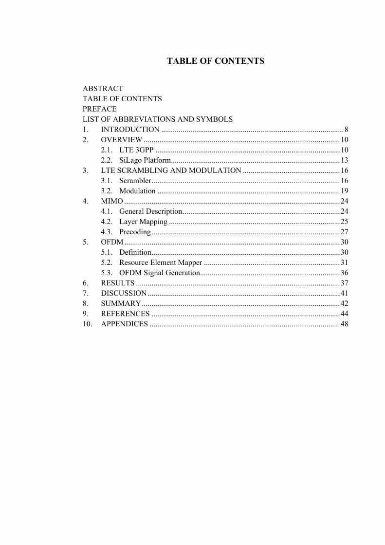
TABLE OF CONTENTS
ABSTRACT
TABLE OF CONTENTS
PREFACE
LIST OF ABBREVIATIONS AND SYMBOLS
1. INTRODUCTION .............................................................................................. 8
2. OVERVIEW ..................................................................................................... 10
2.1. LTE 3GPP ............................................................................................... 10
2.2. SiLago Platform ....................................................................................... 13
3. LTE SCRAMBLING AND MODULATION .................................................. 16
3.1. Scrambler ................................................................................................. 16
3.2. Modulation .............................................................................................. 19
4. MIMO ............................................................................................................... 24
4.1. General Description ................................................................................. 24
4.2. Layer Mapping ........................................................................................ 25
4.3. Precoding ................................................................................................. 27
5. OFDM ............................................................................................................... 30
5.1. Definition ................................................................................................. 30
5.2. Resource Element Mapper ...................................................................... 31
5.3. OFDM Signal Generation........................................................................ 36
6. RESULTS ......................................................................................................... 37
7. DISCUSSION ................................................................................................... 41
8. SUMMARY ...................................................................................................... 42
9. REFERENCES ................................................................................................. 44
10. APPENDICES .................................................................................................. 48

PREFACE
This Master thesis has been carried out at KTH royal institute of technology, Sweden
in partial fulfilment for the degree towards Master’s Degree Programme in Wireless
Communications Engineering from University of Oulu, Finland. First of all, I would
like to thanks Prof. Jari Iinatti for supervising this thesis and his excellent guidance to
finalize this work. I would also like to thanks my second examiner Dr. Kari Kärkkäinen
for his useful comments. I would like to thanks Prof. Ahmed Hemani to give me an
opportunity to complete this thesis work under his research group at KTH institute.
Many thanks to Dr Syed M. Asad Hassan Jafri for his excellent support, guidance,
encouragement and advices during each step of this work.
I would not be able to say “thanks” to my parents, beloved sisters and my brother.
Their love, prayers and kindness for me are beyond limitations. At the end I would like
to dedicate this intellectual effort to my mentor “ Prof. Ahmed Rafique Akhtar”.
Oulu, MAY 2017
Muhammad Hasnain Ilyas

LIST OF ABBREVIATIONS AND SYMBOLS
𝑎𝑘(𝑚) complex modulation symbol during the mth OFDM symbol interval
𝑏(𝑞) block of bits
𝑐(𝑛) final scrambling sequence
𝐶𝑖𝑛𝑖𝑡 second m-sequence initialization of scrambler
k resource element with frequency-domain index k
l resource element with time-domain index l
𝑀𝑠𝑦𝑚𝑏𝑎𝑝
number of modulation symbols to transmit per antenna port
𝑀𝑠𝑦𝑚𝑏𝑙𝑎𝑦𝑒𝑟
number of modulation symbols to transmit per layer
𝑁𝑐 number of subcarriers
𝑁𝐼𝐷𝑐𝑒𝑙𝑙 physical layer cell identity
𝑁𝑆𝑦𝑚𝑏𝐷𝐿 number of OFDM symbols in downlink slot
𝑁𝑅𝐵𝐷𝐿 downlink bandwidth configuration, expressed in multiples of 𝑁𝑆𝐶
𝑅𝐵
𝑁𝑆𝐶𝑅𝐵 resource block size in frequency domain, as a number of subcarrier
𝑛𝑠 subframe number
𝑛𝑅𝑁𝑇𝐼 radio network temporary identifier
𝑞 codeword number
𝑇𝑢 modulation symbol rate of considered OFDM subcarrier
v number of transmission layers
W precoding matrix for downlink spatial multiplexing
𝑥1 first m-sequence of scrambler
𝑥2 second m-sequence of scrambler
Δ𝑓 subcarrier spacing
3GPP third generation partnership project
4G fourth generation
5G fifth generation ASIC application specific integrated circuits
AlgoSil algorithm to silicon
BER bit error rate
BW band width
CDD cyclic delay diversity
CGRA coarse grain reconfigurable architectures
CP cyclic prefix
CQI channel quality indicator
CRC cyclic redundancy check
CRS cell specific reference signal
DC direct current
DCI downlink control information
DFT discrete fourier transforms

DiMArch distributed memory architecture
DPU data path unit
DRRA dynamically reconfigurable resource array
DSP digital signal processor
EDA electronic design automation
eNodeB evolved node b
FDD frequency division duplexing
FPGA field programmable gate array
FFT fast fourier transform
FDM frequency division multiplexing
HLS high level synthesis
IFFT inverse fast fourier transform
ITRS international technology roadmap for semiconductors
ISI inter symbol interference
LTE long term evaluation
LFSR linear feedback shift register
LUT lookup tables
MAC medium access layer
MAC multiply and accumulate unit
MIMO multiple input multiple output
OFDM orthogonal frequency division multiplexing
PAPR peak to average power ratio
PBCH physical broadcast channel
PCFICH physical control format indicator channel
PDSCH physical downlink shared channel
PDCCH physical downlink control channel
PMCH physical multicast channel
PMI precoder matrix indicator
PHICH physical hybrid indicator channel
QAM quadrature amplitude modulation
QPP quadrature permuted polynomial
QPSK quadrature phase shift keying
RE resource element
REG resource element group
RB resource block
RTL register transfer level
RFIE register file
RS reference signals
SiLago silicon large grain object
SRAM static random access memory
SYLVA system level synthesis
SCFDM single carrier frequency division multiplexing
SSS secondary synchronization signal

TDD time division duplexing
VLSI very large scale integration
VHDL very hardware description language

1. INTRODUCTION
Long term evolution (LTE) is known as the 4th generation cellular technology. It is
the latest wireless communication standard, which is developed by third generation
partnership project (3GPP). LTE technology has been covered most of the end user
demands in terms of better spectral efficiency and maximum throughput. Further
improvements in LTE leads fourth generation (4G) technology towards the 5th
generation (5G). The standardization for upcoming 5G technology is underway and
shall be completed by 2020 [1].
Different design challenges should be considered as in particular from the
implementation perspective of LTE on the architecture level, where energy efficiency
and computational complexity like problems are still demand to be investigated on
different digital signal processing platforms [2]. In general, baseband signal processing
algorithms of LTE and the other previous wireless standards are implemented on
application specific integrated circuits (ASICs), field programmable gate arrays
(FPGAs) and digital signal processors (DSPs) [3]. ASIC has the lack of flexibility as
compared to FPGA and on the other side FPGA is less efficient in performance
compared to ASIC [4].
Coarse grained reconfigurable architectures (CGRAs) [5] may be considered for
the implementation of DSP applications in future. These CGRAs have the efficiency
close to ASICs and also have an advantage of flexibility like FPGA. Meanwhile, the
cost of CGRAs is quite low as compared to ASICs [6]. On the other hand, international
technology roadmap for semiconductors (ITRS) [20] has pushed the very large scale
integration (VLSI) community to set new targets by 2020 in terms of performance
improvement while the design effort remains constant. These targets are also
compelled the VLSI community to look out new architectural innovations [20].
A recently developed heterogeneous dark silicon [7] aware coarse grain
reconfigurable fabric is proposed to fulfils the ITRS goals [8, 20]. This CGRA fabric
provides micro architecture level hardware centric customization by SiLago platform
[23]. It is also known as high-level synthesis methodology from broader perspective.
Moreover, customization cost is also reduced by SiLago method. SiLago method is
produced a timing and DRC clean GDSII design by using the large grain micro
architecture level hardened and characterized blocks. The abstraction gap between
Simulink and physical design level is reduced. It shows 2 to 3 orders improvement in
synthesis efficiency as well as ability to precisely predict cost metrics. This platform
is also used to analysis the system level area, energy and latency of different DSP
algorithms [9].
As mentioned before, implementing complex signal processing algorithms on
architectural level is a great challenge. VLSI community is trying to solve this problem
by providing alternate approaches like high-level synthesis (HLS). HLS tools directly
map the algorithm to the hardware. In general algorithm is written in any high-level
language and mapped onto hardware by a HLS tool. In our case, one algorithm is
modeled one MATLAB function and will be implemented on hardware. SiLago
platform is proposed for this purpose. This master thesis addresses the issue related to
HLS in particular with SiLago platform’s perspective by using the basic
implementation of LTE physical downlink baseband signal processing blocks.
This thesis provides a deep understanding from theoretical to implementation
perspective of LTE. Signal processing blocks are considered to bridge the gap between

9
algorithm development and its implementation from low level to high level
perspective. The key points of this thesis are summarized as follows.
3GPP standard analysis for considered signal processing blocks.
Development of MATLAB codes for the SiLago platform.
Overview of data communication and management flow on architecture level.
Modeling the signal processing blocks on Simulink.
Verification of the correct functionality of developed MATLAB codes with
golden model MATLAB codes for SiLago platform.
The rest of this thesis report is organized as follows: Chapter 2 explains the SiLago
platform overview and LTE physical layer signal processing blocks. Chapter 3 covers
the LTE scrambler and mapper implementation. In Chapter 4 MIMO introduction and
the related signal processing blocks are discussed. Finally, Chapter 5 explains the
OFDM technology and implementation overview from transmission side. At the end,
Chapter 6 describes the results section. Discussion of the thesis is also included in
Chapter 7 where the conclusion and future work is also presents. At the end Chapter 8
provides the summary of the thesis.

10
2. OVERVIEW
This chapter describes the background information, for the development of more
understanding towards the thesis. First part of this chapter in Section 2.1 is specifically
explained the LTE baseband transmission side, which further describes that which
signal processing blocks are going to be considered for the implementation on
considered signal processing platform. While second part of this chapter in Section
2.2, explains the detail of SiLago platform, as exploring the information related to
understands the considered signal processing platform.
2.1. LTE 3GPP
Wireless communications standards are emerging after the introduction of 1G standard
in 1980. 1G standard was based on analogue technology while digital technology is
introduced in second generation wireless systems. After the evaluation of second
generation world experienced the broadband data wirelessly in 3G systems, as the
Figure 1 shows the evaluation of cellular technology, adopted from [10]. LTE/LTE
advanced released by 3GPP has successfully launched the 4G systems globally with
the enhancement of previous wireless standards. Now the emerging trends are near
approaching to introduce the 5G systems with new developments from each aspect of
existing LTE systems. [11]
Figure 1. Evolution of Mobile communication standards.
Whereas LTE has introduced the new technologies e.g. MIMO, OFDMA, turbo
coding etc. These technological innovations are related to the physical layer of LTE.
Physical layer is dealt with the all processing data bit wise from the higher layers.
Different signal processing techniques are implemented on physical layer data for the
successful transmission and reception of LTE system.

11
LTE Physical Layer
LTE physical layer signal processing chain is related with the uplink and downlink
data transmission from mobile terminal(UE) to base station (eNodeB) and base station
to mobile terminal respectively. In signal processing chain the only difference between
the uplink and downlink as an additional discrete fourier transform (DFT) block in
uplink side for reducing of peak-to-average power ratio (PAPR) [12]. High PAPR is a
bottleneck of OFDM technology. Therefore, many different schemes are proposed for
reducing PAPR. This is the reason why in uplink side introducing an external signal
processing block. Uplink transmission generates the single carrier frequency division
multiplexing (SCFDM) symbols as compared to the downlink side while downlink
transmission produces the orthogonal frequency division multiplexing (OFDM)
symbols. [13]
Figure 2 represents the LTE physical layer transmitter model both for uplink and
downlink transmission from signal processing chain perspective. Whereas it is obvious
that the specifications for each block are different both for uplink and downlink side,
standardization details can be found in [14, 15].
Figure 2. Generic overview of LTE transmitter side physical layer.
Physical layer processing is taken into account when data is arrived in form of
transport blocks from the medium access control (MAC) layer. Data is consisted on
different number of bits and one transport block is known as one code word and either
one or two code words can be processed, it depends on the scheduling. A very general
description of these signal processing blocks is given in Table 1. [11, 13]

12
Table 1. LTE transmission side signal processing block description
CRC
attachment
A 24-bit cyclic redundancy check (CRC) is attached to each
transport block, in particular before the insertion of data in
channel coding (Turbo encoder) block. This process is helpful at
receiver side for early termination of turbo decoding iterations,
hence computational complexity of turbo decoding procedure
sort out.
Code-block
segmentation
This block will be only activated if the inserted data from MAC
layer is exceeded from the defined range of bits for turbo encoder,
hence this block segmentation divides the number of bits into
smaller blocks then CRC appended once again and data bits are
inserted into turbo encoder in channel coding block.
Channel coding Channel coding in LTE is based on turbo encoding. Turbo
encoder is used for this process which consist on a LTE QPP
internal inner interleaver, sandwiched between two eight state
constituent encoders. Overall turbo encoder rate is 1/3, while
constituent encoders have two rate-1/2.
Rate matching Rate matching is used to adjust or meet the coding rate
requirement as according to the scheduling which is based upon
channel condition. Three sub block inter leavers are used to
collect the three output bits from turbo encoder, known as
systematic, first and second parity bits. Circular buffer is used for
the desired code rate, used puncturing or repeating method.
Code-word
reconstruction
Code word reconstruction block is implemented after rate
matching block and is used to concatenating the code blocks
which come outs from rate matching block for further processing.
Scrambler Scrambler block produces the scrambling sequences and these
bits are multiplied (exclusive or operation) with coming code
word bits. This block helps out to randomized the interferences.
Mapper In this block, three modulation schemes as quadrature phase shift
keying (QPSK), quadrature amplitude modulation (QAM)-16
and QAM-64 are used to mapped the scrambled bits to the
complex modulated symbols.
Layer Mapper This section divides the modulated symbols on to different layers
for the requirement as for MIMO transmission mode.
DFT DFT block used in uplink transmission and converts the layer
mapper symbols from frequency domain to time domain
symbols.
Precoding Precoding section is used to multiplied the symbols with a certain
matrix which holds the characteristics of desired MIMO
transmission scheme.
Resource
Element
Mapper
Different symbols from different channels with reference and
synchronization signals are re arranged according to the MAC
scheduler.
OFDM/SCFDM
signal
generation
FFT/IFFT butterfly is used for the transformation of the arranged
symbols to the time domain signal. At the end, cyclic prefix (CP)
is inserted in each OFDM symbol.

13
While in this master thesis only considered the downlink transmission chain for the
implementation side on SiLago platform as shown in Figure 3. From scrambler to
OFDM signal generation all the algorithms are modified according to the SiLago
platform.
Figure 3. PDSCH signal processing blocks.
Receiver side base band signal processing involved very complex algorithms. The
complexity issues are discussed in detail in [16]. However, the receiving side
algorithms implementation is out of scope at this time.
2.2. SiLago Platform
This introduction describes a brief overview of SiLago platform; explanation of
different terms is only focused, which are used throughout in this master thesis while
the complete references are given for further detail.
A SiLago platform has been developed [17] which is based on coarse grain
reconfigurable computation and storage fabrics, as dynamically reconfigurable
resource array (DRRA) and distributed memory architecture (DiMArch) respectively
as shown in Figure 4 [17].
Figure 4. Main elements of SiLago Platform.

14
DRRA
Dynamically reconfigurable resource array (DRRA) [18] is known as parallel
distributed digital signal processing (PDDSP) fabric. It is based upon the CGRA cell
and each cell holds one register file, one data path unit (DPU), four address generation
units (AGUs) and one sequencer. The number of cells are dependent on the
requirements of the application. [19]
DPUs: Data path units [20] are basically designed for the implementation of
DSP algorithms. Whereas these are 16-bit integer units with four 16 bit inputs
and two 16 bit outputs. In general, DPU consists of two sections as one is
known as arithmetic section which deals with different arithmetic operations
such as, butterfly operations for FFT/IFFT, MAC, add, subtract, sum of
difference etc. Other section of DPU is consist on logical section which deals
with logical instructions and single bit shift operations. DPU is also performs
the overflow/underflow, saturation, truncation/rounding check [19].
Register file: Register file [21] of DRRA is 64 word 16-bit register file
including with two read and two write ports. It is used to provide the data to
DPU for the processing. Register file is also holds the AGU which generates
the addresses for read and write ports [19].
DiMArch
DiMArch [22] known as distributed memory architecture which provides the external
large memory to DRRA fabric. This fabric is consisted on static random access
memory (SRAM) banks which are interconnected by two network on chips (NOCs).
One is known as circuit switched NOC which is used to transfer the data between
SRAM banks and DRRA register files. Other NOC known as packet switch control
NOC which is used to configure the data.
SiLago Design Methodology
SiLago blocks are consisted on arithmetic logic units, register files, sequencer,
interconnect elements etc. These blocks are considered as micro architectural level
design units that replaces standard cells. Whereas micro architectural operations are
divided into three main categories known as computation, storage and configuration.
Computation part is dealt with DRRA operations, in which data is route from register
file to DPU for computation and then data is routing back to a register file or transfer
to the another DPU. Storage unit is used to process the data from storage blocks as
data is moved between SRAM bank to SRAM bank in DiMArch region or SRAM
bank to register file and register file to SRAM bank. [17]
Figure 5 [17] represents the SiLago design methodology which consists of three
major steps. In first step SiLago blocks are hardened and characterized by
RTL/Logic/Physical EDA flow [9]. For this step this master thesis also put some effort
to investigates how considered signal processing blocks are going to be hardened for
SiLago platform.

15
Figure 5. SiLago Design flow.
In second step on the basis of these blocks a general library of signal processing
algorithm is created by the algorithm to silicon (AlgoSil) tool. AlgoSil synthesizes
hardware which is based on SiLago blocks of an algorithm/function from MATLAB
[17]. Major contribution in this thesis for the developments of MATLAB codes for
considered signal processing blocks, which helps out to synthesize the hardware.
In final step a system level synthesis tool known as SYLVA [24] is used. Simulink
model or application is fed into the SYLVA as input. SYLVA decides the best
functions from AlgoSil developed library for Simulink model then perform execution
processes [24]. At the end, SiLago platform generates the macro GDSII and reports
mainly in terms of system level area, energy, latency etc. For the result section, chosen
signal processing blocks are modeled in Simulink. In addition, for the results we also
taken the assumptions of different parameters of signal processing blocks for the
generation of different functional implementations by SYLVA tool.

16
3. LTE SCRAMBLING AND MODULATION
Scrambling and modulation blocks are investigated in detail from LTE implementation
perspective, based upon 3GPP standardization parameters. First part of this chapter is
consisted on LTE scrambler part and the second part of the chapter is dealt with
modulation detail of LTE. The main idea in this chapter is just to show how the basic
implementation of these blocks are taken place at low level.
3.1. Scrambler
Scrambler is the first signal processing block in physical downlink processing chain
as shown in Figure 6. This block generates the scrambling sequence, which is
implemented on each bit of every code word. In general, scrambler is used to reduce
the interference between transmitted data, that is the reason scrambling sequences are
increases the randomness of transmitted bits. [10]
Figure 6. Scrambler block in PDSCH signal processing chain.
Scrambling sequence is pseudo random and generated by the length-31 Gold
sequence. The overall procedure for this operation is given in [14] and also described
as
𝑥1(𝑛 + 31) = (𝑥1(𝑛 + 3) + 𝑥1(𝑛))𝑚𝑜𝑑2 (3.1)
𝑥2(𝑛 + 31) = (𝑥2(𝑛 + 3) + 𝑥2(𝑛 + 2) + 𝑥2(𝑛 + 1) + 𝑥2(𝑛))𝑚𝑜𝑑2. (3.2)
The above equations are the m-sequences and also the polynomials of linear
feedback shift registers (LFSR) for hardware implementation side, which finally
produces the scrambling sequence according to
𝑐(𝑛) = (𝑥1(𝑛 + 𝑁𝑐) + 𝑥2(𝑛 + 𝑁𝑐))mod2, (3.3)
Where 𝑐(𝑛) represents the final scrambling sequence of length 𝑀𝑝𝑛 𝑤ℎ𝑒𝑟𝑒 𝑛 =
0,1, … , 𝑀𝑝𝑛 − 1. Moreover, 𝑁𝑐 = 1600 which explains the initializations of m-
sequences, which are taken place 1600 times. The initializations of m-sequences are
also standardized according to LTE specifications as below.
First m-sequence (𝑥1) initializations will be as

17
𝑥1(0) = 1, 𝑥1(𝑛) = 0, 𝑛 = 1,2 , … ,30,
Second m-sequence initialization depends on different parameters and transport
channel type; this initialization is denoted by 𝐶𝑖𝑛𝑖𝑡.
This condition is elaborated from parameters perspective as
𝐶𝑖𝑛𝑖𝑡 = {𝑛𝑅𝑁𝑇𝐼 . 214 + 𝑞. 213 + (𝑛𝑠/2). 29 + 𝑁𝐼𝐷𝑐𝑒𝑙𝑙} for PDSCH
𝐶𝑖𝑛𝑖𝑡 = {(𝑛𝑠/2). 29 + 𝑁𝐼𝐷𝑀𝐵𝑆𝐹𝑁}. for PMCH
Parameters which are used in 𝐶𝑖𝑛𝑖𝑡 are available in detail in different research papers
as [25, 26], here is just mentioned the functionality of these parameters in Table 2.
Table 2. LTE scrambler parameters description for second initial condition
Parameter Description
𝑛𝑅𝑁𝑇𝐼 Radio network temporary identifier is functionally corresponding user
equipment (UE) with physical downlink control channel (PDCCH);
value is used to describes the resource allocation for PDCCH.
𝑞 Number of code words, one code word consists on one block of bits.
Two code words used for spatial multiplexing.
𝑛𝑠 Number of sub frames which could be any value from 0 to 9, as one
LTE frame is consists of 10 sub frames.
𝑁𝐼𝐷𝑐𝑒𝑙𝑙 Cell Identity associated with synchronization signals, acknowledging
about Cell ID Group and Cell ID Sector.
Equation (3.3) is the output of Gold sequence which is implemented for each code
word. This implementation is done by exclusive or operation according to [14] as
described in
�̃�(𝑞)(𝑖) = (𝑏(𝑞)(𝑖) + 𝑐(𝑞)(𝑖)) 𝑚𝑜𝑑2. (3.4)
Where q is code word and 𝑏(𝑞) represents the block of bits,
𝑏(𝑞)(0), … , 𝑏(𝑞) (𝑀𝑏𝑖𝑡(𝑞)
− 1) , where 𝑀𝑏𝑖𝑡(𝑞)
is bit number in code word q. Code word q
is exclusive or with generated gold sequence and finally scrambled bits are come out
from scrambler block and represented with �̃�(𝑞). This scrambled bit sequence will be
transmitted in one sub frame and the same procedure is also possible if the number of
code words are two but in that particular case the value of q in 𝐶𝑖𝑛𝑖𝑡 will be equal to 1
else if code word is one block then the value of q will be 0 as 𝑞𝜖{0,1} [14]. Figure 7 shows the overall operation which already explained above. This Figure
represents the LFSR 1 (x1) and LFSR 2 (x2) operation with respective initialized
values and specified polynomials according to the LTE specifications. Finally, at the
end scrambled output bits are generated.

18
Figure 7. Representation of Scrambling Operation.
Implementation Aspect
As far as implementation on SiLago hardware is concerned, the static initialization
condition for LFSR 1 is stored in register file section. For parameters, dependent
initialization should be calculated from initialization calculator for LFSR 2, the values
for these parameters could be chosen in Table 3 [14] final output from the calculation
should be equal to the 32-bit array.
Table 3. Parameter values for calculation
Parameter Values
𝑛𝑅𝑁𝑇𝐼 Type is integer range could be any value in range [0, 65535].
𝑞 Type is integer and the value either [0,1].
𝑛𝑠 Sub frame index integer type value chosen from [0,9].
𝑁𝐼𝐷𝑐𝑒𝑙𝑙 Consist on CellID_Group and CellID_Sector and the ranges for both
parameters are in the range of [0,167] and [0,2] respectively. Finally
calculated according to (3* CellID_Group + CellID_Sector). Or
directly selected Cell ID in the range of [0,503].
The second initialization is run time decision which depends on the different
parameters and different channel types [14]. All parameter values for initial condition
are stored initially in register file section and the calculation equation is implemented
on DPU. Output of gold sequence generation is calculated according to the Equation
(3.3). Finally, at the end scrambler sequence is exclusive-or with input code word bits.
The input code word bits are also stored in register file section.
Figure 8 represents the hardware structure for designing the LTE scrambler block
on SiLago platform. One point is note that register file element has 16-bit value and
LTE specified LFSR has 32 bit, for this problem we can store all operations with two
elements jointly in register file section.

19
Figure 8. Hardware Implementation of LTE scrambler block.
At the end MATLAB code is modified for the system level synthesis (SYLVA)
compiler. Original MATLAB version code of scrambling block is available in [13].
But according to SiLago platform, modification is done as available in Appendix 1.
This code explains that input code word bits are stored in memory and the size of
memory is dependent on the length of code word bits. Register file has 64 elements
and in each element, 16-bit value is stored. According to that parameter, register file
size is parametric which depends on the number of code word bits. Secondly, each
initialization condition is also stored in two elements. Output scrambled bits has the
same size as the input code word bit length.
3.2. Modulation
After scrambling the code word block, the next procedure is mapping these bits for the
modulation process. LTE mapper is the next block after the scrambling block for the
implementation of modulation as shown in Figure 9.
Figure 9. LTE Mapper block on PDSCH signal processing chain.
Three types of modulation schemes are used in LTE according to the 3GPP
specifications [14] as are, quadrature phase shift keying (QPSK), 16 QAM and 64
QAM. These modulation schemes are adaptive and adopted according to the channel

20
condition, all procedure is done by the instruction of the user equipment (UE) to
evolved node B (eNodeB), with the correct estimation of channel quality indicator
(CQI) [27]. These modulation schemes have different advantages (e.g. data rates, BER
performance) in different LTE configurations, a detail analysis of LTE using different
modulation schemes is present in [28]. Different physical channels have adopted
different modulation schemes in downlink, as per the standard specifications by the
3GPP described in Table 4 [14].
Table 4. Modulations schemes
Physical Channel Modulation Schemes
PDSCH QPSK, 16QAM, 64QAM
PMCH QPSK, 16QAM, 64QAM
PBCH QPSK
PCFICH QPSK
PDCCH QPSK
PHICH BPSK
Implementation Aspect
Modulation mapper is used to map the transmitted scrambling bit sequence in each
code word. These scrambling bits are mapped to the complex valued modulated
symbol as depends on, which modulation scheme is going to be use. According to the
[14] 2 bits, 4 bits and 6 bits are used for QPSK, QAM-16 and QAM-64 respectively.
Complex modulated symbol values are given in Section 7.1 of [14].
For QPSK the modulation symbol values are given in Table 5 also present in
Section 7.1.2 in [14]. It means that for each scrambled, pairs of bits, (𝑏𝑖 , 𝑏(𝑖+1)) are
mapped to these values and generates symbols which are consist on the I and Q
component. These mapping values are static and can be stored in form of look up tables
for the hardware implementation’s perspective, as also suggested in [29]. By
evaluating this concept three different look up tables are used to implement these
modulation schemes. Other two tables are also available in Section 7.1.3 and 7.1.4 in
[14] for QAM-16 and QAM-64 respectively.
Table 5. QPSK modulation mapping values
𝑏𝑖 , 𝑏(𝑖+1) I Q
00 1/√2 1/√2
01 1/√2 −1/√2
10 −1/√2 1/√2
11 −1/√2 −1/√2
For QAM-16, quadruplets of bits, (𝑏𝑖 , 𝑏(𝑖+1), 𝑏(𝑖+2),𝑏(𝑖+3)), are mapped to I and Q
components according to the Table 6 [14]. Moreover, for QAM-64 modulation,
sextuplets of bits, (𝑏𝑖 , 𝑏(𝑖+1), 𝑏(𝑖+2),𝑏(𝑖+3), 𝑏(𝑖+4),𝑏(𝑖+5)), are mapped to the complex
values according to Table 7 [14].
21
Table 6. 16QAM modulation mapping values
𝑏𝑖 , 𝑏(𝑖+1), 𝑏(𝑖+2),𝑏(𝑖+3) I Q
0000 1/√10 1/√10
0001 1/√10 3/√10
0010 3/√10 1/√10
0011 3/√10 3/√10
0100 1/√10 −1/√10
0101 1/√10 −3/√10
0110 3/√10 −1/√10
0111 3/√10 −3/√10
1000 −1/√10 1/√10
1001 −1/√10 3/√10
1010 −3/√10 1/√10
1011 −3/√10 3/√10
1100 −1/√10 −1/√10
1101 −1/√10 −3/√10
1110 −3/√10 −1/√10
1111 −3/√10 −3/√10
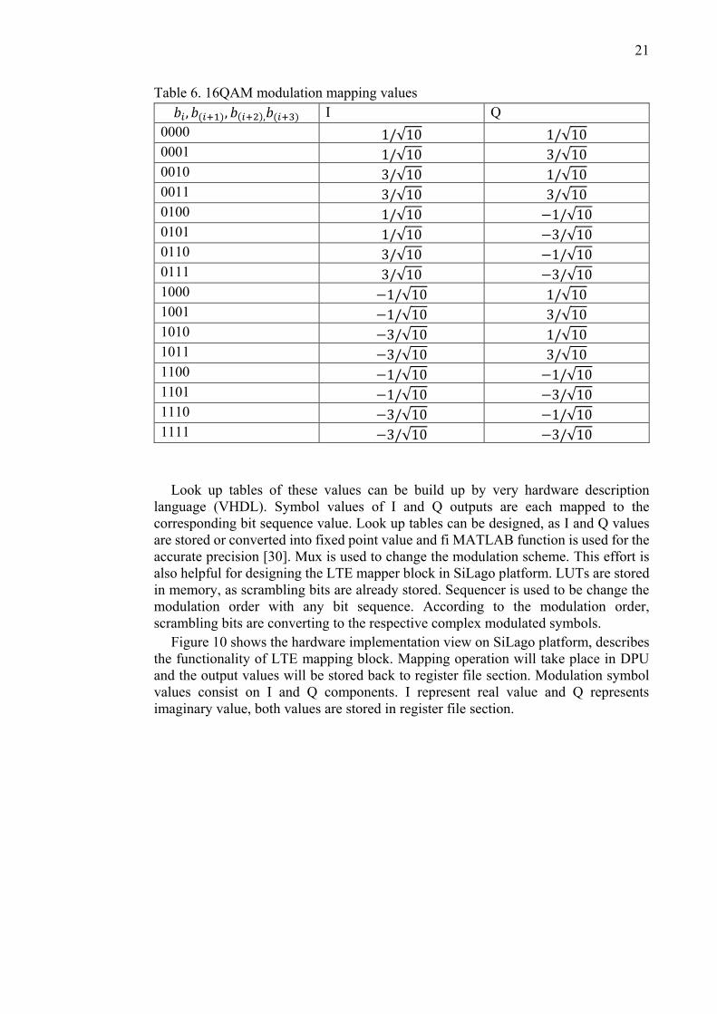
Look up tables of these values can be build up by very hardware description
language (VHDL). Symbol values of I and Q outputs are each mapped to the
corresponding bit sequence value. Look up tables can be designed, as I and Q values
are stored or converted into fixed point value and fi MATLAB function is used for the
accurate precision [30]. Mux is used to change the modulation scheme. This effort is
also helpful for designing the LTE mapper block in SiLago platform. LUTs are stored
in memory, as scrambling bits are already stored. Sequencer is used to be change the
modulation order with any bit sequence. According to the modulation order,
scrambling bits are converting to the respective complex modulated symbols.
Figure 10 shows the hardware implementation view on SiLago platform, describes
the functionality of LTE mapping block. Mapping operation will take place in DPU
and the output values will be stored back to register file section. Modulation symbol
values consist on I and Q components. I represent real value and Q represents
imaginary value, both values are stored in register file section.
22
Figure 10. LTE mapper implementation.
MATLAB code is modified for SYLVA compiler, as available in Appendix 2. In
MATLAB, scrambling bits are converted to modulation symbols as depends on which
modulation scheme is used. Modulation symbols are spilt to I and Q symbols
separately and then stored back to the memory. At least 384 bits are required for
64QAM higher modulation order. Every symbol has 16-bit value each for I and Q
component. Register file has 64 elements, whereas may be there is need to store both
I and Q values in SRAM memory block for further processing. All of this procedure
is parametric, even if other modulation schemes are selected, the number of scrambling
bits are reduced, in scrambling MATLAB section.

23
Table 7. 64QAM modulation values
𝑏𝑖 − 𝑏(𝑖+5) I Q 𝑏𝑖 − 𝑏(𝑖+5) I Q
000000 3/√42 3/√42 100000 −3/√42 3/√42
000001 3/√42 1/√42 100001 −3/√42 1/√42
000010 1/√42 3/√42 100010 −1/√42 3/√42
000011 1/√42 1/√42 100011 −1/√42 1/√42
000100 3/√42 5/√42 100100 −3/√42 5/√42
000101 3/√42 7/√42 100101 −3/√42 7/√42
000110 1/√42 5/√42 100110 −1/√42 5/√42
000111 1/√42 7/√42 100111 −1/√42 7/√42
001000 5/√42 3/√42 101000 −5/√42 3/√42
001001 5/√42 1/√42 101001 −5/√42 1/√42
001010 7/√42 3/√42 101010 −7/√42 3/√42
001011 7/√42 1/√42 101011 −7/√42 1/√42
001100 5/√42 5/√42 101100 −5/√42 5/√42
001101 5/√42 7/√42 101101 −5/√42 7/√42
001110 7/√42 5/√42 101110 −7/√42 5/√42
001111 7/√42 7/√42 101111 −7/√42 7/√42
010000 3/√42 −3/√42 110000 −3/√42 −3/√42
010001 3/√42 −1/√42 110001 −3/√42 −1/√42
010010 1/√42 −3/√42 110010 −1/√42 −3/√42
010011 1/√42 −1/√42 110011 −1/√42 −1/√42
010100 3/√42 −5/√42 110100 −3/√42 −5/√42
010101 3/√42 −7/√42 110101 −3/√42 −7/√42
010110 1/√42 −5/√42 110110 −1/√42 −5/√42
010111 1/√42 −7/√42 110111 −1/√42 −7/√42
011000 5/√42 −3/√42 111000 −5/√42 −3/√42
011001 5/√42 −1/√42 111001 −5/√42 −1/√42
011010 7/√42 −3/√42 111010 −7/√42 −3/√42
011011 7/√42 −1/√42 111011 −7/√42 −1/√42
011100 5/√42 −5/√42 111100 −5/√42 −5/√42
011101 5/√42 −7/√42 111101 −5/√42 −7/√42
011110 7/√42 −5/√42 111110 −7/√42 −5/√42
011111 7/√42 −7/√42 111111 −7/√42 −7/√42

24
4. MIMO
This chapter describes the overview of MIMO implementation techniques on
transmission side. In general, two signal processing blocks are used for the MIMO
implementation. Section 1 is deals with the general description of MIMO system and
the next two sections are covered the layer mapping and precoding signal processing
blocks respectively.
4.1. General Description
Multiple input and multiple output is an antenna mapping technique. This technique is used more than one antenna for the transmission and reception of data. High throughput and maximum spectral efficiency is utilized by MIMO. MIMO method is maximized the signal to noise ratio, increases the data rates and provides the directional beams by exploiting different techniques such as transmit diversity, spatial multiplexing and beamforming respectively [11]. [11]
Every transmitted subcarrier is multiplied with the channel matrix before the
transmission take place on transmitter side as shown in Figure 11, this channel matrix
is selected according to the MIMO modes.
Figure 11. Representation of general block diagram of MIMO system.
Different MIMO transmission modes are available in LTE. These modes have
different specifications from implementation perspective as described in Table 8 [13].
Table 8. LTE transmission modes
Mode Detail of transmission modes
Mode 1 Single antenna transmission
Mode 2 Transmit diversity
Mode 3 Open loop spatial multiplexing with cyclic delay diversity (CDD)
Mode 4 Closed loop spatial multiplexing
Mode 5 Multi user MIMO
Mode 6 Close loop spatial multiplexing using single transmission layer
Mode 7 Non-codebook based precoding utilizes single layer beam forming
Mode 8 Non-codebook based precoding utilized dual layer beam forming
Mode 9 Non-codebook based precoding supporting up to eight layers

25
In signal processing chain two blocks are related to the MIMO implementation on
transmitter side as shown in Figure 12. Layer mapper is used to mapped the modulated
symbols into different layers and in precoding section the matrix is multiplied to the
layered modulated symbols.
Figure 12. MIMO block representation.
The detail of these blocks describes in next sections, and on the other hand this
detail provides a general overview of that how the MIMO implementation take place
on hardware side from transmitter’s perspective.
4.2. Layer Mapping
All stored modulated symbols are divided into different layers before precoding block
in MIMO section. For this procedure layer mapper is used in signal processing chain.
Each code word is mapped onto one or more layers; it depends on which MIMO
mode is use. Specific instructions are given in [14]. Complex values modulated
symbols are represented by
𝑥(𝑖) = [𝑥(0)(𝑖) … 𝑥(𝑣−1)(𝑖)] 𝑇. (4.1)
The equation represents the layer mapper output, where as 𝑖 = 0,1 … , 𝑀𝑠𝑦𝑚𝑏𝑙𝑎𝑦𝑒𝑟
− 1
and v is the number of layers and 𝑀𝑠𝑦𝑚𝑏𝑙𝑎𝑦𝑒𝑟
is the number of modulated symbols per layer
[14].
In single antenna port case, there is only one layer is needed. It means, there is no
need to divide the modulated symbols and layer mapper block, prior to precoding.
In transmit diversity mode, there are two and four layers are used. The number of
layers depends upon the number of transmit antennas e.g. for two antennas, two layers
are used and same as, for four antennas, four layers are used. Moreover, in this mode
only one code word is used and Table 9 presents the code word to layer mapping for
transmit diversity [14].

26
Table 9. Layer mapping for transmit diversity
Number of Layers Number of code words Layer mapping
2 1 𝑥(0)(𝑖) = 𝑑(0)(2𝑖)
𝑥(1)(𝑖) = 𝑑(0)(2𝑖 + 1)
4 1 𝑥(0)(𝑖) = 𝑑(0)(4𝑖)
𝑥(1)(𝑖) = 𝑑(0)(4𝑖 + 1)
𝑥(2)(𝑖) = 𝑑(0)(4𝑖 + 2)
𝑥(3)(𝑖) = 𝑑(0)(4𝑖 + 3)
In spatial multiplexing case, up to eight layers are used, which should be less than
or equal to the number of antennas. One or two number of code words are also used in
spatial multiplexing. There are total 11 different cases are in consideration for the
spatial multiplexing, as for up to four layers either one or two code words are used, but
from five to eight layers two code words are used. Table 10 only described as the
different cases of layer mapping for the spatial multiplexing and mapping details for
each case is available in Table 6.3.3.2-1 in Section 6.3.3.2 in [14].
Table 10. Case description for code words to layer mapping for Spatial Multiplexing.
Case Number of Layers Number of code words
1 1 1
2 2 1
3 2 2
4 3 1
5 3 2
6 4 1
7 4 2
8 5 2
9 6 2
10 7 2
11 8 2
Implementation Analysis
In general, modulated data can be divided into layers on MATLAB, for this procedure
original code is given in [13]. Where two code words can be used to get the output,
which is equal to the 2D matrix and second dimension represents the number of layers.
[13]
But in our case, first we decide that which MIMO scheme should we use, to check
out the complexity and storage capability on our platform. In that scenario, we decided
to implement the spatial multiplexing case 7 according to our assumption as mention
in Table 10. This case divides the data stream of two code words into four layers. As
well as this case also covers the transmit diversity mode and most of the generic part

27
of spatial multiplexing from implementation perspective. According to LTE 3GPP
standard the detail for this implementation is given below in Table 11 [14].
Table 11. Spatial multiplexing implementation parameters for Layer Mapping.
Case Number of Layers Number of code Words Layer Mapping
7 4 2 𝑥(0)(𝑖) = 𝑑(0)(2𝑖)
𝑥(1)(𝑖) = 𝑑(0)(2𝑖 + 1)
𝑥(2)(𝑖) = 𝑑(1)(2𝑖)
𝑥(3)(𝑖) = 𝑑(1)(2𝑖 + 1)
Equations 4.2 to 4.5 represented the operation on code words in layer mapping as
𝑥(0)(𝑖) = 𝑑(0)(2𝑖) (4.2)
𝑥(1)(𝑖) = 𝑑(0)(2𝑖 + 1) (4.3)
𝑥(2)(𝑖) = 𝑑(1)(2𝑖) (4.4)
𝑥(3)(𝑖) = 𝑑(1)(2𝑖 + 1) (4.5)
where 𝑥(0) … 𝑥(3) are layers, 𝑑(0) is the modulated symbols of first code word,
𝑑(1) is the modulated symbols of second code word, 𝑖 = 0,1 … , 𝑀𝑠𝑦𝑚𝑏𝑙𝑎𝑦𝑒𝑟
− 1 and
𝑀𝑠𝑦𝑚𝑏𝑙𝑎𝑦𝑒𝑟
= 𝑀𝑠𝑦𝑚𝑏(0)
/2 = 𝑀𝑠𝑦𝑚𝑏(1)
/2.
MATLAB code is given in Appendix 3 as for the layer mapping of that case.
Modulated data is coming from two LTE mappers. This data is then divides into four
layers as according to above equations. But on hardware implementation side, I and Q
modulated symbols are stored separately, hence layer mapper implementation also
happens separately on these modulated symbols. Layer mapper output is stored back
to the SRAM memory, for further proceeding. If there is no need to store the mapped
layer data, it could be used directly for matrix multiplication in precoding block. This
code is only referring to the spatial multiplexing with two code words and four number
of layers.
For the proof of concept, implementation is taken place only for this case for spatial
multiplexing but the implementation of the other cases is also possible both for
transmit diversity and spatial multiplexing.
4.3. Precoding
Next procedure in MIMO block, a predefined matrix is multiplied with the stored layer
data block, according to the 3GPP specifications [14]. In precoding block section, final
output data is obtained from precoding block for the transmission on different antenna
ports. A vector of layer block data is inserted into the precoder block, where output is
generated, which is based upon, which MIMO scheme is going to be use for the
transmission. Layer block data vector is represented with the Equation 4.1 and output
from precoder block is represents with Equation 4.6 [14] as
𝑦(𝑖) = [… 𝑦(𝑝)(𝑖) … ]𝑇. (4.6)
28
Where 𝑖 = 0,1, … , 𝑀𝑠𝑦𝑚𝑏𝑎𝑝
− 1 generated block of vectors is mapped onto
resources on each antenna port, 𝑀𝑠𝑦𝑚𝑏𝑎𝑝
number of symbols per antenna port and
𝑦(𝑝)(𝑖) is signal for antenna port p.
For the transmission on single antenna port, there is no need to multiplication of
precoding matrix, but modulated symbols vector is directly used to mapped on relevant
antenna port as described in Section 6.3.4.1 in [14].
Moreover, for transmit diversity case, precoding matrix is defined according to
3GPP specification in each antenna port case e.g. two port and four port. This
precoding matrix is multiplied with layer data and transmitted on respective antenna
port. Precoding matrix specifications are available in Section 6.3.4.3 in [14].
Finally, in case of spatial multiplexing there is also a need for the multiplication of
precoder matrix with layer block data in precoding block section. This precoding
matrix is based upon the codebook. This codebook index has different matrix values
for different antenna ports configuration, as in spatial multiplexing either two or four
antenna ports can be used. For two antennas ports the codebook value is specified in
Table 6.3.4.2.3-1 in [14].
In general, for the four antenna ports, precoding matrix with code book index is
represented with 𝑊𝑛 and this equal to the Equation 4.7 as
𝑊𝑛 = 𝐼 − 2𝑢𝑛𝑢𝑛𝐻/𝑢𝑛
𝐻𝑢𝑛. (4.7)
Where I represent the identity matrix and vector 𝑢𝑛 is given in Table 6.3.4.2.3-2 in
[14]. Precoding matrix is represented with other quantity set {S} as 𝑊𝑛{𝑆}
, which
means that output columns of precoding matrix are interchanged according to the
specified values in set {S}. All values for precoding matrix for four antenna ports in
spatial multiplexing are given in Table 6.3.4.2.3-2 in detail [14].
Spatial multiplexing is divides into two types as, one is without cyclic delay
diversity closed loop precoding method and the other is with large cyclic delay
diversity open loop precoding method. In both cases precoding matrix 𝑊(𝑖) is
multiplied with layer data and the values of precoding matrix are same. The difference
is, in case of without cyclic delay diversity, precoding matrix is directly multiplied
with layer data but in case of with cyclic delay diversity, two more matrices are
multiplied with layer data as well. Description and values of matrices are given in
Section 6.3.4.2.1 and 6.3.4.2.2 in [14].
Implementation Analysis
In general, for the implementation of precoding block, usually a matrix multiplication
is done with layer block data, as either its transmit diversity MIMO mode or spatial
multiplexing.
As far as spatial multiplexing is concerned, original MATLAB codes are available
in [13], one for the generation of precoding matrix and the other one is matrix
multiplication with layer data.
29
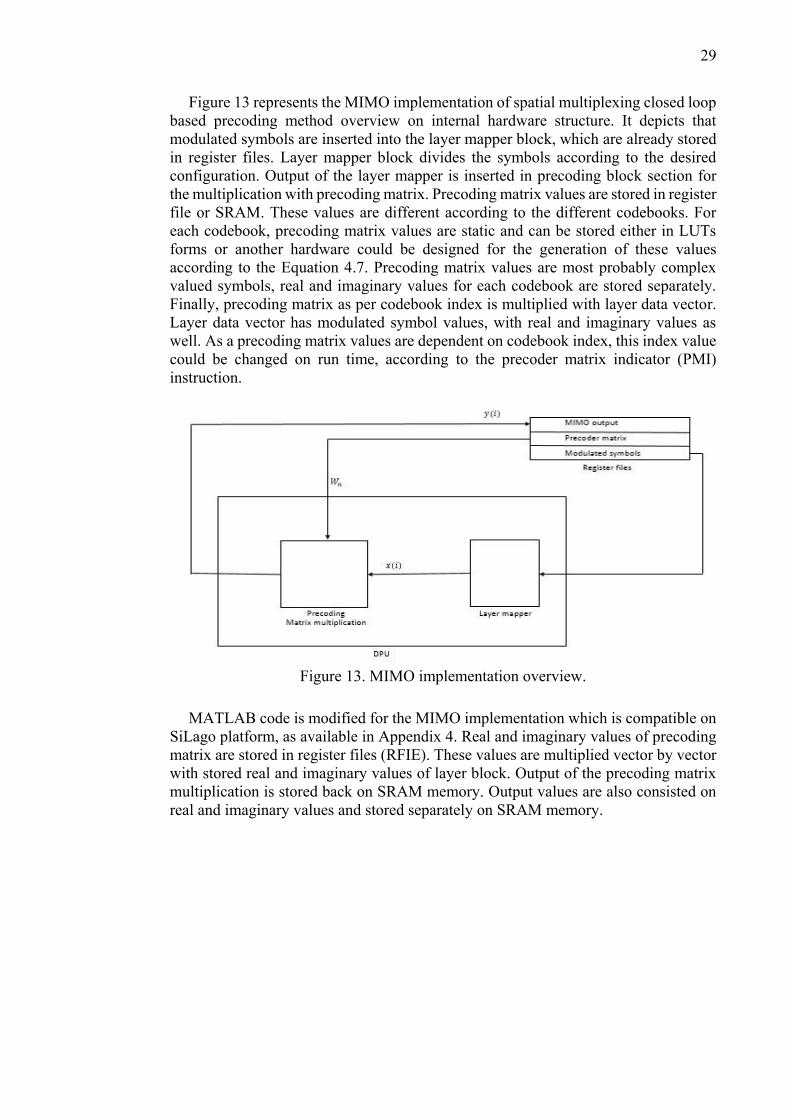
Figure 13 represents the MIMO implementation of spatial multiplexing closed loop
based precoding method overview on internal hardware structure. It depicts that
modulated symbols are inserted into the layer mapper block, which are already stored
in register files. Layer mapper block divides the symbols according to the desired
configuration. Output of the layer mapper is inserted in precoding block section for
the multiplication with precoding matrix. Precoding matrix values are stored in register
file or SRAM. These values are different according to the different codebooks. For
each codebook, precoding matrix values are static and can be stored either in LUTs
forms or another hardware could be designed for the generation of these values
according to the Equation 4.7. Precoding matrix values are most probably complex
valued symbols, real and imaginary values for each codebook are stored separately.
Finally, precoding matrix as per codebook index is multiplied with layer data vector.
Layer data vector has modulated symbol values, with real and imaginary values as
well. As a precoding matrix values are dependent on codebook index, this index value
could be changed on run time, according to the precoder matrix indicator (PMI)
instruction.
Figure 13. MIMO implementation overview.
MATLAB code is modified for the MIMO implementation which is compatible on
SiLago platform, as available in Appendix 4. Real and imaginary values of precoding
matrix are stored in register files (RFIE). These values are multiplied vector by vector
with stored real and imaginary values of layer block. Output of the precoding matrix
multiplication is stored back on SRAM memory. Output values are also consisted on
real and imaginary values and stored separately on SRAM memory.

30
5. OFDM
This chapter describes the air interface of LTE which known as OFDM in downlink
side. First section is dealt with the description of OFDM system while SCFDM is not
explained here because this air interface system is used in LTE uplink side. Second
section describes the detail of the OFDM frame structure and its possible
implementation methodology. In final section the OFDM signal generation’s
description is provided from the implementations perspective.
5.1. Definition
Orthogonal frequency division multiplexing is a type of multi carrier transmission. In
this scheme, data is transmitted over the narrowband subcarriers. It means that data is
firstly divides and transmitted onto those subcarriers, which have smaller frequency
range transmission instead of the large frequency range. This concept is useful for the
successful data transmission against the different type of interferences e.g. frequency
selective fading, ISI etc. On the other hand, these narrowband subcarriers are
multiplexed with each other and transmitted over the efficient bandwidth as illustrate
in Figure 14, orthogonality between subcarriers prevents them from the internal
interference with each other. [31]
Figure 14. Efficient Bandwidth utilization with OFDM vs FDM.
Since OFDMA has already been successfully implemented on different digital
communications applications such as digital video broadcasting, digital subscriber line
and has been the part of many standards, as theoretical and conceptual detail analysis
is available in [32]. Moreover, this scheme has also been adopted by the 3GPP LTE
due to its diverse advantages, a detail survey is available in [33].
31
Mathematical expression for the OFDM baseband signal can be expressed as from
[11]. Δ𝑓 is the subcarrier spacing and Δ𝑓 = 1/𝑇𝑢 whereas 𝑇𝑢 is equal to the modulation
symbol rate of respective subcarrier.
This Equation as explains the overall structure of OFDM baseband signal as
𝑥(𝑡) = ∑ 𝑥𝑘(𝑡)
𝑁𝑐−1
𝑘=1
= ∑ 𝑎𝑘(𝑚)
𝑁𝑐−1
𝑘=1
𝑒𝑗2𝜋𝑘Δ𝑓𝑡. (5.1)
Whereas 𝑥(𝑡) belongs to the time interval 𝑚𝑇𝑢 ≤ 𝑡 < (𝑚 + 1)𝑇𝑢, 𝑁𝑐 is represents
the number of subcarriers, 𝑘 is the index of modulated subcarrier 𝑥𝑘(𝑡) with frequency
𝑓𝑘 = 𝑘. Δ𝑓 and 𝑎𝑘(𝑚) is the complex modulation symbol during the 𝑚𝑡ℎ OFDM
symbol interval [11].
One important point is that; all subcarriers holds the complex modulated symbols
which represents with 𝑎𝑘 in frequency domain and when IFFT is implemented on these
subcarriers after that an OFDM symbol is generated in time domain which holds many
modulated subcarriers in frequency domain and the Equation (5.1) is basically explains
a general model of any subcarrier modulated symbol as in accordance with respective
OFDM symbol interval.
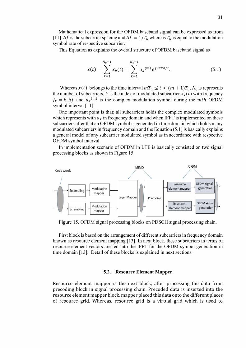
In implementation scenario of OFDM in LTE is basically consisted on two signal
processing blocks as shown in Figure 15.
Figure 15. OFDM signal processing blocks on PDSCH signal processing chain.
First block is based on the arrangement of different subcarriers in frequency domain
known as resource element mapping [13]. In next block, these subcarriers in terms of
resource element vectors are fed into the IFFT for the OFDM symbol generation in
time domain [13]. Detail of these blocks is explained in next sections.
5.2. Resource Element Mapper
Resource element mapper is the next block, after processing the data from precoding block in signal processing chain. Precoded data is inserted into the resource element mapper block, mapper placed this data onto the different places of resource grid. Whereas, resource grid is a virtual grid which is used to

32
understand the arrangement of data, later on this arranged data is inserted into the IFFT for the OFDM signal generation [13].
In other words, resource grid is generated from the resource element mapper, as by
placing the data which comes from different channels onto the relevant places on the
resource grid. For mapping this data on resource grid, it is quite necessary to
understand all parameters which are used in resource grid. Usually resource grid is
based upon the frequency and time domain structure from the understanding
perspective. Some of the instructions in order to arrange the data onto the resource grid
are quite same, others are different according to the specifications. In resource element
mapper, different type of data comes from different channels from higher layers and
some of the signals are generated separately, also fed into the resource element
mapper. Resource element mapper takes all data and mapped it on to the resource grid.
[11, 14, 10]
Data is extracted from these channels to be mapped on to the resource grid as,
Physical downlink shared channel (PDSCH)
Physical multicast channels (PMCH)
Physical broadcast channel (PBCH)
Primary synchronization signals (PSS)
Secondary synchronization signals (SSS)
Reference signals (RS)
Physical downlink control channels (PDCCH)
Physical control format indicator channel (PCFICH)
Physical hybrid automatic repeat request indicator channel (PHICH)
User data is associated with PDSCH. PMCH is used for the multimedia broadcast
single frequency network (MBSFN). PBCH is used for the system information to help
out the terminal for cell search. In general PSS, SSS and RS are used to
synchronization and equalization purpose on receiver side, these signals are generated
separately according to the LTE specifications and not associated with higher layers.
PDCCH, PCFICH, PHICH are control channels, also known as L1/L2 control channels
and moreover PDCCH has linked with downlink control information (DCI) formats.
The data of all channels are inserted on to the resource grid; the places are arranged
by the resource element mapper. Resource grid is based upon the LTE frame structure,
as frame structure is either frequency division duplexing (FDD) or time division
duplexing (TDD) type. Figure 16 represents FDD frame structure’s generic overview
from the time domain’s perspective, as which shows that every frame has a 10ms long
duration in time, whereas each sub frame has a 1ms long, which means that each frame
is consisted on 10 sub frames. Furthermore, each sub frame is consisted on 2 time slots
and each time slot has a 0.5ms duration in time domain. One-time slot is consisted on
either 7 or 6 OFDM symbols, depends on CP types as normal CP or extended CP
respectively.

33
Figure 16. Generic Overview of LTE time domain FDD frame structure.
From frequency domain’s perspective, each OFDM symbol is consisted on different
number of OFDM subcarriers as according to the bandwidth. In general, resource grid
is presented with resource block and this resource block is associated with one-time
slot. Each resource block has 12 OFDM subcarriers on y-axis in frequency domain and
6 or 7 OFDM symbols on x-axis in time domain, as depicts in Figure 17. Each element
in resource block is known as resource element which is the smallest unit in entire
resource grid. Resource element is filled with one complex modulated symbol by the
resource element mapper and known as OFDM sub carrier.
Figure 17. LTE Resource Grid.

34
This resource block is known as a resource grid for FDD frame structure and whole
data is mapped directly to the resource block. Number of resource blocks are
associated with the transmitted bandwidth. All resource blocks respective to their
specified bandwidth are presented within one-time slot, whereas 6 or 7 OFDM
symbols are remain same in x axis but number of subcarriers are increases according
to the bandwidth on y axis. The arrangement of resource blocks as shown in Figure 18
for 1.4MHz bandwidth which has 72 sub carriers and 6 resource blocks. And for other
bandwidths, resource blocks are arranged in the same way.
Figure 18. Resource Block arrangement in 1.4MHz BW.
Table 11 [34, 35] shows the number of resource blocks and number of subcarriers
according to the LTE bandwidth specifications. These parameters are important to
understand for the implementation perspective.
Table 11. Number of Resource blocks according to LTE bandwidth
Bandwidth(MHz) Number of Resource Blocks Number of Subcarriers
1.4 6 72
3 15 180
5 25 300
10 50 600
15 75 900
20 100 1200

35
Implementation Analysis
According to the 3GPP standard the data is mapped to the resource grid with index
pair (k, l) which represents the one resource element where 𝑘 = 0, … , 𝑁𝑅𝐵𝐷𝐿𝑁𝑆𝐶
𝑅𝐵 − 1 is
the resource element value in frequency domain and 𝑙 = 0, … , 𝑁𝑆𝑦𝑚𝑏𝐷𝐿 − 1 is the
resource element value in time domain.
Five different types of reference signals are used in LTE downlink side and these
reference signals are transmitted according to the specified antenna ports, the detail of
generation and mapping the reference signals on different antenna ports are given in
Section 6.10 in [14]. Usually, cell specific reference signals are used for the
transmission, which are associated with the PDSCH. Cell specific reference signals
are transmitted on 0 to 3 antenna ports. The arrangements of these reference signals in
each resource block is taken place separately, for different antenna ports. For
synchronization signals, generation and mapping details are available in Section 6.11
in [14]. Whereas these signals are generated with Zadoff-Chu sequences [14]. In FDD
frame structure, both PSS and SSS are available in each first slot of sub-frame 0 and 5
at the last and second last OFDM symbol respectively. Control channels are available
usually at first OFDM symbol and resource element groups are introduced for the
mapping of these signals according to 3GPP, mapping detail is available in Section
6.2.4 in [14]. PBCH are available in first sub-frame of each radio frame and the detail
of mapping is available in Section 6.6.4 in [14]. Whereas PDSCH data is mapped on
other OFDM symbol as mentioned in Section 6.3.5 in [14].
In real implementation scenario, the data is mapped on frequency domain side, by
the correct arrangement as according to the specifications. Data should be arranged by
considering the first OFDM symbol specifications with first slot number as with first
sub-frame in every radio frame. For example, if the bandwidth is 1.4 MHz, 6 resource
blocks with 72 subcarriers are included in first OFDM symbol. Data should be
arranged as starts from first slot number and with first OFDM symbol then second
OFDM symbol mapping will be considered with another 72 subcarriers arrangement
with respective arrangement specification and this process will be continued. Later on,
the first OFDM symbol supposition arrangement which consists of 72 OFDM
subcarriers whereas in real senses each subcarrier is consists on complex modulated
symbol. It means for real and imaginary part, there will be a parallel arrangement is
needed for each subcarrier, finally this arrangement is inserted to the IFFT for real
OFDM symbol generation.
MATLAB code is given for the implementation of resource grid in [13]. Whereas
only cell specific reference signals and user data is considered for the generation of
resource grid. Three main entities are under consideration for mapping the data as one
is number of subcarriers, second is the slot number and third is sub frame number. The
indexes of these entities are used for mapping the data onto the resource grid.
In our case, we just only considered the PDSCH data as which already stored in
memory and it could be arranged by resource element mapper or directly inserted into
the IFFT block.

36
5.3. OFDM Signal Generation
After the arrangements of modulated data with resource element mapper, the data is
fed into the IFFT block. IFFT is operated on each column or OFDM symbol of
resource grid which consists on different number of subcarriers as according to the
Table 11. This FFT/IFFT is also different in sizes according to the LTE specified
bandwidth describes in Table 12 [34, 35]. According to that table respective size of
FFT/IFFT is used. FFT/IFFT is implemented with fast fourier transform algorithm
which developed by Cooley and Tukey [36].
Table 12. LTE FFT size according to respective bandwidth
Bandwidth(MHz) Sampling Frequency(MHz) FFT size
1.4 1.92 128
3 3.84 256
5 7.68 512
10 15.36 1024
15 23.04 1536
20 30.72 2048
From implementation perspective, the vector of subcarriers is taken from the
resource element mapper and appended zeros by zero padding block before the
insertion to the FFT/IFFT section. Zeros are padded at direct current (DC) subcarrier
and around the edges of DC subcarrier [37], until the numbers of subcarriers required
for FFT/IFFT size are achieved. After the FFT/IFFT section cyclic prefix is inserted
to the OFDM time domain symbol. Cyclic prefix is used as a guard interval provided
to the OFDM symbols. Two type of cyclic prefix are used one is known as normal
cyclic prefix and the other known as extended cyclic prefix. [13]
For implementation perspective FFT/IFFT is already developed for SiLago
platform as in [18] and we just need to inserts the data to the MATLAB code which is
also designed and available for the FFT/IFFT functionality. CP implementation is out
of scope at this time.

37
6. RESULTS
Two parts are considered for the results section. One part consists of the development
of MATLAB codes for SiLago platform. These codes are modified version of already
available golden model of MATLAB functions in [20]. The developed MATLAB
codes are in generally arranged in the manner of SYLVA compiler. The modifications
are made according to the compilers instruction. In these codes, real and imaginary
data is divided for the implementation on SiLago platform.
After the development of these codes when input is inserted in MATLAB original
codes and the modified version codes, the output is same. Later on, these MATLAB
codes are useful for the high-level synthesis of considered signal processing blocks on
SiLago platform.
In the other part of results section, the assumptions of three models with different
specifications are considered and modeled it on MATLAB as available in Table 13.
Table 13. Assumptions for modeling
Case Number of bits Modulation FFT size
1 1200 QPSK 512
2 4800 QAM-16 1024
3 14400 QAM-64 2048
In first part, we designed the modeling library on Simulink for considered signal
processing blocks as shown in Figure 19. In this library, we have assigned the
parameter values according to our assumptions which are mapped directly on SiLago
platform.
Figure 19. LTE model Simulink Library.
For this purpose, meanwhile we have also updated the lib file for the results
generation on the basis of these parameters, this lib file is also available in Appendix
5 and different functional implementations are also presents for the more
computational complex blocks for example in precoding and FFT section.
After that on the basis of this library three systems are interconnected on Simulink
on the behalf of this library which represents the three-different cases.
Figure 20 represents the first case of our assumptions. We have considered two
code words and 1200 scrambler bits input.

38
Figure 20. QPSK PDSCH processing Simulink blocks.
QPSK scheme is considered as a modulated implementation part. Layer mapper
divides the symbols into four independent streams. In precoding section a matrix is
multiplied with layer mapper symbols. Resource element mapper is just passed
through the four streams towards the IFFT block. In IFFT section 512 FFT size is
implemented. Four frequency domain streams are converted into the time domain
streams. Time domain streams are ready to be inserted into digital front end processing
part of transmitter. After the analog domain these four streams data are out from four
different antennas.
Figure 21 represents the synchronous data flow graph for the insertion of our
models into the SiLago platform.
Figure 21. Synchronous data flow graph for modeling.
Moreover, synthesis result values are present in Table 14 for case 1.
Table 14. Synthesis results for QPSK mode
FIMPS Area
(SiLago Cells)
Latency
(Cycles)
Sample Interval
22 49 5523 2398
Table 14 represents the implementation results of QPSK modeling blocks on
SiLago platform using the system level synthesis tool, called Sylva [17]. Sylva
evaluated 22 different functions (FIMP in Table 14). The total area consumed by in
terms of SiLago blocks was 49. i.e. 49 was the optimal number of SiLago cells to
implement the LTE transmitter taking into consideration the design constraints. Sylva
synthesized the design on 400 MHz clock frequency. The first output from the

39
transmitter took a latency of 5523 cycles. After filling the pipeline, the design was able
to generate an output after every 2398 cycles (referred to as sample interval in the
Table 14).
Figure 21 shows the second case of modeling blocks on our assumption. In this case
4800 bits are used in scrambler part.
Figure 21. QAM-16 PDSCH Simulink blocks.
QAM 16 is considered for the modulated implementation part. At the end 1024
point FFT size is used for the IFFT implementation. The data flow procedure is same
from implementation scenario as mentioned in case 1.
Table 15 represents the synthesis results of QAM-16 mode. According to these
results Sylva evaluates the 20 different functions.
Table 15. Synthesis results for QAM-16 mode
FIMPs Area
(SiLago Cells)
Latency
(Cycles)
Sample Interval
20 47 15951 9598
The total area is consumed by in terms of SiLago blocks was 47. In this
implementation, the first output comes from transmitter took a latency of 15951 cycles.
After the filling of pipeline, this design was able to generate an output after every 9598
intervals.
The final assumptions are taken place in case 3 as shown in Figure 22. Whereas
14400 bits are used as in scrambler part. QAM-64 is used for the mapping scheme as
in modulation part. In IFFT block 2048 point FFT is considered for the IFFT
implementation. The data flow procedure is same as mentioned in above cases.
Figure 22. QAM-64 PDSCH Simulink blocks.

40
Table 16 shows the synthesis results for QAM-64 mode as a case 3 on SiLago
platform. Sylva evaluates the 24 different functions (FIMP in Table 16).
Table 16. Synthesis results for QAM-64 mode
FIMPS Area
(SiLago Cells)
Latency
(Cycles)
Sample Interval
24 51 42553 28798
The total area consumed by in terms of SiLago blocks was 51. i.e. 51 was the
optimal number of SiLago cells to implement the LTE transmitter taking into
consideration the design constraints. As already mentioned above, Sylva synthesized
the design on 400 MHz clock frequency. The first output from the transmitter took a
latency of 42553 cycles. After filling the pipeline, the design was able to generate an
output after every 28798 cycles (referred to as sample interval in the Table 16).
In Figure 23 chart shows the comparison between three different cases with the
normalization factor of synthesis results. This chart depicts that case 3 is one of the
more resource hungry part on SiLago platform. It means that FIMPs, area, latency and
sample intervals are huge in case 3 as in comparison to case 2 and case 1. While in
case 2 the number of FIMPs and area are slightly less as compared to the case 1. But
latency and sample intervals are greater in case 2 than in case 1.
Figure 23. Normalization chart of synthesis result.
0
0,2
0,4
0,6
0,8
1
1,2
FIMPs Area Latency Sample Interval
Normalization of synthesis result
Case1 Case2 Case3

41
7. DISCUSSION
In this master thesis, we have implemented the PDSCH base band signal processing
blocks on the SiLago platform from high level synthesis perspective. For this purpose,
we have theoretically studied about these blocks. Scrambler, mapper, MIMO and
OFDM blocks are studied from LTE standards perspective. LTE scrambler consists on
the two LFSR. One LFSR initial condition is given but the other LFSR initial condition
is parametric which is based upon LTE radio resource scheduling scheme. This scheme
is also discussed in this thesis for the LTE scrambler part. LTE mapper block depends
on the three modulation schemes namely as QPSK, 16-QAM and 64-QAM. The
implementation technique of these modulation schemes for SiLago platform is also
presented in this thesis. MIMO signal processing block which is based on further two
signal processing blocks as layer mapper and precoding block, also explained in detail
in this thesis. While OFDM block consists on the resource element mapper and OFDM
signal generation block. In resource element mapper section the detail of different LTE
channels and its implementation scenario is discussed. And in OFDM signal
generation block the explanation is presented relating to how the modulated data is
inserts from resource element block to the IFFT block.
SiLago platform is based upon the two-coarse grain reconfigurable architectures
and the behaviour of SiLago platform is considered as a high-level synthesis
perspective. The detail of SiLago platform and its design methodology is also
explained in this thesis.
We have done analysis of considered signal processing blocks for the
implementation scenario on the SiLago platform. We have developed the MATLAB
codes for the SiLago platform. The codes are based upon the SYLVA compilers
instructions. Real and imaginary data is also divides in these codes. On the other hand,
we have also managed the data flow on architectural level. The data flow is managed
in terms of register files and SRAM. Three different modes of these blocks are
considered for the implementation on SiLago platform that is why three different types
of data flow is managed. At the end, we have modeled considered signal processing
blocks on Simulink. The blocks are used for SYLVA compiler after that we present
the results in terms of area, latency, functional implementations and time interval,
generated with the help of the SYLVA tool.
We have found that the dynamic behaviour of these blocks is a challenge to
implement on SiLago platform. The Sylva compiler is not able to switch one
functionality to the other on runtime. For example, in our case it is not possible yet
that Sylva tool switch QPSK to QAM-16 or QAM-64 on run time. That is why we
have developed three different cases on our platform.
From future perspective, we will try to implement the receiver side signal
processing blocks of LTE on SiLago platform. We will also need to improve the
dynamic behaviour of SiLago platform in future. In other terms the implementation of
radio resource management of LTE on SiLago platform is the next challenge.
42
8. SUMMARY
Long term evolution is a latest wireless standard known as fourth generation cellular
technology which is developed by 3GPP. The base band signal processing of LTE
standard is quite complex for implementation perspective on hardware. Different
hardware platforms are used for signal processing algorithms of LTE. A newly
developed SiLago platform is introduced in this master thesis which is used the CGRA
based architecture. While SiLago platform consists on the SiLago design
methodology. SiLago design methodology depends on the three steps. While LTE
PDSCH base band signal processing blocks are considered for the implementation on
SiLago platform. PDSCH blocks are the main building blocks of LTE. Whereas LTE
scrambling, modulation, MIMO and OFDM signal processing blocks are included in
PDSCH signal processing chain.
One advantage of scrambler is the reduction of interferences in LTE. LTE scrambler
is based upon the two LFSR which are used to produce the gold sequence of bits. These
bits are exclusive or with incoming bits from the previous block of LTE signal
processing chain. After scrambling the bits, LTE mapper is used to map these bits on
three different modulation schemes. Different number of bits are mapped to the
complex modulation symbols as depends on which modulation scheme is used. For
example, in QPSK 2 bits are mapped to the complex modulated symbols same as 4
bits and 6 bits are used in QAM 16 and QAM 64 modulation schemes respectively.
After modulation of the symbols the data is inserted into the MIMO section. Two
blocks are considered for the MIMO implementation. As one is known as layer
mapping block in this block the modulated symbols are divides into different layers.
Layers division is based upon the MIMO antenna transmission scheme. In our case,
we assumed that the data is transmitted on four antennas. That is why the modulated
symbols are divides into four number of layers. While the next block of MIMO named
as precoding block deals with the complex matrix multiplication of the layered
modulated symbols. In precoding, different cases of matrix multiplication are used
which is based upon the MIMO transmission mode. As in general transmit diversity,
spatial multiplexing and beamforming is used in MIMO. In our case, we assumed the
spatial multiplexing case for four antenna transmission. For this different number of
codebook based complex matrices are used for the multiplication of layer modulated
data.
When the complex matrix multiplication of layer data is done in MIMO block then
these modulated symbols are inserted into the OFDM block. OFDM block consist on
the resource element mapper and OFDM signal generation block. In resource element
mapper, the complex modulated data which comes from previous block is arranged
with other channels data. Resource element mapper is quite complex for understanding
perspective which is based on the time frequency grid. When data is arranged in
resource element mapper then this data is ready to inserts in the OFDM signal
generation block. Where IFFT is implemented on inserted data and converts this data
from frequency domain to the time domain.
In result section three different modes are considered for the PDSCH base band
signal processing blocks. According to these modes three Simulink models are
developed. One general library is also developed for these blocks on Simulink. In
parallel the MATLAB codes are also developed for SiLago platform. The developed
models are inserted into the SYLVA compiler for results generation. SYLVA mapped

43
these models onto the SiLago platform from high level synthesis perspective. At the
end results are generated in terms of area, latency and the sample interval of SiLago
platform.

44
9. REFERENCES
[1] A. Gupta and R. K. Jha, "A Survey of 5G Network: Architecture and
Emerging Technologies," in IEEE Access, vol. 3, no. , pp. 1206-1232, 2015.
[2] J. Berkmann, C. Carbonelli, F. Dietrich, C. Drewes and W. Xu, "On 3G LTE
Terminal Implementation - Standard, Algorithms, Complexities and
Challenges," 2008 International Wireless Communications and Mobile
Computing Conference, Crete Island, 2008, pp. 970-975.
[3] P. Brauer, M. Lundqvist and A. Mällo, "Improving Latency in a Signal
Processing System on the Epiphany Architecture," 2016 24th Euromicro
International Conference on Parallel, Distributed, and Network-Based
Processing (PDP), Heraklion, 2016, pp. 796-800.
[4] Ian Kuon, Russell Tessier and Jonathan Rose (2008), "FPGA Architecture:
Survey and Challenges", Foundations and Trends® in Electronic Design
Automation: Vol. 2: No. 2, pp 135-253.
[5] R. Hartenstein, "A decade of reconfigurable computing: a visionary
retrospective," Proceedings Design, Automation and Test in Europe.
Conference and Exhibition 2001, Munich, 2001, pp. 642-649.
[6] M. A. Shami and A. Hemani, "Control Scheme for a CGRA," 2010 22nd
International Symposium on Computer Architecture and High Performance
Computing, Petropolis, 2010, pp. 17-24.
[7] Hadi Esmaeilzadeh, Emily Blem, Renee St. Amant, Karthikeyan
Sankaralingam, and Doug Burger. 2011. Dark silicon and the end of
multicore scaling. SIGARCH Comput. Archit. News 39, 3 (June 2011), 365-
376. DOI=http://dx.doi.org/10.1145/2024723.2000108
[8] S. M. A. H. Jafri et al., "Energy-aware coarse-grained reconfigurable
architectures using dynamically reconfigurable isolation cells," International
Symposium on Quality Electronic Design (ISQED), Santa Clara, CA, 2013,
pp. 104-111.
[9] N. Farahini, A. Hemani, H. Sohofi and S. Li, "Physical design aware system
level synthesis of hardware," 2015 International Conference on Embedded
Computer Systems: Architectures, Modeling, and Simulation (SAMOS),
Samos, 2015, pp. 141-148.
[10] Stefina Sesia, Issam Toufik and Matthew Beker, “LTE The UMTS Long
Term Evolution from Theory to Practise’’.
[11] Eirk Dahlman, Stefan Parkvall and Johan Skold“4G: LTE/LTE-Advanced
for Mobile Broadband”, 2014.

45
[12] T. Jiang and Y. Wu, "An Overview: Peak-to-Average Power Ratio
Reduction Techniques for OFDM Signals," in IEEE Transactions on
Broadcasting, vol. 54, no. 2, pp. 257-268, June 2008.
[13] Houman Zarrinkoub,” Understanding LTE with MATLAB from
Mathematical Modeling to Simulation and Prototyping”.
[14] 3GPP TS 36.211, Physicals Channels and Modulation, version 11.2.0,
Release 11, 2012-09.
[15] 3GPP TS 36.212, Multiplexing and Channel coding, version 12.2.0 Release
12, 2014-10.
[16] D. Wu, J. Eilert, D. Liu, A. Nilsson, E. Tell and E. Alfredsson, "System
architecture for 3GPP LTE modem using a programmable baseband
processor," 2009 International Symposium on System-on-Chip, Tampere,
2009, pp. 132-137
[17] Nasim Farahini, “SiLago: Enabling System Level Automation Methodology
to Design Custom High-Performance Computing Platform,” Doctoral
Thesis in ICT, KTH, Stockholm, Sweden 2016.
[18] M. A. Shami, “ Dynamically Reconfigurable Resource Array”, Doctoral
Thesis in ICT, KTH, Stockholm, Sweden 2012.
[19] M. A. Shami and A. Hemani, "Morphable DPU: Smart and efficient data
path for signal processing applications," 2009 IEEE Workshop on Signal
Processing Systems, Tampere, 2009, pp. 167-172.
[20] O. Malik and A. Hemani, "Synchronizing distributed state machines in a
coarse grain reconfigurable architecture," 2011 International Symposium on
System on Chip (SoC), Tampere, 2011, pp. 128-135.
[21] M. A. Shami and A. Hemani, "Address generation scheme for a coarse grain
reconfigurable architecture," ASAP 2011 - 22nd IEEE International
Conference on Application-specific Systems, Architectures and Processors,
Santa Monica, CA, 2011, pp. 17-24.
[22] M. A. Tajammul, M. A. Shami, A. Hemani and S. Moorthi, "NoC Based
Distributed Partitionable Memory System for a Coarse Grain
Reconfigurable Architecture," 2011 24th Internatioal Conference on VLSI
Design, Chennai, 2011, pp. 232-237.
[23] S. P. Azad, N. Farahini and A. Hemani, "Customization methodology of a
Coarse Grained Reconfigurable architecture," 2014 NORCHIP, Tampere,
2014, pp. 1-4.
[24] Shuo Li, N. Farahini, A. Hemani, K. Rosvall and I. Sander, "System level
synthesis of hardware for DSP applications using pre-characterized function
implementations," 2013 International Conference on Hardware/Software
46
Codesign and System Synthesis (CODES+ISSS), Montreal, QC, 2013, pp.
1-10.
[25] X. Chen, W. Yang, C. Xu and Y. I. Kim, "RNTI Allocation Schemes for
User Equipments in LTE System," 2012 8th International Conference on
Wireless Communications, Networking and Mobile Computing, Shanghai,
2012, pp. 1-4.
[26] Youngkwon Ryu and Jeong Gon Kim, "Cell search for 3GPP LTE system
using interference cancellation," 2015 Seventh International Conference on
Ubiquitous and Future Networks, Sapporo, 2015, pp. 579-584.
[27] Y. Wang, A. Abdelhadi and T. C. Clancy, "Optimal power allocation for
LTE users with different modulations," 2016 Annual IEEE Systems
Conference (SysCon), Orlando, FL, 2016, pp. 1-5.
[28] Sampath Kumar D and P. Samundiswary, "Performance analysis of MIMO-
LTE using various modulation schemes under different channels," 2015
International Conference on Electrical, Electronics, Signals,
Communication and Optimization (EESCO), Visakhapatnam, 2015, pp. 1-
4.
[29] Jakob L. Buthler and Michael Buhl, “Implementation of a LTE inspired
Transceiver On a USRP Platform,” Group12gr1056, Aalborg University,
May 2012.
[30] Online Available: https://se.mathworks.com/help/fixedpoint/ref/fi.html.
[31] Richard van Nee and Ramjee Prasad, “OFDM for Multimedia Wireless
Communications.
[32] Ahmad R.S Bahai, Burton R.Saltzberg and Mustafa Ergen, “ Mulit-Carrier
Digital Communictions Theory and Applications of OFDM” Second
Edition.
[33] T. Hwang, C. Yang, G. Wu, S. Li and G. Y. Li, "OFDM and Its Wireless
Applications: A Survey," in IEEE Transactions on Vehicular Technology,
vol. 58, no. 4, pp. 1673-1694, May 2009.
[34] 3GPP TS 36.211 V9.4.0 (2010-07), “Evolved Universal Terrestrial Radio
Access (E-UTRA); Base Station (BS) radio transmission and reception”.
[35] 3GPP TS 36.101 V8.4.0 (2008-12), “Evolved Universal Terrestrial Radio
Access (E-UTRA); User Equipment (UE) radio transmission and reception.”
[36] C. H. Yang, T. H. Yu and D. Markovic, "Power and Area Minimization of
Reconfigurable FFT Processors: A 3GPP-LTE Example," in IEEE Journal
of Solid-State Circuits, vol. 47, no. 3, pp. 757-768, March 2012.
[37] H. Kee, S. S. Bhattacharyya, I. Wong and Y. Rao, "FPGA-based design and
implementation of the 3GPP-LTE physical layer using parameterized

47
synchronous dataflow techniques," 2010 IEEE International Conference on
Acoustics, Speech and Signal Processing, Dallas, TX, 2010, pp. 1510-1513.

48
10. APPENDICES
Appendix 1. Scrambler code
Appendix 2. Mapper code
Appendix 3. Layer Mapper code
Appendix 4. MIMO code
Appendix 5. Modeling lib file

49
Appendix 1. Scrambler code
Mode=1; % M=1,2,3 then 4QAM, 16QAM, 64QAM respectively.
if Mode==1
type=1;
elseif Mode==2
type=2;
elseif Mode==3
type=4;
end
Number_of_bits=1200*Mode*type;
bits_from_scrambler=Number_of_bits;
% SRAM to declaration
M_1=[1:Number_of_bits/16]; %!MEM<0,0>;
%Memory initialiazation
M_1=randi([0 1],Number_of_bits/16,1);
reg_size=64;
reg_loop_size=64*ceil((Number_of_bits/16)/reg_size);
reg_1=[1:64];%!REFI
% LFSR_1_codition
LFSR_1_condition=[zeros(1, 30) 1]; %!REFI <0,1>
% LFSR_2_initialcondition_parameters
RNTI=1;q=0;nS=1;NcellID=0; %!REFI <0,1>
%Codeword_input= %!MEM<0,0>
for i=1:64:Number_of_bits/16
temp=min(i+63, Number_of_bits/16); %!DPU <0,0>
reg_1=M_1(i:temp);
reg_1=scrambler_DPU(reg_1, LFSR_1_condition,RNTI,q,nS,NcellID) %!
DPU<> [0,0]
M_1(i:temp)=reg_1
end

50
Appendix 2. Mapper code
register_size=64;
% Memory size
M_size_original=1024;
M_size=(bits_from_scrambler)/(2*Mode);
% Register file size
R=(bits_from_scrambler/Mode);
if Mode==1
Memory_real =[1:(M_size+40)]; %! MEM<> [1,1]
Memory_imag=[M_size+41:M_size_original]; %! MEM<>[1,1]
Memory_imag=[1:((2*(M_size+40))-M_size_original)+40]; %! MEM <>
[1,2]
elseif Mode==2
Memory_real = [1:M_size_original]; %! MEM <>[1,1]
Memory_real = [1:((M_size+16)-(M_size_original))]; %! MEM <>[1,2]
Memory_imag = [((M_size+16)-(M_size_original))+1:M_size_original];
%! MEM <> [1,3]
Memory_imag = [1:((M_size+16)-(M_size_original-((M_size+16)-
(M_size_original))))]; %! MEM <> [1,4]
elseif Mode==3
Memory_real = [1:M_size_original]; %! MEM <> [1,1]
Memory_real = [1:M_size_original]; %! MEM <> [1,2]
Memory_real = [1:((M_size+32)-(2*(M_size_original)))]; %! MEM<>
[1,3]
Memory_imag = [((M_size+32)-(2*M_size_original))+1:M_size_original];
%! MEM <> [1,3]
Memory_imag = [1:M_size_original]; %! MEM <> [1,4]
Memory_imag = [1:((M_size+32)-(M_size_original+(M_size_original-
((M_size+32)-(2*M_size_original)))))]; %! MEM <> [1,5]
end
% Register file declaration
Reg1_real=[1:register_size]; %! RFILE<> [1,1]
Reg2_imag=[1:register_size]; %! RFILE<> [1,2]
for n=1:ceil((R/2)/register_size)
Reg1_real=mapper_DPU_real(Scrambler_output,Mode,n,register_size,R,bi
ts_from_scrambler); %! DPU<> [1,1]

51
Reg2_imag=mapper_DPU_imag(Scrambler_output,Mode,n,register_size,R,bi
ts_from_scrambler); %! DPU<> [1,1]
Memory_real((n-1)*64+1:n*64)=Reg1_real;
Memory_imag((n-1)*64+1:n*64)=Reg2_imag;
end

52
Appendix 3. Layer Mapper Code
% Instruction for Layer mapper
c=2; % Number of Codewords
v=4; % Number of Layers
% comes from other mapper.
LayerMapper1_real=Memory_real; %! MEM<> [1,1]
LayerMapper2_real=Memory_real; %! MEM<> [1,1]
LayerMapper1_imag=Memory_imag; %! MEM<> [1,1]
LayerMapper2_imag=Memory_imag; %! MEM<> [1,1]
% Real layer mapping
size_real=size(LayerMapper1_real,1);
LayerMapper1_real_out=zeros(size_real/2,v);
size_imag=size(LayerMapper1_imag,1);
LayerMapper1_imag_out=zeros(size_imag/2,v);
for n=1:size_real/2
L1_real(n)=LayerMapper1_real(n*2-1);
L2_real(n)=LayerMapper1_real(n*2);
L3_real(n)=LayerMapper2_real(n*2-1);
L4_real(n)=LayerMapper2_real(n*2);
L1_imag(n)=LayerMapper1_imag(n*2-1);
L2_imag(n)=LayerMapper1_imag(n*2);
L3_imag(n)=LayerMapper2_imag(n*2-1);
L4_imag(n)=LayerMapper2_imag(n*2);
LayerMapper1_real_out(n,:)=[L1_real(n);L2_real(n);L3_real(n);L4_real
(n)]
LayerMapper1_imag_out(n,:)=[L1_imag(n);L2_imag(n);L3_imag(n);L4_imag
(n)]
end
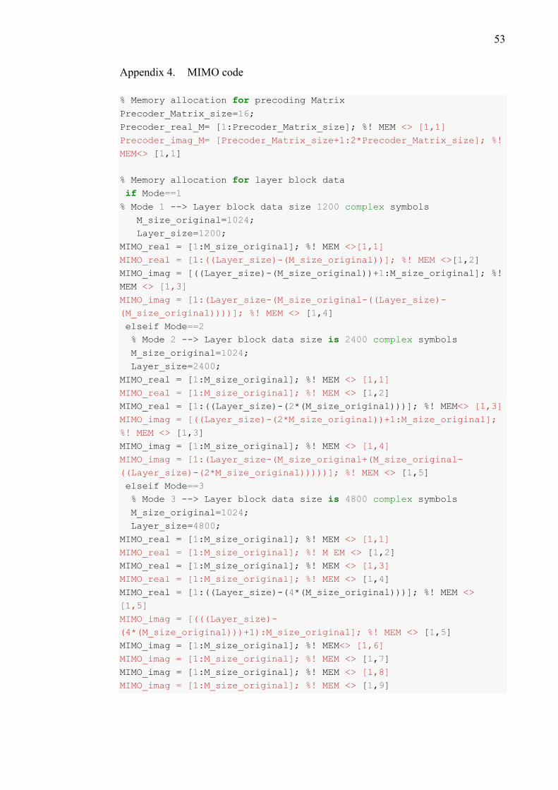
53
Appendix 4. MIMO code
% Memory allocation for precoding Matrix
Precoder_Matrix_size=16;
Precoder_real_M= [1:Precoder_Matrix_size]; %! MEM <> [1,1]
Precoder_imag_M= [Precoder_Matrix_size+1:2*Precoder_Matrix_size]; %!
MEM<> [1,1]
% Memory allocation for layer block data
if Mode==1
% Mode 1 --> Layer block data size 1200 complex symbols
M_size_original=1024;
Layer_size=1200;
MIMO_real = [1:M_size_original]; %! MEM <>[1,1]
MIMO_real = [1:((Layer_size)-(M_size_original))]; %! MEM <>[1,2]
MIMO_imag = [((Layer_size)-(M_size_original))+1:M_size_original]; %!
MEM <> [1,3]
MIMO_imag = [1:(Layer_size-(M_size_original-((Layer_size)-
(M_size_original))))]; %! MEM <> [1,4]
elseif Mode==2
% Mode 2 --> Layer block data size is 2400 complex symbols
M_size_original=1024;
Layer_size=2400;
MIMO_real = [1:M_size_original]; %! MEM <> [1,1]
MIMO_real = [1:M_size_original]; %! MEM <> [1,2]
MIMO_real = [1:((Layer_size)-(2*(M_size_original)))]; %! MEM<> [1,3]
MIMO_imag = [((Layer_size)-(2*M_size_original))+1:M_size_original];
%! MEM <> [1,3]
MIMO_imag = [1:M_size_original]; %! MEM <> [1,4]
MIMO_imag = [1:(Layer_size-(M_size_original+(M_size_original-
((Layer_size)-(2*M_size_original)))))]; %! MEM <> [1,5]
elseif Mode==3
% Mode 3 --> Layer block data size is 4800 complex symbols
M_size_original=1024;
Layer_size=4800;
MIMO_real = [1:M_size_original]; %! MEM <> [1,1]
MIMO_real = [1:M_size_original]; %! M EM <> [1,2]
MIMO_real = [1:M_size_original]; %! MEM <> [1,3]
MIMO_real = [1:M_size_original]; %! MEM <> [1,4]
MIMO_real = [1:((Layer_size)-(4*(M_size_original)))]; %! MEM <>
[1,5]
MIMO_imag = [(((Layer_size)-
(4*(M_size_original)))+1):M_size_original]; %! MEM <> [1,5]
MIMO_imag = [1:M_size_original]; %! MEM<> [1,6]
MIMO_imag = [1:M_size_original]; %! MEM <> [1,7]
MIMO_imag = [1:M_size_original]; %! MEM <> [1,8]
MIMO_imag = [1:M_size_original]; %! MEM <> [1,9]

54
MIMO_imag = [1:(Layer_size-(4*M_size_original+(M_size_original-
((Layer_size)-(4*M_size_original)))))]; %! MEM <> [1,10]
end
% Register file allocation
Reg_real_MIMO=[1:16]; %!RFIE <> [1,1]
Reg_imag_MIMO=[17:32]; %!RFIE <> [1,1]
% Precoding block Instructions
cbIdx=4; %codebook index
numTx=4; % Transmit antennas
v=4; % number of layers
% Wn pre define matrix which can be stored in register or Mem
PrecoderMatrix_output=PrecoderMatrix(cbIdx, numTx, v);
%cycles=16
Precoder_real_M=real(PrecoderMatrix_output);
%cycles=16
Precoder_imag_M=imag(PrecoderMatrix_output);
Wn_size=size(PrecoderMatrix_output,1);
% Layer Mapper output is used to multiply with Wn.
LayerMapper_Symbols_real=LayerMapper1_real_out; %! RFILE<> [4,4]
LayerMapper_Symbols_imag=LayerMapper1_imag_out; %! RFILE<> [4,4]
% Matrix Multiplication
% MIMO_out_real = complex(zeros(size(LayerMapper_Symbols_real)));
% MIMO_out_imag = complex(zeros(size(LayerMapper_Symbols_imag)));
inLen = size(LayerMapper_Symbols_real, 1);
for n = 1:inLen %this executes 300/600/1200 times
for p=1:Wn_size % this executes 4 times
W_real=Precoder_real_M(1:p,:);
W_imag=Precoder_imag_M(1:p,:);
%cycles=2
Reg_real_MIMO = [W_real W_imag] * [(LayerMapper_Symbols_real(n, :))
-(LayerMapper_Symbols_imag(n, :))]'; %! DPU<> [4,4]
Reg_imag_MIMO = [W_imag W_real] * [(LayerMapper_Symbols_real(n, :))
(LayerMapper_Symbols_imag(n, :))]' ; %! DPU<> [4,4]
end
%cycles= 2
MIMO_out_real(n,:) = Reg_real_MIMO.' ;
MIMO_out_imag(n,:) = Reg_imag_MIMO.' ;
MIMO_real=MIMO_out_real
MIMO_imag=MIMO_out_imag
% MIMO_out ;%! MEM <> [0,0]
end
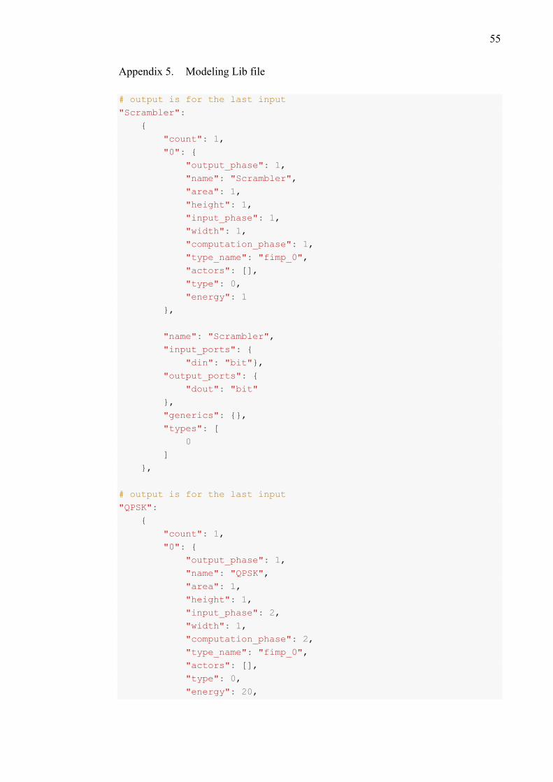
55
Appendix 5. Modeling Lib file
# output is for the last input
"Scrambler":
{
"count": 1,
"0": {
"output_phase": 1,
"name": "Scrambler",
"area": 1,
"height": 1,
"input_phase": 1,
"width": 1,
"computation_phase": 1,
"type_name": "fimp_0",
"actors": [],
"type": 0,
"energy": 1
},
"name": "Scrambler",
"input_ports": {
"din": "bit"},
"output_ports": {
"dout": "bit"
},
"generics": {},
"types": [
0
]
},
# output is for the last input
"QPSK":
{
"count": 1,
"0": {
"output_phase": 1,
"name": "QPSK",
"area": 1,
"height": 1,
"input_phase": 2,
"width": 1,
"computation_phase": 2,
"type_name": "fimp_0",
"actors": [],
"type": 0,
"energy": 20,

56
},
"name": "QPSK",
"input_ports": {
"din": "bit"},
"output_ports": {
"dout": "complex"
},
"generics": {},
"types": [
0
]
},
# output is for the last input
"QAM_16":
{
"count": 1,
"0": {
"output_phase": 1,
"name": "QAM_16",
"area": 1,
"height": 1,
"input_phase": 4,
"width": 1,
"computation_phase": 4,
"type_name": "fimp_0",
"actors": [],
"type": 0,
"energy": 30,
},
"name": "QAM_16",
"input_ports": {
"din": "bit"},
"output_ports": {
"dout": "complex"
},
"generics": {},
"types": [
0
]
},
# output is for the last input
"QAM_64":
{
"count": 1,

57
"0": {
"output_phase": 1,
"name": "QAM_64",
"area": 1,
"height": 1,
"input_phase": 6,
"width": 1,
"computation_phase": 6,
"type_name": "fimp_0",
"actors": [],
"type": 0,
"energy": 50,
},
"name": "QAM_64",
"input_ports": {
"din": "bit"},
"output_ports": {
"dout": "complex"
},
"generics": {},
"types": [
0
]
},
# input: 2 streams
# each stream is 600 complex symbols
# output: 300 X 4 matrix complex symbols
"LayerMapper_600_300":
{
"count": 1,
"0": {
"output_phase": 300,
"name": "LayerMapper_600_300",
"area": 1,
"height": 1,
"input_phase": 600,
"width": 1,
"computation_phase": 900,
"type_name": "fimp_0",
"actors": [],
"type": 0,
"energy": 128
},
"name": "LayerMapper_600_300",
"input_ports": {

58
"din1": "complex",
"din2": "complex"
},
"output_ports": {
"dout1": "complex",
"dout2": "complex",
"dout3": "complex",
"dout4": "complex"
},
"generics": {},
"types": [
0
]
},
# input: 2 streams
# each stream is 600 complex symbols
# output: 300 X 4 matrix complex symbols
"LayerMapper_1200_600":
{
"count": 1,
"0": {
"output_phase": 600,
"name": "LayerMapper_1200_600",
"area": 1,
"height": 1,
"input_phase": 1200,
"width": 1,
"computation_phase": 1800,
"type_name": "fimp_0",
"actors": [],
"type": 0,
"energy": 256
},
"name": "LayerMapper_1200_600",
"input_ports": {
"din1": "complex",
"din2": "complex"
},
"output_ports": {
"dout1": "complex",
"dout2": "complex",
"dout3": "complex",
"dout4": "complex"
},
"generics": {},
"types": [

59
0
]
},
# input: 2 streams
# each stream is 600 complex symbols
# output: 300 X 4 matrix complex symbols
"LayerMapper_2400_1200":
{
"count": 1,
"0": {
"output_phase": 1200,
"name": "LayerMapper_2400_1200",
"area": 1,
"height": 1,
"input_phase": 2400,
"width": 1,
"computation_phase": 3600,
"type_name": "fimp_0",
"actors": [],
"type": 0,
"energy": 512
},
"name": "LayerMapper_2400_1200",
"input_ports": {
"din1": "complex",
"din2": "complex"
},
"output_ports": {
"dout1": "complex",
"dout2": "complex",
"dout3": "complex",
"dout4": "complex"
},
"generics": {},
"types": [
0
]
},
# 1 symbol to 1 symbol
# it has internal states
"Precoding":
{
"count": 5,
"0": {
"output_phase": 1,

60
"name": "Precoding",
"area": 1,
"height": 1,
"input_phase": 1,
"width": 1,
"computation_phase": 164,
"type_name": "fimp_0",
"actors": [],
"type": 0,
"energy": 9088
},
"1": {
"output_phase": 1,
"name": "Precoding",
"area": 2,
"height": 2,
"input_phase": 1,
"width": 1,
"computation_phase": 84,
"type_name": "fimp_1",
"actors": [],
"type": 1,
"energy": 9200
},
"2": {
"output_phase": 1,
"name": "Precoding",
"area": 4,
"height": 2,
"input_phase": 1,
"width": 2,
"computation_phase": 44,
"type_name": "fimp_2",
"actors": [],
"type": 0,
"energy": 9500
},
"3": {
"output_phase": 1,
"name": "Precoding",
"area": 8,
"height": 4,
"input_phase": 1,
"width": 2,
"computation_phase": 32,

61
"type_name": "fimp_3",
"actors": [],
"type": 0,
"energy": 9700
},
"4": {
"output_phase": 1,
"name": "Precoding",
"area": 16,
"height": 4,
"input_phase": 1,
"width": 4,
"computation_phase": 24,
"type_name": "fimp_3",
"actors": [],
"type": 0,
"energy": 9900
},
"name": "Precoding",
"input_ports": {
"din1": "complex",
"din2": "complex",
"din3": "complex",
"din4": "complex",
},
"output_ports": {
"dout1": "complex",
"dout2": "complex",
"dout3": "complex",
"dout4": "complex",
},
"generics": {},
"types": [
0,
1,
2,
3,
4
]
},
# PDSCH
"Remapper_300_512":
{
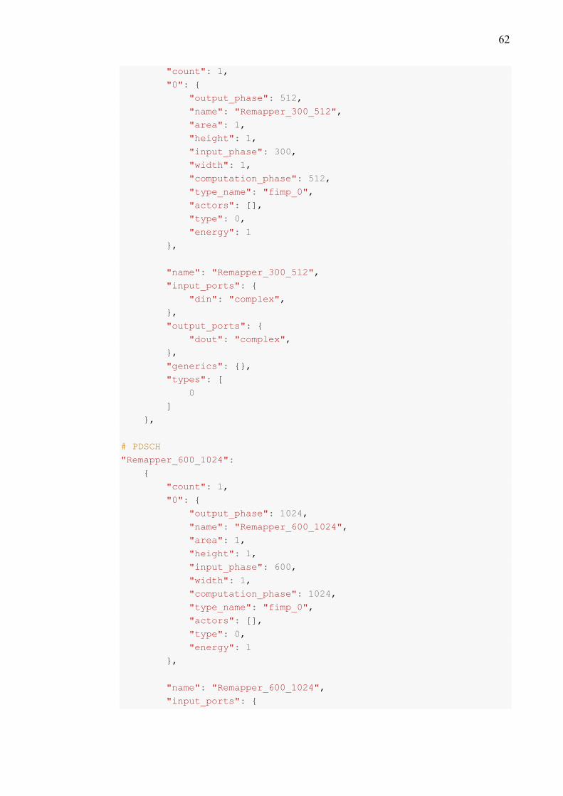
62
"count": 1,
"0": {
"output_phase": 512,
"name": "Remapper_300_512",
"area": 1,
"height": 1,
"input_phase": 300,
"width": 1,
"computation_phase": 512,
"type_name": "fimp_0",
"actors": [],
"type": 0,
"energy": 1
},
"name": "Remapper_300_512",
"input_ports": {
"din": "complex",
},
"output_ports": {
"dout": "complex",
},
"generics": {},
"types": [
0
]
},
# PDSCH
"Remapper_600_1024":
{
"count": 1,
"0": {
"output_phase": 1024,
"name": "Remapper_600_1024",
"area": 1,
"height": 1,
"input_phase": 600,
"width": 1,
"computation_phase": 1024,
"type_name": "fimp_0",
"actors": [],
"type": 0,
"energy": 1
},
"name": "Remapper_600_1024",
"input_ports": {
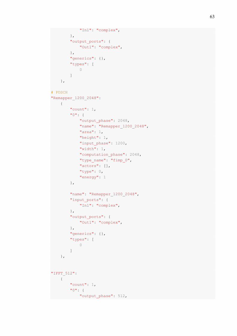
63
"In1": "complex",
},
"output_ports": {
"Out1": "complex",
},
"generics": {},
"types": [
0
]
},
# PDSCH
"Remapper_1200_2048":
{
"count": 1,
"0": {
"output_phase": 2048,
"name": "Remapper_1200_2048",
"area": 1,
"height": 1,
"input_phase": 1200,
"width": 1,
"computation_phase": 2048,
"type_name": "fimp_0",
"actors": [],
"type": 0,
"energy": 1
},
"name": "Remapper_1200_2048",
"input_ports": {
"In1": "complex",
},
"output_ports": {
"Out1": "complex",
},
"generics": {},
"types": [
0
]
},
"IFFT_512":
{
"count": 1,
"0": {
"output_phase": 512,

64
"name": "IFFT_512",
"area": 1,
"height": 1,
"input_phase": 512,
"width": 1,
"computation_phase": 2304,
"type_name": "fimp_0",
"actors": [],
"type": 0,
"energy": 881100
},
"1": {
"output_phase": 512,
"name": "IFFT_512",
"area": 2,
"height": 1,
"input_phase": 512,
"width": 2,
"computation_phase": 1152,
"type_name": "fimp_1",
"actors": [],
"type": 1,
"energy": 883055
},
"2": {
"output_phase": 512,
"name": "IFFT_512",
"area": 4,
"height": 2,
"input_phase": 512,
"width": 2,
"computation_phase": 576,
"type_name": "fimp_2",
"actors": [],
"type": 2,
"energy": 916666
},
"name": "IFFT_512",
"input_ports": {
"din": "complex"
},
"output_ports": {
"dout": "complex"
},
65
"generics": {},
"types": [
0,
1,
2
]
},
"IFFT_1024":
{
"count": 1,
"0": {
"output_phase": 1024,
"name": "IFFT_1024",
"area": 1,
"height": 1,
"input_phase": 1024,
"width": 1,
"computation_phase": 5120,
"type_name": "fimp_0",
"actors": [],
"type": 0,
"energy": 1958000
},
"1": {
"output_phase": 1024,
"name": "IFFT_1024",
"area": 2,
"height": 1,
"input_phase": 1024,
"width": 2,
"computation_phase": 2560,
"type_name": "fimp_1",
"actors": [],
"type": 1,
"energy": 1962344
},
"2": {
"output_phase": 1024,
"name": "IFFT_1024",
"area": 4,
"height": 2,
"input_phase": 1024,
"width": 2,
66
"computation_phase": 1280,
"type_name": "fimp_2",
"actors": [],
"type": 2,
"energy": 2037035
},
"name": "IFFT_1024",
"input_ports": {
"din": "complex"
},
"output_ports": {
"dout": "complex"
},
"generics": {},
"types": [
0,
1,
2
]
},
"IFFT_2048":
{
"count": 3,
"0": {
"output_phase": 2048,
"name": "IFFT_2048",
"area": 1,
"height": 1,
"input_phase": 2048,
"width": 1,
"computation_phase": 11264,
"type_name": "fimp_0",
"actors": [],
"type": 0,
"energy": 2883600
},
"1": {
"output_phase": 2048,
"name": "IFFT_2048",
"area": 1,
"height": 1,
"input_phase": 2048,
"width": 2,
"computation_phase": 5632,

67
"type_name": "fimp_1",
"actors": [],
"type": 1,
"energy": 2890000
},
"2": {
"output_phase": 2048,
"name": "IFFT_2048",
"area": 1,
"height": 2,
"input_phase": 2048,
"width": 2,
"computation_phase": 2816,
"type_name": "fimp_2",
"actors": [],
"type": 2,
"energy": 3000000
},
"name": "IFFT_2048",
"input_ports": {
"din": "complex"
},
"output_ports": {
"dout": "complex"
},
"generics": {},
"types": [
0,
1,
2
]
}