MA1595/MA1596/MA159 Peak-Current-Mode Controllers … · MA1595/MA1596/MA159 Peak-Current-Mode...
22
MAX17595/MAX17596/MAX17597 Peak-Current-Mode Controllers for Flyback and Boost Regulators General Description The MAX17595–MAX17597 is a family of peak-current- mode controllers for design of wide input-voltage flyback and boost regulators. The MAX17595 offers optimized input thresholds for universal input AC-DC converters and telecom DC-DC (36V to 72V input range) power supplies. The MAX17596/MAX17597 offer input thresholds suitable for low-voltage DC-DC applications (4.5V to 36V). The MAX17597 implements a boost converter. All three controllers contain a built-in gate driver for external n-channel MOSFETs. The MAX17595–MAX17597 house an internal error amplifier with 1% accurate reference, eliminating the need for an external reference. The switching frequency is programma- ble from 100kHz to 1MHz with an accuracy of 8%, allow- ing optimization of magnetic and filter components, resulting in compact and cost-effective power conversion. For EMI-sensitive applications, the MAX17595–MAX17597 family incorporates a programmable frequency dithering scheme, enabling low-EMI spread-spectrum operation. Users can start the power supply precisely at the desired input voltage, implement input overvoltage protection, and program soft-start time. A programmable slope compensation scheme is provided to ensuree stability of the peak- current-mode control scheme. Hiccup-mode overcurrent protection and thermal shutdown are provided to minimize dissipation in overcurrent and overtemperature fault conditions. Applications ● Universal Input Offline AC-DC Power Supplies ● Wide-Range DC-Input Flyback/Boost Battery Chargers ● Battery-Powered Applications ● Industrial and Telecom Applications Benefits and Features ● Programmable Switching Frequency Allows Optimization of the Magnetic and Filter Components, Resulting in Compact, Cost-Effective, Efficient Isolated/Non-Isolated Power Supplies • 100kHz to 1MHz Programmable Switching Frequency with Optional Synchronization • Peak Current Mode Control Provides Excellent Transient Response - Offline (Universal Input AC) and Telecom (36V to 72V) Flyback Controller—MAX17595 - DC-DC (4.5V to 36V) Flyback Controller— MAX17596 - Nonsynchronous (4.5V to 36V) Boost PWM Controller—MAX17597 • 3mm x 3mm TQFN Package ● Programmable Frequency Dithering Enables Low- EMI Spread-Spectrum Operation ● Integrated Protection Features Enhance System Reliability • Adjustable Current Limit with External Current- Sense Resistor • Fast Cycle-By-Cycle Peak Current Limiting • Hiccup-Mode Short-Circuit Protection • Overtemperature Protection • Programmable Soft-Start and Slope Compensation • Input Overvoltage Protection 19-6178; Rev 4; 5/15 Ordering Information/Selector Guide appears at end of data sheet. EVALUATION KIT AVAILABLE For pricing, delivery, and ordering information, please contact Maxim Direct at 1-888-629-4642, or visit Maxim’s website at www.maximintegrated.com.
Transcript of MA1595/MA1596/MA159 Peak-Current-Mode Controllers … · MA1595/MA1596/MA159 Peak-Current-Mode...
MAX17595/MAX17596/MAX17597
Peak-Current-Mode Controllers for Flyback and Boost Regulators
General Description
The MAX17595–MAX17597 is a family of peak-current-mode controllers for design of wide input-voltage flyback and boost regulators. The MAX17595 offers optimized input thresholds for universal input AC-DC converters and telecom DC-DC (36V to 72V input range) power supplies. The MAX17596/MAX17597 offer input thresholds suitable for low-voltage DC-DC applications (4.5V to 36V). The MAX17597 implements a boost converter. All three controllers contain a built-in gate driver for external n-channel MOSFETs.
The MAX17595–MAX17597 house an internal error amplifier with 1% accurate reference, eliminating the need for an external reference. The switching frequency is programma-ble from 100kHz to 1MHz with an accuracy of 8%, allow-ing optimization of magnetic and filter components, resulting in compact and cost-effective power conversion. For EMI-sensitive applications, the MAX17595–MAX17597 family incorporates a programmable frequency dithering scheme, enabling low-EMI spread-spectrum operation.
Users can start the power supply precisely at the desired input voltage, implement input overvoltage protection, and program soft-start time. A programmable slope compensation scheme is provided to ensuree stability of the peak-current-mode control scheme.
Hiccup-mode overcurrent protection and thermal shutdown are provided to minimize dissipation in overcurrent and overtemperature fault conditions.
Applications
● Universal Input Offline AC-DC Power Supplies ● Wide-Range DC-Input Flyback/Boost Battery
Chargers ● Battery-Powered Applications ● Industrial and Telecom Applications
Benefits and Features
● Programmable Switching Frequency Allows Optimization of the Magnetic and Filter Components, Resulting in Compact, Cost-Effective, Efficient Isolated/Non-Isolated Power Supplies• 100kHz to 1MHz Programmable Switching
Frequency with Optional Synchronization• Peak Current Mode Control Provides Excellent
Transient Response - Offline (Universal Input AC) and Telecom (36V to 72V)
Flyback Controller—MAX17595 - DC-DC (4.5V to 36V) Flyback Controller—MAX17596
- Nonsynchronous (4.5V to 36V) Boost PWM Controller—MAX17597
• 3mm x 3mm TQFN Package ● Programmable Frequency Dithering Enables Low-
EMI Spread-Spectrum Operation ● Integrated Protection Features Enhance System
Reliability• Adjustable Current Limit with External Current-
Sense Resistor• Fast Cycle-By-Cycle Peak Current Limiting• Hiccup-Mode Short-Circuit Protection• Overtemperature Protection• Programmable Soft-Start and Slope Compensation• Input Overvoltage Protection
19-6178; Rev 4; 5/15
Ordering Information/Selector Guide appears at end of data sheet.
EVALUATION KIT AVAILABLE
For pricing, delivery, and ordering information, please contact Maxim Direct at 1-888-629-4642, or visit Maxim’s website at www.maximintegrated.com.

MAX17595/MAX17596/MAX17597
Peak-Current-Mode Controllers for Flyback and Boost Regulators
2Maxim Integrated
VIN to SGND ..........................................................-0.3V to +40VVDRV to SGND ..................................-0.3V to +16V (MAX17595)VDRV to SGND ..........-0.3V to +6V (MAX17596 and MAX17597)NDRV to SGND .................................... -0.3V to +(VDRV + 0.3)VEN/UVLO to SGND .................................. -0.3V to +(VIN + 0.3)VOVI, RT, DITHER, COMP, SS, FB,
SLOPE to SGND .................................................... -0.3V to +6VCS to SGND ............................................................-0.8V to +6VPGND to SGND ....................................................-0.3V to +0.3V
Maximum Input/Output Current (Continuous)VIN, VDRV..........................................................................100mANDRV (pulsed, for less than 100ns) .......................... 1.5A/-0.9AContinuous Power Dissipation TQFN (single-layer board) (derate 20.8mW/NC above +70NC) ............................1666mWOperating Temperature Range ........................ -40NC to +125NCStorage Temperature Range ............................ -65NC to +150NCJunction Temperature .....................................................+150NCLead Temperature (soldering, 10s) ................................+300NCSoldering Temperature (reflow) ......................................+260NC
ABSOLUTE MAXIMUM RATINGS
Note 1: Package thermal resistances were obtained using the method described in JEDEC specification JESD51-7, using a four-layer board. For detailed information on package thermal considerations, refer to www.maximintegrated.com/thermal-tutorial.
Stresses beyond those listed under “Absolute Maximum Ratings” may cause permanent damage to the device. These are stress ratings only, and functional opera-tion of the device at these or any other conditions beyond those indicated in the operational sections of the specifications is not implied. Exposure to absolute maximum rating conditions for extended periods may affect device reliability.
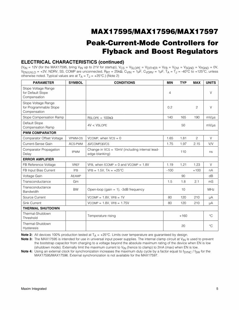
ELECTRICAL CHARACTERISTICS(VIN = 12V (for the MAX17595, bring VIN up to 21V for startup), VCS = VSLOPE = VDITHER = VFB = VOVI = VSGND = VPGND = 0V, VEN/UVLO = +2V; NDRV, SS, COMP are unconnected, RRT = 25kI, CVIN = 1FF, CVDRV = 1FF, TA = TJ = -40NC to +125NC, unless otherwise noted. Typical values are at TA = TJ = +25NC.) (Note 2)
Junction-to-Ambient Thermal Resistance (qJA) ..............48°C/W Junction-to-Case Thermal Resistance (qJC) .....................7°C/W
PACKAGE THERMAL CHARACTERISTICS (Note 1)
PARAMETER SYMBOL CONDITIONS MIN TYP MAX UNITS
INPUT SUPPLY (VIN)
VIN Voltage Range VINMAX17595 8 29
VMAX17596/MAX17597 4.5 36
VIN Bootstrap UVLO Wakeup
VIN-UVR VIN rising #MAX17595 18.5 20 21.5
VMAX17596/MAX17597 3.8 4.1 4.4
VIN Bootstrap UVLO Shutdown Level
VIN-UVF VIN falling $MAX17595 6.5 7 7.5
VMAX17596/MAX17597 3.6 3.9 4.2
VIN Supply Startup Current (Under UVLO)
IVIN-STARTUP
VIN < UVLO 20 32 FA
VIN Supply Shutdown Current
IIN-SH VEN = 0V 20 32 FA
VIN Supply Current IIN-SW Switching, fSW = 400kHz 2 mA
VIN Clamp Voltage VINCMAX17595, IVIN = 2mA sinking, VEN = 0V (Note 3)
30 33 36 V
ENABLE (EN)
EN Undervoltage Threshold
VENR VEN rising # 1.16 1.21 1.26V
VENF VEN falling $ 1.1 1.15 1.2
EN Input Leakage Current IEN VEN = 1.5V, TA = +25NC -100 +100 nA

MAX17595/MAX17596/MAX17597
Peak-Current-Mode Controllers for Flyback and Boost Regulators
3Maxim Integrated
ELECTRICAL CHARACTERISTICS (continued)(VIN = 12V (for the MAX17595, bring VIN up to 21V for startup), VCS = VSLOPE = VDITHER = VFB = VOVI = VSGND = VPGND = 0V, VEN/UVLO = +2V; NDRV, SS, COMP are unconnected, RRT = 25kI, CVIN = 1FF, CVDRV = 1FF, TA = TJ = -40NC to +125NC, unless otherwise noted. Typical values are at TA = TJ = +25NC.) (Note 2)
PARAMETER SYMBOL CONDITIONS MIN TYP MAX UNITS
INTERNAL LDO (VDRV)
VDRV Output Voltage Range
VDRV
8V < VIN < 15V and 0mA < IVDRV < 50mA (MAX17595)
7.1 7.4 7.7
V6V < VIN < 15V and 0mA < IVDRV < 50mA (MAX17596/MAX17597)
4.7 4.9 5.1
VDRV Current Limit IVDRV-MAX 70 100 mA
VDRV Dropout VVDRV-DOVIN = 4.5V, IVDRV = 20mA (MAX17596/MAX17597)
4.2
V
OVERVOLTAGE PROTECTION (OVI)
OVI Overvoltage ThresholdVOVIR VOVI rising # 1.16 1.21 1.26
VVOVIF VOVI falling $ 1.1 1.15 1.2
OVI Masking Delay tOVI-MD 2 Fs
OVI Input Leakage Current IOVI VOVI = 1V, TA = +25NC -100 +100 nA
OSCILLATOR (RT)
NDRV Switching Frequency Range
fSW 100 1000 kHz
NDRV Switching Frequency Accuracy
-8 +8 %
Maximum Duty Cycle DMAX fSW = 400kHz(MAX17595/MAX17596) 46 48 50
%(MAX17597) 90 92.5 95
SYNCHRONIZATION (DITHER/SYNC)
Synchronization Logic-High Input
VHI-SYNC 3 V
Synchronization Pulse Width
50 ns
Synchronization Frequency Range
fSYNC (MAX17595/MAX17596) (Note 4) 1.1 x fSW 1.8 x fSW Hz
DITHERING RAMP GENERATOR (DITHER/SYNC)
Charging Current 45 50 55 FA
Discharging Current 43 50 57 FA
Ramp-High Trip Point 2 V
Ramp-Low Trip Point 0.4 V
MAX17595/MAX17596/MAX17597
Peak-Current-Mode Controllers for Flyback and Boost Regulators
4Maxim Integrated
ELECTRICAL CHARACTERISTICS (continued)(VIN = 12V (for the MAX17595, bring VIN up to 21V for startup), VCS = VSLOPE = VDITHER = VFB = VOVI = VSGND = VPGND = 0V, VEN/UVLO = +2V; NDRV, SS, COMP are unconnected, RRT = 25kI, CVIN = 1FF, CVDRV = 1FF, TA = TJ = -40NC to +125NC, unless otherwise noted. Typical values are at TA = TJ = +25NC.) (Note 2)
PARAMETER SYMBOL CONDITIONS MIN TYP MAX UNITS
SOFT-START (SS)
Soft-Start Charging Current ISSCH 9 10 11 FA
SS Bias Voltage VSS 1.19 1.21 1.23 V
NDRV DRIVER (NDRV)
Pulldown Impedance RNDRV-N INDRV (sinking) = 100mA 1.37 3 I
Pullup Impedance RNDRV-P INDRV (sourcing) = 50mA 4.26 8.5 I
Peak Sink Current CNDRV = 10nF 1.5 A
Peak Source Current CNDRV = 10nF 0.9 A
Fall Time tNDRV-F CNDRV = 1nF 10 ns
Rise Time tNDRV-R CNDRV = 1nF 20 ns
CURRENT-LIMIT COMPARATOR (CS)
Cycle-by-Cycle Peak Current-Limit Threshold
VCS-PEAK 290 305 320 mV
Cycle-by-Cycle Runaway Current-Limit Threshold
VCS-RUN 340 360 380 mV
Current-Sense Leading-Edge Blanking Time
tCS-BLANK From NDRV rising # edge 70 ns
Propagation Delay from Comparator Input to NDRV
tPDCSFrom CS rising (10mV overdrive) to NDRV falling (excluding leading edge blanking)
40 ns
Number of Consecutive Peak- Current-Limit Events to Hiccup
NHICCUP-P 8 events
Number of Runaway-Current-Limit Events to Hiccup
NHICCUP-R 1 event
Overcurrent Hiccup Timeout
32,768 cycle
Minimum On-Time tON-MIN 90 130 170 ns
SLOPE COMPENSATION (SLOPE)
Slope Bias Current ISLOPE 9 10 11 FA
Slope Resistor Range 25 200 kI
MAX17595/MAX17596/MAX17597
Peak-Current-Mode Controllers for Flyback and Boost Regulators
5Maxim Integrated
ELECTRICAL CHARACTERISTICS (continued)(VIN = 12V (for the MAX17595, bring VIN up to 21V for startup), VCS = VSLOPE = VDITHER = VFB = VOVI = VSGND = VPGND = 0V, VEN/UVLO = +2V; NDRV, SS, COMP are unconnected, RRT = 25kI, CVIN = 1FF, CVDRV = 1FF, TA = TJ = -40NC to +125NC, unless otherwise noted. Typical values are at TA = TJ = +25NC.) (Note 2)
Note 2: All devices 100% production tested at TA = +25°C. Limits over temperature are guaranteed by design.Note 3: The MAX17595 is intended for use in universal input power supplies. The internal clamp circuit at VIN is used to prevent
the bootstrap capacitor from charging to a voltage beyond the absolute maximum rating of the device when EN is low (shutdown mode). Externally limit the maximum current to VIN (hence to clamp) to 2mA (max) when EN is low.
Note 4: Using an external clock for synchronization increases the maximum duty cycle by a factor equal to fSYNC / fSW for the MAX17595/MAX17596. External synchronization is not available for the MAX17597.
PARAMETER SYMBOL CONDITIONS MIN TYP MAX UNITS
Slope Voltage Range for Default Slope Compensation
4 V
Slope Voltage Range for Programmable Slope Compensation
0.2 2 V
Slope Compensation Ramp RSLOPE = 100kW 140 165 190 mV/Fs
Default Slope Compensation Ramp
4V < VSLOPE 50 mV/Fs
PWM COMPARATOR
Comparator Offset Voltage VPWM-OS VCOMP, when VCS = 0 1.65 1.81 2 V
Current-Sense Gain ACS-PWM DVCOMP/DVCS 1.75 1.97 2.15 V/V
Comparator Propagation Delay
tPWMChange in VCS = 10mV (including internal lead-edge blanking)
110 ns
ERROR AMPLIFIER
FB Reference Voltage VREF VFB, when ICOMP = 0 and VCOMP = 1.8V 1.19 1.21 1.23 V
FB Input Bias Current IFB VFB = 1.5V, TA = +25NC -100 +100 nA
Voltage Gain AEAMP 90 dB
Transconductance Gm 1.5 1.8 2.1 mS
Transconductance Bandwidth
BW Open-loop (gain = 1), -3dB frequency 10 MHz
Source Current VCOMP = 1.8V, VFB = 1V 80 120 210 FA
Sink Current VCOMP = 1.8V, VFB = 1.75V 80 120 210 FA
THERMAL SHUTDOWN
Thermal-Shutdown Threshold
Temperature rising +160 NC
Thermal-Shutdown Hysteresis
20 NC

MAX17595/MAX17596/MAX17597
Peak-Current-Mode Controllers for Flyback and Boost Regulators
6Maxim Integrated
Typical Operating Characteristics(VIN = 15V, VEN/UVLO = +2V, COMP = open, CVIN = 1FF, CVDRV = 1FF, TA = TJ = -40NC to +125NC, unless otherwise noted.)
BOOTSTRAP UVLO WAKE-UP LEVELvs. TEMPERATURE (MAX17595)
MAX17595/6/7 toc01
TEMPERATURE (°C)
BOOT
STRA
P UV
LO W
AKE-
UP L
EVEL
(V)
20 40 60 80 100 1200-20
19.99
20.00
20.01
20.02
20.03
20.04
19.98-40
VIN FALLING THRESHOLD vs. TEMPERATURE(MAX17596/MAX17597)
MAX17595/6/7 toc04
TEMPERATURE (°C)
V IN
UVLO
SHU
TDOW
N TH
RESH
OLD
(V)
20 40 60 80 100 1200-20
3.92
3.97-40
3.88
3.89
3.90
3.91
EN/UVLO FALLING THRESHOLDvs. TEMPERATURE
MAX17595/6/7 toc06
TEMPERATURE (°C)
EN/U
VLO
FALL
ING
THRE
SHOL
D (V
)
20 40 60 80 100 1200-20
1.149
1.145-40
1.146
1.147
1.148
EN/UVLO RISING THRESHOLDvs. TEMPERATURE
MAX17595/6/7 toc05
TEMPERATURE (°C)
EN/U
VLO
RISI
NG T
HRES
HOLD
(V)
20 40 60 80 100 1200-20
1.209
1.202-40
1.203
1.204
1.205
1.206
1.207
1.208
OVI RISING THRESHOLDvs. TEMPERATURE
MAX17595/6/7 toc07
TEMPERATURE (°C)
OVI R
ISIN
G TH
RESH
OLD
(V)
20 40 60 80 100 1200-20
1.211
1.207-40
1.208
1.209
1.210
VIN WAKE-UP LEVEL vs. TEMPERATURE(MAX17596/MAX17597)
MAX17595/6/7 toc02
TEMPERATURE (°C)
V IN
WAK
E-UP
LEV
EL (V
)
20 40 60 80 100 1200-20
4.13
4.07-40
4.08
4.09
4.11
4.10
4.12
VIN FALLING THRESHOLDvs. TEMPERATURE (MAX17595)
MAX17595/6/7 toc03
TEMPERATURE (°C)
V IN
BOOT
STRA
P UV
LO S
HUTD
OWN
LEVE
L (V
)
20 40 60 80 100 1200-20
7.000
7.005
7.010
7.015
7.020
7.025
6.995-40

MAX17595/MAX17596/MAX17597
Peak-Current-Mode Controllers for Flyback and Boost Regulators
7Maxim Integrated
Typical Operating Characteristics (continued)(VIN = 15V, VEN/UVLO = +2V, COMP = open, CVIN = 1FF, CVDRV = 1FF, TA = TJ = -40NC to +125NC, unless otherwise noted.)
OVI FALLING THRESHOLDvs. TEMPERATURE
MAX17595/6/7 toc08
TEMPERATURE (°C)
OVI F
ALLI
NG T
HRES
HOLD
(V)
20 40 60 80 100 1200-20
1.1480
1.1485
1.1490
1.1495
1.1500
1.1505
1.1475-40
NDRV SWITCHING FREQUENCYvs. RESISTOR
MAX17595/6/7 toc11
FREQUENCY SELECTION RESISTOR (kI)
NDRV
SW
ITCH
ING
FREQ
UENC
Y (k
Hz)
1000
05 15 25 35 45 55 65 75 85 95
100
200
300
400
600
700
800
900
500
FREQUENCY DITHERING vs. RDITHER
RDITHER (kI)
FREQ
UENC
Y D
ITHE
RING
(%)
900800700600500400300
4
6
8
10
12
14
2200 1000
MAX17595/6/7 toc13
NDRV SWITCHING FREQUENCY vs. TEMPERATURE
MAX17595/6/7 toc12
TEMPERATURE (°C)
NDRV
SW
ITCH
ING
FREQ
UENC
Y (k
Hz)
20 40 60 80 100 1200-20
950
850
750
650
550
450
350
250
150
50-40
RRT = 10kI
RRT = 100kI
SWITCHING WAVEFORMS (MAX17595)MAX17595/6/7 toc14
IPRI1A/div
4µs/div
VDRAIN100V/div
VIN SUPPLY CURRENT UNDER UVLOvs. TEMPERATURE
MAX17595/6/7 toc09
TEMPERATURE (°C)
V IN
SUPP
LY C
URRE
NT U
NDER
UVL
O (µ
A)
20 40 60 80 100 1200-20
20.5
21.5
22.5
23.5
24.5
25.5
19.5-40
SWITCHING CURRENTvs. TEMPERATURE
MAX17595/6/7 toc10
TEMPERATURE (°C)
SWIT
CHIN
G CU
RREN
T (m
A)
20 40 60 80 100 1200-20
2.5
1.5-40
1.6
1.7
1.8
1.9
2.1
2.2
2.3
2.4
2.0

MAX17595/MAX17596/MAX17597
Peak-Current-Mode Controllers for Flyback and Boost Regulators
8Maxim Integrated
Typical Operating Characteristics (continued)(VIN = 15V, VEN/UVLO = +2V, COMP = open, CVIN = 1FF, CVDRV = 1FF, TA = TJ = -40NC to +125NC, unless otherwise noted.)
ENABLE STARTUPMAX17595/6/7 toc15
COMP1V/div
2ms/div
VOUT10V/div
EN/UVLO5V/div
SWITCHING CURRENTvs. SWITCHING FREQUENCY
SWITCHING FREQUENCY (Hz)
SWIT
CHIN
G CU
RREN
T (m
A)
900800700500 600400300200
1.7
1.9
2.1
2.3
2.5
1.5100 1000
MAX17595/6/7 toc18
BODE PLOT (FIGURE 9 OUTPUT)MAX17595/6/7 toc20
PHASE36°/div
GAIN10dB/divBANDWIDTH = 11.5kHz
PHASE MARGIN = 50.9°
6 68 2 24 41 8 1
LOAD TRANSIENT RESPONSE(FIGURE 9 OUTPUT)
MAX17595/6/7 toc19
0.4ms/div
VOUT (AC)0.5V/div
ILOAD0.5A/div
LOAD CURRENT (A)
0 1.41.21.00.80.60.40.2
EFFICIENCY GRAPH (FIGURE 9 OUTPUT)
EFFI
CIEN
CY (%
)
10
20
30
40
60
70
80
90
100
0
50
MAX17595/6/7 toc21
VDC = 120V
ENABLE SHUTDOWNMAX17595/6/7 toc16
COMP1V/div
400µs/div
VOUT10V/div
EN/UVLO5V/div
HICCUP OPERATIONMAX17595/6/7 toc17
1ms/div
VOUT10V/div
VDRAIN100V/div
IPRI2A/div

MAX17595/MAX17596/MAX17597
Peak-Current-Mode Controllers for Flyback and Boost Regulators
9Maxim Integrated
Pin Description
Pin Configuration
PIN NAME FUNCTION
1, 12 N.C. No Connection
2 SLOPE
Slope Compensation Input. A resistor, RSLOPE, connected from SLOPE to SGND programs the amount of slope compensation with reference-voltage soft-start mode. Connecting this pin to SGND enables duty-cycle soft-start with default slope compensation of 50mV/Fs. Setting VSLOPE > 4V enables reference voltage soft-start with default slope compensation of 50mV/Fs.
3 RTSwitching Frequency Programming Resistor Connection. Connect resistor RRT from RT to SGND to set the PWM switching frequency.
4 DITHER/SYNC
Frequency Dithering Programming or Synchronization Connection. For spread-spectrum frequency operation, connect a capacitor from DITHER to SGND, and a resistor from DITHER to RT. To synchronize the internal oscillator to the externally applied frequency (MAX17595/MAX17596 only), connect DITHER/SYNC to the synchronization pulse.
5 COMPTransconductance Amplifier Output. Connect the frequency compensation network between COMP and SGND.
6 FB Transconductance Amplifier Inverting Input
7 SSSoft-Start Capacitor Pin for Flyback Regulator. Connect a capacitor CSS from SS to SGND to set the soft-start time interval.
8 SGND Signal Ground. Connect SGND to the signal ground plane.
9 CS Current-Sense Input. Peak-current-limit trip voltage is 300mV (typ).
10 PGND Power Ground. Connect PGND to the power ground plane.
11 NDRV External Switching nMOS Gate-Driver Output
15
16
14
13
5
6
7
RT
DITH
ER/
SYNC
8
N.C.
PGND
CSN.C.
1 3
VIN
4
12 10 9
EN/ UVLO
OVI EP
SGND
SS
FB
COMP
SLOP
END
RV
2
11
VDRV
TQFN
MAX17595MAX17596
TOP VIEW
+
15
16
14
13
5
6
7
RT
DITH
ER
8
N.C.
PGND
CSN.C.
1 3
VIN
4
12 10 9
EN/ UVLO
OVI EP
SGND
SS
FB
COMP
SLOP
END
RV
2
11
VDRV
TQFN
MAX17597
+
MAX17595/MAX17596/MAX17597
Peak-Current-Mode Controllers for Flyback and Boost Regulators
10Maxim Integrated
Pin Description (continued)
Detailed Description
The MAX17595 offers a bootstrap UVLO wake-up level of 20V with a wide hysteresis, and is optimized for imple-menting isolated and nonisolated universal (85V to 265V AC) offline single-switch flyback converter or telecom (36V to 72V) power supplies. The MAX17596/MAX17597 offer a UVLO wake-up level of 4.4V and are well-suited for low-voltage DC-DC flyback/boost power supplies. An internal 1% reference (1.21V) can be used to regulate the output in nonisolated flyback and boost applications. Additional semiregulated outputs, if needed, can be gen-erated by using additional secondary windings on the flyback converter transformer.
The MAX17595/MAX17596/MAX17597 family utilizes peak-current-mode control and external compensation for optimizing closed-loop performance. The devices include cycle-by-cycle peak current limit, and eight consecutive occurrences of current-limit-event trigger hiccup mode, which protects external components by halting switching for a period of 32,768 cycles. .
Input Voltage Range (VIN)The MAX17595 has no limitation on maxi-mum input voltage, as long as the external components are rated suitably and the maximum operating voltages of the MAX17595 are respected.
The MAX17595 implements a rising and falling UVLO threshold that allows it to be successfully used in univer-sal input (85V to 265V AC) rectified bus applications, in rectified 3-phase DC bus applications, and in telecom (36V to 72V DC) applications.
The MAX17596/MAX17597 are intended to implement flyback (isolated and nonisolated) and boost convert-ers. The VIN pin of the MAX17596/MAX17597 has a maximum operating voltage of 36V. The MAX17596/MAX17597 implement rising and falling thresholds on the VIN pin that assume power-supply startup schemes typical of low-voltage DC-DC applications, down to an input voltage of 4.5V DC. Therefore, flyback /boost converters with a 4.5V to 36V supply voltage range can be implemented with the MAX17596/MAX17597.
Internal Linear Regulator (VDRV)The internal functions and driver circuits are designed to operate from 7.4V (MAX17595) or 5V (MAX17596/MAX17597) power-supply voltages. The MAX17595/MAX17596/MAX17597 family has an internal linear regu-lator that is powered from the VIN pin. The output of the linear regulator is connected to the VDRV pin, and should be decoupled with a 1FF capacitor to ground for stable operation. The VDRV regulator output supplies all the oper-ating current of the MAX17595/MAX17596/MAX17597. The maximum operating voltage on the VIN pin is 29V for the MAX17595, and 36V for the MAX17596/MAX17597.
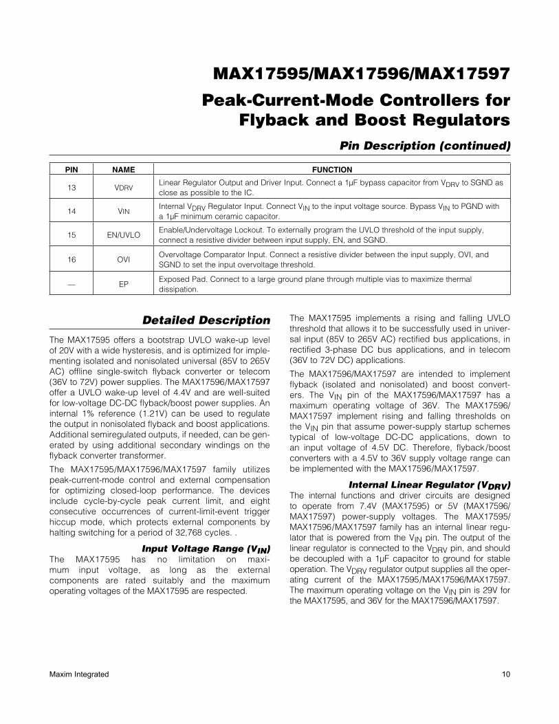
PIN NAME FUNCTION
13 VDRVLinear Regulator Output and Driver Input. Connect a 1µF bypass capacitor from VDRV to SGND as close as possible to the IC.
14 VINInternal VDRV Regulator Input. Connect VIN to the input voltage source. Bypass VIN to PGND with a 1FF minimum ceramic capacitor.
15 EN/UVLOEnable/Undervoltage Lockout. To externally program the UVLO threshold of the input supply, connect a resistive divider between input supply, EN, and SGND.
16 OVIOvervoltage Comparator Input. Connect a resistive divider between the input supply, OVI, and SGND to set the input overvoltage threshold.
— EPExposed Pad. Connect to a large ground plane through multiple vias to maximize thermal dissipation.
MAX17595/MAX17596/MAX17597
Peak-Current-Mode Controllers for Flyback and Boost Regulators
11Maxim Integrated
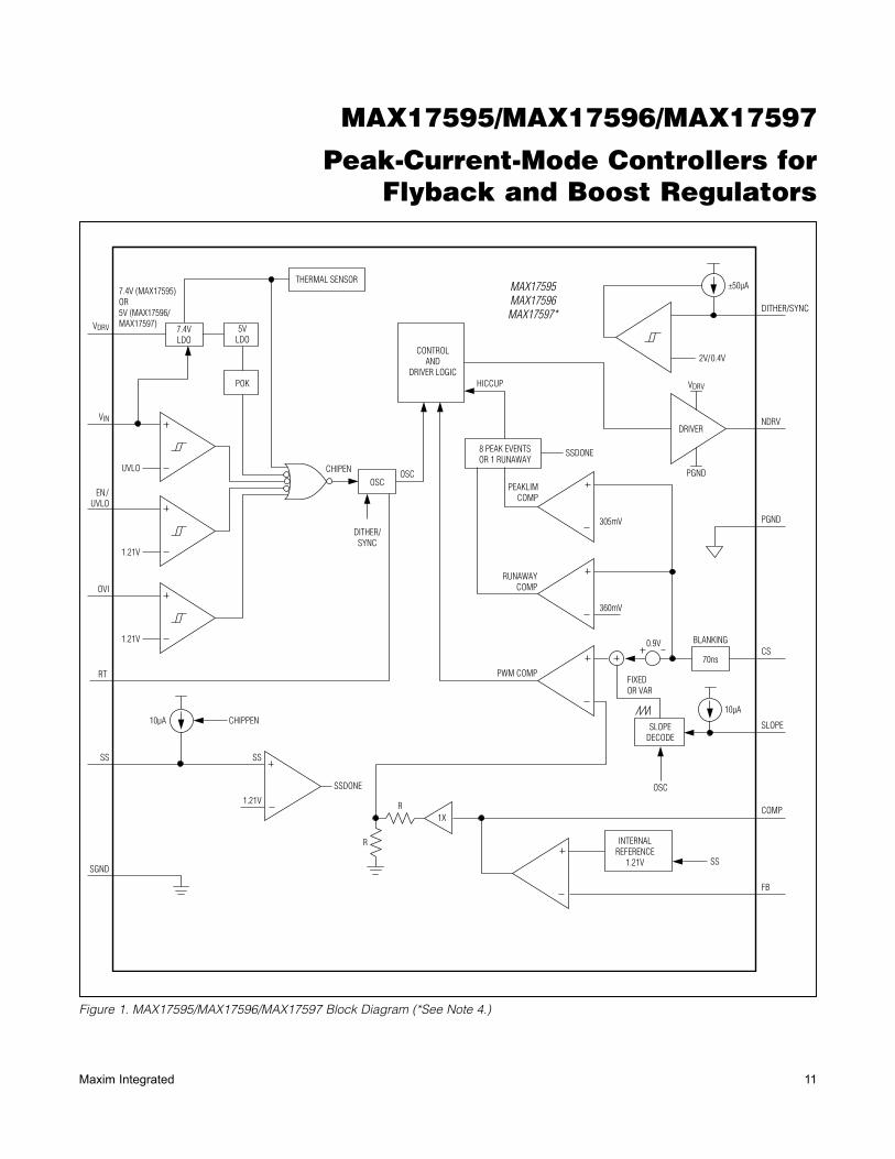
Figure 1. MAX17595/MAX17596/MAX17597 Block Diagram (*See Note 4.)
CONTROLAND
DRIVER LOGICHICCUP
8 PEAK EVENTSOR 1 RUNAWAY
SSDONE
SS
SS
SSDONE
1.21V
CHIPPEN
DITHER/SYNC
1.21V
1.21V
UVLO
VDRV
DITHER/SYNC
NDRV
PGND
CS
SLOPE
COMP
FB
VIN
EN/UVLO
OVI
RT
SS
SGND
7.4V (MAX17595)OR5V (MAX17596/MAX17597)
OSC
PEAKLIMCOMP
305mV
360mV
FIXEDOR VAR
10µA10µA
±50µA
RUNAWAYCOMP
PWM COMP
OSCOSC
70ns
BLANKING
R
R
INTERNALREFERENCE
1.21V
1X
DRIVER
VDRV
2V/0.4V
PGND
SLOPEDECODE
0.9V
5VLDO
POK
MAX17595MAX17596MAX17597*
7.4VLDO
THERMAL SENSOR
CHIPEN
MAX17595/MAX17596/MAX17597
Peak-Current-Mode Controllers for Flyback and Boost Regulators
12Maxim Integrated
n-Channel MOSFET Gate Driver (NDRV)The devices offer a built-in gate driver for driving an external n-channel MOSFET. The NDRV pin can source/sink peak currents in excess of 900mA/1500mA.
Maximum Duty CycleThe MAX17595/MAX17596 operate at a maximum duty cycle of 49%. The MAX17597 offers a maximum duty cycle of 94% to implement flyback and boost converters involving large input-to-output voltage ratios in DC-DC applications. Slope compensation is necessary for sta-ble operation of peak-current-mode controlled convert-ers such as the MAX17595/MAX17596/MAX17597, in addition to the loop compensation required for small signal stability. The MAX17595/MAX17596/MAX17597 implement a SLOPE pin for this purpose. See the Slope Compensation section for more details.
Soft-Start (SS)The devices implement soft-start operation for the fly-back/boost regulators. A capacitor connected to the SS pin programs the soft-start period. The soft-start feature reduces input inrush current during startup. When the voltage on the SLOPE pin is more than 0.2V, the refer-ence to the internal error amplifier is ramped up from 0V to 1.21V in a linear manner, as programmed by the soft-start capacitor. See the Programming Soft-Start (SS) (SS) section.
Switching Frequency Selection (RT)The ICs’ switching frequency is programmable between 100kHz and 1MHz with resistor RRT connected between RT and SGND. Use the following formula to determine the appropriate value of RRT needed to generate the desired output-switching frequency (fSW):
=10
RTSW
10R
f
where fSW is the desired switching frequency.
Frequency Dithering for Spread-Spectrum Applications (Low EMI)
The switching frequency of the converter can be dithered in a range of Q10% by connecting a capaci-tor from DITHER/SYNC to SGND, and a resistor from DITHER to RT. Spread-spectrum modulation technique spreads the energy of switching frequency and its har-monics over a wider band while reducing their peaks, helping to meet stringent EMI goals.
Applications Information
Startup Voltage and Input Overvoltage Protection Setting (EN/UVLO, OVI)
The devices’ EN/UVLO pin serves as an enable/disable input, as well as an accurate programmable input UVLO pin. The devices do not commence startup operation unless the EN/UVLO pin voltage exceeds 1.21V (typ). The devices turn off if the EN/UVLO pin voltage falls below 1.15V (typ). A resistor-divider from the input DC bus to ground can be used to divide down and apply a fraction of the input DC voltage (VDC) to the EN/UVLO pin. The values of the resistor-divider can be selected so the EN/UVLO pin voltage exceeds the 1.23V (typ) turn-on threshold at the desired input DC bus voltage. The same resistor-divider can be modified with an additional resistor (ROVI) to implement input overvoltage protec-tion in addition to the EN/UVLO functionality as shown in Figure 2. When voltage at the OVI pin exceeds 1.21V (typ), the devices stop switching and resume switching opera tions only if voltage at the OVI pin falls below 1.15V (typ). For given values of startup DC input voltage (VSTART) and input overvoltage-protection voltage (VOVI), the resistor values for the divider can be calculated as fol lows, assuming a 24.9kI resistor for ROVI:
OVIEN OVI
START
VR R 1 k
V
= × −
I
where ROVI is in kI, while VSTART and VOVI are in volts.
STARTSUM OVI EN
VR R R 1 k
1.21
= + × −
I
where REN and ROVI are in kI, while VSTART is in volts.
In universal AC input applications, RSUM may need to be implemented as equal resistors in series (RDC1, RDC2, and RDC) so that voltage across each resistor is limited to its maximum operation voltage.
= = = SUMDC1 DC2 DC3
RR R R k
3I
For low-voltage DC-DC applications based on the MAX17596/MAX17597, a single resistor can be used in the place of RSUM, as the voltage across it is approxi-mately 40V.

MAX17595/MAX17596/MAX17597
Peak-Current-Mode Controllers for Flyback and Boost Regulators
13Maxim Integrated
Figure 2. Programming EN/UVLO and OVI
Startup OperationThe MAX17595 is optimized for implementing an offline single-switch flyback converter and has a 20V VIN UVLO wake-up level with hysteresis of 15V (min). In offline applications, a simple cost-effective RC startup circuit is used. When the input DC voltage is applied, the startup resistor (RSTART) charges the startup capacitor (CSTART), causing the voltage at the VIN pin to increase towards the wake-up VIN UVLO threshold (20V typ). During this time, the MAX17595 draws a low startup current of 20FA (typ) through RSTART. When the voltage at VIN reaches the wake-up VIN UVLO threshold, the MAX17595 commenc-es switching and control operations. In this condition, the MAX17595 draws 2mA (typ) current from CSTART for its internal operation. In addition, the gate-drive current is also drawn from CSTART, which is a function of the gate charge of the external MOSFET used and switching fre-quency. Since this total current cannot be supported by the current through RSTART, the voltage on CSTART starts to drop. When suitably configured, as shown in Figure 3, the external MOSFET is switched by the NDRV pin and the flyback converter generates pulses on bias winding NB. The soft-start period of the con-verter should be programmed so the bias winding pulses sustain the voltage on CSTART before it falls below 7V, thus allowing continued operation. The large hysteresis of the MAX17595 allows for a small startup capacitor (CSTART). The low startup current (20FA typ) allows the use of a large startup resistor (RSTART), thus reducing power dissipation at higher DC bus voltages. RSTART might need to be implemented as equal, multiple resistors in series (RIN1, RIN2, and RIN3) to share the applied high DC voltage in offline applications so that the voltage across each resistor is limited to its maximum continuous operating voltage rating. RSTART and CSTART can be calculated as:
+ × × = µ× × + ×
VDRV IN SS
START SS G SW6
C I t 0.1
C 0.75 Ft Q f0.04
10
where IIN is the supply current drawn at the VIN pin in mA, QG is the gate charge of the external MOSFET used in nC, fSW is the switching frequency of the converter in Hz, and tSS is the soft-start time programmed for the fly-back converter in ms. CVDRV is a cummulative capacitor used in VDRV node in μF. See the Programming Soft-Start of Flyback/Boost Converter (SS) section.
( )STARTSTART
START
V 10 50R k
1 C
− ×=
+ I
where CSTART is the startup capacitor in FF.
For designs that cannot accept power dissipation in the startup resistors at high DC input voltages in offline appli-cations, the startup circuit can be set up with a current source instead of a startup resistor as shown in Figure 4.
The startup capacitor (CSTART) can be calculated using the above equation:
Resistors RSUM and RISRC can be calculated as:
STARTSUM
BEQ1ISRC
VR M
10V
R M70
= W
= W
The VIN UVLO wake-up threshold of the MAX17596/MAX17597 is set to 4.1V (typ) with a 200mV hyster esis, optimized for low-voltage DC-DC applications down to 4.5V. For applications where the input DC voltage is low enough (e.g., 4.5V to 5.5V DC) that the power loss incurred to supply the operating current of the MAX17596/MAX17597 can be tolerated, the VIN pin is directly connected to the DC input, as shown in Figure 5. In the case of higher DC input voltages (e.g., 16V to 32V DC), a startup circuit, such as that shown in Figure 6, can be used to minimize power dissipation. In this startup
OVI
RDC1
RSUM RDC2
RDC3
EN/UVLO
REN
ROVI
MAX17595MAX17596MAX17597

MAX17595/MAX17596/MAX17597
Peak-Current-Mode Controllers for Flyback and Boost Regulators
14Maxim Integrated
scheme, the transistor (Q1) supplies the switching cur-rent until a bias winding NB comes up and turns off Q1. The resistor (RZ) can be calculated as:
−= × WZ INMINR 2 (V 6.3) k
Programming Soft-Start (SS)The soft-start period for the devices can be programmed by selecting the value of the capacitor CSS connected
from the SS pin to SGND. Capacitor CSS can be calcu-lated as:
SS SSC 8.2645 t nF= ×
where tSS is expressed in ms. This equation is directly applicable to the boost converter application circuit of Figure 11. For optoisolated converters, the soft-start period is approximately equal to 30% of tSS when the
Figure 3. MAX17595 RC-Based Startup Circuit
Figure 4. MAX17595 Current-Source-Based Startup Circuit
VDRV
VDC
COUT
VIN
VOUT
CVDRV
CSTART
LDO DRVCS
NDRV
D1D2
NSNP
NB
MAX17595
VDC
RIN1
RSTART RIN2
RIN3
RIN1
VDC
RSUM RIN2
VDRV
VDC
COUT
D1
VIN
RISRC
VOUT
CVDRVRS
CSTART
RIN3
LDO DRV CS
NDRV
D2
NSNP
NB
MAX17595

MAX17595/MAX17596/MAX17597
Peak-Current-Mode Controllers for Flyback and Boost Regulators
15Maxim Integrated
error amplifier is set up as a proportional gain amplifier as shown in Figure 9.
Programming Output VoltageThe devices incorporate an error amplifier with a 1% pre-cision voltage reference that enables negative feedback control of the output voltage. The output voltage of the switching converter can be programmed by selecting the values for the resistor-divider connected from VOUT, and the flyback/boost output to ground, with the midpoint of the divider connected to the FB pin (Figure 7). With RB
selected in the 20kI to 50kI range, RU can be calcu-lated as:
OUTU B B
VR R 1 k , whereR is in k .
1.21
= × −
I I
Peak-Current-Limit Setting (CS)The devices include a robust overcurrent protection scheme that protects the device under overload and short-circuit conditions. A current-sense resistor, connected between the source of the MOSFET and PGND, sets the peak current limit. The current-limit comparator has a voltage
Figure 6. MAX17596/MAX17597 Typical Startup Circuit with Bias Winding to Turn Off Q1 and Reduce Power Dissipation
Figure 5. MAX17596/MAX17597 Typical Startup Circuit with VIN Connected Directly to DC Input
VDRV
VDC
COUTCDRV
Np Ns
D1
VINVIN
VOUT
RS
CS
NDRV
LDO
MAX17596MAX17597
DRV
VDRV
VDC
COUTCDRV
Np
NB
Ns
D1
VIN
VIN
RZ
ZD16.3V
CIN
RS
CS
NDRV
MAX17596MAX17597
LDOQ1
DRV
D2

MAX17595/MAX17596/MAX17597
Peak-Current-Mode Controllers for Flyback and Boost Regulators
16Maxim Integrated
trip level (VCS-PEAK) of 300mV. Use the following equa-tion to calculate the value of RCS:
CSMOSFET
300mVR
I= I
where IMOSFET is the peak current flowing through the MOSFET.
The devices implement 65ns of leading-edge blank-ing to ignore leading-edge current spikes. Use a small RC network for additional filtering of the lead-ing edge spike on the sense waveform when need-ed. Set the corner frequency between 10MHz and 20MHz. After the leading-edge blanking time, the device monitors VCS. The switching cycle is termi-nated within 30ns from VCS exceeding 300mV.
The devices offer a runaway current limit scheme that protects the devices under high-input-voltage short-circuit conditions when there is insufficient output volt-age available to restore inductor current built up during the on period of the flyback/boost converter. Either eight consecutive occurrences of the peak-current-limit event or one occurrence of the runaway current limit trigger a hiccup mode that protects the converter by immediately suspending switching for a period of time (tRSTART). This allows the overload current to decay due to power loss in the converter resistances, load, and the output diode of the flyback/boost converter before soft-start is attempted again. The runaway current limit is set at a VCS-PEAK of 360mV (typ). The peak-current-limit- triggered hiccup operation is disabled until the end of the soft-start period, while the runaway current-limit- triggered hiccup operation is always enabled.
Programming Slope Compensation (SLOPE)
The MAX17595/MAX17596 operate at a maximum duty cycle of 49%. In theory, they do not require slope compensation to prevent subharmonic instability that occurs naturally in continuous-conduction mode (CCM) peak-current-mode-controlled converters operating at duty cycles greater than 50%. In practice, the MAX17595/MAX17596 require a minimum amount of slope compen-sation to provide stable operation. The devices allow the user to program this default value of slope compensation simply by leaving the SLOPE pin unconnected. It is rec-ommended that discontinuous-mode designs also use this minimum amount of slope compensation to provide better noise immunity and jitter-free operation.
The MAX17597 flyback/boost converter can be designed to operate in either discontinuous-conduction mode (DCM) or to enter into continuous-conduction mode at a specific load condition for a given DC input voltage. In continuous-conduction mode, the flyback/ boost converter needs slope compensation to avoid subharmonic instability that occurs naturally over all specified load and line conditions in peak-current-mode-controlled converters operating at duty cycles greater than 50%. A minimum amount of slope signal is added to the sensed current signal even for converters operating below 50% duty to provide stable, jitter-free operation. The SLOPE pin allows the user to program the necessary slope compensation by setting the value of the resistor (RSLOPE) connected from the SLOPE pin to ground.
ESLOPE
S 8R k
1.55
−= I
where the slope (SE) is expressed in mV/Fs.
Frequency Dithering for Spread-Spectrum Applications (Low EMI)
The switching frequency of the converter can be dithered in a range of Q10% by connecting a capacitor from DITHER/SYNC to SGND, and a resistor from DITHER to RT as shown in the Typical Operating Circuits. This results in lower EMI.
A current source at DITHER/SYNC charges capacitor CDITHER to 2V at 50FA. Upon reaching this trip point, it discharges CDITHER to 0.4V at 50FA. The charging and discharging of the capacitor generates a triangular wave-form on DITHER/SYNC with peak levels at 0.4V and 2V and a frequency that is equal to:
=×TRI
DITHER
50 Af
C 3.2V
F
Figure 7. Programming Output Voltage
FB
RU
RB
VOUT
MAX17595MAX17596MAX17597

MAX17595/MAX17596/MAX17597
Peak-Current-Mode Controllers for Flyback and Boost Regulators
17Maxim Integrated
typically, fTRI should be set close to 1kHz. Resistor RDITHER connected from DITHER/SYNC to RT deter-mines the amount of dither as follows:
RT
DITHER
R%DITHER
R=
where %DITHER is the amount of dither expressed as a percentage of the switching frequency. Setting RDITHER to 10 x RRT generates Q10% dither.
Synchronization (SYNC)The internal oscillator can be synchronized to an exter-nal clock by applying the clock to the DITHER/SYNC pin directly. The external clock frequency can be set any-where between 1.1x and 1.8x times the programmable switching frequency for the MAX17595/MAX17596. The synchronization feature is not available in the MAX17597. An external clock increases the maximum duty cycle by a factor of (fSYNC / fSW).
Error Amplifier and Loop CompensationThe MAX17595/MAX17596/MAX17597 include an inter-nal transconductance error amplifier. The noninverting input of the error amplifier is internally connected to the internal reference and the inverting input is brought out at the FB pin to apply the feedback signal. The internal reference is linearly ramped up from 0V to 1.21V (typ) when the device is enabled at turn-on. After soft-start, the internal reference is connected to the bandgap.
In isolated applications, where an optocoupler is used to transmit the control signal from the secondary side, the emitter current of the optocoupler flows through a resis-tor to ground to set up the feedback voltage. A shunt regulator is usually employed as a secondary-side error amplifier to drive the optocoupler photodiode to couple the control signal to the primary. The loop compensation is applied in the secondary side as an R-C network on the shunt regulator. The MAX17595/MAX17596/MAX17597 error amp can be set up as a proportional gain ampli-fier, or used to implement additional poles or zeros. The Typical Application Circuits for the MAX17595/MAX17596 use the internal error amplifier as a propor-tional gain amplifier.
In nonisolated applications, the output voltage is divided down with a voltage-divider to ground and is applied to the FB pin. Loop compensation is applied at the COMP pin as an R-C network from COMP to GND that imple-ments the required poles and zeros, as shown in Figure
8. The boost converter application circuit of Figure 11 for the MAX17597 uses this approach.
Layout, Grounding and BypassingAll connections carrying pulsed currents must be very short and as wide as possible. The inductance of these connections must be kept to an absolute minimum due to the high di/dt of the currents in high-frequency-switching power converters. This implies that the loop areas for forward and return pulsed currents in various parts of the circuit should be minimized. Additionally, small current loop areas reduce radiated EMI. Similarly, the heatsink of the MOSFET presents a dV/dt source; therefore, the surface area of the MOSFET heatsink should be minimized as much as possible.
Ground planes must be kept as intact as possible. The ground plane for the power section of the converter should be kept separate from the analog ground plane, except for a connection at the least noisy section of the power ground plane, typically the return of the input filter capacitor. The negative terminal of the filter capacitor, the ground return of the power switch and current-sensing resistor, must be close together. PCB layout also affects the thermal performance of the design. A number of thermal vias that connect to a large ground plane should be provided under the exposed pad of the part for efficient heat dissipation. For a sample layout that ensures first-pass success, refer to the MAX17595 evalu-ation kit layout available at www.maximintegrated.com. For universal AC input designs, follow all applicable safety regulations. Offline power supplies can require UL, VDE, and other similar agency approvals.
Figure 8. Error-Amplifier Compensation Network
COMP
RZ
CZ
CP
MAX17595MAX17596MAX17597

MAX17595/MAX17596/MAX17597
Peak-Current-Mode Controllers for Flyback and Boost Regulators
18Maxim Integrated
Typical Operating Circuits
Figure 9. MAX17595 Typical Application Circuit (Universal Offline Isolated Power Supply)
N1
VIN
1
2
R264.99kI
R282.49kI
R29221I
R22470I
C81µF
C111000pF
R210.2I
R20100I
VFB
VDRV
IN
VOUT
C1768nF
SGND
U3
EP
SGND
SGND
SGND
SGND
MAX17595
SGND PGND
C21470nF
R4549kI
R3549kI
R2549kI
R110IAC1
AC2
C10.1µF/
275V AC
R519.8kI
R64.99kI
R1249.9kI
VFB
VIN
COMP
SGND
DITHER /SYNC
R14402kI
R15402kI
R16402kI
C7100nF
C5100µF450V
C94.7µF50V
C103300pF
R18100kI
L16.8mH
D1
C60.47µF
R1910I
PGND
PGND
PGNDVIN
IN VOUT
VOUT
GND0
T1D2
D3
D4
C1322µF
C1422µF
C1522µF
C1622µF
R982.5kI
RT
SLOPE
NDRV
PGND
PGND
SGND
CS
VDRV
VDRV
SS
FB
EN/UVLO
OVI
C456pFR13
22kI
15V, 1.5A
SGND

MAX17595/MAX17596/MAX17597
Peak-Current-Mode Controllers for Flyback and Boost Regulators
19Maxim Integrated
Typical Operating Circuits (continued)
Figure 10. MAX17596 Typical Application Circuit (Power Supply for DC-DC Applications)
N1
R8100I
R950mI
R148.6kI
R1616.5kI
R158.6kI
R1210kI
R17470I
R13470I
C140.1µF
VFB
VDRV
VOUTC6300pF
C1522nF
C17500nF
GND0
C1656pFU2
U3
NDRV
EP
VIN
SS
SLOPE
FB
COMP
PGND
C5100nF
C30.22µF
C24.7µF
50V
C147µF63V
PGND
VIN VOUT
GND0
24V, 1.5AOUTPUT
18V TO 36V
R710kI
R620kI
R5348kI
R449.9kI
R322kI
R1750I
C40.1µF, 50V
C910µF50V
C1110µF50V
C1210µF50V
D1
VFB
EN /UVLO
OVI
VIN
VIN
R1028.5kI
RT
SGND
CS
DITHER/SYNC
MAX17596U1
C1010µF50V
C1310µF50V
PGNDSGNDSGND
C71µF
VDRV
VDRV
C8100nF
D2T1
VOUT
MAX17595/MAX17596/MAX17597
Peak-Current-Mode Controllers for Flyback and Boost Regulators
20Maxim Integrated
Typical Operating Circuits (continued)
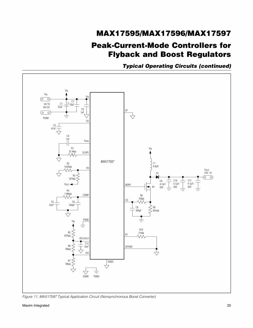
Figure 11. MAX17597 Typical Application Circuit (Nonsynchronous Boost Converter)
EP
VIN
L16.8µH
C94.7µF/50VN1
R8100I
R41.96kI
R3187kI
R29.92kI
R132.4kI
R1021kI
R718kI
R618kI
R5187kI
R965mI
C8300pF
VOUT24V, 1A
VOUT
D1
NDRV
CS
RT
DITHER
SGND
SGND PGND
OVI
EN /UVLO
PGND
COMP
FB
SLOPE
VDRV
VIN
SS
C6330pF
C533nF
C41µF
C347nF
PGND
8V TO14V DC
VIN
VIN
C710µFC1
22µF
VIN
MAX17597
C21µF
C104.7µF/50V
C114.7µF/50V
C1210nF

MAX17595/MAX17596/MAX17597
Peak-Current-Mode Controllers for Flyback and Boost Regulators
21Maxim Integrated
Package Information
For the latest package outline information and land patterns (footprints), go to www.maximintegrated.com/packages. Note that a “+”, “#”, or “-” in the package code indicates RoHS status only. Package drawings may show a different suffix character, but the drawing pertains to the package regardless of RoHS status.
Ordering Information/Selector Guide
+Denotes a lead(Pb)-free/RoHS-compliant package.*Exposed pad.
PACKAGE TYPE PACKAGE CODE OUTLINE NO. LAND PATTERN NO.
16 TQFN T1633+4 21-0136 90-0032
PARTTEMP
RANGEPIN
PACKAGEFUNCTIONALITY
UVLO, VIN CLAMP
DMAX
MAX17595ATE+ -40NC to +125NC 16 TQFN-EP* Offline Flyback Controller 20V, Yes 46%
MAX17596ATE+ -40NC to +125NC 16 TQFN-EP* Low-Voltage DC-DC Flyback Controller 4V, No 46%
MAX17597ATE+ -40NC to +125NC 16 TQFN-EP* Boost Controller 4V, No 93%
MAX17595/MAX17596/MAX17597
Peak-Current-Mode Controllers for Flyback and Boost Regulators
Maxim Integrated cannot assume responsibility for use of any circuitry other than circuitry entirely embodied in a Maxim Integrated product. No circuit patent licenses are implied. Maxim Integrated reserves the right to change the circuitry and specifications without notice at any time. The parametric values (min and max limits) shown in the Electrical Characteristics table are guaranteed. Other parametric values quoted in this data sheet are provided for guidance.
Maxim Integrated 160 Rio Robles, San Jose, CA 95134 USA 1-408-601-1000 22© 2015 Maxim Integrated Products, Inc. Maxim Integrated and the Maxim Integrated logo are trademarks of Maxim Integrated Products, Inc.
Revision History
REVISIONNUMBER
REVISIONDATE
DESCRIPTIONPAGES
CHANGED
0 1/12 Initial release —
1 2/13Updated General Description, Electrical Characteristics tables, Typical Operating Characteristics; Detailed Description, Figures 1, 3–6; Typical Operating Circuits, deleted sections relating to soft-stop, flyback, and boost.
1–22
2 6/13 Updated Pin Description for EP and Figure 10 10, 19
3 11/14 Deleted automotive reference in Applications section 1
4 5/15 Updated Benefits and Features section 1