LTC4367 - 100V Overvoltage, Undervoltage and Reverse Supply ...
22
LTC4367 1 4367fa For more information www.linear.com/LTC4367 TYPICAL APPLICATION FEATURES DESCRIPTION 100V Overvoltage, Undervoltage and Reverse Supply Protection Controller 24V Automotive Application with +100V, –40V Protection APPLICATIONS n Wide Operating Voltage Range: 2.5V to 60V n Overvoltage Protection to 100V n Reverse Supply Protection to –40V n LTC4367: Blocks 50Hz and 60Hz AC Power n LTC4367: 32ms Recovery from Fault n LTC4367-1: Fast 500µs Recovery from Fault n No Input Capacitor or TVS Required for Most Applications n Adjustable Undervoltage and Overvoltage Thresholds n Controls Back-to-Back N-Channel MOSFETs n Low Operating Current: 70µA n Low Shutdown Current: 5µA n 8-Pin MSOP and 3mm × 3mm DFN Packages n Portable Instrumentation n Industrial Automation n Laptops n Automotive Surge (Load Dump) Protection L, LT, LTC, LTM, Linear Technology and the Linear logo are registered trademarks and ThinSOT is a trademark of Linear Technology Corporation. All other trademarks are the property of their respective owners. Load Protected from Reverse and Overvoltage at V IN The LTC ® 4367 protects applications where power sup- ply input voltages may be too high, too low or even negative. It does this by controlling the gate voltages of a pair of external N-channel MOSFETs to ensure that the output stays within a safe operating range.The LTC4367 withstands voltages between –40V and 100V and has an operating range of 2.5V to 60V, while consuming only 70µA in normal operation. Two comparator inputs allow configuration of the over- voltage (OV) and undervoltage (UV) set points using an external resistive divider. A shutdown pin provides external control for enabling and disabling the MOSFETs as well as placing the device in a low current shutdown state. A fault output indicates that the GATE pin is pulling low when the part is in shutdown or the input voltage is outside the UV and OV set points. The LTC4367 has a 32ms turn-on delay that debounces live connections and blocks 50Hz to 60Hz AC power. For fast recovery after faults, the LTC4367-1 has a reduced turn-on delay of 500µs. VALID WINDOW V IN V IN V OUT V OUT OV = 36V UV = 7V 200ms/DIV –40V 20V/DIV GND 4367 TA01b +70V 20V/DIV V IN UV OV SHDN OV = 36V UV = 7V 4367 TA01a V OUT FAULT GATE V IN 24V V OUT 2A Si7942 GND LTC4367 1500k 121k 29.4k 464k
Transcript of LTC4367 - 100V Overvoltage, Undervoltage and Reverse Supply ...

LTC4367
14367fa
For more information www.linear.com/LTC4367
Typical applicaTion
FeaTures DescripTion
100V Overvoltage, Undervoltage and Reverse
Supply Protection Controller
24V Automotive Application with +100V, –40V Protection
applicaTions
n Wide Operating Voltage Range: 2.5V to 60V n Overvoltage Protection to 100V n Reverse Supply Protection to –40V n LTC4367: Blocks 50Hz and 60Hz AC Power n LTC4367: 32ms Recovery from Fault n LTC4367-1: Fast 500µs Recovery from Fault n No Input Capacitor or TVS Required for Most
Applications n Adjustable Undervoltage and Overvoltage Thresholds n Controls Back-to-Back N-Channel MOSFETs n Low Operating Current: 70µA n Low Shutdown Current: 5µA n 8-Pin MSOP and 3mm × 3mm DFN Packages
n Portable Instrumentation n Industrial Automation n Laptops n Automotive Surge (Load Dump) Protection
L, LT, LTC, LTM, Linear Technology and the Linear logo are registered trademarks and ThinSOT is a trademark of Linear Technology Corporation. All other trademarks are the property of their respective owners.
Load Protected from Reverse and Overvoltage at VIN
The LTC®4367 protects applications where power sup-ply input voltages may be too high, too low or even negative. It does this by controlling the gate voltages of a pair of external N-channel MOSFETs to ensure that the output stays within a safe operating range.The LTC4367 withstands voltages between –40V and 100V and has an operating range of 2.5V to 60V, while consuming only 70µA in normal operation.
Two comparator inputs allow configuration of the over-voltage (OV) and undervoltage (UV) set points using an external resistive divider. A shutdown pin provides external control for enabling and disabling the MOSFETs as well as placing the device in a low current shutdown state. A fault output indicates that the GATE pin is pulling low when the part is in shutdown or the input voltage is outside the UV and OV set points.
The LTC4367 has a 32ms turn-on delay that debounces live connections and blocks 50Hz to 60Hz AC power. For fast recovery after faults, the LTC4367-1 has a reduced turn-on delay of 500µs.
VALID WINDOW
VIN
VIN
VOUTVOUT
OV = 36VUV = 7V
200ms/DIV
–40V20V/DIV
GND
4367 TA01b
+70V20V/DIV
VIN
UV
OV
SHDN
OV = 36VUV = 7V
4367 TA01a
VOUT
FAULT
GATE
VIN24V
VOUT2A
Si7942
GND
LTC4367
1500k
121k
29.4k
464k

LTC4367
24367fa
For more information www.linear.com/LTC4367
absoluTe MaxiMuM raTings
Supply Voltage VIN ........................................................ –40V to 100VInput Voltages (Note 3) UV, SHDN .............................................. –0.3V to 80V OV ............................................................ –0.3V to 5V VOUT....................................................... –0.3V to 80VOutput Voltages FAULT ..................................................... –0.3V to 80V GATE (Note 4) ......................................... –40V to 75V
TOP VIEW
DD PACKAGE8-LEAD (3mm × 3mm) PLASTIC DFN
5
6
7
8
9
4
3
2
1 GATE
VOUT
FAULT
SHDN
VIN
UV
OV
GND
EXPOSED PAD (PIN 9) PCB GROUND CONNECTION OPTIONAL TJMAX = 150°C, θJA = 43°C/W, θJC = 5.5°C/W
1234
VINUVOV
GND
8765
GATEVOUTFAULTSHDN
TOP VIEW
MS8 PACKAGE8-LEAD PLASTIC MSOP
TJMAX = 150°C, θJA = 160°C/W
Input Currents SHDN, UV .........................................................–1mA OV ......................................................................–1mAOperating Ambient Temperature Range LTC4367C ................................................ 0°C to 70°C LTC4367I .............................................–40°C to 85°C LTC4367H .......................................... –40°C to 125°CStorage Temperature Range .................. –65°C to 150°CLead Temperature (Soldering, 10sec)
for MSOP Only .................................................. 300°C
(Note 1, Note 2)
pin conFiguraTion
LTC4367
34367fa
For more information www.linear.com/LTC4367
LEAD FREE FINISH TAPE AND REEL PART MARKING* PACKAGE DESCRIPTION TEMPERATURE RANGE
LTC4367CDD#PBF LTC4367CDD#TRPBF LGTF 8-Lead (3mm × 3mm) Plastic DFN 0°C to 70°C
LTC4367CDD-1#PBF LTC4367CDD-1#TRPBF LGVW 8-Lead (3mm × 3mm) Plastic DFN 0°C to 70°C
LTC4367IDD#PBF LTC4367IDD#TRPBF LGTF 8-Lead (3mm × 3mm) Plastic DFN –40°C to 85°C
LTC4367IDD-1#PBF LTC4367IDD-1#TRPBF LGVW 8-Lead (3mm × 3mm) Plastic DFN –40°C to 85°C
LTC4367HDD#PBF LTC4367HDD#TRPBF LGTF 8-Lead (3mm × 3mm) Plastic DFN –40°C to 125°C
LTC4367HDD-1#PBF LTC4367HDD-1#TRPBF LGVW 8-Lead (3mm × 3mm) Plastic DFN –40°C to 125°C
LTC4367CMS8#PBF LTC4367CMS8#TRPBF LTGTD 8-Lead Plastic MSOP 0°C to 70°C
LTC4367CMS8-1#PBF LTC4367CMS8-1#TRPBF LTGVX 8-Lead Plastic MSOP 0°C to 70°C
LTC4367IMS8#PBF LTC4367IMS8#TRPBF LTGTD 8-Lead Plastic MSOP –40°C to 85°C
LTC4367IMS8-1#PBF LTC4367IMS8-1#TRPBF LTGVX 8-Lead Plastic MSOP –40°C to 85°C
LTC4367HMS8#PBF LTC4367HMS8#TRPBF LTGTD 8-Lead Plastic MSOP –40°C to 125°C
LTC4367HMS8-1#PBF LTC4367HMS8-1#TRPBF LTGVX 8-Lead Plastic MSOP –40°C to 125°C
Consult LTC Marketing for parts specified with wider operating temperature ranges. *The temperature grade is identified by a label on the shipping container.For more information on lead free part marking, go to: http://www.linear.com/leadfree/ For more information on tape and reel specifications, go to: http://www.linear.com/tapeandreel/. Some packages are available in 500 unit reels through designated sales channels with #TRMPBF suffix.
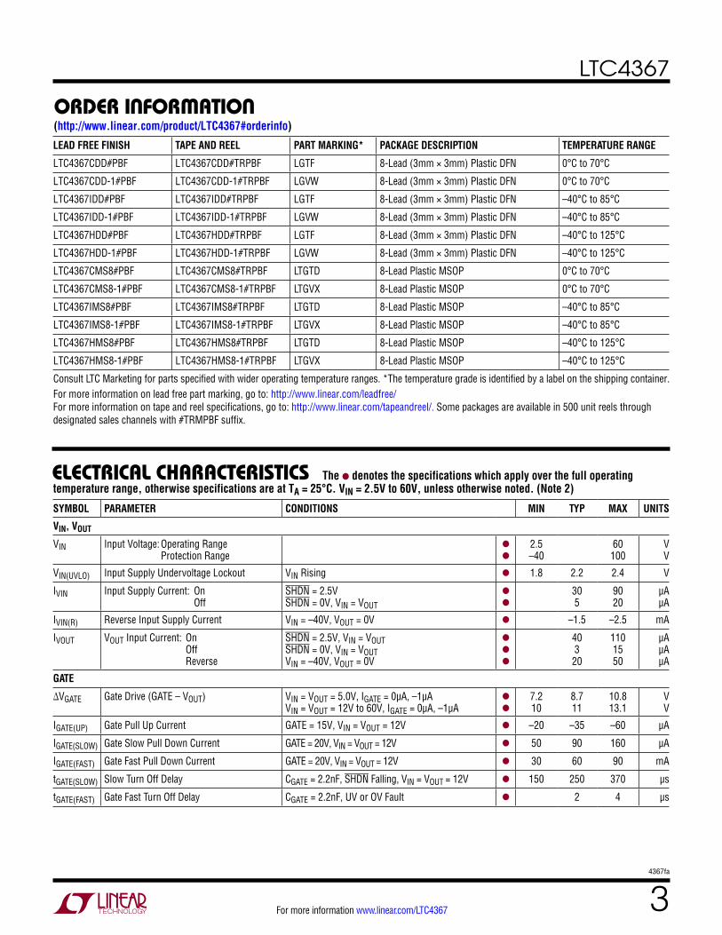
elecTrical characTerisTics
SYMBOL PARAMETER CONDITIONS MIN TYP MAX UNITS
VIN, VOUT
VIN Input Voltage: Operating Range Protection Range
l
l
2.5 –40
60 100
V V
VIN(UVLO) Input Supply Undervoltage Lockout VIN Rising l 1.8 2.2 2.4 V
IVIN Input Supply Current: On Off
SHDN = 2.5V SHDN = 0V, VIN = VOUT
l
l
30 5
90 20
µA µA
IVIN(R) Reverse Input Supply Current VIN = –40V, VOUT = 0V l –1.5 –2.5 mA
IVOUT VOUT Input Current: On Off Reverse
SHDN = 2.5V, VIN = VOUT SHDN = 0V, VIN = VOUT VIN = –40V, VOUT = 0V
l
l
l
40 3
20
110 15 50
µA µA µA
GATE
ΔVGATE Gate Drive (GATE – VOUT) VIN = VOUT = 5.0V, IGATE = 0µA, –1µA VIN = VOUT = 12V to 60V, IGATE = 0µA, –1µA
l
l
7.2 10
8.7 11
10.8 13.1
V V
IGATE(UP) Gate Pull Up Current GATE = 15V, VIN = VOUT = 12V l –20 –35 –60 µA
IGATE(SLOW) Gate Slow Pull Down Current GATE = 20V, VIN = VOUT = 12V l 50 90 160 µA
IGATE(FAST) Gate Fast Pull Down Current GATE = 20V, VIN = VOUT = 12V l 30 60 90 mA
tGATE(SLOW) Slow Turn Off Delay CGATE = 2.2nF, SHDN Falling, VIN = VOUT = 12V l 150 250 370 µs
tGATE(FAST) Gate Fast Turn Off Delay CGATE = 2.2nF, UV or OV Fault l 2 4 µs
The l denotes the specifications which apply over the full operating temperature range, otherwise specifications are at TA = 25°C. VIN = 2.5V to 60V, unless otherwise noted. (Note 2)
orDer inForMaTion(http://www.linear.com/product/LTC4367#orderinfo)
LTC4367
44367fa
For more information www.linear.com/LTC4367
SYMBOL PARAMETER CONDITIONS MIN TYP MAX UNITS
tD(ON) GATE Turn-On Delay Time VIN = 12V, Power Good to ΔVGATE > 0V, CGATE = 2.2nF LTC4367 LTC4367-1
l
l
22 0.2
32 0.5
45 1.2
ms ms
UV, OV
VUV UV Input Threshold Voltage UV Falling l 492.5 500 507.5 mV
VOV OV Input Threshold Voltage OV Rising l 492.5 500 507.5 mV
VUVHYST UV Input Hysteresis VIN = VOUT = 12V l 20 25 32 mV
VOVHYST OV Input Hysteresis VIN = VOUT = 12V l 20 25 32 mV
ILEAK UV, OV Leakage Current V = 0.5V, VIN = 60V l ±10 nA
tFAULT UV, OV Fault Propagation Delay Overdrive = 50mV VIN = VOUT = 12V
l 1 2 µs
SHDN
VSHDN SHDN Input Threshold SHDN Falling l 0.4 0.75 1.2 V
ISHDN SHDN Input Current SHDN = 10V, VIN = 60V l ±15 nA
tSTART Delay Coming Out of Shutdown Mode SHDN Rising to FAULT Released, VIN = VOUT = 12V LTC4367 LTC4367-1
l 400 125
800 250
1200 500
µs µs
tSHDN(F) SHDN to FAULT Asserted VIN = VOUT = 12V l 1.5 3 µs
tLOWPWR Delay from Turn Off to Low Power Operation
VIN = VOUT = 12V LTC4367 LTC4367-1
l
l
20
0.125
32 0.3
48 0.6
ms ms
FAULT
VOL FAULT Output Voltage Low IFAULT = 500µA, VIN = 12V l 0.15 0.4 V
IFAULT FAULT Leakage Current FAULT = 5V, VIN = 60V l ±200 nA
Note 1. Stresses beyond those listed under Absolute Maximum Ratings may cause permanent damage to the device. Exposure to any Absolute Maximum Rating condition for extended periods may affect device reliability and lifetime.Note 2. All currents into pins are positive; all voltages are referenced to GND unless otherwise noted.
Note 3. These pins have a diode to GND. They may go below –0.3V if the current magnitude is limited to less than 1mA.Note 4. The GATE pin is referenced to VOUT and does not exceed 73V for the entire operating range.
elecTrical characTerisTics The l denotes the specifications which apply over the full operating temperature range, otherwise specifications are at TA = 25°C. VIN = 2.5V to 60V, unless otherwise noted. (Note 2)

LTC4367
54367fa
For more information www.linear.com/LTC4367
Typical perForMance characTerisTics
VOUT Operating Current vs Temperature
VOUT Shutdown Current vs Temperature VOUT Current vs Reverse VIN
VIN Operating Current vs Temperature
VIN Shutdown Current vs Voltage
VIN Supply Current vs Voltage (–40V to 100V)
GATE Drive vs GATE CurrentGATE Drive vs VIN Supply Voltage GATE Drive vs Temperature
VIN = 12V
VIN = 2.5V
VIN = 60V
SHDN = 2.5VVIN = VOUT
TEMPERATURE (°C)–50 –25 0 25 50 75 100 125
0
10
20
30
40
50
I VIN
(µA)
4367 G01VIN (V)
0 10 20 30 40 50 600
2
4
6
8
I VIN
(µA)
4367 G02
TA = 125°CTA = 70°CTA = 25°CTA = –45°C
SHDN = 0VVIN = VOUT
UV = SHDN = 0VVOUT = 0V
VIN (V)–50 –25 0 25 50 75 100
–2000
–1500
–1000
–500
0
500
I VIN
(µA)
4367 G03
TA = 125°CTA = 25°CTA = –45°C
VOUT = 12V
VOUT = 2.5V
VOUT = 60VSHDN = 2.5VVIN = VOUT
TEMPERATURE (°C)–50 –25 0 25 50 75 100 125
0
10
20
30
40
50
I VOU
T (µ
A)
4367 G04
VOUT = 12V
VOUT = 2.5V
VOUT = 60V
TEMPERATURE (°C)–50 –25 0 25 50 75 100 125
0
1
2
3
4
5
6
I VOU
T (µ
A)
4367 G05
SHDN = 0VVIN = VOUT
25°C
125°C
–45°CVOUT = 0V
VIN (V)0 –10 –20 –30 –40
0
5
10
15
20
I VOU
T (µ
A)
4367 G06
VIN = VOUT
VOUT = 0V
TA = 25°CIGATE = –1µA
VIN (V)0 10 20 30 40 50 60
0
4
8
12
16
∆VGA
TE (V
)
4367 G07
VIN = VOUT = 12V
VIN = VOUT = 2.5V
VIN = VOUT = 60V
IGATE = 1µA
TEMPERATURE (°C)–50 –25 0 25 50 75 100 125
0
3
6
9
12
15
∆VGA
TE (V
)
4367 G08
VIN = VOUT = 12V
IGATE(UP) (µA)0 –10 –20 –30 –40 –50 –60
0
2
4
6
8
10
12
∆VGA
TE (V
)
4367 G09
TA = 125°CTA = 25°CTA = –45°C

LTC4367
64367fa
For more information www.linear.com/LTC4367
UV/OV Propagation Delay vs Overdrive
LTC4367 GATE Turn-On Delay Time vs Temperature
LTC4367 GATE Turn-On Delay Time vs VIN
OV Threshold vs TemperatureUV/OV/SHDN Leakage vs TemperatureUV Threshold vs Temperature
Typical perForMance characTerisTics
VIN = VOUT = 12V
TEMPERATURE (°C)–50 –25 0 25 50 75 100 125
492
496
500
504
508
V UV
(mV)
4367 G10
VIN = VOUT = 12V
TEMPERATURE (°C)–50 –25 0 25 50 75 100 125
492
496
500
504
508
V OV
(mV)
4367 G11
VIN = VOUT = 60V
TEMPERATURE (°C)–50 –25 0 25 50 75 100 125
–2
0
2
4
6
8
I LEA
K (n
A)
4367 G12
SHDN = 60V
UV/OV = 0.5V
VIN = VOUT = 12VTA = 25°C
OVERDRIVE (mV)1 10 100 1k
0
10
20
30
40
50
t FAU
LT (µ
s)
4367 G13
TemperatureRecovery Delay Time vs
VIN = 12V, 60V
VIN = 2.5V
TEMPERATURE (°C)–50 –25 0 25 50 75 100 125
0
10
20
30
40
50
4367 G14
t D(O
N) (m
s)
TA = 125°C
TA = 25°C
TA = –45°C
VIN (V)0 10 20 30 40 50 60
0
10
20
30
40
50
4367 G15
t D(O
N) (m
s)
VOUT
VIN
GATE
DUAL Si79421k, 10µF LOAD ON VOUT
5ms/DIV
20V/DIV
1V/DIV
4367 G16
GND
GND GATE
VOUT
SHDN
400µs/DIV
3V/DIV
GND
5V/DIV
4367 G17
VIN = 12VDUAL Si7942 MOSFET
100µF, 12Ω LOAD
SHDN
GATE
VOUT
DUAL Si7942 MOSFET100µF, 12Ω LOAD
VIN = 12V
400µs/DIV
5V/DIV
GND
3V/DIV4367 G18
LTC4367 AC Blocking Turn-On Timing Turn-Off Timing

LTC4367
74367fa
For more information www.linear.com/LTC4367
pin FuncTionsExposed Pad: The exposed pad may be left open or con-nected to device ground.
FAULT: Fault Indication Output. This high voltage open drain output is pulled low if UV is below its monitor threshold, if OV is above its monitor threshold, if SHDN is low, or if VIN has not risen above VIN(UVLO).
GATE: Gate Drive Output for External N-channel MOSFETs. An internal charge pump provides 35µA of pull-up current and up to 13.1V of enhancement to the gate of an external N-channel MOSFET. When turned off, GATE is pulled just below the lower of VIN or VOUT. When VIN goes negative, GATE is automatically connected to VIN.
GND: Device Ground.
OV: Overvoltage Comparator Input. Connect this pin to an external resistive divider to set the desired VIN overvoltage fault threshold. This input connects to an accurate, fast (1µs) comparator with a 0.5V rising threshold and 25mV of hysteresis. When OV rises above its threshold, a 60mA current sink pulls down on the GATE output. When OV falls back below 0.475V, and after a 32ms GATE turn-on delay waiting period (500µs for LTC4367-1), the GATE charge pump is enabled. The low leakage current of the OV input allows the use of large valued resistors for the external resistive divider. Connect to GND if unused. If the voltage at the OV pin can rise above 5V, place a low leakage Zener clamp on the OV pin.
SHDN: Shutdown Control Input. SHDN high enables the GATE charge pump which in turn enhances the gate of an external N-channel MOSFET. A low on SHDN generates a pull down on the GATE output with a 90µA current sink and places the LTC4367 in low current mode (5µA). If unused, connect to VIN with a 510k resistor. If VIN goes above 80V, the SHDN pin voltage must be kept below 80V (see Applications Information).
UV: Undervoltage Comparator Input. Connect this pin to an external resistive divider to set the desired VIN undervolt-age fault threshold. This input connects to an accurate, fast (1µs) comparator with a 0.5V falling threshold and 25mV of hysteresis. When UV falls below its threshold, a 60mA current sink pulls down on the GATE output. When UV rises back above 0.525V, and after a 32ms GATE turn-on delay waiting period (500µs for LTC4367-1), the GATE charge pump is enabled. The low leakage current of the UV input allows the use of large valued resistors for the external resistive divider. If unused and VIN is less than 80V, connect to VIN with a 510k resistor.
VIN: Power Supply Input. Maximum protection range: –40V to 100V. Operating range: 2.5V to 60V.
VOUT: Output Voltage Sense Input. This pin senses the volt-age at the output side of the external N-channel MOSFET. The GATE charge pump voltage is referenced to VOUT. It is used as the charge pump input when VOUT is greater than approximately 5V.

LTC4367
84367fa
For more information www.linear.com/LTC4367
block DiagraM
VIN–40V TO 100V
5V INTERNALSUPPLY
5V INTERNALSUPPLY
LDO
2.2VUVLO
0.5V
0.5V
GND
25mVHYSTERESIS
4367 BD
IGATE35µA
REVERSEPROTECTION
CLOSES SWITCH WHEN VIN IS NEGATIVE
ENABLE
GATE PULLDOWN
FAULTOFF
TURNOFF
60mA 90µA
SHDNSHDN
GATECHARGEPUMP
f = 400kHz
VOUT
UV
OV
–
+
DELAY TIMERS
LOGIC
–
+
–
+ FAULT
GATE
LTC4367
94367fa
For more information www.linear.com/LTC4367
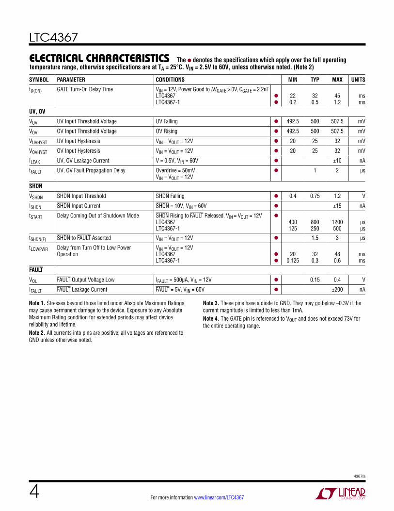
operaTionMany of today’s electronic systems get their power from external sources such as AC or wall adaptors, batteries and custom power supplies. Figure 1 shows a supply ar-rangement using a DC barrel connector. Power is supplied by an AC adaptor or, if the plug is withdrawn, by a remov-able battery. Note that the polarity of the AC adaptor and barrel connector varies by manufacturer. Trouble arises when any of the following occurs:
• The battery is installed backwards
• An AC adaptor of opposite polarity is attached
• An AC adaptor of excessive voltage is attached
• The battery is discharged below a safe level
This can lead to supply voltages that are too high, too low, or even negative. If these power sources are applied directly to the electronic systems, the systems could be subject to damage. The LTC4367 is an input voltage fault protection N-channel MOSFET controller. The part isolates an input supply from its load to protect the load from
Figure 1. Polarity Protection for DC Barrel Connectors
unexpected supply voltage conditions, while providing a low loss path for qualified power.
In the past, to protect electronic systems from improperly connected power supplies, system designers often added discrete diodes, transistors and high voltage comparators. The high voltage comparators enable system power only if the input supply falls within a desired voltage window. A Schottky diode or P-channel MOSFET typically added in series with the supply protects against reverse supply connections.
The LTC4367 provides accurate overvoltage and undervolt-age comparators to ensure that power is applied to the system only if the input supply meets the user selectable voltage window. Reverse supply protection circuits au-tomatically isolate the load from negative input voltages. During normal operation, a high voltage charge pump enhances the gate of external N-channel power MOSFETs. Power consumption is 5µA during shutdown and 70µA while operating. The LTC4367 integrates all these func-tions in 8-lead MSOP and 3mm × 3mm DFN packages.
VIN
UV
OV
SHDN
2.5V TO 60VOPERATING RANGE
4367 F01
VOUT
FAULT
GATE
GND
LTC4367
R3
–40V TO 100V PROTECTION RANGE
ACADAPTOR
INPUT
OV, UV PROTECTIONTHRESHOLDS SET TO
SATISFY LOAD CIRCUIT
R2
R1
R4
M1 M2
LOADCIRCUIT
+
–
BATTERY
LTC4367
104367fa
For more information www.linear.com/LTC4367
VOUT (V)0
0
∆VGA
TE (V
)
2
4
6
10
8
14
12
15
4367 F03
105
TA = 25°CIGATE = –1µA
VIN = 60V
VIN = 12V
VIN = 5V
VIN = 2.5V
VIN = 3.3V
applicaTions inForMaTionThe LTC4367 is an N-channel MOSFET controller that protects a load from faulty supply connections. A basic application circuit using the LTC4367 is shown in Figure 2 The circuit provides a low loss connection from VIN to VOUT as long as the voltage at VIN is between 3.5V and 18V. Voltages at VIN outside of the 3.5V to 18V range are prevented from getting to the load and can be as high as 100V and as low as –40V. The circuit of Figure 2 protects against negative voltages at VIN as shown. No other external components are needed.
During normal operation, the LTC4367 provides up to 13.1V of gate enhancement to the external back-to-back N-channel MOSFETs. This turns on the MOSFETs, thus connecting the load at VOUT to the supply at VIN.
GATE Drive
The LTC4367 turns on the external N-channel MOSFETs by driving the GATE pin above VOUT. The voltage difference between the GATE and VOUT pins (gate drive) is a function of VIN and VOUT.
Figure 3 highlights the dependence of the gate drive on VIN and VOUT. When system power is first turned on (SHDN low to high, VOUT = 0V), gate drive is at a maximum for all values of VIN. This helps prevent start-up problems into heavy loads by ensuring that there is enough gate drive to support the load.
As VOUT ramps up from 0V, the absolute value of the GATE voltage remains fixed until VOUT is greater than the lower of (VIN – 1V) or 5V. Once VOUT crosses this threshold, gate drive begins to increase up to a maximum of 13.1V (for VIN ≥ 12V). The curves of Figure 3 were taken with a GATE load of –1µA. If there were no load on GATE, the gate drive for each VIN would be slightly higher.
Note that when VIN is at the lower end of the operating range, the external N-channel MOSFET must be selected with a corresponding lower threshold voltage.
Figure 2. LTC4367 Protects Load from –40V to 100V VIN Faults
Figure 3. Gate Drive (GATE – VOUT) vs VOUT
VIN
UV
OV
SHDN
OV = 18VUV = 3.5V
4367 F02
VOUT
FAULT
GATE
VIN12V NOMINAL
VOUT3.5V TO 18V
Si7942100V DUAL
GND
LTC4367R4453k
COUT100µF
R31370k
R2243k
R159k
+M1 M2
LTC4367
114367fa
For more information www.linear.com/LTC4367
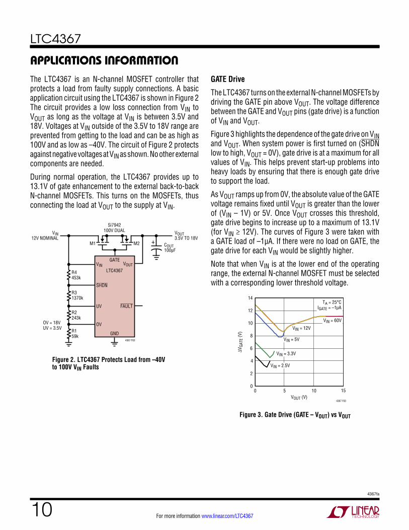
Overvoltage and Undervoltage Protection
The LTC4367 provides two accurate comparators to moni-tor for overvoltage (OV) and undervoltage (UV) conditions at VIN. If the input supply rises above the user adjustable OV threshold, the gate of the external MOSFET is quickly turned off, thus disconnecting the load from the input. Similarly, if the input supply falls below the user adjust-able UV threshold, the gate of the external MOSFET also is quickly turned off. Figure 4 shows a UV/OV application for an input supply of 12V.
The external resistive divider allows the user to select an input supply range that is compatible with the load at VOUT. Furthermore, the UV and OV inputs have very low leakage currents (typically < 1nA at 100°C), allowing for large values in the external resistive divider. In the applica-tion of Figure 4, the load is connected to the supply only if VIN lies between 3.5V and 18V. In the event that VIN goes above 18V or below 3.5V, the gate of the external N-channel MOSFET is immediately discharged with a 60mA current sink, thus isolating the load from the supply.
applicaTions inForMaTion
VIN12V
UV = 3.5V
OV = 18V
4367 F04
DISCHARGE GATEWITH 60mA SINK
LTC4367
OVCOMPARATOR
UVCOMPARATOR
R31820k
UV
0.5V
0.5V
OV
R2243k
R159k –
+25mV
–
+25mV
Figure 4. UV, OV Comparators Monitor 12V Supply
Table 1 lists some external MOSFETs compatible with different VIN supply voltages.
Table 1. Dual MOSFETs for Various Supply RangesVIN MOSFET VTH(MAX) VGS(MAX) VDS(MAX) RDS(ON)
(Ω)
2.5V SiA920 0.7V 5V 8V 0.027
3.3V SiA910 1.0V 8V 12V 0.028
3.3V Si6926 1.0V 8V 20V 0.030
5V SiA906 1.4V 12V 20V 0.046
5V Si9926 1.5V 12V 20V 0.018
>12V SiZ340 2.4V 20V 30V 0.010
>12V Si4288 2.5V 20V 40V 0.020
>12V Si7220 3V 20V 60V 0.060
>12V Si4946 3V 20V 60V 0.040
>12V FDS3890 4V 20V 80V 0.044
>12V Si7942 4V 20V 100V 0.049
>12V FDS3992 4V 20V 100V 0.054
>12V Si7956 4V 20V 150V 0.105

LTC4367
124367fa
For more information www.linear.com/LTC4367
Figure 5 shows the timing associated with the UV pin. Once a UV fault propagates through the UV comparator (tFAULT), the FAULT output is asserted low and a 60mA current sink discharges the GATE pin. As VOUT falls, the GATE pin tracks VOUT.
applicaTions inForMaTion
Figure 6 shows the timing associated with the OV pin. Once an OV fault propagates through the OV comparator (tFAULT), the FAULT output is asserted low and a 60mA current sink discharges the GATE pin. As VOUT falls, the GATE pin tracks VOUT.
Procedure for Selecting UV/OV External Resistor Values
The following 3-step procedure helps select the resistor values for the resistive divider of Figure 4. This procedure minimizes UV and OV offset errors caused by leakage currents at the respective pins.
1. Choose maximum tolerable offset error at the UV pin, VOS(UV). Divide by the worst case leakage current at the UV pin, ILEAK (10nA). Set the sum of R1 + R2 equal to VOS(UV) divided by 10nA. Note that due to the presence of R3, the actual offset at UV will be slightly lower:
R1+ R2 ≤
VOS(UV)
ILEAK
2. Select the desired VIN UV trip threshold, UVTH. Find the value of R3:
R3 =
VOS(UV)
ILEAK•
UVTH – 0.5V
0.5V
3. Select the desired VIN OV trip threshold, OVTH. Find the values of R1 and R2:
R1 =
VOS(UV)
ILEAK
+ R3
OVTH• 0.5V
R2 =
VOS(UV)
ILEAK– R1
The example of Figure 4 uses standard 1% resistor values. The following parameters were selected:
VOS(UV) = 3mV
ILEAK = 10nA
UVTH = 3.5V
OVTH = 18V
4367 F05
FAULT
GATE
tFAULT
tGATE(FAST)
VUV VUV + VUVHYST
tD(ON)
EXTERNAL N-CHANNEL MOSFETSTURN OFF
UV
4367 F06
tFAULT
tGATE(FAST)
VOV VOV – VOVHYST
tD(ON)
EXTERNAL N-CHANNEL MOSFETTURNS OFF
OV
FAULT
GATE
Figure 5. UV Timing (OV < (VOV – VOVHYST), SHDN > 1.2V)
Figure 6. OV Timing (UV > (VUV + VUVHYST), SHDN > 1.2V)
When both the UV and OV faults are removed, the ex-ternal MOSFET is not immediately turned on. The input supply must remain within the user selected power good window for at least 32ms (tD(ON)) before the load is again connected to the supply. This GATE turn-on delay period filters noise (including line noise) at the input supply and prevents chattering of power at the load. For applications that require faster turn-on after a fault, the LTC4367-1 provides a 500µs GATE turn-on delay.

LTC4367
134367fa
For more information www.linear.com/LTC4367
applicaTions inForMaTionThe resistor values can then be solved:
1. R1 + R2 = 3mV
10nA= 300k
2. R3 = 3mV
10nA•
3.5V – 0.5V( )0.5V
= 1.8M
The closest 1% value: R3 = 1.82M:
3. R1 = 300k + 1.82M
2 •18V= 58.9k
The closest 1% value: R1 = 59k:
R2 = 300k – 59k = 241k
The closest 1% value: R2 = 243k
Therefore: OV = 17.93V, UV = 3.51V.
Reverse VIN Protection
The LTC4367’s rugged and hot-swappable VIN input helps protect the more sensitive circuits at the output load. If the input supply is plugged in backwards, or a negative supply is inadvertently connected, the LTC4367 prevents this negative voltage from passing to the output load.
The LTC4367 employs a novel, high speed reverse supply voltage monitor. When the negative VIN voltage is detected, an internal switch connects the gates of the external back-to-back N-channel MOSFETs to the negative input supply.
As shown in Figure 7, external back-to-back N-channel MOSFETs are required for reverse supply protection. When VIN goes negative, the reverse VIN comparator closes the internal switch, which in turn connects the gates of the external MOSFETs to the negative VIN voltage. The body diode (D1) of M1 turns on, but the body diode (D2) of M2 remains in reverse blocking mode. This means that the common source connection of M1 and M2 remains about a diode drop higher than VIN. Since the gate voltage of M2 is shorted to VIN, M2 will be turned off and no cur-rent can flow from VIN to the load at VOUT. Note that the voltage rating of M2 must withstand the reverse voltage excursion at VIN.
Figure 8 illustrates the waveforms that result when VIN is hot plugged to –20V. VIN, GATE and VOUT start out at ground just before the connection is made. Due to the parasitic inductance of the VIN and GATE connections, the voltage at the VIN and GATE pins ring significantly below –20V. Therefore, a 40V N-channel MOSFET was selected to survive the overshoot.
The speed of the LTC4367 reverse protection circuits is evident by how closely the GATE pin follows VIN during the negative transients. The two waveforms are almost indistinguishable on the scale shown.
The trace at VOUT, on the other hand, does not respond to the negative voltage at VIN, demonstrating the desired reverse supply protection. The waveforms of Figure 8 were captured using a 40V dual N-channel MOSFET, a 10µF ceramic output capacitor and no load current on VOUT.
Figure 7. Reverse VIN Protection CircuitsFigure 8. Hot Swapping VIN to –20V
VOUT
VIN
GATE–20V
400ns/DIV
5V/DIV
4367 F08
GND
VIN
4367 F07
VOUTGATE
VIN = –40V
REVERSE VINCOMPARATOR
CLOSES SWITCH WHEN VIN IS NEGATIVEGND
LTC4367
M1
D1 D2
M2
+
–
+
TO LOAD
COUT
LTC4367
144367fa
For more information www.linear.com/LTC4367
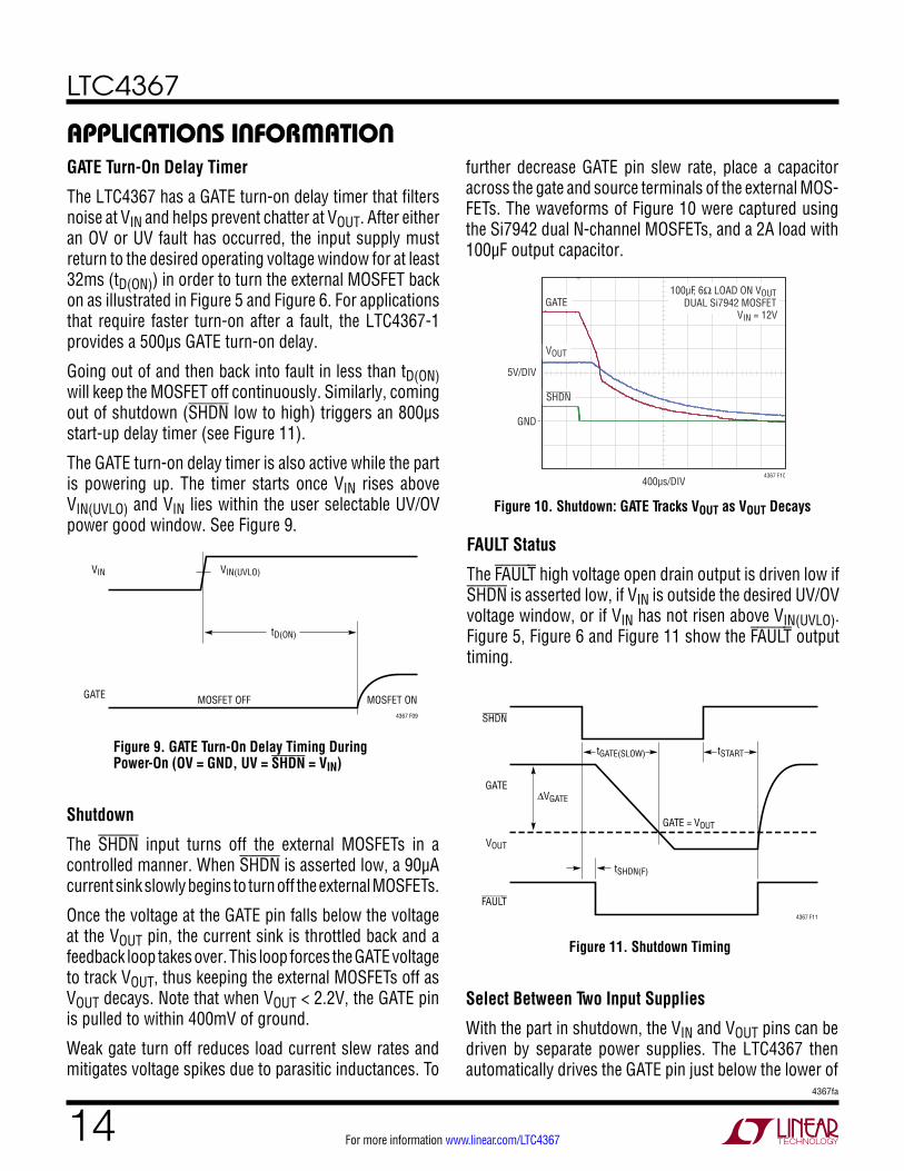
GATE Turn-On Delay Timer
The LTC4367 has a GATE turn-on delay timer that filters noise at VIN and helps prevent chatter at VOUT. After either an OV or UV fault has occurred, the input supply must return to the desired operating voltage window for at least 32ms (tD(ON)) in order to turn the external MOSFET back on as illustrated in Figure 5 and Figure 6. For applications that require faster turn-on after a fault, the LTC4367-1 provides a 500µs GATE turn-on delay.
Going out of and then back into fault in less than tD(ON) will keep the MOSFET off continuously. Similarly, coming out of shutdown (SHDN low to high) triggers an 800µs start-up delay timer (see Figure 11).
The GATE turn-on delay timer is also active while the part is powering up. The timer starts once VIN rises above VIN(UVLO) and VIN lies within the user selectable UV/OV power good window. See Figure 9.
Shutdown
The SHDN input turns off the external MOSFETs in a controlled manner. When SHDN is asserted low, a 90µA current sink slowly begins to turn off the external MOSFETs.
Once the voltage at the GATE pin falls below the voltage at the VOUT pin, the current sink is throttled back and a feedback loop takes over. This loop forces the GATE voltage to track VOUT, thus keeping the external MOSFETs off as VOUT decays. Note that when VOUT < 2.2V, the GATE pin is pulled to within 400mV of ground.
Weak gate turn off reduces load current slew rates and mitigates voltage spikes due to parasitic inductances. To
further decrease GATE pin slew rate, place a capacitor across the gate and source terminals of the external MOS-FETs. The waveforms of Figure 10 were captured using the Si7942 dual N-channel MOSFETs, and a 2A load with 100µF output capacitor.
applicaTions inForMaTion
4367 F09
GATE MOSFET OFF MOSFET ON
VIN VIN(UVLO)
tD(ON)
Figure 9. GATE Turn-On Delay Timing During Power-On (OV = GND, UV = SHDN = VIN)
Figure 10. Shutdown: GATE Tracks VOUT as VOUT Decays
GATE
VOUT
tGATE(SLOW)
GATE = VOUT
tSTART
tSHDN(F)
∆VGATE
SHDN
4367 F11
FAULT
Figure 11. Shutdown Timing
FAULT Status
The FAULT high voltage open drain output is driven low if SHDN is asserted low, if VIN is outside the desired UV/OV voltage window, or if VIN has not risen above VIN(UVLO). Figure 5, Figure 6 and Figure 11 show the FAULT output timing.
SHDN
GATE
VOUT
100µF, 6Ω LOAD ON VOUTDUAL Si7942 MOSFET
VIN = 12V
400µs/DIV
5V/DIV
4367 F10
GND
Select Between Two Input Supplies
With the part in shutdown, the VIN and VOUT pins can be driven by separate power supplies. The LTC4367 then automatically drives the GATE pin just below the lower of

LTC4367
154367fa
For more information www.linear.com/LTC4367
the two supplies, thus turning off the external back-to-back MOSFETs. The application of Figure 12 uses two LTC4367s to select between two power supplies. Care should be taken to ensure that only one of the two LTC4367s is enabled at any given time.
applicaTions inForMaTion
Figure 12. Selecting One of Two Supplies
VIN
V2
SHDN
4367 F12
VOUTGATE
LTC4367
VIN
V1
SEL01
OUTV1V2
OUT
M2M1
M2M1
SEL
SHDN
VOUTGATE
LTC4367
Limiting Inrush Current During Turn-On
The LTC4367 turns on the external N-channel MOSFET with a 35µA current source. The maximum slew rate at the GATE pin can be reduced by adding a capacitor on the GATE pin:
Slew Rate = 35µA
CGATE
Since the MOSFET acts like a source follower, the slew rate at VOUT equals the slew rate at GATE.
Therefore, inrush current is given by:
IINRUSH = COUT
CGATE• 35µA
For example, a 1A inrush current to a 330µF output capacitance requires a GATE capacitance of:
CGATE = 35µA •COUT
IINRUSH
CGATE = 35µA • 330µF
1A= 11.6nF
The 12nF CGATE capacitor in the application circuit of Figure 14 limits the inrush current to just under 1A. RGATE makes sure that CGATE does not affect the fast GATE turn off characteristics during UV/OV faults, or during reverse VIN connection. R5A and R5B help prevent high frequency oscillations with the external N-channel MOSFET and related board parasitics.
Figure 13. Single MOSFET Application Protects Against 100V Figure 14. Limiting Inrush Current with CGATE
Single MOSFET Application
When reverse VIN protection is not needed, a single external N-channel MOSFET may be used. The application circuit of Figure 13 connects the load to VIN when VIN is less than 30V, and uses the minimal set of external components.
VIN
UV
OV
SHDN
OV = 30V
4367 F13
VOUT
FAULT
GATE
VIN24V
SiR870100V
VOUT
GND
LTC4367
R21870k
R140.2k
COUT100µF
+
R4499k
4367 F14
VIN
VIN VOUT
R5B10Ω
R5A10Ω
COUT330µF
VOUTGATE
LTC4367
RGATE5.1k
CGATE12nF
+
M2M1

LTC4367
164367fa
For more information www.linear.com/LTC4367
applicaTions inForMaTionTransients During OV Fault
The circuit of Figure 15 is used to display transients dur-ing an overvoltage condition. The nominal input supply is 48V and it has an overvoltage threshold of 60V. The parasitic inductance is that of a 1 foot wire (roughly 300nH). Figure 16 shows the waveforms during an overvoltage condition at VIN. These transients depend on the parasitic inductance and resistance of the wire along with the ca-
pacitance at the VIN node. D1 is an optional power clamp (TVS, TransZorb) recommended for applications where VIN can ring above 100V. No clamp was used to capture the waveforms of Figure 16. In order to maintain reverse supply protection, D1 must be a bidirectional clamp rated for at least 225W peak pulse power dissipation.
400ns/DIV
VIN20V/DIV
VOUT20V/DIV
GATE
IIN2A/DIV
4367 F16
60V
60V
0A
Figure 15. OV Fault with Large VIN Inductance
Figure 16. Transients During OV Fault When No TransZorb (TVS) Is Used
VIN
UV
OV
SHDN
OV = 60V
4367 F15
VOUT
FAULT
GATE
M1 M2
VIN48V
Si7942100V DUAL
12 INCH WIRELENGTH VOUT
GND
LTC4367
R22430k
R120.5k
R4523k
COUT100µF
+CIN1000µF
D1OPTIONAL
+22Ω
LTC4367
174367fa
For more information www.linear.com/LTC4367
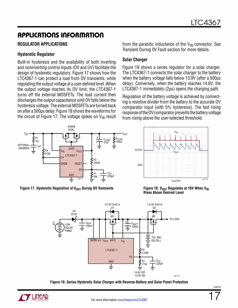
REGULATOR APPLICATIONS
Hysteretic Regulator
Built-in hysteresis and the availability of both inverting and noninverting control inputs (OV and UV) facilitate the design of hysteretic regulators. Figure 17 shows how the LTC4367-1 can protect a load from OV transients, while regulating the output voltage at a user-defined level. When the output voltage reaches its OV limit, the LTC4367-1 turns off the external MOSFETs. The load current then discharges the output capacitance until OV falls below the hysteresis voltage. The external MOSFETs are turned back on after a 500µs delay. Figure 18 shows the waveforms for the circuit of Figure 17. The voltage spikes on VIN result
from the parasitic inductance of the VIN connector. See Transient During 0V Fault section for more details.
Solar Charger
Figure 19 shows a series regulator for a solar charger. The LTC4367-1 connects the solar charger to the battery when the battery voltage falls below 13.9V (after a 500µs delay). Conversely, when the battery reaches 14.6V, the LTC4367-1 immediately (2µs) opens the charging path.
Regulation of the battery voltage is achieved by connect-ing a resistive divider from the battery to the accurate OV comparator input (with 5% hysteresis). The fast rising response of the OV comparator prevents the battery voltage from rising above the user-selected threshold.
applicaTions inForMaTion
Figure 17. Hysteretic Regulation of VOUT During OV Transients Figure 18. VOUT Regulates at 16V When VIN Rises Above Desired Level
GND
VIN
VOUT
1ms/DIV
5V/DIV
4367 F18
VIN
4367 F19
VOUT GATEUVSHDN
1/2 OF Si4214 1/2 OF Si4214
GND
LTC4367-1
OV
M1
D1D4
B130
D2
M2
+TO LOAD
CBATT100µF
CBYP100nF15W
SOLARPANEL
R23.24M
R1115k
14.6V OFF13.9V ON
COV220pF
12V, 8AhGELCELL
Figure 19. Series Hysteretic Solar Charger with Reverse-Battery and Solar Panel Protection
VIN
UV
OV
SHDN
4367 F17
VOUT
FAULT
GATE
VIN
Si4946DUAL
OPTIONALSNUBBER
VOUT
GND
LTC4367-1
R4510k
CLOAD47µF
COV220pF
+ RLOAD100Ω
R21820k
R159k
1µF
R71Ω

LTC4367
184367fa
For more information www.linear.com/LTC4367
applicaTions inForMaTionNote that during initial start-up, the LTC4367-1 will not turn on the external MOSFETs until a battery is first con-nected to the VIN pin. To begin operation, VIN must initially rise above the 2.2V UVLO lockout voltage. Connecting the battery ensures that the LTC4367-1 comes out of UVLO.
12V Application with 150V Transient Protection
Figure 20 shows a 12V application that withstands input supply transients up to 150V. When the input voltage ex-ceeds 17.9V, the OV resistive divider turns off the external MOSFETs. As VIN rises to 150V, the gate of transistor M1 remains in the Off condition, thus preventing conduction from VIN to VOUT. Note that M1 must have an operating range above 150V.
Resistor R6 and diode D3 clamp the LTC4367 supply volt-age to 50V. To prevent R6 from interfering with reverse operation, the recommended value is 1k or less. Note that the power handling capability of R6 must be considered in order to avoid overheating during transients. D3 is shown as a bidirectional clamp in order to achieve reverse-polarity protection at VIN. M2 is also required in order to protect VOUT from negative voltages at VIN and should have an operating range beyond the breakdown of D3. If reverse protection is not desired remove M2 and connect the source of M1 directly to VOUT.
MOSFET Selection
To protect against a negative voltage at VIN, the external N-channel MOSFETs must be configured in a back-to-back arrangement. Dual N-channel packages are thus the best choice. The MOSFET is selected based on its power
handling capability, drain and gate breakdown voltages, and threshold voltage.
The drain to source breakdown voltage must be higher than the maximum voltage expected between VIN and VOUT. Note that if an application generates high energy transients during normal operation or during hot swap, the external MOSFET must be able to withstand this transient voltage.
Due to the high impedance nature of the charge pump that drives the GATE pin, the total leakage on the GATE pin must be kept low. The gate drive curves of Figure 3 were measured with a 1µA load on the GATE pin. Therefore, the leakage on the GATE pin must be no greater than 1µA in order to match the curves of Figure 3. Higher leakage currents will result in lower gate drive. The dual N-channel MOSFETs shown in Table 1 all have a maximum gate leakage current of 100nA. Additionally, Table 1 lists representative MOSFETs that would work at different values of VIN.
Layout Considerations
The trace length between the VIN pin and the drain of the external MOSFET should be minimized, as well as the trace length between the GATE pin of the LTC4367 and the gates of the external MOSFETs.
Place the bypass capacitors at VOUT as close as possible to the external MOSFET. Use high frequency ceramic capacitors in addition to bulk capacitors to mitigate hot swap ringing. Place the high frequency capacitors closest to the MOSFET. Note that bulk capacitors mitigate ringing by virtue of their ESR. Ceramic capacitors have low ESR and can thus ring near their resonant frequency.
Figure 20. 12V Application Protected from 150V Transients
VIN
UV
OV
SHDN
D3: SMAJ43CA BI-DIRECTIONAL
OV = 17.9V
4367 F20
VOUT
FAULT
GATE
VIN12V
M1FDD2572
M2FDS5680
VOUT
GND
LTC4367R4510k
D3R22050k
R159k
R61k

LTC4367
194367fa
For more information www.linear.com/LTC4367
package DescripTionPlease refer to http://www.linear.com/product/LTC4367#packaging for the most recent package drawings.
MSOP (MS8) 0213 REV G
0.53 ±0.152(.021 ±.006)
SEATINGPLANE
NOTE:1. DIMENSIONS IN MILLIMETER/(INCH)2. DRAWING NOT TO SCALE3. DIMENSION DOES NOT INCLUDE MOLD FLASH, PROTRUSIONS OR GATE BURRS. MOLD FLASH, PROTRUSIONS OR GATE BURRS SHALL NOT EXCEED 0.152mm (.006") PER SIDE4. DIMENSION DOES NOT INCLUDE INTERLEAD FLASH OR PROTRUSIONS. INTERLEAD FLASH OR PROTRUSIONS SHALL NOT EXCEED 0.152mm (.006") PER SIDE5. LEAD COPLANARITY (BOTTOM OF LEADS AFTER FORMING) SHALL BE 0.102mm (.004") MAX
0.18(.007)
0.254(.010)
1.10(.043)MAX
0.22 – 0.38(.009 – .015)
TYP
0.1016 ±0.0508(.004 ±.002)
0.86(.034)REF
0.65(.0256)
BSC
0° – 6° TYP
DETAIL “A”
DETAIL “A”
GAUGE PLANE
1 2 3 4
4.90 ±0.152(.193 ±.006)
8 7 6 5
3.00 ±0.102(.118 ±.004)
(NOTE 3)
3.00 ±0.102(.118 ±.004)
(NOTE 4)
0.52(.0205)
REF
5.10(.201)MIN
3.20 – 3.45(.126 – .136)
0.889 ±0.127(.035 ±.005)
RECOMMENDED SOLDER PAD LAYOUT
0.42 ± 0.038(.0165 ±.0015)
TYP
0.65(.0256)
BSC
MS8 Package8-Lead Plastic MSOP
(Reference LTC DWG # 05-08-1660 Rev G)

LTC4367
204367fa
For more information www.linear.com/LTC4367
package DescripTionPlease refer to http://www.linear.com/product/LTC4367#packaging for the most recent package drawings.
3.00 ±0.10(4 SIDES)
NOTE:1. DRAWING TO BE MADE A JEDEC PACKAGE OUTLINE M0-229 VARIATION OF (WEED-1)2. DRAWING NOT TO SCALE3. ALL DIMENSIONS ARE IN MILLIMETERS4. DIMENSIONS OF EXPOSED PAD ON BOTTOM OF PACKAGE DO NOT INCLUDE MOLD FLASH. MOLD FLASH, IF PRESENT, SHALL NOT EXCEED 0.15mm ON ANY SIDE5. EXPOSED PAD SHALL BE SOLDER PLATED6. SHADED AREA IS ONLY A REFERENCE FOR PIN 1 LOCATION ON TOP AND BOTTOM OF PACKAGE
0.40 ±0.10
BOTTOM VIEW—EXPOSED PAD
1.65 ±0.10(2 SIDES)
0.75 ±0.05
R = 0.125TYP
2.38 ±0.10
14
85
PIN 1TOP MARK
(NOTE 6)
0.200 REF
0.00 – 0.05
(DD8) DFN 0509 REV C
0.25 ±0.05
2.38 ±0.05
RECOMMENDED SOLDER PAD PITCH AND DIMENSIONSAPPLY SOLDER MASK TO AREAS THAT ARE NOT SOLDERED
1.65 ±0.05(2 SIDES)2.10 ±0.05
0.50BSC
0.70 ±0.05
3.5 ±0.05
PACKAGEOUTLINE
0.25 ±0.050.50 BSC
DD Package8-Lead Plastic DFN (3mm × 3mm)
(Reference LTC DWG # 05-08-1698 Rev C)
LTC4367
214367fa
For more information www.linear.com/LTC4367Information furnished by Linear Technology Corporation is believed to be accurate and reliable. However, no responsibility is assumed for its use. Linear Technology Corporation makes no representa-tion that the interconnection of its circuits as described herein will not infringe on existing patent rights.
revision hisToryREV DATE DESCRIPTION PAGE NUMBER
A 03/16 Updated Typical Application and Figures 1, 2, 13, 15Updated SHDN, UV input current ratingChanged ISHDN test condition to 10V from 0.75VUpdated graphs G09 and G12Updated SHDN and UV Pin Functions
1, 9, 10, 15, 1624
5, 67

LTC4367
224367fa
For more information www.linear.com/LTC4367 LINEAR TECHNOLOGY CORPORATION 2015
LT 0316 REV A • PRINTED IN USALinear Technology Corporation1630 McCarthy Blvd., Milpitas, CA 95035-7417(408) 432-1900 FAX: (408) 434-0507 www.linear.com/LTC4367
relaTeD parTs
Typical applicaTionLTC4367 Protects Step Down Regulator from –30V to 30V VIN Faults
PART NUMBER DESCRIPTION COMMENTS
LTC4365 Overvoltage, Undervoltage and Reverse Supply Protection Controller
Wide Operating Range: 2.5V to 34V, Protection Range: –40V to 60V, No TVS Required for Most Applications
LT4363 Surge Stopper Overvoltage/Overcurrent Protection Regulator
Wide Operating Range: 4V to 80V, Reverse Protection to –60V, Adjustable Output Clamp Voltage
LTC4364 Surge Stopper with Ideal Diode 4V to 80V Operation, –40V Reverse Input, –20V Reverse Output
LTC4366 Floating Surge Stopper 9V to >500V Operation, 8-Pin TSOT and 3mm × 2mm DFN Packages
LTC4361 Overvoltage/Overcurrent Protection Controllers 5.8V Overvoltage Threshold, 85V Absolute Maximum
LTC2909 Triple/Dual Inputs UV/OV Negative Monitor Pin Selectable Input Polarity Allows Negative and OV Monitoring
LTC2912/LTC2913 Single/Dual UV/OV Voltage Monitor Adjustable UV and OV Trip Values, ±1.5% Threshold Accuracy
LTC2914 Quad UV/OV Monitor For Positive and Negative Supplies
LTC2955 Pushbutton On/Off Controller Automatic Turn-On, 1.5V to 36V Input, ±36V PB Input
LT4256 Positive 48V Hot Swap Controller with Open-Circuit Detect
Foldback Current Limiting, Open-Circuit and Overcurrent Fault Output, Up to 80V Supply
LTC4260 Positive High Voltage Hot Swap Controller with ADC and I2C
Wide Operating Range 8.5V to 80V
LTC4352 Ideal MOSFET ORing Diode External N-Channel MOSFETs Replace ORing Diodes, 0V to 18V
LTC4354 Negative Voltage Diode-OR Controller Controls Two N-Channel MOSFETs, 1.2µs Turn-Off, –80V Operation
LTC4355 Positive Voltage Diode-OR Controller Controls Two N-Channel MOSFETs, 0.4µs Turn-Off, 80V Operation
LT1913 Step-Down Switching Regulator 3.6V to 25V Input, 3.5A Maximum Current, 200kHz to 2.4MHz
VIN
UV
OV
SHDN
OV = 18VUV = 3.5V
4367 TA02
VOUT
FAULT
GATE
Si4214 30VDUAL N-CHANNEL
VOUT PROTECTEDFROM –30V TO 30V
VIN12V NOMINAL
VOUT
GND
LTC4367510k
10µF
1820k
243k
59k
SW
FB
VC
PG
RT
VIN BD
OUTPUT5V3.5A
0.47µF
47µF100k
15k
63.4k
4.7µH
536k
GND
LT1913
RUN/SS BOOST
SYNC
680pF