LT3995 - 60V, 3A, 2MHz Step-Down Switching Regulator with ... · 60V, 3A, 2MHz Step-Down Switching...
24
LT3995 1 3995f For more information www.linear.com/LT3995 TYPICAL APPLICATION FEATURES DESCRIPTION 60V, 3A, 2MHz Step-Down Switching Regulator with 2.7µA Quiescent Current The LT ® 3995 is an adjustable frequency monolithic buck switching regulator that accepts a wide input voltage range up to 60V. Low quiescent current design consumes only 2.7µA of supply current while regulating with no load. Low ripple Burst Mode operation maintains high efficiency at low output currents while keeping the output ripple below 15mV in a typical application. The LT3995 can supply up to 3A of load current and has current limit foldback to limit power dissipation during short circuit. A low dropout voltage of 500mV is maintained when the input voltage drops below the programmed output voltage, such as during automotive cold crank. An internally compensated current mode topology is used for fast transient response and good loop stability. A high efficiency 85mΩ switch is included on the die along with a boost Schottky diode and the necessary oscillator, control, and logic circuitry. An accurate 1.02V threshold enable pin can be driven directly from a microcontroller or used as a programmable undervoltage lockout. A capacitor on the SS pin provides a controlled inrush current (soft-start). A power good flag signals when V OUT reaches 91.6% of the programmed output voltage. The LT3995 is available in a small 16-lead MSOP package with exposed pad for low thermal resistance. No-Load Supply Current 3.3V Step-Down Converter APPLICATIONS n Ultralow Quiescent Current: 2.7µA I Q at 12V IN to 3.3V OUT n Low Ripple Burst Mode ® Operation Output Ripple < 15mV P-P n Wide Input Range: Operation from 4.3V to 60V n 3A Maximum Output Current n Excellent Start-Up and Dropout Performance n Adjustable Switching Frequency: 200kHz to 2MHz n Synchronizable Between 250kHz to 2MHz n Accurate Programmable Undervoltage Lockout n Low Shutdown Current: I Q = 700nA n Power Good Flag n Soft-Start Capability n Thermal Shutdown Protection n Current Limit Foldback with SS Override n Saturating Switch Design: 85mΩ On Resistance n Small, Thermally Enhanced 16-Lead MSOP Package n Automotive Battery Regulation n Portable Products n Industrial Supplies L, LT, LTC, LTM, Burst Mode, Linear Technology and the Linear logo are registered trademarks of Linear Technology Corporation. All other trademarks are the property of their respective owners. V IN EN BOOST OFF ON V IN 4.3V TO 60V PG 0.47μF 47μF 1210 ×2 PDS560 3995 TA01a 10nF 10μF 576k 182k f = 300kHz V OUT 3.3V 3A 8.2μH LT3995 SS RT SW OUT FB SYNC GND 1M 10pF INPUT VOLTAGE (V) 0 1.0 INPUT CURRENT (μA) 1.5 2.5 3.0 3.5 30 35 40 50 45 55 4.5 3995 TA01b 2.0 5 10 15 20 25 60 4.0 IN REGULATION
Transcript of LT3995 - 60V, 3A, 2MHz Step-Down Switching Regulator with ... · 60V, 3A, 2MHz Step-Down Switching...
LT3995
13995f
For more information www.linear.com/LT3995
TYPICAL APPLICATION
FEATURES DESCRIPTION
60V, 3A, 2MHz Step-Down Switching Regulator with 2.7µA Quiescent Current
The LT®3995 is an adjustable frequency monolithic buck switching regulator that accepts a wide input voltage range up to 60V. Low quiescent current design consumes only 2.7µA of supply current while regulating with no load. Low ripple Burst Mode operation maintains high efficiency at low output currents while keeping the output ripple below 15mV in a typical application. The LT3995 can supply up to 3A of load current and has current limit foldback to limit power dissipation during short circuit. A low dropout voltage of 500mV is maintained when the input voltage drops below the programmed output voltage, such as during automotive cold crank.
An internally compensated current mode topology is used for fast transient response and good loop stability. A high efficiency 85mΩ switch is included on the die along with a boost Schottky diode and the necessary oscillator, control, and logic circuitry. An accurate 1.02V threshold enable pin can be driven directly from a microcontroller or used as a programmable undervoltage lockout. A capacitor on the SS pin provides a controlled inrush current (soft-start). A power good flag signals when VOUT reaches 91.6% of the programmed output voltage. The LT3995 is available in a small 16-lead MSOP package with exposed pad for low thermal resistance.
No-Load Supply Current3.3V Step-Down Converter
APPLICATIONS
n Ultralow Quiescent Current: 2.7µA IQ at 12VIN to 3.3VOUTn Low Ripple Burst Mode® Operation Output Ripple < 15mVP-Pn Wide Input Range: Operation from 4.3V to 60Vn 3A Maximum Output Currentn Excellent Start-Up and Dropout Performancen Adjustable Switching Frequency: 200kHz to 2MHzn Synchronizable Between 250kHz to 2MHzn Accurate Programmable Undervoltage Lockoutn Low Shutdown Current: IQ = 700nAn Power Good Flagn Soft-Start Capabilityn Thermal Shutdown Protectionn Current Limit Foldback with SS Overriden Saturating Switch Design: 85mΩ On Resistancen Small, Thermally Enhanced 16-Lead MSOP Package
n Automotive Battery Regulationn Portable Productsn Industrial SuppliesL, LT, LTC, LTM, Burst Mode, Linear Technology and the Linear logo are registered trademarks of Linear Technology Corporation. All other trademarks are the property of their respective owners.
VIN
EN BOOSTOFF ON
VIN4.3V TO 60V
PG0.47µF
47µF1210×2
PDS560
3995 TA01a
10nF
10µF
576k182k
f = 300kHz
VOUT3.3V3A
8.2µH
LT3995
SS
RT
SW
OUT
FBSYNC GND
1M
10pF
INPUT VOLTAGE (V)0
1.0
INPU
T CU
RREN
T (µ
A)
1.5
2.5
3.0
3.5
30 35 40 5045 55
4.5
3995 TA01b
2.0
5 10 15 20 25 60
4.0
IN REGULATION
LT3995
23995f
For more information www.linear.com/LT3995
The l denotes the specifications which apply over the full operating temperature range, otherwise specifications are at TA = 25°C. (Note 2)
ABSOLUTE MAXIMUM RATINGS
VIN, EN Voltage (Note 3) ...........................................60VBOOST Pin Voltage ...................................................75VBOOST Pin Above SW Pin .........................................30VFB, RT, SYNC, SS Voltage ...........................................6V PG Voltage ................................................................30VOUT Voltage ..............................................................16VOperating Junction Temperature Range (Note 2) LT3995E ............................................ –40°C to 125°C LT3995I ............................................. –40°C to 125°C LT3995H ............................................ –40°C to 150°CStorage Temperature Range .................. –65°C to 150°CLead Temperature (Soldering, 10 sec) ................... 300°C
(Note 1)
12345678
FBSS
OUTBOOST
SWSWSWNC
161514131211109
SYNCPGRTENVINVINVINNC
TOP VIEW
17GND
MSE PACKAGE16-LEAD PLASTIC MSOP
θJA = 40°C/W EXPOSED PAD (PIN 17) IS GND, MUST BE SOLDERED TO PCB
PIN CONFIGURATION
ELECTRICAL CHARACTERISTICS
ORDER INFORMATIONLEAD FREE FINISH TAPE AND REEL PART MARKING* PACKAGE DESCRIPTION TEMPERATURE RANGE
LT3995EMSE#PBF LT3995EMSE#TRPBF 3995 16-Lead Plastic MSOP –40°C to 125°C
LT3995IMSE#PBF LT3995IMSE#TRPBF 3995 16-Lead Plastic MSOP –40°C to 125°C
LT3995HMSE#PBF LT3995HMSE#TRPBF 3995 16-Lead Plastic MSOP –40°C to 150°C
Consult LTC Marketing for parts specified with wider operating temperature ranges. *The temperature grade is identified by a label on the shipping container.Consult LTC Marketing for information on non-standard lead based finish parts.For more information on lead free part marking, go to: http://www.linear.com/leadfree/ For more information on tape and reel specifications, go to: http://www.linear.com/tapeandreel/
PARAMETER CONDITIONS MIN TYP MAX UNITSMinimum Input Voltage (Note 3) l 4 4.3 VDropout Comparator Threshold (VIN – OUT) Falling 430 500 570 mVDropout Comparator Threshold Hysteresis 25 mVQuiescent Current from VIN VEN Low
VEN High, VSYNC Low VEN High, VSYNC Low
l
0.7 1.6
1.3 2.7 30
µA µA µA
FB Pin Current VFB = 1.5V l 0.1 12 nAFeedback Voltage
l
1.183 1.173
1.197 1.197
1.212 1.222
V V
FB Voltage Line Regulation 4.3V < VIN < 60V (Note 3) 0.0003 0.01 %/VSwitching Frequency RT = 11.8k
RT = 41.2k RT = 294k
1.8 0.8 160
2.25 1
200
2.7 1.2 240
MHz MHz kHz
Minimum Switch On-Time 130 nsMinimum Switch Off-Time (Note 4) 180 280 ns
LT3995
33995f
For more information www.linear.com/LT3995
ELECTRICAL CHARACTERISTICS The l denotes the specifications which apply over the full operating temperature range, otherwise specifications are at TA = 25°C. (Note 2)
Note 1: Stresses beyond those listed under Absolute Maximum Ratings may cause permanent damage to the device. Exposure to any Absolute Maximum Rating condition for extended periods may affect device reliability and lifetime.Note 2: The LT3995E is guaranteed to meet performance specifications from 0°C to 125°C junction temperature. Specifications over the –40°C to 125°C operating junction temperature range are assured by design, characterization, and correlation with statistical process controls. The LT3995I is guaranteed over the full –40°C to 125°C operating junction temperature range. The LT3995H is guaranteed over the full –40°C to 150°C operating junction temperature range. High junction temperatures degrade operating lifetimes. Operating lifetime is derated at junction temperatures greater than 125°C. The junction temperature (TJ, in °C) is calculated from the ambient temperature (TA, in °C) and power dissipation (PD, in Watts) according to the formula: TJ = TA + (PD • θJA) where θJA (in °C/W) is the package thermal impedance.
Note 3: Minimum input voltage depends on application circuit.Note 4: The LT3995 contains circuitry that extends the maximum duty cycle if there is sufficient voltage across the boost capacitor. See the Application Information section for more details.Note 5: This is the minimum voltage across the boost capacitor needed to guarantee full saturation of the switch.Note 6: This IC includes overtemperature protection that is intended to protect the device during momentary overload conditions. Junction temperature will exceed the maximum operating junction temperature when overtemperature protection is active. Continuous operation above the specified maximum operating junction temperature may impair device reliability or permanently damage the device.
Switch Current Limit VFB = 1V 4.7 6.3 7.9 AFoldback Switch Current Limit VFB = 0V 3.1 ASwitch VCESAT ISW = 1A 100 mVSwitch Leakage Current 0.02 1 μABoost Schottky Forward Voltage ISH = 100mA 800 mVBoost Schottky Reverse Leakage VREVERSE = 12V 0.02 2 μAMinimum Boost Voltage (Note 5) l 1.3 1.8 VBOOST Pin Current ISW = 1A, VBOOST – VSW = 3V 22 35 mAEN Voltage Threshold EN Falling, VIN ≥ 4.3V l 0.92 1.02 1.12 VEN Voltage Hysteresis 60 mVEN Pin Current 0.2 20 nAPG Threshold Offset from VFB VFB Falling 5 8.4 13 %PG Hysteresis as % of Output Voltage 1.7 %PG Leakage VPG = 3V 0.02 1 µAPG Sink Current VPG = 0.4V l 125 480 μASYNC Low Threshold 0.6 1.0 VSYNC High Threshold 1.18 1.5 VSYNC Pin Current VSYNC = 6V 0.1 nASS Source Current VSS = 0.5V 0.9 1.8 2.6 μA

LT3995
43995f
For more information www.linear.com/LT3995
TYPICAL PERFORMANCE CHARACTERISTICS
Efficiency at 3.3VOUT No-Load Supply Current No-Load Supply Current
Reference Voltage
Efficiency at 5VOUT Efficiency at 3.3VOUT Efficiency at 5VOUT
Load Regulation Line Regulation
TA = 25°C, unless otherwise noted.
LOAD CURRENT (A)0
50
EFFI
CIEN
CY (%
)
60
70
80
0.5 1 1.5 2
3995 G01
2.5
90
100
55
65
75
85
95
3
12V24V36V48V
L: MSS1260-682MLfSW = 500kHz
LOAD CURRENT (A)0
40
EFFI
CIEN
CY (%
)
50
60
70
0.5 1 1.5 2
3995 G02
2.5
80
90
45
55
65
75
85
3
12V24V36V48V
L: MSS1260-822MLfSW = 300kHz
LOAD CURRENT (mA)0.01
0
EFFI
CIEN
CY (%
)
20
40
60
0.1 1 10 100
3995 G03
1000
80
100
10
30
50
70
90
10000
12V24V36V48V
L: MSS1260-682MLfSW = 500kHz
LOAD CURRENT (mA)0.01
0
EFFI
CIEN
CY (%
)
20
40
60
0.1 1 10 100
3995 G04
1000
80
100
10
30
50
70
90
10000
12V24V36V48V
L: MSS1260-822MLfSW = 300kHz
INPUT VOLTAGE (V)0
1.0
INPU
T CU
RREN
T (µ
A)
1.5
2.5
3.0
3.5
30 35 40 5045 55
4.5
3995 G05
2.0
5 10 15 20 25 60
4.0
IN REGULATIONVOUT = 3.3V
TEMPERATURE (°C)
10
INPU
T CU
RREN
T (µ
A)
1000
10000
–55 65 125
3975 G06
15–25 95 15535
100
FRONT PAGE APPLICATIONVIN = 12VVOUT = 3.3V
DUE TO CATCHDIODE LEAKAGE
TEMPERATURE (°C)–55
REFE
RENC
E VO
LTAG
E (V
)
1.190
1.220
1.225
1.230
5 65 95
3995 G07
1.180
1.175
1.210
1.200
1.185
1.215
1.170
1.205
1.195
–25 35 125 155LOAD CURRENT (A)
0
CHAN
GE IN
VOU
T (%
)
0
3995 G08
–0.10
–0.201 20.5 1.5 2.5
0.10
0.20
–0.05
–0.15
0.05
0.15
3
VIN = 12VVOUT = 5V
INPUT VOLAGE (V)
–0.15
CHAN
GE IN
VOU
T (%
)
–0.05
0.05
0.15
–0.10
0
0.10
15 3025 40 50
3995 G09
60105 20 35 45 55
VOUT = 5VLOAD = 1A

LT3995
53995f
For more information www.linear.com/LT3995
TYPICAL PERFORMANCE CHARACTERISTICS
Switch Current Limit
Switch Current Limit Current Limit Foldback Soft-Start
Switch VCESAT BOOST Pin Current
Thermal Derating Thermal Derating
TA = 25°C, unless otherwise noted.
Minimum On-Time
DUTY CYCLE0
4.0
CURR
ENT
LIM
IT (A
)
4.5
5.0
5.5
6.0
6.5
7.0
0.2 0.4 0.6 0.8
3995 G11
1.0
TEMPERATURE (°C)–55
CURR
ENT
LIM
IT (A
)
6.0
6.5
7.0
35 95
3995 G12
5.5
5.0
–25 5 65 125 155
4.5
4.0
30% DUTY CYCLE
FB PIN VOLTAGE (V)0
7
6
5
4
3
2
1
00.6 1.0
3995 G13
0.2 0.4 0.8 1.2
CURR
ENT
LIM
IT (A
)
30% DUTY CYCLEVSS = 3V
SS PIN VOLTAGE (V)0
5
6
7
2
3995 G14
4
3
0.5 1 1.5 2.5
2
1
0
CURR
ENT
LIM
IT (A
)
VFB = 1V30% DUTY CYCLE
VFB = 0.2V
SWITCH CURRENT (A)0
0
SWIT
CH D
ROP
(mV)
50
100
150
200
300
0.5 1 1.5 2
3995 G15
2.5 3
250
SWITCH CURRENT (A)0
70
60
50
40
30
20
10
01.5 2.5
3995 G16
0.5 1 2 3
BOOS
T PI
N CU
RREN
T (m
A)
TEMPERATURE (°C)–55
MIN
IMUM
ON-
TIM
E (n
s)
175
200
225
35 95
3995 G17
150
125
–25 5 65 125 155
100
75
LOAD = 2A
LOAD = 1A
VSYNC = 0VfSW = 2MHz
TEMPERATURE (°C)0
3.5
3.0
2.5
2.0
1.5
1.0
0.5
075 125
3995 G10
25 50 100 150
LOAD
CUR
RENT
(A)
VOUT = 3.3VfSW = 300kHz2.5in × 2.5in 4-LAYER BOARD
LIMITED BY MAXIMUM JUNCTIONTEMPERATURE θJA = 40°C/W
12VIN24VIN36VIN48VIN60VIN
H-GRADE
TEMPERATURE (°C)0
3.5
3.0
2.5
2.0
1.5
1.0
0.5
075 125
3995 G38
25 50 100 150
LOAD
CUR
RENT
(A)
VOUT = 5VfSW = 500kHz2.5in × 2.5in 4-LAYER BOARD
LIMITED BY MAXIMUM JUNCTIONTEMPERATURE θJA = 40°C/W
12VIN24VIN36VIN48VIN60VIN
H-GRADE

LT3995
63995f
For more information www.linear.com/LT3995
TYPICAL PERFORMANCE CHARACTERISTICS
Switching FrequencyRT Programmed Switching Frequency
Frequency FoldbackInternal Undervoltage Lockout (UVLO) EN Threshold
PG ThresholdsMinimum Input Voltage, VOUT = 5V
Minimum Input Voltage, VOUT = 3.3V
TA = 25°C, unless otherwise noted.
TEMPERATURE (°C)–55
SWIT
CHIN
G FR
EQUE
NCY
(kHz
)
660
720
780
35 95
3995 G19
600
540
–25 5 65 125 155
480
420
RT = 78.7k
SWITCHING FREQUENCY (MHz)0.2
0
R T R
ESIS
TOR
(kΩ
)
50
150
200
250
350
0.4 1.2 1.6
3995 G20
100
300
1.0 2.0 2.20.6 0.8 1.4 1.8
FB PIN VOLTAGE (V)0
700
600
500
400
300
200
100
00.6 1
3995 G21
0.2 0.4 0.8 1.2
SWIT
CHIN
G FR
EQUE
NCY
(kHz
)
RT = 78.7k
TEMPERATURE (°C)–55
INPU
T VO
LTAG
E (V
)
4
5
6
35 95
3995 G22
3
2
–25 5 65 125 155
1
0
TEMPERATURE (°C)–55
EN T
HRES
HOLD
(V)
1.08
35
3995 G23
1.05
1.03
–25 5 65
1.02
1.01
1.09
1.07
1.06
1.04
95 125 155
EN RISING
EN FALLING
TEMPERATURE (°C)–55
PG T
HRES
HOLD
(V)
1.11
35
3995 G24
1.08
1.06
–25 5 65
1.05
1.04
1.12
1.10
1.09
1.07
95 125 155
FB RISING
FB FALLING
LOAD CURRENT (A)0
4.0
INPU
T VO
LTAG
E (V
)
4.5
5.0
5.5
6.0
6.5
0.5 1.0 1.5 2.0
3995 G25
2.5 3.0
VOUT = 5VfSW = 500kHz
TO RUN/TO START
LOAD CURRENT (A)0
2.5
INPU
T VO
LTAG
E (V
)
3.0
3.5
4.0
4.5
5.0
0.5 1.0 1.5 2.0
3995 G26
2.5 3.0
VOUT = 3.3VFRONT PAGE APPLICATION
TO RUN/TO START
Minimum Off-Time
TEMPERATURE (°C)–55
MIN
IMUM
OFF
-TIM
E (n
s)
200
225
250
35 95
3995 G18
175
150
–25 5 65 125 155
125
100
LOAD = 2A
LOAD = 1A
VSYNC = 0VfSW = 2MHz

LT3995
73995f
For more information www.linear.com/LT3995
SS Pin Current
Dropout Comparator Thresholds
Boost Capacitor Charger
Dropout PerformanceBoost Diode Forward Voltage
Burst Mode Switching WaveformsFull Frequency Switching Waveforms
Dropout Switching Waveforms
TYPICAL PERFORMANCE CHARACTERISTICS
Burst Frequency
TA = 25°C, unless otherwise noted.
LOAD CURRENT (mA)0
50
SWIT
CHIN
G FR
EQUE
NCY
(kHz
)
100
200
300
400
600
20 40 60 80
3995 G27
100 120
500 VOUT = 5VfSW = 500kHz
L = 10µH
VOUT = 3.3VfSW = 300kHzL = 8.2µH
VIN = 12V
TEMPERATURE (°C)–55
SS P
IN C
URRE
NT (µ
A)
2.4
35
3995 G28
1.8
1.4
–25 5 65
1.2
1.0
2.6
2.2
2.0
1.6
95 125 155
VSS = 0.5V
OUT PIN VOLTAGE (V)0
OUT
PIN
CURR
ENT
(mA)
80
120
16
3995 G29
40
04 8 122 6 10 14
160
60
100
20
140VBST = VIN
BOOST DIODE CURRENT (A)0
BOOS
T DI
ODE
VOLT
AGE
(V)
1.0
1.2
1.4
2
3995 G30
0.8
0.6
0.4
00.5 1 1.5
0.2
1.8
1.6
TEMPERATURE (°C)–55
400
DROP
OUT
THRE
SHOL
D (m
V)
420
460
480
500
600
540
5 65 95 125
3995 G31
440
560
580
520
–25 35 155
VOUT RISING
VOUT FALLING
VIN2V/DIV VIN
VOUT
VOUT2V/DIV
100ms/DIV1kΩ LOAD(12mA IN REGULATION)
3995 G32
VSW20V/DIV
VOUT50mV/DIV
IL1A/DIV
5µs/DIVVIN = 48VVOUT = 3.3VILOAD = 70mACOUT = 47µF
3995 G33
VSW20V/DIV
VOUT50mV/DIV
IL1A/DIV
2µs/DIVVIN = 48VVOUT = 3.3VILOAD = 1ACOUT = 47µF
3995 G34
VSW2V/DIV
VOUT50mV/DIV
IL1A/DIV
5µs/DIVVIN = 5VVOUT SET FOR 5VILOAD = 0.3ACOUT = 47µF
3995 G35
LT3995
83995f
For more information www.linear.com/LT3995
PIN FUNCTIONSFB (Pin 1): The LT3995 regulates the FB pin to 1.197V. Connect the feedback resistor divider tap to this pin. Also, connect a phase lead capacitor between FB and the output. Typically, this capacitor is 10pF.
SS (Pin 2): A capacitor is tied between SS and ground to slowly ramp up the peak current limit of the LT3995 on start-up. There is an internal 1.8μA pull-up on this pin. The soft-start capacitor is actively discharged when the EN pin goes low, during undervoltage lockout or thermal shutdown. Float this pin to disable soft-start.
OUT (Pin 3): This pin is an input to the dropout comparator which maintains a minimum dropout of 500mV between VIN and OUT. The OUT pin connects to the anode of the internal boost diode. This pin also supplies the current to the LT3995’s internal regulator when OUT is above 3.2V. Connect this pin to the output when the programmed output voltage is less than 16V.
BOOST (Pin 4): This pin is used to provide a drive volt-age, higher than the input voltage, to the internal bipolar NPN power switch.
SW (Pins 5, 6, 7): The SW pin is the output of an internal power switch. Connect these pins to the inductor, catch diode, and boost capacitor.
NC (Pins 8, 9): No Connects. These pins are not connected to internal circuitry.
VIN (Pins 10, 11, 12): The VIN pin supplies current to the LT3995’s internal circuitry and to the internal power switch. These pins must be locally bypassed.
EN (Pin 13): The part is in shutdown when this pin is low and active when this pin is high. The hysteretic threshold voltage is 1.08V going up and 1.02V going down. The EN threshold is only accurate when VIN is above 4.3V. If VIN is lower than 3.9V, internal UVLO will place the part in shutdown. Tie to VIN if shutdown feature is not used.
RT (Pin 14): A resistor is tied between RT and ground to set the switching frequency.
PG (Pin 15): The PG pin is the open-drain output of an internal comparator. PGOOD remains low until the FB pin is within 8.4% of the final regulation voltage. PGOOD is valid when VIN is above 2V.
SYNC (Pin 16): This is the external clock synchronization input. Ground this pin for low ripple Burst Mode operation at low output loads. Tie to a clock source for synchroni-zation, which will include pulse skipping at low output loads. When in pulse-skipping mode, quiescent current increases to 11µA in a typical application at no load. Do not float this pin.
GND (Exposed Pad Pin 17): Ground. The exposed pad must be soldered to the PCB.
TYPICAL PERFORMANCE CHARACTERISTICS TA = 25°C, unless otherwise noted.
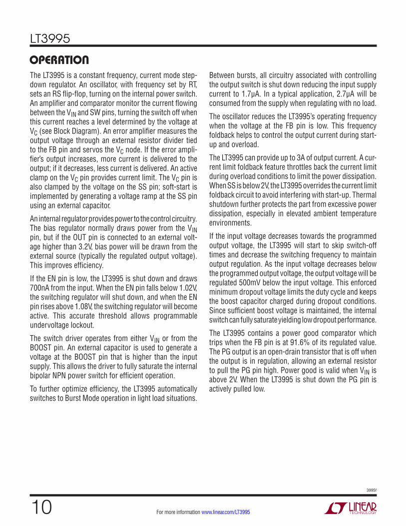
Load Transient: 0.5A to 2.5A Load Transient: 10mA to 2A
VOUT200mV/DIV
IL1A/DIV
20µs/DIVVIN = 48VVOUT = 3.3VCOUT = 47µF ×2
3995 G36
VOUT200mV/DIV
IL1A/DIV
20µs/DIVVIN = 48VVOUT = 3.3VCOUT = 47µF ×2
3995 G37

LT3995
93995f
For more information www.linear.com/LT3995
BLOCK DIAGRAM
+–
+–
+–
+–
OSCILLATOR200kHz TO 2MHz
Burst ModeDETECT
VC CLAMPVC
SLOPE COMP
R
VINVIN
EN BOOST
0.5V
SW
SHDN
SWITCHLATCH
SS1.8µA
VOUT
C2
C3
C4OPT
L1
D1
OUT
RT
R2
GND
ERROR AMP
R1
FB
RT
C1
PG
1.097V
1.02V
SQ
3995 BD
INTERNAL 1.197V REF
SYNC
+– SHDN +
C5
+–
LT3995
103995f
For more information www.linear.com/LT3995
OPERATIONThe LT3995 is a constant frequency, current mode step-down regulator. An oscillator, with frequency set by RT, sets an RS flip-flop, turning on the internal power switch. An amplifier and comparator monitor the current flowing between the VIN and SW pins, turning the switch off when this current reaches a level determined by the voltage at VC (see Block Diagram). An error amplifier measures the output voltage through an external resistor divider tied to the FB pin and servos the VC node. If the error ampli-fier’s output increases, more current is delivered to the output; if it decreases, less current is delivered. An active clamp on the VC pin provides current limit. The VC pin is also clamped by the voltage on the SS pin; soft-start is implemented by generating a voltage ramp at the SS pin using an external capacitor.
An internal regulator provides power to the control circuitry. The bias regulator normally draws power from the VIN pin, but if the OUT pin is connected to an external volt-age higher than 3.2V, bias power will be drawn from the external source (typically the regulated output voltage). This improves efficiency.
If the EN pin is low, the LT3995 is shut down and draws 700nA from the input. When the EN pin falls below 1.02V, the switching regulator will shut down, and when the EN pin rises above 1.08V, the switching regulator will become active. This accurate threshold allows programmable undervoltage lockout.
The switch driver operates from either VIN or from the BOOST pin. An external capacitor is used to generate a voltage at the BOOST pin that is higher than the input supply. This allows the driver to fully saturate the internal bipolar NPN power switch for efficient operation.
To further optimize efficiency, the LT3995 automatically switches to Burst Mode operation in light load situations.
Between bursts, all circuitry associated with controlling the output switch is shut down reducing the input supply current to 1.7μA. In a typical application, 2.7μA will be consumed from the supply when regulating with no load.
The oscillator reduces the LT3995’s operating frequency when the voltage at the FB pin is low. This frequency foldback helps to control the output current during start-up and overload.
The LT3995 can provide up to 3A of output current. A cur-rent limit foldback feature throttles back the current limit during overload conditions to limit the power dissipation. When SS is below 2V, the LT3995 overrides the current limit foldback circuit to avoid interfering with start-up. Thermal shutdown further protects the part from excessive power dissipation, especially in elevated ambient temperature environments.
If the input voltage decreases towards the programmed output voltage, the LT3995 will start to skip switch-off times and decrease the switching frequency to maintain output regulation. As the input voltage decreases below the programmed output voltage, the output voltage will be regulated 500mV below the input voltage. This enforced minimum dropout voltage limits the duty cycle and keeps the boost capacitor charged during dropout conditions. Since sufficient boost voltage is maintained, the internal switch can fully saturate yielding low dropout performance.
The LT3995 contains a power good comparator which trips when the FB pin is at 91.6% of its regulated value. The PG output is an open-drain transistor that is off when the output is in regulation, allowing an external resistor to pull the PG pin high. Power good is valid when VIN is above 2V. When the LT3995 is shut down the PG pin is actively pulled low.

LT3995
113995f
For more information www.linear.com/LT3995
APPLICATIONS INFORMATIONAchieving Ultralow Quiescent Current
To enhance efficiency at light loads, the LT3995 operates in low ripple Burst Mode operation, which keeps the out-put capacitor charged to the desired output voltage while minimizing the input quiescent current. In Burst Mode operation the LT3995 delivers single pulses of current to the output capacitor followed by sleep periods where the output power is supplied by the output capacitor. When in sleep mode the LT3995 consumes 1.7μA, but when it turns on all the circuitry to deliver a current pulse, the LT3995 consumes several mA of input current in addition to the switch current. Therefore, the total quiescent current will be greater than 1.7μA when regulating.
As the output load decreases, the frequency of single cur-rent pulses decreases (see Figure 1) and the percentage of time the LT3995 is in sleep mode increases, resulting in much higher light load efficiency. By maximizing the time between pulses, the converter quiescent current gets closer to the 1.7μA ideal. Therefore, to optimize the quiescent current performance at light loads, the current in the feedback resistor divider and the reverse current in the catch diode must be minimized, as these appear to the output as load currents. Use the largest possible feedback resistors and a low leakage Schottky catch diode in applications utilizing the ultralow quiescent current performance of the LT3995. The feedback resistors should preferably be on the order of MΩ and the Schottky catch diode should have less than a few µA of typical reverse leakage at room temperature. These two considerations are reiterated in the FB Resistor Network and Catch Diode Selection sections.
Figure 1. Switching Frequency in Burst Mode Operation
It is important to note that another way to decrease the pulse frequency is to increase the magnitude of each single current pulse. However, this increases the output voltage ripple because each cycle delivers more power to the output capacitor. The magnitude of the current pulses was selected to ensure less than 30mV of output ripple with one 47µF ceramic output capacitor in a typical ap-plication. See Figure 2.
Figure 2. Burst Mode Operation
While in Burst Mode operation, the burst frequency and the charge delivered with each pulse will not change with output capacitance. Therefore, the output voltage ripple will be inversely proportional to the output capacitance. In a typical application with two 47µF output capacitors, the output ripple is about 15mV, and with four 47µF output capacitors the output ripple is about 7.5mV. The output voltage ripple can continue to be decreased by increas-ing the output capacitance, though care must be taken to minimize the effects of output capacitor ESR and ESL.
At higher output loads (above 90mA for the front page application) the LT3995 will be running at the frequency programmed by the RT resistor, and will be operating in standard PWM mode. The transition between PWM and low ripple Burst Mode operation is seamless, and will not disturb the output voltage.
To ensure proper Burst Mode operation, the SYNC pin must be grounded. When synchronized with an external clock, the LT3995 will pulse skip at light loads. At very light loads, the part will go to sleep between groups of pulses, so the quiescent current of the part will still be low, but not as low as in Burst Mode operation. The quiescent current in a typical application when synchronized with an external LOAD CURRENT (mA)
050
SWIT
CHIN
G FR
EQUE
NCY
(kHz
)
100
200
300
400
600
20 40 60 803995 F01
100 120
500 VOUT = 5VfSW = 500kHz
L = 10µH
VOUT = 3.3VfSW = 300kHzL = 8.2µH
VIN = 12V
VSW20V/DIV
VOUT50mV/DIV
IL1A/DIV
5µs/DIVVIN = 48VVOUT = 3.3VILOAD = 70mACOUT = 47µF
3995 F02

LT3995
123995f
For more information www.linear.com/LT3995
APPLICATIONS INFORMATIONclock is 11µA. Holding the SYNC pin DC high yields no advantages in terms of output ripple or minimum load to full frequency, so is not recommended.
FB Resistor Network
The output voltage is programmed with a resistor divider between the output and the FB pin. Choose the resistor values according to:
R1= R2
VOUT1.197V
–1
Reference designators refer to the Block Diagram. 1% resistors are recommended to maintain output voltage accuracy.
The total resistance of the FB resistor divider should be selected to be as large as possible to enhance low current performance. The resistor divider generates a small load on the output, which should be minimized to optimize the low supply current at light loads.
When using large FB resistors, a 10pF phase lead capacitor should be connected from VOUT to FB.
Setting the Switching Frequency
The LT3995 uses a constant frequency PWM architecture that can be programmed to switch from 200kHz to 2MHz by using a resistor tied from the RT pin to ground. A table showing the necessary RT value for a desired switching frequency is in Table 1.
Table 1. Switching Frequency vs RT ValueSWITCHING FREQUENCY (MHz) RT VALUE (kΩ)
0.2 2940.3 1820.4 1300.6 78.70.8 54.91.0 41.21.2 32.41.4 26.11.6 21.51.8 17.82.0 14.72.2 12.4
To estimate the required RT value, use the following equation:
RT = 51.1
fSW( )1.09 – 9.27
where fSW is the desired switching frequency in MHz and RT is in kΩ.
Operating Frequency Trade-Offs
Selection of the operating frequency is a trade-off between efficiency, component size, minimum dropout voltage, and maximum input voltage. The advantage of high frequency operation is that smaller inductor and capacitor values may be used. The disadvantages are lower efficiency, and lower maximum input voltage. The highest acceptable switching frequency (fSW(MAX)) for a given application can be calculated as follows:
fSW(MAX) =
VOUT + VDtON(MIN) VIN – VSW + VD( )
where VIN is the typical input voltage, VOUT is the output voltage, VD is the catch diode drop (~0.5V), and VSW is the internal switch drop (~0.24V at max load). This equa-tion shows that slower switching frequency is necessary to safely accommodate high VIN/VOUT ratio. This is due to the limitation on the LT3995’s minimum on-time. The minimum on-time is a strong function of temperature. Use the typical minimum on-time curve to design for an application’s maximum temperature, while adding about 30% for part-to-part variation. The minimum duty cycle that can be achieved taking minimum on time into account is:
DCMIN = fSW • tON(MIN)
where fSW is the switching frequency, the tON(MIN) is the minimum switch on-time.
A good choice of switching frequency should allow ad-equate input voltage range (see next two sections) and keep the inductor and capacitor values small.
Maximum Input Voltage Range
The LT3995 can operate from input voltages of up to 60V. Often the highest allowed VIN during normal operation (VIN(OP-MAX)) is limited by the minimum duty cycle rather
LT3995
133995f
For more information www.linear.com/LT3995
APPLICATIONS INFORMATIONthan the absolute maximum ratings of the VIN pin. It can be calculated using the following equation:
VIN(OP-MAX) =
VOUT + VDfSW • tON(MIN)
– VD + VSW
where tON(MIN) is the minimum switch on-time. A lower switching frequency can be used to extend normal opera-tion to higher input voltages.
The circuit will tolerate inputs above the maximum op-erating input voltage and up to the absolute maximum ratings of the VIN and BOOST pins, regardless of chosen switching frequency. However, during such transients where VIN is higher than VIN(OP-MAX), the LT3995 will enter pulse-skipping operation where some switching pulses are skipped to maintain output regulation. The output voltage ripple and inductor current ripple will be higher than in typical operation. Do not overload when VIN is greater than VIN(OP-MAX).
Minimum Input Voltage Range
The minimum input voltage is determined by either the LT3995’s minimum operating voltage of 4.3V, its maximum duty cycle, or the enforced minimum dropout voltage. See the Typical Performance Characteristics section for the minimum input voltage across load for outputs of 3.3V and 5V.
The duty cycle is the fraction of time that the internal switch is on during a clock cycle. Unlike many fixed fre-quency regulators, the LT3995 can extend its duty cycle by remaining on for multiple clock cycles. The LT3995 will not switch off at the end of each clock cycle if there is sufficient voltage across the boost capacitor (C3 in the Block Diagram). Eventually, the voltage on the boost capacitor falls and requires refreshing. When this occurs, the switch will turn off, allowing the inductor current to recharge the boost capacitor. This places a limitation on the maximum duty cycle as follows:
DCMAX =
βSWβSW + 1
where βSW is equal to the beta of the internal power switch. The beta of the power switch is typically about 50, which leads to a DCMAX of about 98%. This leads to a minimum input voltage of approximately:
VIN(MIN1) =
VOUT + VDDCMAX
– VD + VSW
where VOUT is the output voltage, VD is the catch diode drop, VSW is the internal switch drop and DCMAX is the maximum duty cycle.
The final factor affecting the minimum input voltage is the minimum dropout voltage. When the OUT pin is tied to the output, the LT3995 regulates the output such that it stays 500mV below VIN. This enforced minimum drop-out voltage is due to reasons that are covered in the next section. This places a limitation on the minimum input voltage as follows:
VIN(MIN2) = VOUT + VDROPOUT(MIN)
where VOUT is the programmed output voltage and VDROPOUT(MIN) is the minimum dropout voltage of 500mV.
Combining these factors leads to the overall minimum input voltage:
VIN(MIN) = Max (VIN(MIN1), VIN(MIN2), 4.3V)
Minimum Dropout Voltage
To achieve a low dropout voltage, the internal power switch must always be able to fully saturate. This means that the boost capacitor, which provides a base drive higher than VIN, must always be able to charge up when the part starts up and then must also stay charged during all operating conditions.
During start-up if there is insufficient inductor current, such as during light load situations, the boost capacitor will be unable to charge. When the LT3995 detects that the boost capacitor is not charged, it activates a 100mA (typical) pull-down on the OUT pin. If the OUT pin is connected to the output, the extra load will increase the inductor current enough to sufficiently charge the boost capacitor. When the boost capacitor is charged, the current source turns off, and the part may re-enter Burst Mode operation.
LT3995
143995f
For more information www.linear.com/LT3995
APPLICATIONS INFORMATIONTo keep the boost capacitor charged regardless of load during dropout conditions, a minimum dropout voltage is enforced. When the OUT pin is tied to the output, the LT3995 regulates the output such that:
VIN – VOUT > VDROPOUT(MIN)
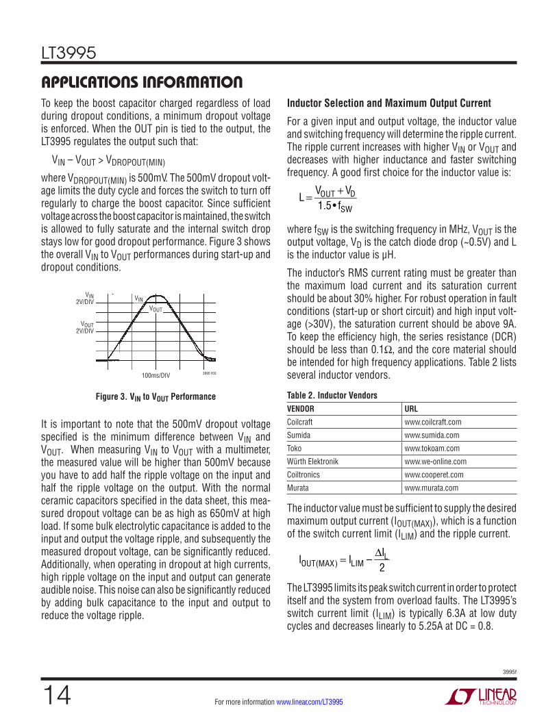
where VDROPOUT(MIN) is 500mV. The 500mV dropout volt-age limits the duty cycle and forces the switch to turn off regularly to charge the boost capacitor. Since sufficient voltage across the boost capacitor is maintained, the switch is allowed to fully saturate and the internal switch drop stays low for good dropout performance. Figure 3 shows the overall VIN to VOUT performances during start-up and dropout conditions.
Inductor Selection and Maximum Output Current
For a given input and output voltage, the inductor value and switching frequency will determine the ripple current. The ripple current increases with higher VIN or VOUT and decreases with higher inductance and faster switching frequency. A good first choice for the inductor value is:
L = VOUT + VD
1.5 • fSW
where fSW is the switching frequency in MHz, VOUT is the output voltage, VD is the catch diode drop (~0.5V) and L is the inductor value is μH.
The inductor’s RMS current rating must be greater than the maximum load current and its saturation current should be about 30% higher. For robust operation in fault conditions (start-up or short circuit) and high input volt-age (>30V), the saturation current should be above 9A. To keep the efficiency high, the series resistance (DCR) should be less than 0.1Ω, and the core material should be intended for high frequency applications. Table 2 lists several inductor vendors.
Table 2. Inductor VendorsVENDOR URL
Coilcraft www.coilcraft.com
Sumida www.sumida.com
Toko www.tokoam.com
Würth Elektronik www.we-online.com
Coiltronics www.cooperet.com
Murata www.murata.com
The inductor value must be sufficient to supply the desired maximum output current (IOUT(MAX)), which is a function of the switch current limit (ILIM) and the ripple current.
IOUT(MAX) = ILIM –
∆IL2
The LT3995 limits its peak switch current in order to protect itself and the system from overload faults. The LT3995’s switch current limit (ILIM) is typically 6.3A at low duty cycles and decreases linearly to 5.25A at DC = 0.8.
Figure 3. VIN to VOUT Performance
It is important to note that the 500mV dropout voltage specified is the minimum difference between VIN and VOUT. When measuring VIN to VOUT with a multimeter, the measured value will be higher than 500mV because you have to add half the ripple voltage on the input and half the ripple voltage on the output. With the normal ceramic capacitors specified in the data sheet, this mea-sured dropout voltage can be as high as 650mV at high load. If some bulk electrolytic capacitance is added to the input and output the voltage ripple, and subsequently the measured dropout voltage, can be significantly reduced. Additionally, when operating in dropout at high currents, high ripple voltage on the input and output can generate audible noise. This noise can also be significantly reduced by adding bulk capacitance to the input and output to reduce the voltage ripple.
VIN2V/DIV VIN
VOUT
VOUT2V/DIV
100ms/DIV 3995 F03

LT3995
153995f
For more information www.linear.com/LT3995
APPLICATIONS INFORMATIONWhen the switch is off, the potential across the inductor is the output voltage plus the catch diode drop. This gives the peak-to-peak ripple current in the inductor:
∆IL =
1–DC( ) • VOUT + VD( )L • fSW
where fSW is the switching frequency of the LT3995, DC is the duty cycle and L is the value of the inductor. Therefore, the maximum output current that the LT3995 will deliver depends on the switch current limit, the inductor value, and the input and output voltages. The inductor value may have to be increased if the inductor ripple current does not allow sufficient maximum output current (IOUT(MAX)) given the switching frequency, and maximum input voltage used in the desired application.
The optimum inductor for a given application may differ from the one indicated by this simple design guide. A larger value inductor provides a higher maximum load current and reduces the output voltage ripple. If your load is lower than the maximum load current, than you can relax the value of the inductor and operate with higher ripple current. This allows you to use a physically smaller inductor, or one with a lower DCR resulting in higher efficiency. Be aware that if the inductance differs from the simple rule above, then the maximum load current will depend on the input voltage. In addition, low inductance may result in discontinuous mode operation, which further reduces maximum load current. For details of maximum output current and discontinuous operation, see Linear Technology’s Application Note 44. Finally, for duty cycles greater than 50% (VOUT/VIN > 0.5), a minimum inductance is required to avoid sub-harmonic oscillations, see Application Note 19.
One approach to choosing the inductor is to start with the simple rule given above, look at the available induc-tors, and choose one to meet cost or space goals. Then use the equations above to check that the LT3995 will be able to deliver the required output current. Note again that these equations assume that the inductor current is continuous. Discontinuous operation occurs when IOUT is less than ΔIL/2.
Current Limit Foldback and Thermal Protection
The LT3995 has a large peak current limit to ensure a 3A max output current across duty cycle and current limit distribution, as well as allowing a reasonable inductor ripple current. During a short-circuit fault, having a large current limit can lead to excessive power dissipation and temperature rise in the LT3995, as well as the inductor and catch diode. To limit this power dissipation, the LT3995 starts to fold back the current limit when the FB pin falls below 0.8V. The LT3995 typically lowers the peak current limit about 50% from 6.3A to 3.1A when FB goes to 0V.
During start-up, when the output voltage and FB pin are low, current limit foldback could hinder the LT3995’s ability to start up into a large load. To avoid this potential problem, the LT3995’s current limit foldback will be disabled until the SS pin has charged above 2V. Therefore, the use of a soft-start capacitor will keep the current limit foldback feature out of the way while the LT3995 is starting up.
The LT3995 has thermal shutdown to further protect the part during periods of high power dissipation, particularly in high ambient temperature environments. The thermal shutdown feature detects when the LT3995 is too hot and shuts the part down, preventing switching. When the thermal event passes and the LT3995 cools, the part will restart and resume switching. A thermal shutdown event actively discharges the soft-start capacitor.
Input Capacitor
Bypass the input of the LT3995 circuit with a ceramic capaci-tor of X7R or X5R type. Y5V types have poor performance over temperature and applied voltage, and should not be used. A 4.7μF to 10μF ceramic capacitor is adequate to bypass the LT3995 and will easily handle the ripple cur-rent. Note that larger input capacitance is required when a lower switching frequency is used (due to longer on times). If the input power source has high impedance, or there is significant inductance due to long wires or cables, additional bulk capacitance may be necessary. This can be provided with a low performance electrolytic capacitor.

LT3995
163995f
For more information www.linear.com/LT3995
Step-down regulators draw current from the input sup-ply in pulses with very fast rise and fall times. The input capacitor is required to reduce the resulting voltage ripple at the LT3995 and to force this very high frequency switching current into a tight local loop, minimizing EMI. A 4.7μF capacitor is capable of this task, but only if it is placed close to the LT3995 (see the PCB Layout section). A second precaution regarding the ceramic input capacitor concerns the maximum input voltage rating of the LT3995. A ceramic input capacitor combined with trace or cable inductance forms a high quality (under damped) tank circuit. If the LT3995 circuit is plugged into a live supply, the input voltage can ring to twice its nominal value, pos-sibly exceeding the LT3995’s voltage rating. If the input supply is poorly controlled or the user will be plugging the LT3995 into an energized supply, the input network should be designed to prevent this overshoot. See Linear Technology Application Note 88 for a complete discussion.
Output Capacitor and Output Ripple
The output capacitor has two essential functions. Along with the inductor, it filters the square wave generated by the LT3995 to produce the DC output. In this role it determines the output ripple, so low impedance (at the switching frequency) is important. The second function is to store energy in order to satisfy transient loads and stabilize the LT3995’s control loop. Ceramic capacitors have very low equivalent series resistance (ESR) and provide the best ripple performance. A good starting value is:
COUT = 200
VOUT • fSW
where fSW is in MHz, and COUT is the recommended output capacitance in μF. Use X5R or X7R types. This choice will provide low output ripple and good transient response. Transient performance can be improved with a higher value capacitor if combined with a phase lead capacitor (typically 10pF) between the output and the feedback pin. A lower value of output capacitor can be used to save space and cost but transient performance will suffer.
When choosing a capacitor, look carefully through the data sheet to find out what the actual capacitance is under
operating conditions (applied voltage and temperature). A physically larger capacitor or one with a higher voltage rating may be required. Table 3 lists several capacitor vendors.
Table 3. Recommended Ceramic Capacitor VendorsMANUFACTURER URL
AVX www.avxcorp.com
Murata www.murata.com
Taiyo Yuden www.t-yuden.com
Vishay Siliconix www.vishay.com
TDK www.tdk.com
Ceramic Capacitors
When in dropout, the LT3995 can excite ceramic capacitors at audio frequencies. At high load, this could be unaccept-able. Simply adding bulk input capacitance to the input and output will significantly reduce the voltage ripple and the audible noise generated at these nodes to acceptable levels.
A final precaution regarding ceramic capacitors concerns the maximum input voltage rating of the LT3995. As pre-viously mentioned, a ceramic input capacitor combined with trace or cable inductance forms a high quality (under damped) tank circuit. If the LT3995 circuit is plugged into a live supply, the input voltage can ring to twice its nominal value, possibly exceeding the LT3995’s rating. If the input supply is poorly controlled or the user will be plugging the LT3995 into an energized supply, the input network should be designed to prevent this overshoot. See Linear Technology Application Note 88 for a complete discussion.
Catch Diode Selection
The catch diode (D1 from the Block Diagram) conducts current only during the switch off time. Average forward current in normal operation can be calculated from:
ID(AVG) = IOUT
VIN – VOUTVIN
where IOUT is the output load current. The current rating of the diode should be selected to be greater than or equal to the application’s output load current, so that the diode is
APPLICATIONS INFORMATION

LT3995
173995f
For more information www.linear.com/LT3995
robust for a wide input voltage range. A diode with even higher current rating can be selected for the worst-case scenario of overload, where the max diode current can then increase to the typical peak switch current. Short circuit is not the worst-case condition due to current limit foldback. Peak reverse voltage is equal to the regulator input voltage. For inputs up to 60V, a 60V diode is adequate.
An additional consideration is reverse leakage current. When the catch diode is reversed biased, any leakage current will appear as load current. When operating under light load conditions, the low supply current consumed by the LT3995 will be optimized by using a catch diode with minimum reverse leakage current. Low leakage Schottky diodes often have larger forward voltage drops at a given current, so a trade-off can exist between low load and high load efficiency. Often Schottky diodes with larger reverse bias ratings will have less leakage at a given output voltage than a diode with a smaller reverse bias rating. Therefore, superior leakage performance can be achieved at the expense of diode size. Table 4 lists several Schottky diodes and their manufacturers.
BOOST and OUT Pin Considerations
Capacitor C3 and the internal boost Schottky diode (see the Block Diagram) are used to generate a boost voltage that is higher than the input voltage. In most cases a 0.47μF capacitor will work well. The BOOST pin must be more than 1.8V above the SW pin for best efficiency and more than 2.6V above the SW pin to allow the LT3995 to skip off times to achieve very high duty cycles. For outputs between 3.2V and 16V, the standard circuit with the OUT pin connected to the output (Figure 4a) is best. Below 3.2V the internal Schottky diode may not be able to sufficiently charge the boost capacitor. Above 16V, the OUT pin abs max is violated. For outputs between 2.5V and 3.2V, an external Schottky diode to the output is sufficient because an external Schottky will have much lower forward voltage drop than the internal boost diode.
APPLICATIONS INFORMATIONTable 4. Schottky Diodes. The Reverse Current Values Listed Are Estimates Based Off of Typical Curves for Reverse Current vs Reverse Voltage at 25°C
PART NUMBER VR (V) IAVE (A)
VF at 3A TYP 25°C
(mV)
VF at 3A MAX
25°C (mV)
IR at VR = 20V
25°C (µA)
PDS360 60 3 570 620 0.45
PDS560 60 5 540 0.9
B360A 60 3 600 700 50
SBR3U60P1 60 3 580 650 1.7
For output voltages less than 2.5V, there are two options. An external Schottky diode can charge the boost capaci-tor from the input (Figure 4c) or from an external voltage source (Figure 4d). Using an external voltage source is the better option because it is more efficient than charging the boost capacitor from the input. However, such a voltage rail is not always available in all systems. For output volt-ages greater than 16V, an external Schottky diode from an external voltage source should be used to charge the boost capacitor (Figure 4e). In applications using an ex-ternal voltage source, the supply should be between 3.1V and 16V. When using the input, the input voltage may not exceed 30V. In all cases, the maximum voltage rating of the BOOST pin must not be exceeded.
When the output is above 16V, the OUT pin can not be tied to the output or the OUT pin abs max will be violated. It should instead be tied to GND (Figure 4e). This is to pre-vent the dropout circuitry from interfering with switching behavior and to prevent the 100mA active pull-down from drawing power. It is important to note that when the output is above 16V and the OUT pin is grounded, the dropout circuitry is not connected, so the minimum dropout will be about 1.5V, rather than 500mV. If the output is less than 3.2V and an external Schottky is used to charge the boost capacitor, the OUT pin should still be tied to the output even though the minimum input voltage of the LT3995 will be limited by the 4.3V minimum rather than the minimum dropout voltage.

LT3995
183995f
For more information www.linear.com/LT3995
With the OUT pin connected to the output, a 100mA ac-tive load will charge the boost capacitor during light load start-up and an enforced 500mV minimum dropout voltage will keep the boost capacitor charged across operating conditions (see Minimum Dropout Voltage section). This yields excellent start-up and dropout performance. Figure 5 shows the minimum input voltage for 3.3V and 5V outputs.
Enable and Undervoltage Lockout
The LT3995 is in shutdown when the EN pin is low and active when the pin is high. The falling threshold of the EN comparator is 1.02V, with 60mV of hysteresis. The EN pin can be tied to VIN if the shutdown feature is not used.
Undervoltage lockout (UVLO) can be added to the LT3995 as shown in Figure 6. Typically, UVLO is used in situa-
APPLICATIONS INFORMATION
Figure 5. The Minimum Input Voltage Depends on Output Voltage and Load Current
BOOST
LT3995
(4a) For 3.2V ≤ VOUT ≤ 16V
GND
VINVIN SW
OUT VOUT
BOOST
LT3995
(4d) For VOUT < 2.5V, 3.1V ≤ VS ≤ 16V
GND
VINVIN SW
OUT VOUT
VS
BOOST
LT3995
(4e) For VOUT > 16V, 3.1V ≤ VS ≤ 16V
GND
VINVIN SW
OUT VOUT
3995 F04
VS
BOOST
LT3995
(4c) For VOUT < 2.5V, VIN < 30V
GND
VINVIN SW
OUT VOUT
BOOST
LT3995
(4b) For 2.5V ≤ VOUT ≤ 3.2V
GND
VINVIN SW
OUT VOUT
Figure 4. Five Circuits for Generating the Boost Voltage
Minimum Input Voltage, VOUT = 5V Minimum Input Voltage, VOUT = 3.3V
LOAD CURRENT (A)0
4.0
INPU
T VO
LTAG
E (V
)
4.5
5.0
5.5
6.0
6.5
0.5 1.0 1.5 2.0
3995 F05a
2.5 3.0
VOUT = 5VfSW = 500kHz
TO RUN/TO START
LOAD CURRENT (A)0
2.5
INPU
T VO
LTAG
E (V
)
3.0
3.5
4.0
4.5
5.0
0.5 1.0 1.5 2.0
3995 F05b
2.5 3.0
VOUT = 3.3VFRONT PAGE APPLICATION
TO RUN/TO START
LT3995
193995f
For more information www.linear.com/LT3995
tions where the input supply is current limited, or has a relatively high source resistance. A switching regulator draws constant power from the source, so source cur-rent increases as source voltage drops. This looks like a negative resistance load to the source and can cause the source to current limit or latch low under low source voltage conditions. UVLO prevents the regulator from operating at source voltages where the problems might occur. The UVLO threshold can be adjusted by setting the values R3 and R4 such that they satisfy the following equation:
VUVLO = VEN(THRESH)
R3 + R4R4
where VEN(THRESH) is the falling threshold of the EN pin, which is approximately 1.02V, and where switching should stop when VIN falls below VUVLO. Note that due to the comparator’s hysteresis, switching will not start until the input is about 6% above VUVLO.
When operating in Burst Mode operation for light load currents, the current through the UVLO resistor network can easily be greater than the supply current consumed by the LT3995. Therefore, the UVLO resistors should be large to minimize their effect on efficiency at low loads.
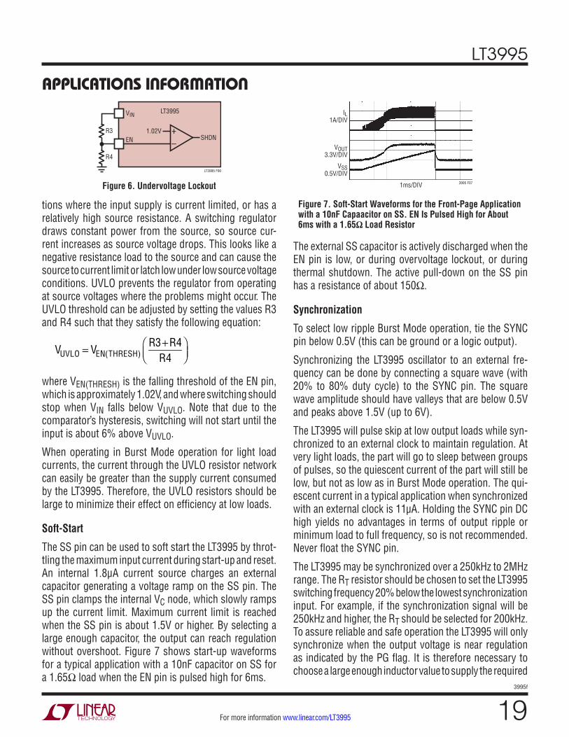
Soft-Start
The SS pin can be used to soft start the LT3995 by throt-tling the maximum input current during start-up and reset. An internal 1.8μA current source charges an external capacitor generating a voltage ramp on the SS pin. The SS pin clamps the internal VC node, which slowly ramps up the current limit. Maximum current limit is reached when the SS pin is about 1.5V or higher. By selecting a large enough capacitor, the output can reach regulation without overshoot. Figure 7 shows start-up waveforms for a typical application with a 10nF capacitor on SS for a 1.65Ω load when the EN pin is pulsed high for 6ms.
APPLICATIONS INFORMATION
SHDN1.02V
EN
LT3995VIN
R3
R4
LT3995 F06
+–
Figure 6. Undervoltage Lockout
Figure 7. Soft-Start Waveforms for the Front-Page Application with a 10nF Capaacitor on SS. EN Is Pulsed High for About 6ms with a 1.65Ω Load Resistor
VOUT3.3V/DIV
VSS0.5V/DIV
IL1A/DIV
1ms/DIV 3995 F07
The external SS capacitor is actively discharged when the EN pin is low, or during overvoltage lockout, or during thermal shutdown. The active pull-down on the SS pin has a resistance of about 150Ω.
Synchronization
To select low ripple Burst Mode operation, tie the SYNC pin below 0.5V (this can be ground or a logic output).
Synchronizing the LT3995 oscillator to an external fre-quency can be done by connecting a square wave (with 20% to 80% duty cycle) to the SYNC pin. The square wave amplitude should have valleys that are below 0.5V and peaks above 1.5V (up to 6V).
The LT3995 will pulse skip at low output loads while syn-chronized to an external clock to maintain regulation. At very light loads, the part will go to sleep between groups of pulses, so the quiescent current of the part will still be low, but not as low as in Burst Mode operation. The qui-escent current in a typical application when synchronized with an external clock is 11µA. Holding the SYNC pin DC high yields no advantages in terms of output ripple or minimum load to full frequency, so is not recommended. Never float the SYNC pin.
The LT3995 may be synchronized over a 250kHz to 2MHz range. The RT resistor should be chosen to set the LT3995 switching frequency 20% below the lowest synchronization input. For example, if the synchronization signal will be 250kHz and higher, the RT should be selected for 200kHz. To assure reliable and safe operation the LT3995 will only synchronize when the output voltage is near regulation as indicated by the PG flag. It is therefore necessary to choose a large enough inductor value to supply the required

LT3995
203995f
For more information www.linear.com/LT3995
output current at the frequency set by the RT resistor (see Inductor Selection section). The slope compensation is set by the RT value, while the minimum slope compensation required to avoid subharmonic oscillations is established by the inductor size, input voltage and output voltage. Since the synchronization frequency will not change the slopes of the inductor current waveform, if the inductor is large enough to avoid subharmonic oscillations at the frequency set by RT, than the slope compensation will be sufficient for all synchronization frequencies.
Power Good Flag
The PG pin is an open-drain output which is used to indicate to the user when the output voltage is within regulation. When the output is lower than the regulation voltage by more than 8.4%, as determined from the FB pin voltage, the PG pin will pull low to indicate the power is not good. Otherwise, the PG pin will go high impedance and can be pulled logic high with a resistor pull-up. The PG pin is only comparing the output voltage to an accurate refer-ence when the LT3995 is enabled and VIN is above 4.3V. When the part is shutdown, the PG is actively pulled low to indicate that the LT3995 is not regulating the output. The input voltage must be greater than 1.4V to fully turn-on the active pull-down device. Figure 8 shows the status of the PG pin as the input voltage is increased.
APPLICATIONS INFORMATION
Figure 8. PG Pin Voltage Versus Input Voltage when PG Is Connected to 3V Through a 150k Resistor. The FB Pin Voltage Is 1.15V
INPUT VOLTAGE (V)0
PG P
IN V
OLTA
GE (V
)
2
3
4
3995 F08
1
01 2 2.5 5
4
30.5 1.5 4.53.5
VIN BOOSTVIN
EN
3995 F09
VOUT
BACKUP
LT3995
D4PDS360
SW
OUTGND FB +
Figure 9. Diode D4 Prevents a Shorted Input from Discharging a Backup Battery Tied to the Output. It Also Protects the Circuit from a Reversed Input. The LT3995 Runs Only When the Input Is Present
Shorted and Reversed Input Protection
If the inductor is chosen so that it won’t saturate excessively, a LT3995 buck regulator will tolerate a shorted output and the power dissipation will be limited by current limit fold-back (see Current Limit Foldback and Thermal Protection section). There is another situation to consider in systems where the output will be held high when the input to the LT3995 is absent. This may occur in battery charging ap-plications or in battery backup systems where a battery or some other supply is diode ORed with the LT3995’s output. If the VIN pin is allowed to float and the EN/UVLO pin is held high (either by a logic signal or because it is tied to VIN), then the LT3995’s internal circuitry will pull its quiescent current through its SW pin. This is fine if your system can tolerate a few μA in this state. If you ground the EN pin, the SW pin current will drop to essentially zero. However, if the VIN pin is grounded while the output is held high, regardless of EN, parasitic diodes inside the LT3995 can pull current from the output through the SW pin and the VIN pin. Figure 9 shows a circuit that will run only when the input voltage is present and that protects against a shorted or reversed input.

LT3995
213995f
For more information www.linear.com/LT3995
these layers will spread the heat dissipated by the LT3995. Placing additional vias can reduce the thermal resistance further. When operating at high ambient temperatures, the maximum load current should be derated as the ambient temperature approaches the maximum junction rating. (See the Thermal Derating curve in the Typical Performance Characteristics section.)
Power dissipation within the LT3995 can be estimated by calculating the total power loss from an efficiency measure-ment and subtracting the catch diode loss and inductor loss. The die temperature is calculated by multiplying the LT3995 power dissipation by the thermal resistance from junction to ambient. The temperature rise of the LT3995 for a 3.3V and 5V application is measured using a thermal camera and is shown in Figure 11.
APPLICATIONS INFORMATION
Figure 10. Layout Showing a Good PCB Design
PCB Layout
For proper operation and minimum EMI, care must be taken during printed circuit board layout. Figure 10 shows a sample component placement with trace, ground plane and via locations, which serves as a good PCB layout example. Note that large, switched currents flow in the LT3995’s VIN and SW pins, the catch diode (D1), and the input capacitor (C1). The loop formed by these compo-nents should be as small as possible. These components, along with the inductor and output capacitor, should be placed on the same side of the circuit board, and their connections should be made on that layer. Place a local, unbroken ground plane below these components. The SW and BOOST nodes should be as small as possible. Finally, keep the FB and RT nodes small so that the ground traces will shield it from the SW and BOOST nodes. The exposed pad on the bottom of the package must be soldered to ground so that the pad acts as a heat sink. To keep thermal resistance low, extend the ground plane as much as pos-sible, and add thermal vias under and near the LT3995 to additional ground planes within the circuit board and on the bottom side.
VOUT
VIN
3995 F10
VOUTRT
PGFB •• •• ••• • •• • •• • •• • •• • •• • •• • •• • •• • •
OUT
SW
EN
BST
17
SS SYNC
High Temperature Considerations
For higher ambient temperatures, care should be taken in the layout of the PCB to ensure good heat sinking of the LT3995. The exposed pad on the bottom of the package must be soldered to a ground plane. This ground should be tied to large copper layers below with thermal vias;
OUTPUT CURRENT (A)1
40
50
70
2.5
3395 F11a
30
20
1.5 2 3
10
0
60CH
IP T
EMPE
RATU
RE R
ISE
(°C)
12V24V36V48V60V
VOUT = 3.3VfSW = 300kHz2.5in x 2.5in 4-LAYER BOARD
OUTPUT CURRENT (A)1
CHIP
TEM
PERA
TURE
RIS
E (°
C)
50
60
70
3
3995 F11b
40
30
20
01.5 2 2.5
10
90
80
12V24V36V48V60V
VOUT = 5VfSW = 500kHz2.5in x 2.5in 4-LAYER BOARD
Figure 11a. Temperature Rise of the LT3995 in the Front Page Application
Figure 11b. Temperature Rise of the LT3995 in a 5VOUT Application

LT3995
223995f
For more information www.linear.com/LT3995
TYPICAL APPLICATIONS4V Step-Down Converter with a High Impedance Input Source
2.5V Step-Down Converter
VIN
PG BOOST
EN0.47µF
PDS360
47µF1210×2
3995 TA05
47nF
CBULK100µF
24V
10µF
432k
f = 800kHz
54.9k
499k
5.49M
VOUT4V3A
4.7µH
LT3995
SS
RT
SW
OUT
FBSYNC GND
1M
10pF
+
V
+
–
VIN
EN
BOOST
OFF ON
VIN4.3V TO 60V
PG
0.47µF
47µF1210×2
3995 TA06
10nF
10µF
909k
f = 250kHz
226k
VOUT2.5V3A
10µH
LT3995
SS
RT
SW
OUT
FBSYNC GND
1M
10pF
PDS360
5V Step-Down Converter
12V Step-Down Converter
VIN
EN BOOSTOFF ON
VIN5.7V TO 60V
PG0.47µF
PDS360
22µF1210×2
3975 TA02
10nF
10µF
316k
f = 500kHz
97.6k
VOUT5V3A
6.8µH
LT3995
SS
RT
SW
OUT
FBSYNC GND
1M
10pF
VIN
EN BOOSTOFF ON
VIN12.9V TO 60V
PG0.47µF
22µF1210×2
3995 TA03
10nF
10µF
110k
f = 800kHz
54.9k
VOUT12V2.5A (3A TRANSIENTS)
10µH
LT3995
SS
RT
SW
OUT
FBSYNC GND
1M
10pF
PDS360
APPLICATIONS INFORMATIONAlso keep in mind that the leakage current of the power Schottky diode goes up exponentially with junction tem-perature. When the power switch is off, the power Schottky diode is in parallel with the power converter’s output filter stage. As a result, an increase in a diode’s leakage current results in an effective increase in the load, and a corresponding increase in the input quiescent current. Therefore, the catch Schottky diode must be selected with care to avoid excessive increase in light load supply current at high temperatures.
Other Linear Technology Publications
Application Notes 19, 35 and 44 contain more detailed descriptions and design information for buck regulators and other switching regulators. The LT1376 data sheet has a more extensive discussion of output ripple, loop compensation and stability testing. Design Note 318 shows how to generate a bipolar output supply using a buck regulator.
LT3995
233995f
For more information www.linear.com/LT3995
Information furnished by Linear Technology Corporation is believed to be accurate and reliable. However, no responsibility is assumed for its use. Linear Technology Corporation makes no representa-tion that the interconnection of its circuits as described herein will not infringe on existing patent rights.
PACKAGE DESCRIPTIONPlease refer to http://www.linear.com/designtools/packaging/ for the most recent package drawings.
MSOP (MSE16) 0911 REV E
0.53 ±0.152(.021 ±.006)
SEATINGPLANE
0.18(.007)
1.10(.043)MAX
0.17 – 0.27(.007 – .011)
TYP
0.86(.034)REF
0.50(.0197)
BSC
16
16151413121110
1 2 3 4 5 6 7 8
9
9
1 8
NOTE:1. DIMENSIONS IN MILLIMETER/(INCH)2. DRAWING NOT TO SCALE3. DIMENSION DOES NOT INCLUDE MOLD FLASH, PROTRUSIONS OR GATE BURRS. MOLD FLASH, PROTRUSIONS OR GATE BURRS SHALL NOT EXCEED 0.152mm (.006") PER SIDE4. DIMENSION DOES NOT INCLUDE INTERLEAD FLASH OR PROTRUSIONS. INTERLEAD FLASH OR PROTRUSIONS SHALL NOT EXCEED 0.152mm (.006") PER SIDE5. LEAD COPLANARITY (BOTTOM OF LEADS AFTER FORMING) SHALL BE 0.102mm (.004") MAX6. EXPOSED PAD DIMENSION DOES INCLUDE MOLD FLASH. MOLD FLASH ON E-PAD SHALL NOT EXCEED 0.254mm (.010") PER SIDE.
0.254(.010) 0° – 6° TYP
DETAIL “A”
DETAIL “A”
GAUGE PLANE
5.23(.206)MIN
3.20 – 3.45(.126 – .136)
0.889 ±0.127(.035 ±.005)
RECOMMENDED SOLDER PAD LAYOUT
0.305 ±0.038(.0120 ±.0015)
TYP
0.50(.0197)
BSC
BOTTOM VIEW OFEXPOSED PAD OPTION
2.845 ±0.102(.112 ±.004)
2.845 ±0.102(.112 ±.004)
4.039 ±0.102(.159 ±.004)
(NOTE 3)
1.651 ±0.102(.065 ±.004)
1.651 ±0.102(.065 ±.004)
0.1016 ±0.0508(.004 ±.002)
3.00 ±0.102(.118 ±.004)
(NOTE 4)
0.280 ±0.076(.011 ±.003)
REF
4.90 ±0.152(.193 ±.006)
DETAIL “B”
DETAIL “B”CORNER TAIL IS PART OF
THE LEADFRAME FEATURE.FOR REFERENCE ONLY
NO MEASUREMENT PURPOSE
0.12 REF
0.35REF
MSE Package16-Lead Plastic MSOP, Exposed Die Pad
(Reference LTC DWG # 05-08-1667 Rev E)

LT3995
243995f
For more information www.linear.com/LT3995 LINEAR TECHNOLOGY CORPORATION 2013
LT 0513 • PRINTED IN USA
RELATED PARTS
TYPICAL APPLICATION
PART NUMBER DESCRIPTION COMMENTS
LT3975 42V, 2.5A, 2MHz High Efficiency Micropower Step-Down DC/DC Converter with IQ = 2.7µA
VIN: 4.3V to 40V, VOUT(MIN) = 1.2V, IQ = 2.8µA, ISD < 1µA, MSOP-16E Package
LT3976 40V, 5A, 2MHz High Efficiency Micropower Step-Down DC/DC Converter with IQ = 3.3µA
VIN: 4.3V to 40V, VOUT(MIN) = 1.2V, IQ = 2.8µA, ISD < 1µA, MSOP-16E Package
LT3970 40V, 350mA, 2.2MHz High Efficiency Micropower Step-Down DC/DC Converter with IQ = 2.5µA
VIN: 4.2V to 40V, VOUT(MIN) = 1.21V, IQ = 2.5µA, ISD < 1µA, 3mm × 2mm DFN-10, MSOP-10 Packages
LT3990 62V, 350mA, 2.2MHz High Efficiency Micropower Step-Down DC/DC Converter with IQ = 2.5µA
VIN: 4.2V to 62V, VOUT(MIN) = 1.21V, IQ = 2.5µA, ISD < 1µA, 3mm × 2mm DFN-10, MSOP-10 Packages
LT3971 38V, 1.2A, 2.2MHz High Efficiency Micropower Step-Down DC/DC Converter with IQ = 2.8µA
VIN: 4.3V to 38V, VOUT(MIN) = 1.2V, IQ = 2.8µA, ISD < 1µA, 3mm × 3mm DFN-10, MSOP-10E Packages
LT3991 55V, 1.2A, 2.2MHz High Efficiency Micropower Step-Down DC/DC Converter with IQ = 2.8µA
VIN: 4.3V to 55V, VOUT(MIN) = 1.2V, IQ = 2.8µA, ISD < 1µA, 3mm × 3mm DFN-10, MSOP-10E Packages
LT8611 42V, 2.5A, 96% Efficiency, 2.2MHz Synchronous Micropower Step-Down DC/DC Converter with IQ = 2.5µA and Input/Output Current Limit/Monitor
VIN: 3.4V to 42V, VOUT(MIN) = 0.985V, IQ = 2.5µA, ISD < 1µA, 3mm × 5mm QFN-24 Package
LT8610 42V, 2.5A, 96% Efficiency, 2.2MHz Synchronous Micropower Step-Down DC/DC Converter with IQ = 2.5µA and Input/Output Current Limit/Monitor
VIN: 3.4V to 42V, VOUT(MIN) = 0.985V, IQ = 2.5µA, ISD < 1µA, MSOP-16E Package
LT3480 36V with Transient Protection to 60V, 2A (IOUT), 2.4MHz, High Efficiency Step-Down DC/DC Converter with Burst Mode Operation
VIN: 3.6V to 36V Transient to 60V, VOUT(MIN) = 0.78V, IQ = 70µA, ISD < 1µA, 3mm × 3mm DFN-10, MSOP-10E Packages
LT3980 58V with Transient Protection to 80V, 2A (IOUT), 2.4MHz, High Efficiency Step-Down DC/DC Converter with Burst Mode Operation
VIN: 3.6V to 58V Transient to 80V, VOUT(MIN) = 0.78V, IQ = 85µA, ISD < 1µA, 3mm × 4mm DFN-16, MSOP-16E Packages
5V, 2MHz Step-Down Converter with Power Good
VIN
EN
BOOST
OFF ON
VIN5.9V TO 16VTRANSIENT
TO 60V)0.47µF
47µF1210
3995 TA04
10nF
4.7µF
316k
150k
f = 2MHz
14.7k
VOUT5V3A
PGOOD
2.2µH
LT3995
SS
RT
SW
OUTPG
FBSYNC GND
1M
10pF
PDS360
Linear Technology Corporation1630 McCarthy Blvd., Milpitas, CA 95035-7417(408) 432-1900 ● FAX: (408) 434-0507 ● www.linear.com/LT3995