Low temperature microscopy of organic optoelectronic materials
52
Transcript of Low temperature microscopy of organic optoelectronic materials

Low temperature microscopy of organic
optoelectronic materials
Mattson Thieme
Thesis submitted to
Oregon State University
in partial ful�lment for the award of the degree of
Bachelor of Science
Physics
Option: Optical Physics
Department of Physics
301 Weniger Hall, Corvallis, OR 97331-6507


Abstract
We present a report on a new capability for low temperature microscopy of organic optoelec-
tronic semiconductor materials. We may now perform photoluminescence (PL) and conductivity
measurements as a function of temperature on a microscopic level. Testing con�rmed the setup's
ability to support microscopic measurements at pressures of ≈ 10−6 Torr and temperatures down
to 78K. Preliminary results on high performance ADT-TES-F composite materials have been ob-
tained including PL, of single crystals as well as donor-acceptor (D/A) spincast �lms, and images
of microscopic D/A domains under 60-100X magni�cation. An increase in PL was observed with
decreasing temperature in single crystals of ADT-TES-F due to a decrease in thermally activated
non-radiative recombination. Microscopic images of spincast D/A composites have yielded evidence
of exciplex formation at the grain boundaries, indicative of the presence of charge transfer states in
these regions.
Keywords: Organic semiconductor, low temperature, microscopy, exciplex, D/A domains.


Acknowledgements
This thesis would not have been possible without the loving, encouraging, and supportive people I
have had the privilege of sharing my life with.
I owe a most sincere thanks to my advisor, Dr. Oksana Ostroverkhova, for welcoming me into the
group, her boundless support, and for her steadfast dedication to my progression as a physicist, a
writer, and an individual. I also thank her for introducing me to Dr. Keshab Paudel, who devoted
countless hours in the lab to furthering my understanding of experimental techniques, and provided
me with the con�dence to work independently. I would also like to thank Dr. Janet Tate, whose
cheerful presence made for an exceptional introduction to scienti�c writing. In addition to Dr. Tate,
I was accorded with a vibrant and invested faculty whose didactic approach fostered a culture of
belonging and growth. I could not ask for a higher quality group of individuals on which to model
my behavior as a physicist. I would also like to thank the Oregon State University Research O�ce
for their funding under the URISC undergraduate research grant, which allowed me the freedom to
focus on research.
I would not be here without my family; the emotional and intellectual nourishment I receive from
their support, encouragement, and equanimity permeates every aspect of my life. And �nally, to
my dearest Kristin: that you share this journey with me is my greatest happiness.
1


List of Figures
1.1 Electronic energy levels of donor and acceptor molecules obtained via di�erential
pulse voltammetry. A Frenkel exciton is aligned vertically between the HOMO and
LUMO of the donor molecule. The arrow indicates a transition to a CT exciton,
shown bridging the gap between the LUMO of the acceptor and the HOMO of the
donor. . . . . . . . . . . . . . . . . . . . . . . . . . . . . . . . . . . . . . . . . . . . . 8
1.2 PL from Pristine ADT-TES-F and 95/5 ADT-TES-F/Pn-TIPS-F8 composite at room
temperature. Energy level inset shows origin of peaks in PL. . . . . . . . . . . . . . . 9
1.3 Absorption and PL of 90/10 ADT-TESF/PCBM thin �lm. S0, S1 represent the
ground and �rst excited excitonic states respectively; 0,1,2: vibronic states within
each level. Color-coded arrows overlaying the vibronic states indicate electron tran-
sitions leading to the absorption/emission peaks shown. . . . . . . . . . . . . . . . . 9
1.4 Molecular structures of (top left) the donor ADT-R-F, (right side) acceptors TES,
TSBS, TIPS, TCHS, and (bottom left) Pn-R-F8.[1] . . . . . . . . . . . . . . . . . . . 11
1.5 aMeasured by di�erential pulse voltammetry [39,45 of JphysChem]. bMeasured in
toluene. cMeasured in chlorobenzene. dMeasured in thin �lms spin-cast on PFBT
treated substrates.eCalculated from crystallographic data.[1] . . . . . . . . . . . . . . 11
2.1 Both images taken with 10X objective. LEFT: ADT-TSBS-F crystals grown on an
IGE pari, dark horizontal lines are gold electrodes. RIGHT: ADT-TESF/Pn-TIPS-
F8 thin �lm on quartz cover slip. . . . . . . . . . . . . . . . . . . . . . . . . . . . . . 13
2

LIST OF FIGURES LIST OF FIGURES
2.2 95/5 ADT-TES-F/Pn-TIPS-F8 composite PL overlaid with dark regions to demon-
strate wavelengths being �ltered out. Left: a 540LP and 640SP combine to allow only
the donor emission to be imaged. Right: a 680LP �lter removes the donor emission
and allows for all the exciplex emission to pass. . . . . . . . . . . . . . . . . . . . . . 20
3.1 Sample holder for electrical measurements or back illuminated PL in the minicryo-
stat. The sample may be translated 5 mm toward or away from the lower quartz
window to accomodate varying objective working distances. Components shown are
the following: 1. Substrate. 2. IGE. 3. Gold radiation shielding. 4. Microscope
objective. 5. Quartz windows. 6. Gold leads to IGE. 7. Copper mount. 8. Sample
holder base. 9. To Keithley Source Measure Unit. 10. Exterior walls of the cryostat. 23
3.2 98/2 ADT-TES-F/PCBM dark current taken inside the minicryostat at 10−6 Torr. . 24
3.3 80/20 ADT-TES-F/Pn-TIPS-F8 images under 60X magni�cation: Left - 540SP and
640LP �lter to isolate donor domains, Right - 680LP �lter to isolate exciplex formation. 25
3.4 MiniCryostat mounted atop the Olympus inverted microscope. In this diagram, the
sample is inside the MiniCryostat and its optical image is shown on the computer.
This image was a 95/5 ADT-TES-F/IF-MES sample spincast onto an IGE pair taken
with a 100X objective. . . . . . . . . . . . . . . . . . . . . . . . . . . . . . . . . . . 26
3.5 Absorption spectra for pristine ADT-TES-F as well as 95/5% ADT-TES-F/Pn-TIPS-
F8, /Pn-TCHS-F8. . . . . . . . . . . . . . . . . . . . . . . . . . . . . . . . . . . . . . 27
3.6 Bulk transient PL of exciplex emission in ADT-TES-F/Pn-TIPS-F8 and ADT-TES-
F/Pn-TCHS-F8 composites. . . . . . . . . . . . . . . . . . . . . . . . . . . . . . . . . 28
3.7 Transient photocurrent obtained under 355 nm 500 ps photoexcitation of a pristine
ADT-TES-F �lm at 1.2x10⁵ V/cm, at various temperatures. [9] . . . . . . . . . . . 29
3.8 PL spectra for pristine ADT-TES-F as well as 95/5% ADT-TES-F/Pn-TIPS-F8, and
ADT-TES-F/Pn-TCHS . . . . . . . . . . . . . . . . . . . . . . . . . . . . . . . . . . 30
3.9 Temperare dependent PL of single crystal ADT-TES-F taken within the cryostat.
Downward pointing arrow indicates increasing temperature. . . . . . . . . . . . . . . 31
3

LIST OF FIGURES LIST OF FIGURES
3.10 ADT-TES-F/Pn-TIPS-F8 composites excited at 532 nm under 60X magni�cation.
Outlined is a region of ADT-TES-F donor material. Left: 680LP �lter shows regions
of exciplex formation between donor and acceptor molecules; arrows point to regions
of exciplex emission surrounding the donor material. Right: 540LP and 640SP show
regions where Frenkel excitons are recombining, indicating the presence of ADT-TES-
F. . . . . . . . . . . . . . . . . . . . . . . . . . . . . . . . . . . . . . . . . . . . . . . 31
4.1 Pristine ADT-TES-F excited at 532 nm under 60X magni�cation. Left: Polarization
angle of incoming light is 0o. Right: polarization of incoming light is 90o . . . . . . 35
5.1 Transfer line to connect LN2 to cryostat. . . . . . . . . . . . . . . . . . . . . . . . . . 40
5.2 Janis Research Model ST-500-UC Supertran Minicryostat. . . . . . . . . . . . . . . . 41
5.3 Equipment to supply gaseous nitrogen to the LN2 dewar for pressurization. . . . . . 41
5.4 Dewar with gaseous nitrogen hose and dewar leg of transfer line attached. . . . . . . 42
5.5 Right side of microscope indicating the casette containing 6 chromatic �lter holders
as well as the small hole to loosen the bolt holding the casette. . . . . . . . . . . . . 43
5.6 90/10 ADT-TES-F/ADT-TSBS-F crystals under 10X magi�cation grown as described
in Section 2.1 on an IGE pair. . . . . . . . . . . . . . . . . . . . . . . . . . . . . . . . 45
5.7 Left: SC ADT-TES-F under 10X magni�cation, grown as described in Section 2.1,
before temperature dependent experiment. Right SC ADT-TESF after temperature
dependent experiment. Fracturing believed to be due to cooling process. . . . . . . . 45
5.8 Alternative method for obtaining bulk PL, transient PL, transient PC from the cryo-
stat; all experiments not involving microscopy. . . . . . . . . . . . . . . . . . . . . . . 46
4

Contents
1 Introduction 7
1.1 Principles of Operation . . . . . . . . . . . . . . . . . . . . . . . . . . . . . . . . . . . 7
1.2 Materials . . . . . . . . . . . . . . . . . . . . . . . . . . . . . . . . . . . . . . . . . . 10
2 Methods 12
2.1 Sample Preparation . . . . . . . . . . . . . . . . . . . . . . . . . . . . . . . . . . . . . 12
2.2 Experimental Setup . . . . . . . . . . . . . . . . . . . . . . . . . . . . . . . . . . . . 15
2.3 Testing Samples . . . . . . . . . . . . . . . . . . . . . . . . . . . . . . . . . . . . . . . 17
2.4 Identifying Domains . . . . . . . . . . . . . . . . . . . . . . . . . . . . . . . . . . . . 19
3 Results and Discussion 21
3.1 Experimental Setup . . . . . . . . . . . . . . . . . . . . . . . . . . . . . . . . . . . . 21
3.2 Preliminary Results . . . . . . . . . . . . . . . . . . . . . . . . . . . . . . . . . . . . . 26
4 Conclusions 33
4.1 Future Directions . . . . . . . . . . . . . . . . . . . . . . . . . . . . . . . . . . . . . . 34
5 Appendices 38
5.1 PFBT Treatment of IGEs . . . . . . . . . . . . . . . . . . . . . . . . . . . . . . . . . 38
5.2 Using the Edwards T-Station . . . . . . . . . . . . . . . . . . . . . . . . . . . . . . . 39
5.3 Piping LN2 to Cryostat . . . . . . . . . . . . . . . . . . . . . . . . . . . . . . . . . . 40
5.4 Temperature Controller Operation . . . . . . . . . . . . . . . . . . . . . . . . . . . . 42
5.5 Chromatic Filter Installation . . . . . . . . . . . . . . . . . . . . . . . . . . . . . . . 43
5.6 Andor Solis - Startup and Operation . . . . . . . . . . . . . . . . . . . . . . . . . . . 43
5

CONTENTS CONTENTS
5.7 Single Crystal Notes . . . . . . . . . . . . . . . . . . . . . . . . . . . . . . . . . . . . 44
5.8 Alternative Measurement Techniques . . . . . . . . . . . . . . . . . . . . . . . . . . . 46
6

1 | Introduction
Growing demand for �nely tunable and low cost semiconductors has driven research into the �eld
of organic device materials[1]. Solution processable organic semiconductors promise both manufac-
turing ease and fully commercial performance. Technologies envisioned with these materials include
organic solar cells, thin �lm transistors (TFTs), photodetectors, light-emitting diodes and lasers
[2-7]. As a subset of these devices relies on photogenerated charge carriers in donor-acceptor (D/A)
composites, an understanding of the optical and electronic properties of these organic semiconduc-
tors is warranted. [1]
We seek to understand properties of Frenkel and charge transfer (CT) excitons in organic D/A
materials. With low temperature experiments we aim to reveal the mechanisms of radiative and non-
radiative recombination as well as charge photogeneration and transport dependent on the acceptor.
Finally, by addressing individual domains and interfacial regions via microscopy, we seek to quantify
the contributions of Frenkel and D/A CT excitons to charge photogeneration and trapping.
1.1 Principles of Operation
Donor-acceptor organic semiconductor fabrication requires two classes of materials: electron donors
and electron acceptors. When a photon having energy equal to the donors band gap is incident
upon the donor, an electron in its Highest Occupied Molecular Orbital (HOMO), or valence band,
will be excited into its Lowest Unoccupied Molecular Orbital (LUMO). This charge separation is
referred to as an exciton. Exciton formation is the �rst step toward creating a photogenerated
charge carrier. If the exciton is formed on the donor molecule, it is referred to as a Frenkel exciton
(shown as the vertical oval in Figure 1.1). Frenkel excitons typically require thermal energy or an
applied electric �eld to dissociate, and thus contribute little to the total number free charge carriers
7

1.1. PRINCIPLES OF OPERATION CHAPTER 1. INTRODUCTION
in the material.
The composition of a D/A material is an attempt to ameliorate this problem. D/A composites
in this study are chosen to have electronic structures such that the LUMO, or conduction band,
of the donor is ≈0.55 eV higher energy than the LUMO of the acceptor. This ∆LUMO condition
allows for what is called "electron transfer" between a donor and acceptor via relaxation, and is
what enables, for example, the generation of free charge carriers within an organic solar cell. If
the electron is transfered to the acceptor, it becomes a charge transfer exciton (shown bridging the
gap between the donor and acceptor in Figure 1.1, for more detailed electrochemical, optical, and
crystallographic properties of the chemicals see Figure 1.5).
Figure 1.1: Electronic energy levels of donor and acceptor molecules obtained via di�erential pulsevoltammetry. A Frenkel exciton is aligned vertically between the HOMO and LUMO of the donormolecule. The arrow indicates a transition to a CT exciton, shown bridging the gap between the LUMOof the acceptor and the HOMO of the donor.
If the CT exciton recombines (the electron falls back to the hole it came from), it can do so
emissively and in such cases is referred to as an exciplex. The formation of exciplexes is evidenced
by peaks in the PL spectra of a composite material around the energy di�erence between the LUMO
of the acceptor and HOMO of the donor.
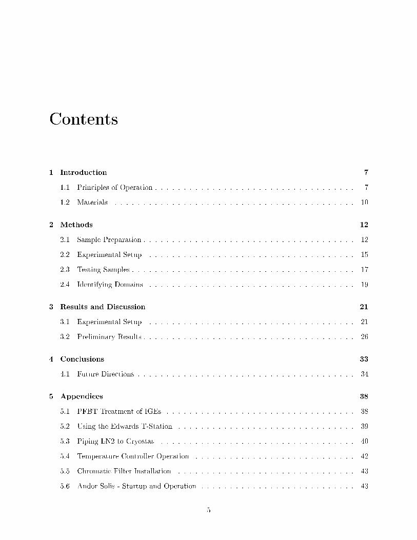
The normalized PL spectra from a donor and a D/A composite are shown in Figure 1.2. The
formation of CT excitons as well as a signi�cant quenching of the donor PL is visible in the D/A
composite. It has been found that properties of the emissive exciplex, as well as the magnitude of
donor PL quenching, provides a sensitive measure of the D/A charge transfer qualities as well as
D/A interfacial area upon acceptor domain formation [1]. The exciplex is our key to understanding
the performance of these semiconductors, as it reveals the presence of the CT exciton - potentially
the impetus of a photogenerated current.
8
1.1. PRINCIPLES OF OPERATION CHAPTER 1. INTRODUCTION
Figure 1.2: PL from Pristine ADT-TES-F and 95/5 ADT-TES-F/Pn-TIPS-F8 composite at room tem-perature. Energy level inset shows origin of peaks in PL.
In addition to electronic states, vibronic states within a semiconductor crystal are of particular
interest as they may couple to excitons and a�ect accessible excitonic energy levels. Excitonic
energy levels di�er from HOMO/LUMO levels by 0.1-0.5 eV, this energy di�erence is referred to as
the exciton binding energy. Figure 1.3 shows the e�ect of particular vibronic states (S0 and S1) on
absorption and PL spectra.
Figure 1.3: Absorption and PL of 90/10 ADT-TESF/PCBM thin �lm. S0, S1 represent the ground and�rst excited excitonic states respectively; 0,1,2: vibronic states within each level. Color-coded arrowsoverlaying the vibronic states indicate electron transitions leading to the absorption/emission peaks shown.
9

1.2. MATERIALS CHAPTER 1. INTRODUCTION
Absorption peaks at 550, 520, and 475 nm are characteristic of ADT-TES-F and its D/A compos-
ites at room temperature. Decreasing temperature in pristine ADT-TES-F �lms has been shown to
redshift absorption peaks, particularly the 0-0 peak [9]. This was attributed to enhanced Coulomb
interactions with the surrounding environment as well as exchange interactions between transla-
tionally equivalent molecules [12, 13, 14, 15].
To summarize: we aim to measure optical and photoconductive properties of our materials as
a function of temperature to establish the mechanisms of charge photogeneration, trapping and
transport. See Section 3.1 for a full description of the experimental setup implemented toward this
goal.
1.2 Materials
The materials used in these studies are derivatives of a high performance functionalized �uori-
nated anthradithiophene (ADT), ADT-triethylsilylethynyl (TES)-F, having side groups composed
of phenyl-C61-butyric acid methyl ester (PCBM) and other ADT and Pentacene (PN) derivatives
such as ADT-triisopropylsilylethynyl (TIPS-F), ADT-trisec-butylsilylethynyl (TSBS-F), Pn-TIPS-
F8, and Pn-tricyclohexylsilylethynyl (TCHS-F8). These particular acceptors were chosen for the
following reasons:
1. To separate e�ects of D/A energy o�sets from those of molecular packing on optoelectronic
properties. The HOMO/LUMO energies, as well as optical properties, of the ADT-R-F (R being
a side group) acceptors are similar to those of the ADT-TES-F donor [17], and make their D/A
LUMO o�set approximately zero. This will be contrasted with the Pn-R-F8 derivatives whose D/A
LUMO o�set is approximately 0.55 eV, an optimal value for small-molecule solar cell performance
as predicted by Monte Carlo simulations [10].
2. To study the e�ects of physical size of side groups on optoelectronic properties. ADT-TSBS-F
and Pn-TCHS-F8 R groups are considerably larger than the ADT-TIPS-F and Pn-TIPS-F8 groups.
It is expected that the D/A separation of composites containing the former will be considerably
larger than the latter. Proximity, in regards to temperature dependence, is of great importance due
to vibronic states modulating the distance between molecules.
10

1.2. MATERIALS CHAPTER 1. INTRODUCTION
Figure 1.4: Molecular structures of (top left) the donor ADT-R-F, (right side) acceptors TES, TSBS,TIPS, TCHS, and (bottom left) Pn-R-F8.[1]
Figure 1.5: aMeasured by di�erential pulse voltammetry [39,45 of JphysChem]. bMeasured in toluene.cMeasured in chlorobenzene. dMeasured in thin �lms spin-cast on PFBT treated substrates.eCalculatedfrom crystallographic data.[1]
11

2 | Methods
This section details equipment and methods implemented throughout the course of the research.
Our goal is to learn about the properties of organic semiconductors for use in optoelectronic devices.
Section 2.1 goes over how samples were made, what materials were used, and some advantages of
di�erent processes. Section 2.2 introduces important pieces of equipment and their role in the
overall experiment. Section 2.3 details the experimental methods used to determine the optical and
electronic characteristics of each sample.
2.1 Sample Preparation
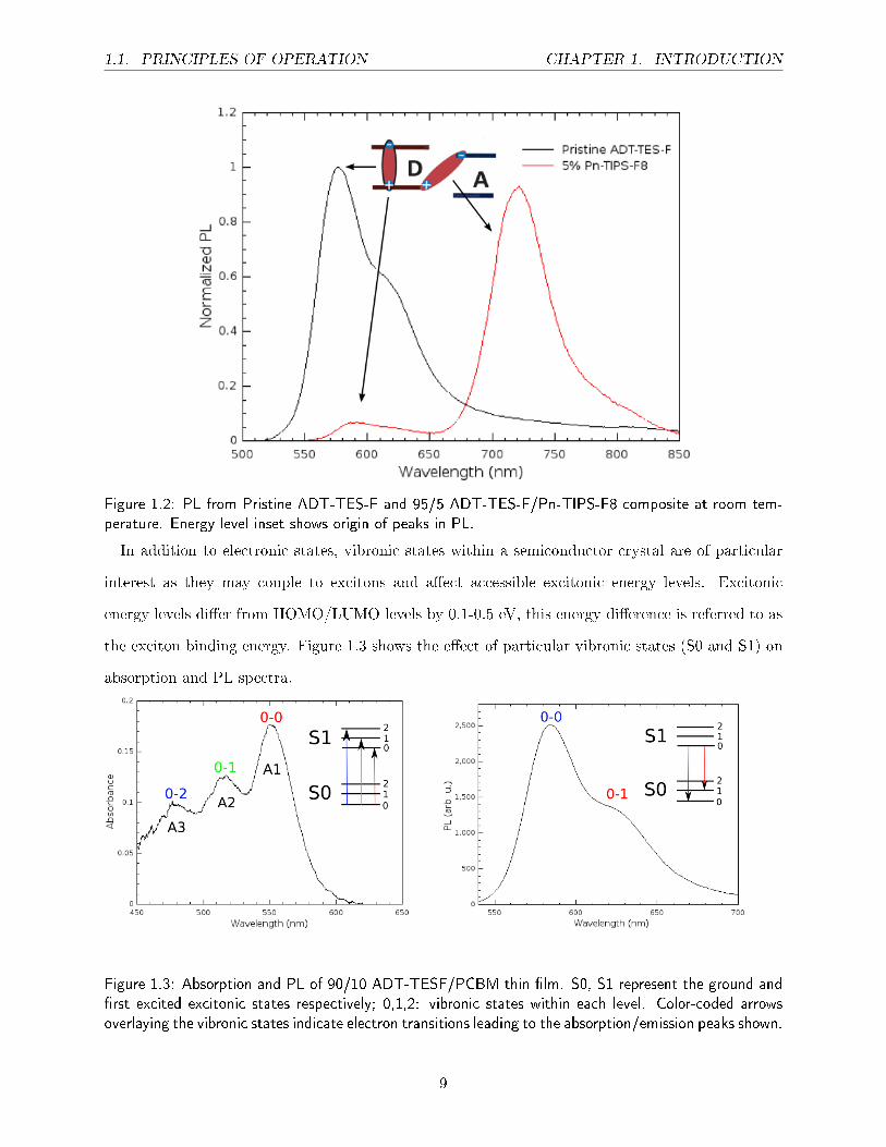
Substrates used in these experiments consist of .5mm thick quartz cover slips, and Interdigitated
Gold Electrode (IGE) pairs. IGE pairs are 5mm thick glass with photolithographically deposited 5
nm/50 nm thick Cr/Au interdigitated electrode pairs. The electrodes have ten pairs of 1-mm-long
�ngers each with a 25-µm width. Each �nger is 25-µm from the �ngers of opposite electrode. Figure
2.1 shows an IGE pair with ADT-TSBS-F crystals grown across the electrodes as well as a spincast
thin �lm on ADT-TES-F/Pn-TIPS-F8 on a quartz cover slip.
12
2.1. SAMPLE PREPARATION CHAPTER 2. METHODS
Figure 2.1: Both images taken with 10X objective. LEFT: ADT-TSBS-F crystals grown on an IGE pari,dark horizontal lines are gold electrodes. RIGHT: ADT-TESF/Pn-TIPS-F8 thin �lm on quartz cover slip.
Cover slips are cleaned by sonication in either water, ethanol, acetone or all three, and dried
using a gaseous nitrogen jet. The IGE pairs require this sonication as well as a soak in 30mM
PFBT solution. PFBT is a long chain molecule which bonds on one end to the gold electrodes,
but not to the glass. When the IGE pair is rinsed after soaking, the PFBT gets �ushed o� the
glass but remains on the gold. This PFBT is attractive to the organic molecules in this study and
allows more of them to "stick" to the gold electrodes. Practice proves that the molecules do not
only stick to the treated gold electrodes, but form bridges between them to give considerably higher
photocurrent and more consistent �lms. This exact PFBT treatment process is important to follow
precisely and is explained in detail in Appendix 5.1.
Making solutions begins with calculations. Stock solutions of donor and acceptor materials
are used to create semiconductor materials. Weight percentages were created for all samples in this
study, i.e. 90/10 ADT-TES-F/Pn-TIPS-F8 means that 90% of the total mass of semiconductor
material is ADT-TES-F and 10% is Pn-TIPS-F8.
Once calculations were performed, a Rainin SL20 2-20µL pipette was used to put correct amounts
of stock solution into a clean vial. It is important to use new, clean tips for each stock solution to
prevent contamination. The bottles are then capped, caps are secured with te�on tape, and the new
solution is sonicated for ten minutes to ensure homogeneity. Vials are labeled and the solution is
ready to be adhered to a substrate for analysis; there are two ways of carrying this out: spincasting
13

2.1. SAMPLE PREPARATION CHAPTER 2. METHODS
and dropcasting.
Dropcasting is the simpler of the two, and begins with a cleaned and prepared substrate, either
a cover slip or an IGE pair. Approximately 10µL of solution is dropped onto the substrate with a
micropipette and the solvent is allowed to evaporate, leaving only the semiconductor material on
the substrate.
This process creates �lms on the substrate, which is the desired outcome, but they are thick and
can have large amounts of self absorption (the sample absorbs some of its own emitted photons,
obscuring the nature of its electronic structure), leading to problems down the line. To remedy this,
the spincasting method is implemented, which is much more successful in creating thin, reliable
�lms.
Spincasting begins as dropcasting does, by dropping about 10µL of solution onto a clean sub-
strate. After solution is dropped onto the substrate, the substrate is placed into a Laurell spincoater
where it is suctioned onto the top of a rotating cylinder which spins at precise angular velocities
causing most of the solution to be thrown o� of the substrate. The substrate is allowed to spin long
enough for the solvent to fully evaporate - this is usually about 30 seconds.
At this point, the substrate has a thin layer of semiconductor material on it but there is one
�nal step before it is considered �nished, as IGE's are used to measure electrical properties of the
material and require clean electrical contacts to reduce noise in the signal.
IGE Prep: to create good electrical contacts on either side of the substrate the edges must be
cleared of the deposited semiconductor materials. Using lens cleaning paper soaked in cholorbenzene,
the outer sides of the IGE are wiped o�. This is a delicate process but is very doable under a 10X
microscope.
Single crystals in theory would perform exceptionally well in devices, but the manufacturing of
crystals large enough has yet to be accomplished. In the lab, however, they need not be so large and
even with their small size allow researchers to isolate mechanisms behind charge transfer, mobility,
etc., far more easily than in spincast or dropcast thin �lms. If crystal growth is required, solution
is dropped onto a substrate which is then placed in a standard freezer to slow the evaporation of
the solvent and allow larger crystals to form. Once the solvent has evaporated, the substrate is
placed under a 10X microscope and 35-40 gauge copper wire is used to transfer single cystals from
their bed on the substrate to another clean substrate for analysis. No special tools are used to
14

2.2. EXPERIMENTAL SETUP CHAPTER 2. METHODS
manipulate the copper wire, under magni�cation it is, with some concentration, manageable to use
only one's hands. It is also prudent to watch ones breathing while transferring crystals as it is easy
to accidentally blow the crystals o� the wire.
Crystals have also been grown directly onto IGE's; this is the safest and most e�ective way to
adhere crystals to a substrate. A successful example of this is shown in Figure 5.6.
Once samples have been made, they need to be tested, and for that we need a variety of experi-
mental setups. The following section details fundamental components of these setups.
2.2 Experimental Setup
Photodetectors/optical fibers are the bare bones of many of these experiments. An MPD
Avalanch photodetector as well as OceanOptics USB2000 spectrometers are implemented when
performing experiments probing optical properties of a sample. The speci�cs of these experiments
will be discussed in the Section 2.3.
Experiments which require a large number of photons to be collected, or ones in which the sample
is glowing very dimly, warrant large diameter optical �bers, around 600 µm, while experiments
which have an excess of light warrant smaller diameter �bers, around 200 µm, as not to saturate
the photodetector.
The majority of experiments incorporate a laser to excite the sample in some way. These are
either Continuous Wave (CW) or pulsed lasers:
� The 532nm CW Laser system is a Coherent Verdi-V5 laser. To preserve our samples, the
majority of these experiments will be performed with beam powers of 400 µW or less.
� The 532nm Pulsed Laser system is an Altechna MOPA-2 water cooled pulsed laser system
with a repetition rate of 50kHz.
� The 633nm Laser system is a Melles Griot HeNe Laser.
� The 355nm Laser system is a Dual Chip Nanolaser.
As We seek to gain insight into the mechanisms behind charge photogeneration, trapping and
transfer, as a function of temperature, samples are cooled to around 80K within a liquid nitrogen
fed minicryostat system.
15
2.2. EXPERIMENTAL SETUP CHAPTER 2. METHODS
The MiniCryostat, which is a Janis Research Model ST-500-UC Supertran system, is used to
perform all temperature dependent experiments. A sample is mounted inside, and the minicryostat
is evacuated by an Edwards T-Station 75 Turbo pump to approximately 10−6 Torr. It is then
cooled by supplying it with a steady �ow of liquid nitrogen - pumped into the system using gaseous
nitrogen. Note that before any liquid nitrogen is pumped through the transfer lines, these lines must
be �ushed thoroughly with gaseous nitrogen. If they are not, excess air in the lines will condense
and freeze, inhibiting the �ow of liquid nitrogen and halting the experiment.
We seek to gain, more speci�cally, an understanding of the microscopic, optoelectronic properties
of the donor, acceptor and D/A interfacial regions within a semiconductor �lm as a function of
temperature. To do this, a custom built Olympus microscope system is used.
A custom Olympus IX71 Inverted Microscope with a multitude of objectives allows us to
image these microscopic D, A, and D/A interfacial domains. The microscope has been manufactured
such that the cryostat may be mounted directly atop it, allowing us not only to observe the samples'
microscopic optical charactaristics, but also these charactaristics as a function of temperature.
Controlling the temperature during these experiments is of the utmost importance, as �uctua-
tions in temperature can give misleading data and damage the sample. To do this, a temperature
controller is used to control the internal temperature of the minicryostat.
A Lakeshore 355 Temperature controller is used to both monitor and mediate the tempera-
ture within an actively cooled cryostat. The temperature controller has three settings, low, medium
and high, for di�erent �ow rates of liquid nitrogen into the system. The controllers optimum func-
tionality is when the minicryostat is already cold (≈80K) and the �ow rate of liquid nitrogen is low.
Once the system has cooled to the minimum temperature the pressure behind the liquid nitrogen
may be taken down. The residual pressure caused by the natural warming of the liquid nitrogen
in the dewar is enough to keep the MiniCryostat cold while allowing the temperature controller to
mediate the temperature precisely.
To image these physical phenomena a high speed EMCCD camera will be implemented in con-
junction with the microscope.
The Andor Solis iXon EMCCD Camera is mounted on the side of the microscope. The
�EM� in EMCCD stands for Electron Magni�cation. The primary advantage over a standard CCD
camera is the EMCCD's negligible readout noise. The �nal crucial piece of equipment is used in all
16

2.3. TESTING SAMPLES CHAPTER 2. METHODS
electronic charactarizations of the samples.
A Keithley 237 High Voltage Source Measure Unit will be used in conjunction with IGE
pairs to learn about the electronic characteristics of the samples. The Keithley both varies voltage
to its leads and measures the current across them. It plays a crucial role in photocurrent and
transient photocurrent experiments which will be discussed in detail in the following section.
Choosing samples to continue with is the next step in the process, and to do this, we must perform
some experiments.
2.3 Testing Samples
Absorption experiments tell us about the electronic structure of the sample by showing which
wavelengths of light are absorbed. White light is shown through the sample and into a spectrometer
for analysis. As the absorption is de�ned relative to the number of photons hitting the sample, we
take a reference spectrum, having no sample material, with which to compare the transmitted light
through the sample. Calculating the absorption spectra of materials is performed with SpectraSuite
software, wherein the white light transmitted through a substrate and sample material is subtracted
from the spectrum of the white light transmitted through only the substrate. This allows for any
absorption within the substrate to be accounted for.
Continuous Wave Photoluminescence, or CW PL, tells us about the electronic energy levels
and thickness of the sample by measuring what wavelengths of light are emitted . A laser is focused
onto the sample and the emitted light is gathered by a large planar-convex lens onto an OceanOptics
USB2000 spectrometer. As the emission spectra for most of our materials lie above the wavelength
of the lasers used to excite them, we may use long pass �lters to cut the re�ection from the laser
while preserving the emission spectra. For example, taking PL with a 532nm laser, we would use a
535LP (long pass) �lter to cut out the laser re�ection from the emission spectra.
Transient Photoluminescence measures how quickly the sample responds to an incident light
pulse and how quickly the bulk of the excitons created by this incident pulse recombine. What this
experiment yields is the exciton's lifetime. Using the method outlined in Section 2.4, we may select
for either Frenkel or CT excitons. A setup similar to the CW PL is used but now with a pulsed
laser. Both 355 nm and 532 nm pulsed lasers were used in the analysis of these samples. Because
17

2.3. TESTING SAMPLES CHAPTER 2. METHODS
these pulses hit the sample at 44 kHz, and we are interested in the PL on a pulse to pulse basis,
we need to synchronize the computer with the laser output. To do this, a beam splitter is placed
in the path of the pulsed laser and a portion of the laser is re�ected onto a photodetector. This
photodetector is not the same as the spectrometer collecting light from the sample; it is used only
to synchronize the computer with the laser. When each pulse hits the photodetector, the change in
voltage is sent to the computer, allowing us to know when the laser is emitting. Once the computer
is synched with the laser output, we look at the emitted light in the unit of time between each
pulse. Each pulse is equally spaced, and because the amount of light emitted between each pulse
is very small, the software sums each emission spectra from each unit of time between pulses, on
one screen; this gives us approximately a 35µs range between pulses to observe the �ne, emmissive
properties of the sample, as a function of time, after a laser pulse is incident upon it.
One goal of this research is to learn about the properties of organic semiconductors for use in
electronic devices; the next few experiments focus on the electronic and optoelectronic properties
of the samples.
Continuous Wave Photocurrent, or CW Photocurrent, is conducted on an IGE pair using
a Keithley Source Measure Unit that simultaneously varies the voltage and measures the current
over its leads. A sample is prepared (usually spincast solution on an IGE pair) and leads from
the Keithley are placed on the outer conducting contacts of the IGE pairs. It is crucial that these
contacts be clean to eliminate noise. Exciting the sample and varying the voltage from low (0V) to
high (around 150V), we observe the relation between the current response and voltage applied. To
separate the current due to the voltage applied through the semiconductor material from that due
to photogenerated charge carriers, a �dark� current measurement is taken �rst. The voltage is varied
from low to high while the sample is not being hit with the laser, and the current is recorded. It is
expected that the current is higher in the samples undergoing excitation as this generates excitons
which, due to the voltage applied, are likely to dissociate and create free charge carriers.
Another factor in understanding the performance of a sample is how fast the current responds
to an incident optical pulse. This reaction time is explored in an experiment called the transient
photocurrent.
Transient Photocurrent works on similar principles to the CW photocurrent, but instead of
a continuous wave laser, a pulsed laser is used. Using a Tektronix Communication Signal Analyzer
18

2.4. IDENTIFYING DOMAINS CHAPTER 2. METHODS
(CSA) 8200 allows us to measure input signals of very high frequencies, up to 50 GHz. We are
looking for the time it takes to generate photocurrent within the sample after the sample is excited.
It is necessary to synchronize the laser pulses with the software on the oscilloscope, so that the
oscilloscope is looking in the region between pulses. This is done by using a photodetector in
the same way as described in the transient PL. The intensity of the synching signal is incredibly
important in this experiment as it could damage the CSA if it is too large. To tune the strength
of the input signal, we vary the amount of light hitting the photodetector either by adjusting the
beam splitter's angle or moving the photodetector so that a smaller portion of the laser is incident
upon it. Important things to note before beginning the experiment:
· Any operator of the CSA needs to be grounded using either the grounding wristband connected
to the CSA (recommended) or by touching the optical bench before any contact with the CSA. The
CSA is very sensitive and any static discharge could damage its components.
· The input synching signal needs to be between -800mV and -2000mV, if it is outside this range
it could damage the CSA. To test this, �rst measure the synch signal on the 300MHz Agilent
DSO6032A oscilloscope. Then, when it is in the appropriate range, make sure you are grounded
and connect the synch signal to the CSA.
· Although the CSA is a touch screen machine, it is best and safest to use the keyboard and
mouse. Windows 2000 is installed on it.
· To save data on an external drive, USB ports are connected externally via a large USB dock.
Two measurement durations may be taken during the transient photocurrent experiments: short
and long. The short duration looks closer to the initial pulse (< 5 ns) and allows us to see more
clearly how the photocurrent rises after being hit by a laser pulse. The longer duration stretches
further from the initial pulse (> 20 ns) and allows us to see how long it takes the photocurrent to
fall to 1e of its maximum value once the pulse has been turned o�. Both are important pieces of
information and help with understanding the optoelectronic properties of the sample.
2.4 Identifying Domains
Spatial isolation of speci�c regions within an organic semiconductor material amounts to �ltering
out all the light except that indicative of the region of interest. To do this, Chroma chromatic
19

2.4. IDENTIFYING DOMAINS CHAPTER 2. METHODS
�lters were used. See Appendix 5.5 for explicit installation instructions. To isolate donor emission,
540LP(long pass) and 640SP(short pass) �lters are used. Similarly, to isolate regions of exciplex
formation, a 680LP �lter was used. The idea is shown in Figure 2.2.
Figure 2.2: 95/5 ADT-TES-F/Pn-TIPS-F8 composite PL overlaid with dark regions to demonstratewavelengths being �ltered out. Left: a 540LP and 640SP combine to allow only the donor emission tobe imaged. Right: a 680LP �lter removes the donor emission and allows for all the exciplex emission topass.
20

3 | Results and Discussion
3.1 Experimental Setup
A main goal of this project was the construction of an experimental setup to enable low temperature,
microscopic measurements of both optical and electronic propeties of our materials. The �rst step
toward this was the minicryostat, which provided the potential for a high vacuum (10−6 Torr)
environment to minimize oxidation and photobleaching during photoexcitation.
To achieve that high vacuum environment, an Edwards T-Station 75 Turbo Pump was �tted to
the cryostat. The �rst vacuum test, achieving an internal pressure of 1.2x10⁻⁶ Torr, con�rmed that
the turbo pump was working correctly and that the cryostat was well sealed. Measurement of the
exact pressure required the purchase of an external attachment for the turbo pump which connected
via USB to the turbo pump's computer. See Appendix 5.2 for particular information on operating
the Edwards T-Station 75.
Once the cryostat-turbo pump system was con�rmed to achieve a high vacuum, we needed a way
to cool the sample inside to temperatures of ≈ 80K. With the cryostat system came an insulated
and pre-evacuated transfer line capable of carrying liquid nitrogen (LN2). It is important that the
vacuum in the transfer line be very high, as any absorbed heat will reduce the lines e�ciency and
require the use of more LN2 to cool the sample. The line has two legs, one on each end, and one
that �ts into an inlet leg on the cryostat. Inserting one end of the line into a 25 L insulated dewar
and the other into the cryostats inlet leg allowed for the transfer of LN2 to the cryostat's sample
holer. A source of gaseous nitrogen was used to pressurize the dewar and force the LN2 into the
cryostat. See Appendix 5.3 for diagrams and instructions on exact procedures.
The most crucial step in the cooling procedure is the measurement and control of the cryostat's
21

3.1. EXPERIMENTAL SETUP CHAPTER 3. RESULTS AND DISCUSSION
internal temperature. To do this, a Lakeshore 355 Temperature Controller was used. The tempera-
ture controller performs two tasks: 1. report the internal temperature to ±0.01 K by communicating
with a pre-installed thermister on the cryostat's sample mount, and 2. control the internal temper-
ature by supplying current to a heating coil which is in thermal contact with the cryostat's sample
mount. See Appendix 5.4 for detailed temperature controller operation instructions.
Using the temperature controller in conjunction with the turbo pump and LN2 transfer line,
temperatures of 78K were consistently achieved in ≈15 minutes, stabilizing to ±0.01 K of the desired
temperature after another 10 minutes. It is important to note that whenever conducting temperature
dependent experiments, the cryostat will reach the desired temperature and then overshoot it.
After 10 minutes of oscillation the temperature will be nearly time invariant and experiments may
commence.
Once a high vacuum environment with controllable temperature had been constructed, the
microscopic optical and electronic measurement capabilities had to be built in. With imaging
being the initial purpose of the cryostat, it was pre-ordered with �ttings that matched the trans-
lational stage atop the Olympus IX71 inverted microscope. Installing the cryostat con�rmed that
the mount worked, and that the entire system may be translated atop the microscope.
The next step was to design a sample holder. The sample holder needed to �t inside the cryostat
chamber while handling optical and electronic measurements in parallel. Electronic measurements
need to be performed under back illumination to minimize the e�ect of self absorbance within
the sample. Another hurdle to performing microscopy within the cryostat is placing the sample
within the working distance of the microscope objective without breaking the thin quartz window;
the sample holder therefore needed to have some vertically translational ability to compensate for
varying working distances of the lenses. As the cryostat needs to undergo signi�cant rotation and
motion to be installed on the microscope, the sample holder also needed a �rm grip on the sample
as to keep it from falling during installation. Figure 3.1 details the sample holder created to satisfy
these conditions.
22

3.1. EXPERIMENTAL SETUP CHAPTER 3. RESULTS AND DISCUSSION
Figure 3.1: Sample holder for electrical measurements or back illuminated PL in the minicryostat. Thesample may be translated 5 mm toward or away from the lower quartz window to accomodate varyingobjective working distances. Components shown are the following: 1. Substrate. 2. IGE. 3. Goldradiation shielding. 4. Microscope objective. 5. Quartz windows. 6. Gold leads to IGE. 7. Coppermount. 8. Sample holder base. 9. To Keithley Source Measure Unit. 10. Exterior walls of the cryostat.
To ensure the sample holder worked as advertised, a 98/2 ADT-TES-F/PCBM was mounted
into the sample holder, and the sample holder installed in the cryostat. After pumping down to
10−6 Torr, the dark current was taken. Pumping down was performed less for the protection of
the sample, as it was not being excited, and more to test that the sample holder maintains good
contacts. The turbo pump begins operation by using a roughing pump to remove a good portion of
the air before the turbo turns on. This roughing pump sends vibrations to the cryostat and sample
holder that may shake the leads loose. If the sample holder maintains good contact we expect to see
a linear increase in current with voltage. Figure 3.2 con�rms that this sample holder is maintaining
good contact with the IGE pairs through pumping down, and may be used for further electronic
and optical measurements within the cryostat.
23

3.1. EXPERIMENTAL SETUP CHAPTER 3. RESULTS AND DISCUSSION
Figure 3.2: 98/2 ADT-TES-F/PCBM dark current taken inside the minicryostat at 10−6 Torr.
As described in Section 2.4, domains of speci�c D, A, and D/A interfacial regions emit di�erent
PL spectrums in response to photoexcitation. To capture these varying responses, we �rst needed
to capture their image. Onto one of the microscopes' ports, we attached an Andor Solis IXON
EMCCD camera which is sensitive to all wavelengths of interest to us - speci�cally about 500-1000
nm. For speci�cs on startup and operation, see Appendix 5.6. After installing the appropriate
�lters into the microscope, imaging may take place. To test the setup, we used a spincast thin �lm
of 80/20 ADT-TES-F/Pn-TIPS-F8. The composite yielded images, shown in Figure 3.3, having
the expected properties; speci�cally that the exciplex emission was of a greater intensity than the
donor emission - as predicted by bulk PL measurements (Figure 1.2, 2.2).
24

3.1. EXPERIMENTAL SETUP CHAPTER 3. RESULTS AND DISCUSSION
Figure 3.3: 80/20 ADT-TES-F/Pn-TIPS-F8 images under 60X magni�cation: Left - 540SP and 640LP�lter to isolate donor domains, Right - 680LP �lter to isolate exciplex formation.
Temperature dependent measurements were the next step in the process. As the temperature
controller, LN2, turbo pump, and optical measurement capability had already been established,
taking temperature dependent optical measurements became a matter of getting it all to work
together. The sample chosen was a single crystal of ADT-TES-F grown and transplanted onto
a glass cover slip substrate as described in Section 2.1. The cryostat was evacuated to 1.3x10⁻⁶
Torr, the sample cooled to 78K, and the temp increased by 10K increments via the temperature
controller. Figure 3.9 details the PL obtained. This result con�rmed that temperature dependent
measurements were possible and produced consistent results. The �nal experimental setup for low
temperature optical and electronic study of our organic semiconductor materials is shown in Figure
3.4.
25

3.2. PRELIMINARY RESULTS CHAPTER 3. RESULTS AND DISCUSSION
Figure 3.4: MiniCryostat mounted atop the Olympus inverted microscope. In this diagram, the sampleis inside the MiniCryostat and its optical image is shown on the computer. This image was a 95/5ADT-TES-F/IF-MES sample spincast onto an IGE pair taken with a 100X objective.
To recapitulate, we have designed, built and tested an experimental setup to perform low tem-
perature microscopy as well as electronic measurements within the minicryostat. The sample holder
maintains good electrical contact through the operation of the roughing pump while allowing us the
vertically translational freedom to place the sample within the working distance of our objectives.
This has yielded images that, making use of chromatic �lters, show distinct regions of donor and
donor-acceptor PL, opening the door for the spatial isolation of D, A, and D/A interfacial domain
formation and observation of domain speci�c charge carrier and exciton dynamics.
3.2 Preliminary Results
Preliminary results on our materials have also been gathered, the �rst of which is absorption, shown
in Figure 3.5. While the absorption was not taken in the experimental setup described in Figure
3.4, it allows us to gain information about excitonic energy levels within the materials.
26
3.2. PRELIMINARY RESULTS CHAPTER 3. RESULTS AND DISCUSSION
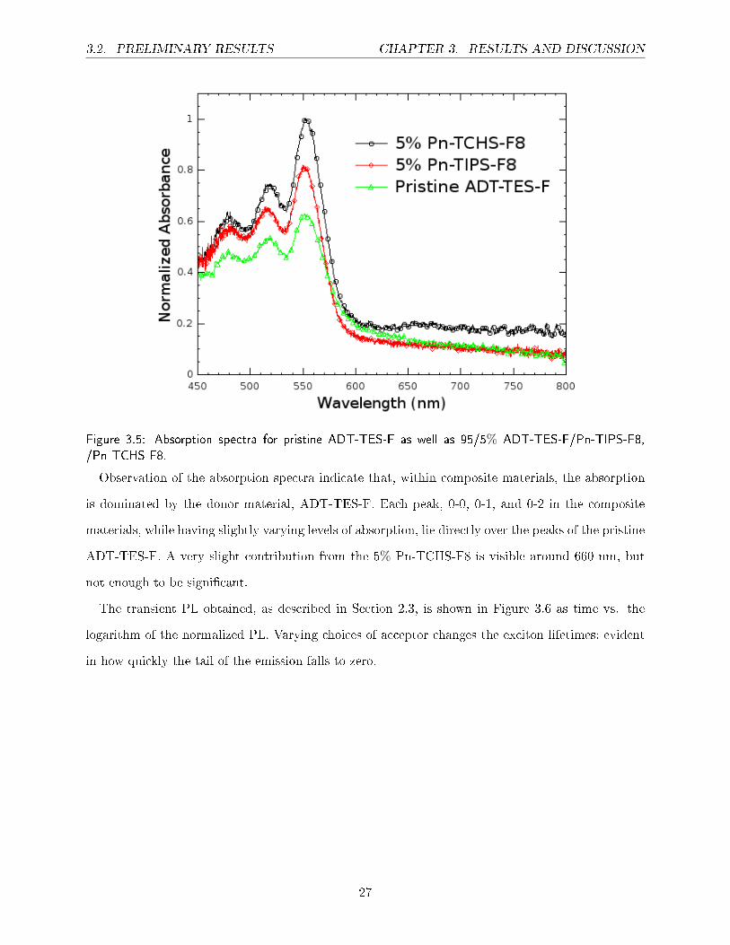
Figure 3.5: Absorption spectra for pristine ADT-TES-F as well as 95/5% ADT-TES-F/Pn-TIPS-F8,/Pn-TCHS-F8.
Observation of the absorption spectra indicate that, within composite materials, the absorption
is dominated by the donor material, ADT-TES-F. Each peak, 0-0, 0-1, and 0-2 in the composite
materials, while having slightly varying levels of absorption, lie directly over the peaks of the pristine
ADT-TES-F. A very slight contribution from the 5% Pn-TCHS-F8 is visible around 660 nm, but
not enough to be signi�cant.
The transient PL obtained, as described in Section 2.3, is shown in Figure 3.6 as time vs. the
logarithm of the normalized PL. Varying choices of acceptor changes the exciton lifetimes; evident
in how quickly the tail of the emission falls to zero.
27

3.2. PRELIMINARY RESULTS CHAPTER 3. RESULTS AND DISCUSSION
Figure 3.6: Bulk transient PL of exciplex emission in ADT-TES-F/Pn-TIPS-F8 and ADT-TES-F/Pn-TCHS-F8 composites.
D/A composites with Pn-TCHS-F8 as the acceptor have shown shorter exciplex lifetimes than
those with Pn-TIPS-F8 as the acceptor. This could be due to the large intermolecular spacing
induced by the physical size of the TCHS molecule, as described in Section 2.1. The charges in
the CT exciton between ADT-TES-F and Pn-TIPS-F8 are so far apart that a large number of
them dissociate, e�ectively shortening the exciplex's lifetime. The corollary of this is the relatively
long lifetimes of excitons in D/A composites with Pn-TIPS-F8 as the acceptor. The e�ect of
intermolecular spacing due to varying side groups on the donor shows itself in the bulk PL of D/A
composites as well, and is shown in Figure 3.8.
Around the beginning of these experiments, our 532 nm Altechna pulsed laser, used in transient
photocurrent experiments, was sent away for repairs and has not yet returned. Previous studies,
however, of the transient photocurrent in our materials have been conducted. The paper "Temper-
ature dependence of exciton and charge carrier dynamics in organic thin �lms" by A.D. Platt et. al,
observed an increase in the photocurrent from pristine ADT-TES-F with increasing temperature.
Figure 3.7 shows photocurrent transients obtained under 355 nm, 500 ps excitation. The inset shows
normalized photocurrent transients at 298 and 98 K.
28

3.2. PRELIMINARY RESULTS CHAPTER 3. RESULTS AND DISCUSSION
Figure 3.7: Transient photocurrent obtained under 355 nm 500 ps photoexcitation of a pristine ADT-TES-F �lm at 1.2x10⁵ V/cm, at various temperatures. [9]
As temperature decreased, two main changes were observed: 1. the main peak decreased, and 2.
the initial decay dynamics became faster and more pronounced [9].
The inset shows the second change mentioned and is evidence for thermally activated hole hopping.
As the temperature decreases there is less thermal energy in the material to allow the hole to "hop"
out of a trap. The transient photocurrent is gathered well before excitons may form, and is a
product of fast photocurrent dynamics. See [16] for a model that describes nanosecond time-scale
photocurrent dynamics in (ADT) �lms and ADT-based D/A composites.
PL, as well as imaging, of several D/A composites have been performed in the experimental
setup detailed in Figure 3.4. The PL shown in Figure 3.8 shows evidence of the spatial separation
of D/A molecules a�ecting CT exciton dynamics. Exciplex peaks observed are in agreement with
the predicted di�erence in energy between the LUMO of the donor and HOMO of the acceptor, ≈
715-720 nm..
29
3.2. PRELIMINARY RESULTS CHAPTER 3. RESULTS AND DISCUSSION
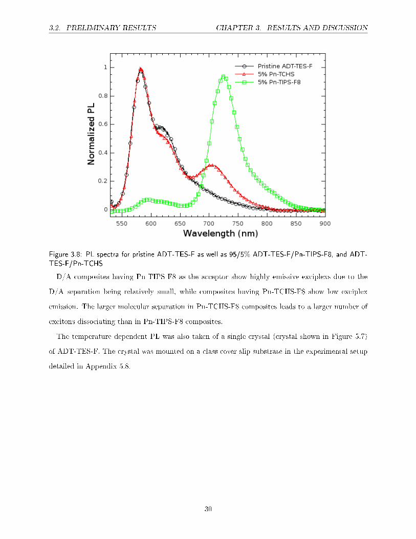
Figure 3.8: PL spectra for pristine ADT-TES-F as well as 95/5% ADT-TES-F/Pn-TIPS-F8, and ADT-TES-F/Pn-TCHS
D/A composites having Pn-TIPS-F8 as the acceptor show highly emissive exciplexs due to the
D/A separation being relatively small, while composites having Pn-TCHS-F8 show low exciplex
emission. The larger molecular separation in Pn-TCHS-F8 composites leads to a larger number of
excitons dissociating than in Pn-TIPS-F8 composites.
The temperature dependent PL was also taken of a single crystal (crystal shown in Figure 5.7)
of ADT-TES-F. The crystal was mounted on a class cover slip substrate in the experimental setup
detailed in Appendix 5.8.
30

3.2. PRELIMINARY RESULTS CHAPTER 3. RESULTS AND DISCUSSION
Figure 3.9: Temperare dependent PL of single crystal ADT-TES-F taken within the cryostat. Downwardpointing arrow indicates increasing temperature.
Decreasing temperature led to increasing PL counts in the single crystal. As vibrational modes
were frozen out of the crystal, less excitons could recombine non-radiatively into phonons, leading
to more radiative recombination and higher PL counts.
One of the most exciting functionalities of this setup is its ability to image microscopic D/A
domains. Using chromatic �lters and the Andor Solis IXON EMCCD as described in Section 2.4,
we may spatially isolate regions of the semiconductor by isolating their emission.
Figure 3.10: ADT-TES-F/Pn-TIPS-F8 composites excited at 532 nm under 60X magni�cation. Outlinedis a region of ADT-TES-F donor material. Left: 680LP �lter shows regions of exciplex formation betweendonor and acceptor molecules; arrows point to regions of exciplex emission surrounding the donor material.Right: 540LP and 640SP show regions where Frenkel excitons are recombining, indicating the presenceof ADT-TES-F.
31

3.2. PRELIMINARY RESULTS CHAPTER 3. RESULTS AND DISCUSSION
Exciplex emission is seen outlining donor regions shown in the left side image. These emissions
indicate charge transfer states existing at the grain boundary between donor and acceptor molecules.
This image is showing explicitly where donor and D/A interfacial regions exist, and con�rms that
D/A interfacial regions, and thus CT states, exist at the grain boundaries between donor domains.
32

4 | Conclusions
Elucidating the temperature dependence of our organic semiconductors may allow us to isolate the
speci�c mechanisms of charge photogeneration, transport, and trapping. While we have gleaned
important insight into these materials through bulk studies, microscopic studies had not yet been
performed and would allow for a much higher level of control over which exact domain within a
composite is being excited, as well as which domain is being observed. This level of control could
lead to much more direct experimental data on Frenkel and CT exciton dynamics.
In pursuit of temperature dependent microscopic, optical and electronic measurements, an experi-
mental setup was constructed. This setup needed to support optical and electronic measurements in
parallel while not destroying the sample. The setup described in Figure 3.4 was built and tested. In-
ternal pressures within the minicryostat of 10−6 Torr were achieved, ensuring that the sample would
not undergo oxidation and be damaged during optical measurements. The cryostat was also tested
to achieve temperatures of 78K consistently, and in conjuction with the Lakeshore temperature
controller, the temperature was controllable to ±0.01K in the range above that.
To perform microscopic measurements, an Olympus inverted microscope was implemented be-
neath a translational stage. The translational stage allowed for more precise maneuvering of the
cryostat and thus the sample, within the image plane. Before images were taken, however, we
needed a way to place the sample within the working distance of the particular objective in use.
We also needed to be able to perform electronic measurements while inside the cryostat, and to
backlight these experiments as to minimize the e�ect of self absorption within the sample. A third
condition on the sample holder was that it needed to hold the sample �rmly to keep it from falling
during the cryostat installation procedure, and during the pumping down process. The sample
holder designed satis�ed this vertically translational requirement to accomodate varying working
33

4.1. FUTURE DIRECTIONS CHAPTER 4. CONCLUSIONS
distances, supported backlighting for electronic measurements, held the sample tightly and �nally
was tested and showed good electrical contacts with an IGE sample post pump down. The sample
holder is shown in Figure 3.1.
After the experimental setup was con�rmed to be operational, some preliminary results on our
samples were obtained. Donor dominated absorption was observed in our materials. PL measure-
ments of ADT-TES-F composites showed a decreased exciplex emission as the spatial separation of
the molecules increased. Larger inter-molecular spacing also led to shorter exciplex lifetimes. This
is consistent with previous results [1].
Temperature dependent studies revealed that thermally activated hopping was decreased as tem-
perature decreased. This led to a decrease in charge hopping and thus a decrease in photocurrent.
Isolating speci�c donor and D/A interfacial domains was the �nal result obtained. Exciting a
sample of ADT-TES-F/Pn-TIPS-F8 at 532 nm under 60X magni�cation, and using chromatic �lters,
as described in Section 2.4, yielded images showing explicit donor and D/A interfacial domains.
Figure 3.10 shows these images. D/A interfacial regions are seen outlining larger donor domains.
This result showcased that it is now possible to image individual domains within a spincast D/A
composite material, and to study speci�c exciton and charge carrier dynamics within and around
these domains.
4.1 Future Directions
The result in Figure 3.10 is an exciting one as it allows for the isolation of D, A, and D/A interfacial
domains. Using a di�raction limited beam spot, we plan to translate the spot across a donor
region and explore optical and electronic properties as a function of distance into the domain. This
will illuminate speci�c exciton di�usion lengths at speci�c temperatures. If, for example, we are
translating the beam spot from the center of a donor domain to the edge, and when the beam
spot is 5 µm from the interfacial region we begin to see exciplex emission, then we will know that
the Frenkel excitons are di�using at least 5 µm to create CT states and emissive exciplexes at the
boundary. We may also perform this experiment as a function of temperature, to quantify how far
the excitons will di�use when we freeze out vibrational modes in the organic semiconductor.
Another potential is to study microscopic emission in D/A thin �lms dependent on excitation
34

4.1. FUTURE DIRECTIONS CHAPTER 4. CONCLUSIONS
polarization. Molecules aligned with the polarization direction should absorb, and then re-emit, the
light more e�ciently - similarly to a polarizer. By varying the polarization of the incident light,
we may determine speci�c grain orientations within a particular domain. Preliminary studies have
already been conducted and show promising results. Figure 4.1 shows a thin �lm of pristine ADT-
TES-F excited with 532 nm laser light at polarization angles of 0o and 90o. The speci�c polarization
angles of the incident light in these images are arbitrary, but it is clear that orthogonal polarizations
cause complementary areas of the semiconductor to �uoresce.
Figure 4.1: Pristine ADT-TES-F excited at 532 nm under 60X magni�cation. Left: Polarization angleof incoming light is 0o. Right: polarization of incoming light is 90o
While in its early stages, this may be able to tell us considerable amounts about how these semi-
conductors form, what orientations they prefer, and what orientations lead to desirable properties.
This could allow us to tune acceptors and acceptor concentrations for optimal performance, as well
as further isolate mechanisms behind charge photogeneration, transport, and trapping.
35

Bibliography
[1] Paudel, K., B. Johnson, A. Neunzert, M. Thieme, B. Purushothaman, M. M. Payne, J. E.
Anthony, and O. Ostroverkhova. "Small-Molecule Bulk Heterojunctions: Distinguishing Between
E�ects of Energy O�sets and Molecular Packing on Optoelectronic Properties." The Journal of
Physical Chemistry C 117.47 (2013): 24752-4760. Print.
[2] Heeger, A. J. Chem. Soc. Rev. 2010, 39, 2354�2371.
[3] Ostroverkhova, O., Ed. Handbook of Organic Materials for Optical and (Opto)Electronic De-
vices, 1st ed.; Woodhead Publishing Limited:
Cambridge, U.K., 2013.
[4] Samuel, I. D. W.; Turnbull, G. A. Chem. Rev. 2007, 107, 1272-1295.
[5] Katz, H. E.; Huang, J. Annu. Rev. Mater. Res. 2009, 39, 71-92.
[6] Yeh, N.; Yeh, P. Renewable Sustainable Energy Rev. 2013, 21,
421-431.
[7] Ostroverkhova, O.; Moerner, W. E. Chem. Rev. 2004, 104, 3267-
3314.
[8] Facchetti, A. Chem. Mater. 2011, 23, 733-758.
[9] Platt, A., M. Kendrick, M. Loth, J. Anthony, and O. Ostroverkhova. "Temperature Dependence
of Exciton and Charge Carrier Dynamics in Organic Thin Films." Physical Review B 84.23
(2011): n. pag. Print.
36

BIBLIOGRAPHY BIBLIOGRAPHY
[10] Peumans, P.; Forrest, S. R. Chem. Phys. Lett. 2004, 398, 27-31.
[11] A. D. Platt, J. Day, S. Subramanian, J. E. Anthony, and
O. Ostroverkhova,J. Phys. Chem. C113, 14006 (2009).
[12] O. Ostroverkhova, S. Shcherbyna, D. G. Cooke, R. F. Egerton, F. A.
Hegmann, R. R. Tykwinski, S. R. Parkin, and J. E. Anthony,J. Appl.
Phys. 98, 033701 (2005). 28
[13] F.C. Spano,J. Chem. Phys. 122, 234701 (2005). 29
[14] F.C. Spano, Acc. Chem. Res. 43, 429 (2010). 30
[15] F. C. Spano, J. Clark, C. Silva, and R. H. Friend, J. Chem. Phys.
130, 074904 (2009).
[16] Johnson, Brian, Mark J. Kendrick, and Oksana Ostroverkhova. "Charge Carrier Dynamics in
Organic Semiconductors and Their Donor-acceptor Composites: Numerical Modeling of Time-
resolved Photocurrent." Journal of Applied Physics 114.9 (2013): 094508. Print.
[17] Platt, A. D.; Day, J.; Subramanian, S.; Anthony, J. E.;
Ostroverkhova, O. J. Phys. Chem. C 2009, 113, 14006-14014.
37

5 | Appendices
5.1 PFBT Treatment of IGEs
To create a PFBT monolayer on an IGE substrate:
1. Clean the substrate with DI water
2. Dip the substrate in a clean bottle of isopropyl alcohol (IPA)
3. Sonicate the substrate, using the Branson 1510 Sonicator, in IPA for 5 minutes
4. Remove the substrate from IPA and place into clean bottle of Acetone
5. Sonicate the substrate for 5 minutes in Acetone
6. Remove substrate and clean with DI water
7. Make new PFBT solution everytime. PFBT solution goes bad within a few days
8. To make 30 mM PFBT solution, mix 16 µL PFBT in 4 mL ethanol (or ethyl alcohol)
9. Once the solution is made, place the substrate in a clean bottle and pour the 30 mM PFBT
solution over it. Note: it is best to use as small a bottle as possible and preferably one with
a lid to prevent evaporation of the 30 mM PFBT solution during the soaking process.
10. Let the substrate sit in the solution for 30 minutes. This timing is important so be sure to
use a timer.
11. After 30 minutes, remove the substrate and rinse with ethanol.
12. Sonicate in ethanol for �ve minutes.
38

5.2. USING THE EDWARDS T-STATION CHAPTER 5. APPENDICES
13. Remove from ethanol and dry with the N2 jet.
The substrate has now been PFBT treated. PFBT has two distinct ends, one of which has been
found to attract and bind with organic semiconductor molecules while not in�uencing their optical
or electronic characteristics. The other end binds with the gold and not the glass. This causes the
organic materials to conglomerate around the IGEs and initiates crystal growth spanning the gold
electrodes.
5.2 Using the Edwards T-Station
Before turning on the turbo pump be sure that all joints leading to the cryostat are sealed tightly
and that the valve connecting the cryostat and the turbo pump is open. If any joints are left loose
or open the roughing pump could be damaged. To turn on the pump:
1. Plug it in. The plug is near the back of the pump. When the machine is plugged in, the lights
on the display should come on.
2. When you have made sure all the seals leading to the cryostat are tight, press the leftmost
button with the diamond on it. This starts the roughing pump. The numbers on the display
will show 0 and there will be a % sign �ashing to the right. The numbers will stay zero until
the turbo pump is engaged - 120 seconds after the roughing pump has been initialized. The
numbers indicate the percent of full speed that the turbo pump is currently spinning. When
the turbo pump has reached maximum speed, the % sign will stop �ashing.
3. To view the current pressure within the pump, press the rightmost button with the rightfacing
arrow on it. Keep pressing it until the light next to GAUGE comes on. The display will then
read a pressure in Torr.
4. To turn o� the pump, �rst press the leftmost button with the diamond on it, then press the
center button with the bent arrow. The pump will then begin to deccellerate.
It is important not to bump or move the pump while it is operating as it could damage the high
speed parts. Make sure it is tucked under the optical bench or otherwise away from stray feet. As
39

5.3. PIPING LN2 TO CRYOSTAT CHAPTER 5. APPENDICES
many of these experiments are performed in the dark, it is generally a good rule to keep �oorspace
clear.
5.3 Piping LN2 to Cryostat
Before cooling down:
� It is important that the cryostat be prepared to cool down when the cooling starts. This
means that it is evacuated down to ≈ 10−6 Torr and the sample is prepared inside it.
� Care should be taken not to bend the transfer line to a radius of less than 12 inches, to prevent
possible damage to the inner line.
One leg at the end of the transfer line should be longer than the other - this is the storage dewar
leg, as shown in Figure 6.1 and 6.4, that goes into the LN2. Insert this through the lid of the dewar,
shown in Figure 6.4, and into the dewar. Make sure it is supported as it stands (bungee cords
normally work well for this). The lid of the dewar is secured with C-clamps and zip ties, as shown
in Figure 6.4.
Figure 5.1: Transfer line to connect LN2 to cryostat.
The cryostat leg of the transfer line slides easily into the inlet leg of the cryostat, shown in Figure
6.2. To tighten the cryostat leg into the inlet leg, twist the gold tightener on the end of the inlet leg.
When the dewar lid is tightened on, we may begin pressurization. It is important to note, however,
that before this happens the �ow regulator valve of the transfer line must be opened at least 3-5
full turns to allow LN2 to �ow through.
40

5.3. PIPING LN2 TO CRYOSTAT CHAPTER 5. APPENDICES
Figure 5.2: Janis Research Model ST-500-UC Supertran Minicryostat.
Connect the gaseous nitrogen hose to the dewar lid and tighten �rmly. Turn the gaseous nitrogen
valve on, shown in Figure 6.3, until you hear gas �owing. The pressure gauge on the dewar lid
should begin to rise, once it reaches 3.5-4 PSI, turn down the gaseous nitrogen �ow. Optimal
pressure within the dewar for pumping LN2 is about 5 PSI. The safety valve, shown in Figure 6.3,
will not allow the pressure within the dewar to exceed ≈8 PSI. Expect to wait 3-4 minutes before
any signi�cant cooling of the sample begins.
Figure 5.3: Equipment to supply gaseous nitrogen to the LN2 dewar for pressurization.
41

5.4. TEMPERATURE CONTROLLER OPERATION CHAPTER 5. APPENDICES
Figure 5.4: Dewar with gaseous nitrogen hose and dewar leg of transfer line attached.
While the LN2 is �owing, make sure that the exhaust leg on the cryostat is clear of any optics
and not dripping liquid. If it is dripping, decrease the pressure in the dewar.
5.4 Temperature Controller Operation
To operate the temperture controller:
1. Turn the machine on via the switch on the back.
2. To set the desired temperature, click "Set Point", enter the desired temperature in Kelvin,
then hit enter.
3. There are three heater settings: Low, Med, High. For high precision temperature control,
use the Low setting. For large temperature changes which require low precision, use the High
setting.
Remember, the temperature controller can only increase the temperature of the sample. Main-
taining the temperature in the cryostat is a delicate art in balancing the �ow of LN2 with the heat
supplied by the temperature controller.
42

5.5. CHROMATIC FILTER INSTALLATION CHAPTER 5. APPENDICES
5.5 Chromatic Filter Installation
Installing chromatic �lters into the Olympus IX71 Inverted microscope is very straightforward. On
the right side of the microscope, just beneath the shutter switch, there is a small hole. Use the
allen wrench on the back of the microscope to loosen the bolt in the hole. Once the bolt is loosened
(it doesnt need to come out, just be loose) the entire cassete may be slid out the left side of the
microscope.
Figure 5.5: Right side of microscope indicating the casette containing 6 chromatic �lter holders as wellas the small hole to loosen the bolt holding the casette.
To insert �lters, rotate the wheel around until the desired location is reached, and use the same
allen wrench to loosen the bolt atop the �lter mount. This too only needs to be loose to remove.
Unscrew the top of the �lter mount and gently place the �lter into the mount. Screw the top of the
mount back on, tighten the mount back in its place in the casette, and insert the casette back into
the microscope. Use the same allen wrench to re-tighten the casette onto the microscope and it is
ready to use.
5.6 Andor Solis - Startup and Operation
Before operating the Andor Solis IXON EMCCD camera make sure that the shutter leading to
the camera is CLOSED. If the CCD array in the camera is hit with light and is not yet cooled to
operating temperature, the array could be damaged.
To initiate the Andor Solis IXON EMCCD camera:
43
5.7. SINGLE CRYSTAL NOTES CHAPTER 5. APPENDICES
1. Plug it in. There are two plugs at the rear of the camera: one power and one to communicate
with the computer. Plugging these in should start the fan within the camera. This fan is used
to cool the CCD array.
2. To open the software, click the Andor icon on the desktop.
3. Once the software opens, the camera should begin to cool to the preset temperature. There is
a red box in the bottom left of the window with the current temperature. If the temperature
is not decreasing, click "Hardware", then Temperature, and check that the temperature is set
to -60 C and that the cooling is turned on.
4. To view a real time video, click the icon with the video camera on it. A window will pop up
with the video showing.
5. To take a snapshot of the video shown, click the "Take Signal" button with the �lm camera
on it and the frame will freeze. The frame will then be frozen and able to be saved.
Note: the camera is only rated to cool to -60o C with air cooling. This is plenty cold and works
very well. If the temperature setting in the software is set to lower than that, the temperature will
get low and then �uctuate wildly. It is best to set the temperature to -60o C and operate from
there.
5.7 Single Crystal Notes
Growing and harvesting single crystals is a delicate endeavor. Using the method outlined in Section
2.1 produces crystals of varying size and shape depending mostly on the acceptor in the solution.
The largest factor in determining success rates of these crystals is whether they have been grown
onto the substrate or transfered onto the substrate to be tested. Figure 6.7 shows a crystallization
of 90/10 ADT-TES-F/ADT-TSBS-F grown directly on an IGE pair.
44

5.7. SINGLE CRYSTAL NOTES CHAPTER 5. APPENDICES
Figure 5.6: 90/10 ADT-TES-F/ADT-TSBS-F crystals under 10X magi�cation grown as described inSection 2.1 on an IGE pair.
This method leaves the exact placement of the crystals up to chance but the crystals will not fall or
break while experiencing temperature changes or vibration. Crystals transfered from one substrate
to another do not fair so well during temperature dependent experiments. Figure 6.7 shows a single
crystal of ADT-TES-F before a temperature dependent study, and after. This crystal was grown
on one substrate and transfered to another for testing.
Figure 5.7: Left: SC ADT-TES-F under 10X magni�cation, grown as described in Section 2.1, beforetemperature dependent experiment. Right SC ADT-TESF after temperature dependent experiment.Fracturing believed to be due to cooling process.
45

5.8. ALTERNATIVE MEASUREMENT TECHNIQUES CHAPTER 5. APPENDICES
5.8 Alternative Measurement Techniques
If temperature dependent bulk measurements such as PL, PC, TPC, etc. are desired, the cryostat
may be used independently of the microscope. Near the CSA there is a supplementary mount for
the cryostat which allows for the transfer line to reach it and cool down a sample. Figure 6.8 details
a con�guration which has yielded consistent photocurrent and PL measurements.
Figure 5.8: Alternative method for obtaining bulk PL, transient PL, transient PC from the cryostat; allexperiments not involving microscopy.
While the cryostat cannot be translated in this orientation, as it can on the microscope, one may
use the mirrors directing the laser to the sample to adjust the location on the sample which is being
excited.
46