Low Power Boost Converter for Portable Applications By ... · Low Power Boost Converter for...
9
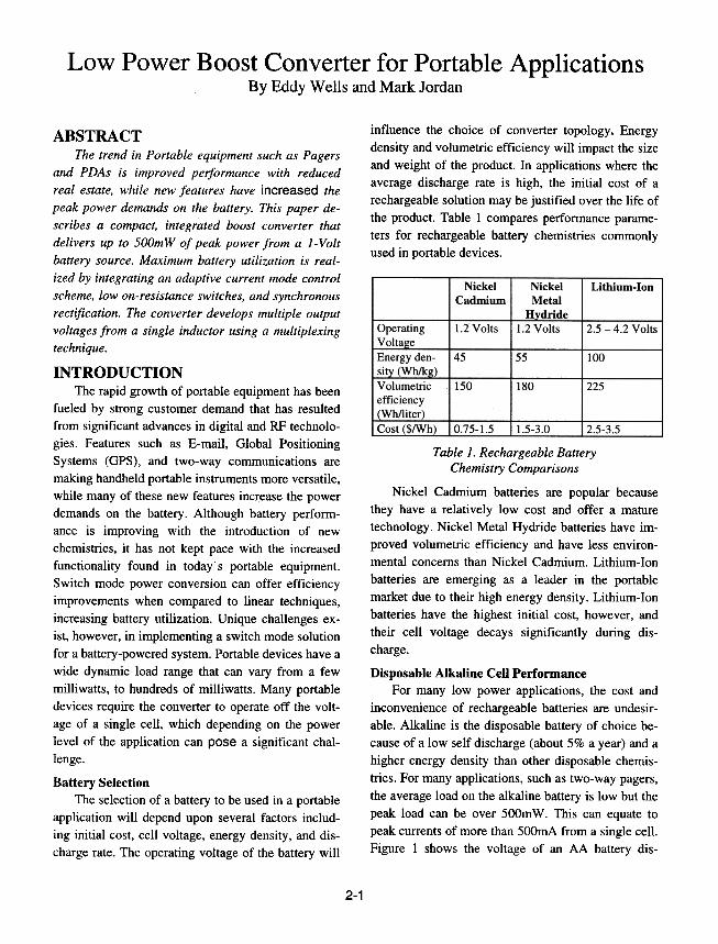
Low Power Boost Converter for Portable Applications ByEddy Wells and Mark Jordan influence the choice of converter topology. Energy density and volumetric efficiency will impact the size and weight of the product. In applications where the average discharge rate is high, the initial cost of a rechargeable solution may be justified over the life of the product. Table 1 compares performance parame- ters for rechargeable battery chemistries commonly used in portable devices. Nickel Cadmium Lithium-Ion 1.2 Volts Nickel Metal Hydride 1.2 Volts 12.5-4.2Volts Operating Volta!!e Energy den- sit (Wh/k ) Volumetric efficiency -(~~ 45 55 100 150 180 1225 I Cost ($/Wh) 10.75-1.5 I 1.5-3.0 -~ Table 1. Rechargeable Battery Chemistry Comparisons Nickel Cadmium batteries are popular because they have a relatively low cost and offer a mature technology. Nickel Metal Hydride batteries have im- proved volumetric efficiency and have less environ- mental concerns than Nickel Cadmium. Lithium-Ion batteries are emerging as a leader in the portable market due to their high energy density. Lithium-Ion batteries have the highest initial cost, however, and their cell voltage decays significantly during dis- charge. Disposable Alkaline Cell Performance For many low power applications, the cost and inconvenience of rechargeable batteries are undesir- able. Alkaline is the disposable battery of choice be- cause of a low self discharge (about 5% a year) and a higher energy density than other disposable chemis- tries. For many applications, such as two-way pagers, the average load on the alkaline battery is low but the peak load can be over 500m W .This can equate to peak currents of more than 500mA from a single cell. Figure 1 shows the voltage of an AA battery dis- ABSTRACT The trend in Portable equipment such as Pagers and PDAs is improved peiformance with reduced real estate, while new features have increased the peak power demands on the battery. This paper de- scribes a compact, integrated boost converter that delivers up to 500mW of peak power from a l-Volt battery source. Maximum battery utilization is real- ized by integrating an adaptive current mode control scheme, low on-resistance switches, and synchronous rectification. The converter develops multiple output voltages from a single inductor using a multiplexing technique. INTRODUCTION The rapid growth of portable equipment has been fueled by strong customer demand that has resulted from significant advances in digital and RF technolo- gies. Features such as E-mail, Global Positioning Systems (GPS), and two-way communications are making handheld portable instruments more versatile, while many of these new features increase the power demands on the battery .Although battery perforrn- ance is improving with the introduction of new chemistries, it has not kept pace with the increased functionality found in today's portable equipment. Switch mode power conversion can offer efficiency improvements when compared to linear techniques, increasing battery utilization. Unique challenges ex- ist, however, in implementing a switch mode solution for a battery-powered system. Portable devices have a wide dynamic load range that can vary from a few milliwatts, to hundreds of milliwatts. Many portable devices require the converter to operate off the volt- age of a single cell, which depending on the power level of the application can pose a significant chal- lenge. Battery Selection The selection of a battery to be used in a portable application will depend upon several factors includ- ing initial cost, cell voltage, energy density, and dis- charge rate. The operating voltage of the battery will 2-1
Transcript of Low Power Boost Converter for Portable Applications By ... · Low Power Boost Converter for...
Low Power Boost Converter for Portable ApplicationsBy Eddy Wells and Mark Jordan
influence the choice of converter topology. Energy
density and volumetric efficiency will impact the size
and weight of the product. In applications where the
average discharge rate is high, the initial cost of a
rechargeable solution may be justified over the life of
the product. Table 1 compares performance parame-
ters for rechargeable battery chemistries commonly
used in portable devices.
NickelCadmium
Lithium-Ion
1.2 Volts
Nickel
Metal
Hydride
1.2 Volts 12.5-4.2VoltsOperatingVolta!!e
Energy den-
sit (Wh/k )
Volumetric
efficiency
-(~~
45 55 100
150 180 1225
I Cost ($/Wh) 10.75-1.5 I 1.5-3.0 -~
Table 1. Rechargeable Battery
Chemistry Comparisons
Nickel Cadmium batteries are popular because
they have a relatively low cost and offer a mature
technology. Nickel Metal Hydride batteries have im-
proved volumetric efficiency and have less environ-
mental concerns than Nickel Cadmium. Lithium-Ion
batteries are emerging as a leader in the portable
market due to their high energy density. Lithium-Ion
batteries have the highest initial cost, however, and
their cell voltage decays significantly during dis-
charge.
Disposable Alkaline Cell PerformanceFor many low power applications, the cost and
inconvenience of rechargeable batteries are undesir-
able. Alkaline is the disposable battery of choice be-
cause of a low self discharge (about 5% a year) and a
higher energy density than other disposable chemis-
tries. For many applications, such as two-way pagers,
the average load on the alkaline battery is low but the
peak load can be over 500m W .This can equate to
peak currents of more than 500mA from a single cell.
Figure 1 shows the voltage of an AA battery dis-
ABSTRACT
The trend in Portable equipment such as Pagers
and PDAs is improved peiformance with reduced
real estate, while new features have increased the
peak power demands on the battery. This paper de-
scribes a compact, integrated boost converter that
delivers up to 500mW of peak power from a l-Volt
battery source. Maximum battery utilization is real-
ized by integrating an adaptive current mode control
scheme, low on-resistance switches, and synchronous
rectification. The converter develops multiple output
voltages from a single inductor using a multiplexing
technique.
INTRODUCTIONThe rapid growth of portable equipment has been
fueled by strong customer demand that has resulted
from significant advances in digital and RF technolo-
gies. Features such as E-mail, Global Positioning
Systems (GPS), and two-way communications are
making handheld portable instruments more versatile,
while many of these new features increase the power
demands on the battery .Although battery perforrn-
ance is improving with the introduction of new
chemistries, it has not kept pace with the increased
functionality found in today's portable equipment.
Switch mode power conversion can offer efficiency
improvements when compared to linear techniques,
increasing battery utilization. Unique challenges ex-
ist, however, in implementing a switch mode solution
for a battery-powered system. Portable devices have a
wide dynamic load range that can vary from a few
milliwatts, to hundreds of milliwatts. Many portable
devices require the converter to operate off the volt-
age of a single cell, which depending on the power
level of the application can pose a significant chal-
lenge.
Battery SelectionThe selection of a battery to be used in a portable
application will depend upon several factors includ-
ing initial cost, cell voltage, energy density, and dis-
charge rate. The operating voltage of the battery will
2-1
charged at 500mA. Open circuit voltage was meas-
ured by removing the load for 10 seconds each min-
ute.
Discontinuous Mode EfficiencyAn analysis of the converter losses can provide
insight into detennining a control scheme that will
operate efficiently. Figure 2 shows a low voltage
synchronous boost converter along with the equiva-
lent circuit elements that are major contributors to
power loss. Switch capacitance has been reflected to
the gate for simplicity.
Figure 2. Synchronous Boost Converterand Equivalent Circuit Elements
In order to support a wide dynamic load range
with a reasonably small value of inductance, the
boost converter needs to operate in discontinuous
conduction mode at medium and light loads. Figure 3
shows inductor current in discontinuous conduction
mode.
Figure 1. AA Alkaline Battery Voltageat a SOOmA Discharge Rate
Battery Equivalent Series Resistance (ESR) is
shown in Figure 1 to have a large influence on the
actual voltage measured at the terminals. A battery
with 1.1 volts at no load, for example, will drop to
0.9 volts with a SOOmA load. The power conversion
circuitry will need to handle the low voltage droop
during these peak power durations. This can often be
the limiting factor in the ability to deliver sufficient
output power to the application.
ACHIEVING HIGH EFFICIENCY
OVER A WIDE DYNAMIC RANGE
Regardless of the battery chemistry selected, the
converter efficiency will influence the run time of the
device. Portable equipment may require lOO's of
milliamps when the device is fully functioning. In
standby mode, where the device spends a majority of
time, the equipment may require less than lmA. The
amount of time the device spends in various modes is
heavily dependent upon the user. Because it is diffi-
cult to predict how the device will be used, it is im-
portant that the converter operates efficiently over a
wide dynamic load range.
Figure 3. Discontinuous Mode Inductor Current
Discontinuous mode efficiency can be calculated
from the input and loss energy for a single conversion
cycle. Based of Figures 2 and 3, Table 2 gives ap-
proximate energy values and the resulting overall
efficiency.
2-2
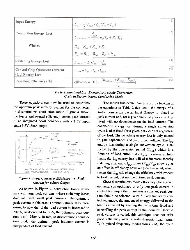
Table 2. Input and Lost Energy for a single Conversion
Cycle in Discontinuous Conduction Mode
These equations can now be used to detennine The reason this occurs can be seen by looking at
the optimum peak inductor current for the converter the equations in Table 2 that detail the energy of a
in discontinuous conduction mode. Figure 4 shows single conversion cycle. Input Energy is related to
the losses and overall efficiency versus peak current peak current and, for a given value of peak current, is
of an integrated boost converter with a 1.5V input fixed with no dependence on the load current. The
and a 3.3V, 5mA output. conduction energy lost during a single conversion
cycle is also fixed for a given peak current regardless
of the load. The switching energy lost is only related
to gate capacitance and gate drive voltage. The IDD
energy lost during a single conversion cycle is af-
fected by the conversion period (T I ) which is acyc e
function of load current. As T I increases at li g ht
cyc e
loads, the IDD energy lost will also increase, thereby
reducing efficiency. IDD losses (ErnJEIN) show up as
an offset in efficiency however (see Figure 4), which
means that IDD will change the efficiency with respect
to load current, but not the optimal peak current.
Since discontinuous mode efficiency (for a given
converter) is optimized at only one peak current, a
control technique that maintains a constant peak cur-
rent should be selected. With a fixed frequency con-
trol technique, the amount of energy delivered to the
load is adjusted by keeping the cycle time fixed and
controlling the peak current in the inductor. Because
peak current is varied, this technique does not offer
good efficiency over a wide dynamic load range.
With pulsed frequency modulation (PFM) the cycle
Figure 4. Boost Converter Efficiency -vs- PeakCurrentfor a SmA Output
As shown in Figure 4, conduction losses domi-
nate with large peak currents, where switching losses
dominate with small peak currents. The optimum
peak current in this case is around 250mA. It is inter-
esting to note that if the load current is increased to
20mA, or decreased to 1 mA, the optimum peak cur-
rent is still 250mA. In fact, in discontinuous conduc-
tion mode, the optimum peak inductor current is
independent of load current.
2-3
a given switch geometry and silicon process. By gen-
erating an 8V supply (V GD) for the gate drive, rather
than using the main output voltage (VOUT)' conduc-
tion losses are lowered by a factor of 2-3. Eight volts
achieves the best overall efficiency compromise be-
tween switching and conduction losses for the con-
verter. The 8V output can be used to support an
additional IOmA of load current for applications re-
quiring an auxiliary output. By lowering conduction
losses, the converter can deliver more current to the
load at low battery voltages.
time, rather than the peak current, is adjusted to ac-
commodate load variations. This allows an optimal
peak current to be .chosen that will maximize effi-
ciency in discontinuous conduction mode.
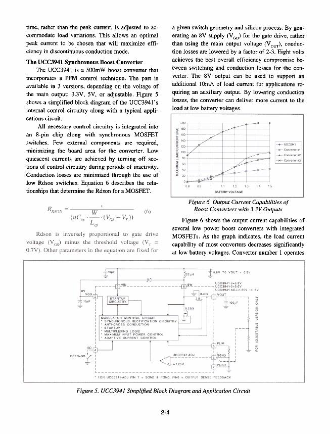
The UCC3941 Synchronous Boost Converter
The UCC3941 is a 500mW boost converter that
incorporates a PFM control technique. The part is
available in 3 versions, depending on the voltage of
the main output: 3.3V, 5V, or adjustable. Figure 5
shows a simplified block diagram of the UCC3941 's
internal control circuitry along with a typical appli-
cations circuit.
All necessary control circuitry is integrated into
an S-pin chip along with synchronous MOSFET
switches. Few external components are required,
minimizing the board area for the converter. Low
quiescent currents are achieved by turning off sec-
tions of control circuitry during periods of inactivity.
Conduction losses are minimized through the use of
low Rdson switches. Equation 6 describes the rela-
tionships that determine the Rdson for a MOSFET .
Figure 6. Output Current Capabilities ofBoost Converters with 3.3V Outputs
Figure 6 shows the output current capabilities of
several low power boost converters with integrated
MOSFETs. As the graph indicates, the load current
capability of most converters decreases significantly
at low battery voltages. Converter number 1 operates
Figure 5. UCC3941 Simplified Block Diagram and Application Circuit
2-4
ous/discontinuous mode boundary has been
eliminated. A detailed description of how the con-
verter transitions between modes and controls the
current in the inductor is given in the section titled
"Multiplexed Waveforms".
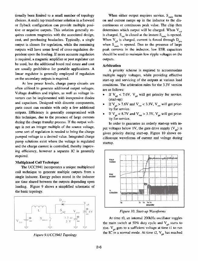
Efficiency CurvesContinuous conduction mode allows increased
output power, while discontinuous PFM mode deliv-
ers optimal efficiency at light loads. The modes of
operation are controlled with an internal state ma-
chine that adjusts charge times and current limits. By
providing efficient conversion over the usable battery
voltage in both modes, operation time is maximized.
Figure 8 shows UCC3941 efficiencies over a 200:1
load range.
in discontinuous conduction mode and has limited
current capabilities. Converters number 2 and 3 in-
crease their output current capabilities with continu-
ous mode operation, but their ability decreases at low
input voltages. The UCC3941 achieves improved
capability by combining low Rdson switches with
continuous mode operation.
Continuous Mode Operation
Discontinuous conduction mode results in a sim-
ple control scheme, however, the average load cur-
rent (reflected to the input) is limited to less than half
the peak current. If the peak inductor current is in-
creased, efficiency and the output voltage ripple will
suffer. In order to provide increased load current, the
UCC3941 is allowed to transition into continuous
conduction mode (see Figure 7). In order to keep the
control scheme simple, while providing the ability to
generate multiple outputs, a pseudo continuous con-duction mode is implemented.
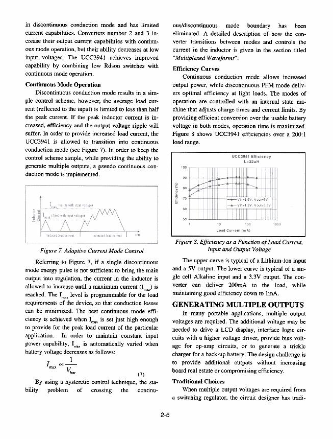
Figure 7. Adaptive Current Mode Control
Referring to Figure 7, if a single discontinuous
mode energy pulse is not sufficient to bring the main
output into regulation, the current in the inductor is
allowed to increase until a maximum current (Imax) is
reached. The Imax level is programmable for the load
requirements of the device, so that conduction losses
can be minimized. The best continuous mode effi-
ciency is achieved when lmax is set just high enough
to provide for the peak load current of the particular
application. In order to maintain constant input
power capability, lmax is automatically varied when
battery voltage decreases as follows:
1I- oc -max V;
bat (7)
By using a hysteretic control technique, the sta-
bility problem of crossing the continu-
Figure 8. Efficiency as a Function of Load Current,Input and Output Voltage
The upper curve is typical of a Lithium-Ion input
and a 5V output. The lower curve is typical of a sin-
gle cell Alkaline input and a 3.3V output. The con-
verter can deliver 200mA to the load, while
maintaining good efficiency down to lmA.
GENERATING MULTIPLE OUTPUTSIn many portable applications, multiple output
voltages are required. The additional voltage may be
needed to drive a LCD display, interface logic cir-
cuits with a higher voltage driver, provide bias volt-
age for op-amp circuits, or to generate a trickle
charger for a back-up battery. The design challenge is
to provide additional outputs without increasing
board real estate or compromising efficiency.
Traditional ChoicesWhen multiple output voltages are required from
a switching regulator, the circuit designer has tradi-
2-5
When either output requires service, S .turnsmaInon and current ramps up in the inductor to the dis-
continuous or continuous peak value. The chip then
determines which output will be charged. When Vout
is charged, S t is closed at the instant S is opened.ou maIn
When V d is charged, current is forced through D9 poswhen S is opened. Due to the presence of largemaInpeak currents in the inductor, low ESR capacitors
should be used to maintain low ripple voltages on the
outputs.
Arbitration
A priority scheme is required to accommodate
multiple supply voltages, while providing effective
start-up and servicing of the outputs at various load
conditions. The arbitration rules for the 3.3V version
are as follows:
.If V gd < 7 .6V , V gd will get priority for service.
(start-up).If V gd > 7.6V and Vout < 3.3V, Vout will get prior-
ity for service-
.If V gd < 8.7V and Vout > 3.3V, V gd will get prior-
ity for service.
In order to guarantee an orderly start-up with in-
put voltages below 1 V, the gate drive supply (V gd) is
given priority during start-up. Figure 10 shows os-
cilloscope waveforms of current and voltage during
startup.
VOUT
1V/DIV
tionally been limited to a small number of topology
choices. A multi tap transformer solution in a forward
or f!yback configuration can provide multiple posi'-
tive or negative outputs. This solution generally re-
quires custom magnetics with the associated design,
cost, and purchasing headaches. Typically, a single
output is chosen for regulation, while the remaining
outputs will have some level of cross-regulation de-
pendent upon the loading. If more accurate regulation
is required, a magnetic amplifier or post regulator can
be used, but the additional board real estate and cost
are usually prohibitive for portable applications. A
linear regulator is generally employed if regulation
on the secondary outputs is required.
At low power levels, charge pump circuits are
often utilized to generate additional output voltages.
Voltage doublers and triplers, as well as voltage in-
verters can be implemented with inexpensive diodes
and capacitors. Designed with discrete components,
parts count can escalate with only a few additional
outputs. Efficiency is generally compromised with
this technique, due to the presence of large currents
during the charge transfer process. If the output volt-
age is not an integer multiple of the source voltage,
some sort of regulation is needed to bring the charge
pumped voltage to a desired value. Integrated charge
pump solutions exist where the voltage is regulated
and the charge current is controlled, thereby improv-
ing efficiency, however a separate IC is generally
required.
Multiplexed Coil Technique
The UCC3941 incorporates a unique multiplexed
coil technique to generate multiple outputs from a
single inductor. Energy pulses stored in the inductor
are time shared between the outputs depending upon
loading. Figure 9 shows a simplified schematic of
the basic topology.
VGD
5V/OIV
ILOSA/DIV
T, T' T3T42msIDIV
Figure 10. Start-up Waveforms
At time to, an internal 200kHz oscillator toggles
the main switch at 50% duty cycle and V gd starts to
rise. V gd gets to a sufficient voltage at time tl to run
the IC in a normal mode. At time t2, V gd has reachedFigure 9.UCC3941 Topology
2-6

wavefonns of the converter servicing two outputs. At
time tl, Vout drops below its lower threshold, and the
inductor is charged for 12uSecNin. At time t2, the
inductor begins to discharge with a minimum off
time of 1.7uS. Under lightly loaded conditions the
amount of energy delivered in this single pulse would
satisfy the voltage control loop, and the converter
would not command any more energy pulses until the
output again drops below the lower voltage threshold.At time t3, the V gd supply has dropped below its
lower threshold, but Vout is still above its threshold
point. This results in an energy pulse to the gate drive
supply at t4. However, while the gate drive is being
serviced, Vout has dropped below its lower threshold,
so the state machine commands an energy pulse to
Vout as soon as the gate drive pulse is completed
(time t5).Time t6, represents a transition between light and
heavy loads. A single energy pulse is not sufficient to
force the output voltage above its upper threshold
before the minimum off time has expired, and a sec-
ond charge cycle is commanded. Since the inductor
does not reach zero current in this case, the peak cur-
rent is greater than O.5A at the end of the next charge
on time. The result is a ratcheting of inductor current
until either the output voltage is satisfied, or the con-
its lower threshold of 7.6V and the arbitration allows
VOUT to get started. VOUT has reached 3.3V at time t3,
and V gd is allowed to charge to 8. 7V .At time t4, both
outputs are in regulation and the converter operates
normally, servicing the outputs as the load demands.
Multiplexed Waveforms
The UCC3941 converter develops a hysteretic
control technique by monitoring the output voltages
with comparators. If an output falls below its voltage
threshold, the converter will deliver a single or multi-
ple energy pulses to the output until the output comes
into regulation. The inductor charge time is con-
trolled by: Ton=12uSecNin. In discontinuous con-
duction mode, this results in a constant peak current,
regardless of the input voltage. For a 22uH inductor,
the resulting peak current is approximately SOOmA.
The on time control is maintained, unless the inductor
current reaches the I limit. The inductor dischargemax
time is fixed at Toff=I.7uSec, unless the output rises
above its voltage threshold. The short off time allows
the inductor current to transition to the lmax limit if a
single pulse is not adequate. If the output voltage is
satisfied after the 1.7uS off time, the charge switch
will not be activated, and the inductor current will
decay to zero.
Figure II depicts typical voltage and current
:Vgd ' : : 50mV
Voltage ; --L.J'.:P , Ri
pple: typical:
!2 13
ti
Vout
VoltageRipple
Imax
u
InductorCurrent
Figure 11. Multiplexed 1nductor Servicing Two Outputs
2-7

D
Figure 12. Single 1nductor Servicing 4 Outputs
The UCC394I addresses these issues by incorpo-
rating an adaptive control scheme that extends the
battery's usable voltage range. High efficiency over a
wide dynamic load range is achieved with a constant
power continuous current mode and a fixed peak cur-
rent discontinuous mode. A unique power conversion
topology is used, where multiple outputs are gener-
ated from a single inductor, resulting in efficient use
of board space.
REFERENCES[I] "Make the Right Battery Choice for Port-
abIes" Dan Pnina, Tadiran Electronic Industries.
[2] "UCC394l 1 Volt Synchronous Boost con-verter" Data Sheet, Unitrode Integrated Circuit
Corporation.
verter reaches its programmed current limit. At time
t7, the gate drive voltage has dropped below its
threshold but the converter continues to service Vout
because it has highest priority, unless Vgd drops be-
low 7 .6V .
Between t7 and t8, the converter reaches its
maximum current limit that is determined by the pro-
grammed power limit and VIN. Once the limit is
reached, the converter operates in continuous mode
with approximately 200mA of ripple current. A time
t8, the output voltage is satisfied, and the converter
can service V gd, which occurs at t9.
Topology ExtensionsThe multiplexed coil topology can be extended to
produce additional outputs. Figure 12 shows a single
inductor providing energy to 3 positive outputs and a
negative output. The generation of the main output
(Vou,) and gate drive output (V gd) has been explained.
The V nicd output is a trickle charger for a Nickel
Cadmium battery back-up. In order to produce a
fixed, low current, trickle charge the converter deliv-
ers low peak current pulses to the V nicd output at fixed
intervals of time.A negative voltage (V neg) is produced by using a
fly-back technique with Vout and V bat. Negative cur-
rent is generated by back-charging the inductor
through the Sou, switch. When the inductor current
reaches some negative peak, Soot is open. Current is
then pulled through D , charging the V output. Inneg negorder for the flyback technique to operate correctly,
the charge stored in the Vout capacitor should be sev-
eral times larger than the charge stored in the V neg
capacitor.
CONCLUSIONWhen selecting a power management solution for
a portable application, it is important that the con-
verter operates efficiently over a wide dynamic
range. In order to get the most energy from a low
voltage power source, the converter should be able to
start up and operate below IV during peak load de-
mands. When additional outputs are required, issues
relating to converter efficiency and board real estate
can often be critical.
2-8

IMPORTANT NOTICE
Texas Instruments and its subsidiaries (TI) reserve the right to make changes to their products or to discontinueany product or service without notice, and advise customers to obtain the latest version of relevant informationto verify, before placing orders, that information being relied on is current and complete. All products are soldsubject to the terms and conditions of sale supplied at the time of order acknowledgment, including thosepertaining to warranty, patent infringement, and limitation of liability.
TI warrants performance of its products to the specifications applicable at the time of sale in accordance withTI’s standard warranty. Testing and other quality control techniques are utilized to the extent TI deems necessaryto support this warranty. Specific testing of all parameters of each device is not necessarily performed, exceptthose mandated by government requirements.
Customers are responsible for their applications using TI components.
In order to minimize risks associated with the customer’s applications, adequate design and operatingsafeguards must be provided by the customer to minimize inherent or procedural hazards.
TI assumes no liability for applications assistance or customer product design. TI does not warrant or representthat any license, either express or implied, is granted under any patent right, copyright, mask work right, or otherintellectual property right of TI covering or relating to any combination, machine, or process in which suchproducts or services might be or are used. TI’s publication of information regarding any third party’s productsor services does not constitute TI’s approval, license, warranty or endorsement thereof.
Reproduction of information in TI data books or data sheets is permissible only if reproduction is withoutalteration and is accompanied by all associated warranties, conditions, limitations and notices. Representationor reproduction of this information with alteration voids all warranties provided for an associated TI product orservice, is an unfair and deceptive business practice, and TI is not responsible nor liable for any such use.
Resale of TI’s products or services with statements different from or beyond the parameters stated by TI forthat product or service voids all express and any implied warranties for the associated TI product or service,is an unfair and deceptive business practice, and TI is not responsible nor liable for any such use.
Also see: Standard Terms and Conditions of Sale for Semiconductor Products. www.ti.com/sc/docs/stdterms.htm
Mailing Address:
Texas InstrumentsPost Office Box 655303Dallas, Texas 75265
Copyright 2001, Texas Instruments Incorporated