
Loosely Coupled Transformer and Tuning Network Design … · 4.2 INDUCTIVE EV BATTERY CHARGER...
211
Loosely Coupled Transformer and Tuning Network Design for High-Efficiency Inductive Power Transfer Systems Cong Zheng Dissertation submitted to the Faculty of the Virginia Polytechnic Institute and State University in partial fulfillment of the requirements for the degree of Doctor of Philosophy In Electrical Engineering Jih-Sheng Lai, Chair Louis J. Guido Kwang-Jin Koh William T. Baumann Douglas J. Nelson May 8, 2015 Blacksburg, Virginia Keywords: Inductive power transfer, loosely coupled transformer, compensation network, high efficiency, gap variation, misalignment Copyright 2015, Cong Zheng
Transcript of Loosely Coupled Transformer and Tuning Network Design … · 4.2 INDUCTIVE EV BATTERY CHARGER...

Loosely Coupled Transformer and Tuning
Network Design for High-Efficiency Inductive
Power Transfer Systems
Cong Zheng
Dissertation submitted to the Faculty of the
Virginia Polytechnic Institute and State University
in partial fulfillment of the requirements for the degree of
Doctor of Philosophy
In
Electrical Engineering
Jih-Sheng Lai, Chair
Louis J. Guido
Kwang-Jin Koh
William T. Baumann
Douglas J. Nelson
May 8, 2015
Blacksburg, Virginia
Keywords: Inductive power transfer, loosely coupled transformer,
compensation network, high efficiency, gap variation, misalignment
Copyright 2015, Cong Zheng

Loosely Coupled Transformer and Tuning Network
Design for High-Efficiency Inductive Power Transfer
Systems
Cong Zheng
ABSTRACT
Transfer signal without wire has been widely accepted after the
introduction of cellular technology and WiFi technology, hence the power cable
is the last wire that has yet to be eliminated. Inductive power transfer (IPT)
has drawn substantial interest in both academia and industry due to its
advantages including convenience, nonexistence of cable and connector, no
electric shock issue, ability to work under some extreme environment, and so
on. After performing thorough literature review of IPT systems, two major
drawbacks including low power efficiency and coil displacement sensitivity are
identified as the main obstacles that have to be solved in order for these
systems to reach full functionality and compete with existing wired solutions.
To address the limitations and design challenges in the IPT systems, a
detailed electric circuit modeling of individual part of the IPT DC-DC stage is
performed. Several resonant DC-AC inverters and output AC-DC rectifiers are
compared based on their performance and feasibility in inductive charging
applications. Different equivalent circuit models for the loosely coupled
iii
transformer (LCT) are derived which allows for better understanding on how
power is distributed among the circuit components. Five compensation
networks to improve the power transfer efficiency are evaluated and their
suitable application occasions are identified.
With comprehensive circuit model analysis, the influence of the resonant
compensation tank parameters has been investigated carefully for efficient
power transfer. A novel tuning network parameters design methodology is
proposed based on multiple given requirement such as battery charging profile,
geometry constraints and operating frequency range, with the aim of avoiding
bifurcation phenomenon during the whole charging process and achieving
decent efficiency. A 4-kW hardware prototype based on the proposed design
approach is built and tested under different gap and load conditions. Peak IPT
system DC-DC efficiencies of 98% and 96.6% are achieved with 4-cm and 8-cm
air gap conditions, which is comparable to the conventional plug-in type or
wired charging systems for EVs. A long-hour test with real EV batteries is
conducted to verify the wireless signal transmission and CC/CV mode seamless
transition during the whole charging profile without bifurcation.
To reduce the IPT system sensitivity to the gap variation or misalignment,
a novel LCT design approach without additional complexity for the system is
proposed. With the aid of FEA simulation software, the influence of coil relative
position and geometry parameters on the flux distribution and coupling
coefficient of the transmitter and receiver is studied from an electromagnetic

iv
perspective. An asymmetrical LCT based on the proposed design method is
built to compare with a traditional symmetrical LCT. With fixed 10-mm gap
and 0 to 40-mm misalignment variation, the coupling coefficient for the
symmetrical LCT drops from 0.354 to 0.107, and the corresponding efficiency
decrease is 16.6%. The operating frequency variation is nearly 100 kHz to
maintain same input/output condition. When employing the proposed
asymmetrical LCT, the coupling coefficient changes between 0.312 and 0.273,
and the maximum efficiency deviation is kept within 0.67% over the entire 40-
mm misalignment range. Moreover, the required frequency range to achieve
same operation condition is less than 10 kHz.
Lastly, some design considerations to further improve the IPT system
efficiency are proposed on the basis of the designed asymmetrical LCT
geometry. For given circuit specifications and LCT coupling conditions,
determination of the optimal primary winding turns number could help
achieve minimal winding loss and core loss. For lower output power, the
optimal primary winding turns number tends to be larger compared to that for
higher output power IPT system. Two asymmetrical LCT with similar
dimension but different number of turns are built and tested with a 100-W
hardware prototype for laptop inductive charging. The proposed efficiency
improvement methodology is validated by the winding loss and core loss from
experimental results.

v
To my wife Liu Yang
To my parents Wei Zheng
Huiling Liu

vi
ACKNOWLEDGEMENTS
First, I would like to express my sincere gratitude and respect to my
esteemed advisor, Dr. Jih-Sheng Lai, for his supervision and experienced
guidance. His continuous support and constant encouragement brought me
more confidence in my research work and led me to complete my projects
successfully. Without him, I could not have gone so far and finished this Ph.D.
program.
I would also like to thank my advisory committee members: Dr. Louis J.
Guido, Dr. Kwang-Jin Koh, Dr. William T. Baumann and Dr. Douglas J.
Nelson for their insightful suggestions and comments throughout my pursuit
of the Ph.D. degree.
It has been a great pleasure for me to work with the talented colleagues in
the Future Energy Electronics Center (FEEC). I would like to thank Mr. Gary
Kerr, Dr. Wensong Yu, Dr. Chien-Liang Chen, Dr. Hao Qian, Dr. Pengwei Sun,
Dr. Ahmed Koran, Dr. Ben York, Dr. Younghoon Cho, Dr. Zheng Zhao, Dr.
Ethan Swint, Dr. Zakariya Dalala, Dr. Bin Gu, Dr. Thomas LaBella, Dr.
Jungmuk Choe, Dr. Qingqing Ma, Mr. Rui Chen, Mr. Eric Faraci, Mr. Lanhua
Zhang, Mr. Baifeng Chen, Mr. Zaka Ullah Zahid, Mr. Jason Dominic, Ms.
Hyun-Soo Koh, Mr. Zidong Liu, Mr. Yaxiao Qin, Ms. Xiaonan Zhao, Mr. Seung-
Ryul Moon, Mr. Andrew Amrhein, Ms. Rachael Born, Mr. Bo Zhou, Ms.
Hongmei Wan, Mr. Wei-Han Lai, Mr. Hidekazu Miwa, Mr. Hsin Wang, Ms. Le
Du, Mr. Alex Kim, Mr. Nathan Kees, Mr. Chris Hutchens, Mr. Brett Whitaker,

vii
and Mr. Daniel Martin. My studies and research were enjoyable with their
helpful discussions, great support and precious friendship. My gratitude also
goes out to the visiting scholars and professors, Dr. Hongbo Ma, Dr. Huang-
Jen Chiu, Dr. Yen-Shin Lai, Dr. Chien-Yu Lin, Dr. Chung-Yi Lin, Mr. Yuchen
Liu, Dr. Chuang Liu, Dr. Ruixiang Hao, Dr. Zhiling Liao, Dr. Deshang Sha, Dr.
Xueshen Cui, Dr. Yan Li, Dr. Chia-His Chang, Dr. Bo-Yuan Chen, and Dr.
Kuan-Hong Wu, for their tremendous help with my research as well as my
daily life.
Furthermore, I would also like to thank Dr. Gianpaolo Lisi and Mr. Dave
Anderson of Texas Instruments for providing support, guidance, and funding
for the work in this dissertation.
I would like to offer my deepest gratitude to my parents, Wei Zheng and
Huiling Liu and my parents in law, Chen Yang and Huiqin Zuo, for their
continuous love, support, and encouragement with every venture that I
undertake during my life. Finally and most importantly, I would like to give a
very special thanks to my wife, Liu Yang, for her extraordinarily patience and
unconditional support throughout this long journey. She is the eternal source
of inspiration in all aspect of my life.
Cong Zheng
05/08/2015 in Blacksburg

viii
CONTENTS
CHAPTER 1 INTRODUCTION ...................................................................... 1
1.1 OVERVIEW ................................................................................................... 1
1.2 RESEARCH MOTIVATION ............................................................................... 4
1.3 OBJECTIVES OF THE RESEARCH PROJECT ..................................................... 5
1.4 METHODOLOGY ............................................................................................ 7
1.5 MAJOR CONTRIBUTIONS ............................................................................... 9
1.6 OUTLINE OF THE DISSERTATION ................................................................. 10
1.7 LIST OF PUBLICATIONS ............................................................................... 12
CHAPTER 2 CONTACTLESS POWER TRANSFER TECHNOLOGY ......... 15
2.1 INTRODUCTION .......................................................................................... 15
2.2 BRIEF HISTORICAL ACHIEVEMENTS REVIEW ............................................... 17
2.3 CLASSIFICATION OF CONTACTLESS POWER TRANSMISSION SYSTEMS ........... 23
2.3.1 Capacitive coupling ........................................................................... 24
2.3.2 Microwave coupling ........................................................................... 26
2.3.3 Laser coupling ................................................................................... 28
2.4 STATE-OF-THE-ART IPT SYSTEMS ............................................................... 30
2.4.1 Inductive charging ............................................................................ 30
2.4.2 Induction heating .............................................................................. 44
2.4.3 Biomedical implants .......................................................................... 48
2.4.4 Radio-frequency identification .......................................................... 50
2.5 SUMMARY .................................................................................................. 51
CHAPTER 3 ANALYTICAL MODEL OF INDUCTIVE POWER TRANSFER
SYSTEMS .................................................................................................. 54
3.1 INTRODUCTION .......................................................................................... 54
3.2 HIGH FREQUENCY RESONANT INVERTER .................................................... 55
3.2.1 Full bridge inverter ........................................................................... 56
3.2.2 Half bridge inverter ........................................................................... 58
3.2.3 Class-E inverter ................................................................................. 60
3.2.4 Resonant inverter comparison .......................................................... 63
3.3 OUTPUT RECTIFIER .................................................................................... 65
3.3.1 Full bridge rectifier ........................................................................... 66
3.3.2 Half bridge rectifier ........................................................................... 68
3.3.3 Center-tapped full-wave rectifier ..................................................... 70
3.3.4 Output rectifier comparison .............................................................. 73
3.4 LOOSELY COUPLED TRANSFORMER MODEL ................................................. 75
3.5 COMPENSATION NETWORK ......................................................................... 83
3.6 SUMMARY .................................................................................................. 91

ix
CHAPTER 4 HIGH EFFICIENCY INDUCTIVE POWER TRANSFER
SYSTEM FOR ELECTRIC VEHICLE BATTERY CHARGING
APPLICATION ............................................................................................... 95
4.1 INTRODUCTION .......................................................................................... 95
4.2 INDUCTIVE EV BATTERY CHARGER CIRCUIT CONFIGURATION ..................... 98
4.2.1 Soft-switching features ..................................................................... 98
4.2.2 Key waveforms of the inductive EV charging circuit .................... 101
4.3 DESIGN OF THE COMPENSATION NETWORK PARAMETERS ......................... 102
4.3.1 Effect of parameters on compensation network efficiency ............ 102
4.3.2 Design methodology for SS Tuning Network Parameters ............. 106
4.3.3 Design example ............................................................................... 109
4.4 CONTROL OF THE INDUCTIVE CHARGING SYSTEM ..................................... 112
4.5 EXPERIMENTAL VERIFICATION ................................................................. 114
4.6 SUMMARY ................................................................................................ 125
CHAPTER 5 HIGH MISALIGNMENT TOLERANCE HIGH EFFICIENCY
INDUCTIVE LAPTOP CHARGER .............................................................. 127
5.1 INTRODUCTION ........................................................................................ 127
5.2 DESIGN CONSIDERATIONS FOR GAP VARIATION AND MISALIGNMENT
TOLERANCE .................................................................................................... 129
5.2.1 Primary coil inner diameter smaller than secondary coil outer diameter .................................................................................................... 131
5.2.2 Vary inner diameter of primary coil ............................................... 132
5.2.3 Vary inner diameter of primary coil ............................................... 135
5.3 INDUCTIVE LAPTOP CHARGER ................................................................... 138
5.3.1 Circuit diagram and operating waveforms .................................... 138
5.3.2 Effect of transformer turns on the winding loss ............................ 141
5.3.3 Effect of transformer turns on the core loss ................................... 145
5.4 EXPERIMENTAL VERIFICATION ................................................................. 148
5.4.1 Performance comparison between symmetrical and asymmetrical LCT ........................................................................................................... 148
5.4.2 Performance evaluation between 6 : 2 and 10 : 4 LCT .................. 154
5.5 SUMMARY ................................................................................................ 160
CHAPTER 6 CONCLUSIONS AND FUTURE WORK ............................... 163
6.1 CONCLUSIONS .......................................................................................... 163
6.2 FUTURE WORK ......................................................................................... 166
REFERENCE ............................................................................................... 169

x
LIST OF FIGURES
Figure 1.1 Principle operation of an IPT system. .............................................. 2
Figure 1.2 Typical block diagram of an IPT system. ......................................... 3
Figure 1.3 Loosely coupled transformer. ............................................................ 4
Figure 1.4 Methodology overview. ...................................................................... 8
Figure 2.1 1887 experimental setup of Hertz’s apparatus [26]. ...................... 18
Figure 2.2 Tesla’s work in CPT: (a) Tesla coils, (b) Wardenclyffe Tower [29].19
Figure 2.3 Schematic of power from space system [47]. .................................. 21
Figure 2.4 NASA’s laser powered aircraft [58]-[59]. ........................................ 22
Figure 2.5 Classification of contactless power transmission. .......................... 24
Figure 2.6 Typical diagram of a capacitive coupling CPT system................... 25
Figure 2.7 An illustration of microwave power transfer. ................................ 26
Figure 2.8 Schematic of (a) an electric toothbrush [85] and (b) an electric
shaver [87]. ................................................................................................. 31
Figure 2.9 Prototype of a mobile phone battery charger [89]. ......................... 32
Figure 2.10 Inductive charging kit from Palm Inc.: (a) Touchstone charging
dock [104], (b) a teardown view of the charger [104], (c) the receiver
located in the back cover of Palm Pre smartphone [105]. ........................ 34
Figure 2.11 The Magne Charge system: (a) the charging stating, (b) the
primary charging paddle [116]. ................................................................. 37
Figure 2.12 The WiT-3300 deployment kit from WiTricity [133]. ................... 39
Figure 2.13 OLEV system from KAIST [133]. ................................................. 41
Figure 2.14 Low power wireless charging standards: (a) WPC [140], (b) PMA
[141], (c) A4WP [142].................................................................................. 43
Figure 2.15 Principle of induction cooking [150]. ............................................ 46
Figure 2.16 IPT based biomedical implants: (a) cochlear hearing implant
[163], (b) drug infusion pump [166], (c) nerve stimulation device [169]. . 49
Figure 3.1 DC-DC stage diagram of the IPT system. ...................................... 55
Figure 3.2 Full bridge inverter diagram. ......................................................... 57
Figure 3.3 Full bridge inverter waveforms: (a) Q1 and Q3 gate signals, (b) Q2
and Q4 gate signals, (c) inverter output voltage vp, (d) vds of Q1 and Q3. . 57
Figure 3.4 Half bridge inverter diagram. ......................................................... 59
Figure 3.5 Half bridge inverter waveforms: (a) Q1 gate signals, (b) Q2 gate
signals, (c) inverter output voltage vp, (d) vds of Q1. .................................. 59
Figure 3.6 Class-E inverter diagram. ............................................................... 60
Figure 3.7 Class-E inverter waveforms: (a) inverter input current, (b) Q gate
signals, (c) vds of Q. ..................................................................................... 60
Figure 3.8 Full bridge rectifier diagram. .......................................................... 66
Figure 3.9 Full bridge rectifier waveforms: (a) rectifier input voltage vs, (b)
rectifier input current is, (c) voltage of diodes D1 and D3, (d) current of
diodes D1 and D3. ........................................................................................ 67
Figure 3.10 Half bridge rectifier diagram. ....................................................... 69
xi
Figure 3.11 Half bridge rectifier waveforms: (a) rectifier input voltage vs, (b)
rectifier input current is, (c) voltage of D1, (d) current of D1. ................... 69
Figure 3.12 Center-tapped full-wave rectifier diagram. .................................. 71
Figure 3.13 Center-tapped full-wave rectifier waveforms: (a) rectifier input
voltage vs1 and vs2, (b) rectified current is, (c) voltage of D1, (d) current of
D1. ............................................................................................................... 72
Figure 3.14 Loosely coupled transformer (a) coupled inductor model and (b)
decoupled model. ........................................................................................ 76
Figure 3.15 Lumped leakage inductance model for LCT. ................................ 79
Figure 3.16 LCT without compensation in and IPT system. ........................... 81
Figure 3.17 Efficiency and phase of total impedance for IPT system without
compensation network. .............................................................................. 82
Figure 3.18 Two-coil inductive coupling compensation networks of the IPT
system: (a) SS, (b) SP, (c) PS, (d) PP, and (e) LLC. ................................... 85
Figure 3.19 Equivalent circuit with decoupled LCT model for (a) SS, (b) SP
and (c) LLC. ................................................................................................ 88
Figure 4.1 Structure of an inductive charging system for EV. ........................ 95
Figure 4.2 Inductive EV charger main circuit topology. .................................. 98
Figure 4.3 Switching diagrams of the resonant inverter: (a) Q1 and Q3 gate
signals, (b) Q2 and Q4 gate signals, (c) inverter output voltage vp, (d)
inverter output current ip........................................................................... 99
Figure 4.4 Key waveforms of the inductive EV charging circuit: (a) gate
signals, (b) primary voltage vp and current ip, (c) secondary voltage vs and
current is, (d) primary capacitor voltage VCp and input DC voltage Vdc, (e)
secondary capacitor voltage VCs and output DC voltage Vo.................... 101
Figure 4.5 Compensation network efficiency, phase of total impedance,
output voltage and output power as function of operating frequency for
different load resistances. ........................................................................ 103
Figure 4.6 Efficiency, phase of total impedance and output power as function
of operating frequency for different compensation capacitances. .......... 104
Figure 4.7 Efficiency, phase of total impedance and output power as function
of operating frequency for different coupling coefficient. ....................... 105
Figure 4.8 Tuning network parameters design methodology flow chart. ..... 107
Figure 4.9 Transformer prototype dimensions and its FEA model. .............. 110
Figure 4.10 Transformer parameters and coupling coefficient versus different
gap distance and misalignment conditions. ............................................ 111
Figure 4.11 Transformer prototype dimensions and its FEA model. ............ 112
Figure 4.12 Assumed charging profile of EV battery packs. ......................... 112
Figure 4.13 Closed-loop control diagram. ....................................................... 113
Figure 4.14 DSP software structure. .............................................................. 114
Figure 4.15 Experimental setup on the bench. .............................................. 115
Figure 4.16 Main waveforms under full load condition with (a) 8-cm gap and
(b) 4-cm gap. ............................................................................................. 116
Figure 4.17 Capacitor voltage stress for 8-cm gap condition. ....................... 117

xii
Figure 4.18 System response when current reference: (a) step up; (b) step
down. ......................................................................................................... 118
Figure 4.19 System response when voltage reference: (a) step up; (b) step
down. ......................................................................................................... 118
Figure 4.20 A short charging cycle simulated with E-load. ........................... 119
Figure 4.21 System response when voltage reference: (a) step up; (b) step
down. ......................................................................................................... 121
Figure 4.22 Loss breakdown under different air gap conditions. .................. 122
Figure 4.23 Experimental setup with home-modified EV. ............................ 122
Figure 4.24 A long-hour charging cycle for the EV under test. ..................... 123
Figure 4.25 Closed-loop control with wireless signal communication. ......... 124
Figure 4.26 Long-hour charging profiles and efficiency measurement using a
home-modified EV. ................................................................................... 125
Figure 5.1 FEA simulation model. (a) 3-D view. (b) Top view without ferrite
cores. ......................................................................................................... 131
Figure 5.2 Coupling coefficient when primary coil inner diameter is smaller
than secondary coil outer diameter: (a) under gap variation but perfect
aligned condition, (b) under misaligned but fixed gap condition. .......... 132
Figure 5.3 Coupling coefficient for different primary coil inner diameter: (a)
under gap variation but perfect aligned condition, (b) under misaligned
but fixed gap condition. ............................................................................ 133
Figure 5.4 Magnetic Field Distribution when IDPri = 50 mm, IDSec = 50 mm.
................................................................................................................... 134
Figure 5.5 Coupling coefficient for different secondary coil inner diameter: (a)
under gap variation but perfect aligned condition, (b) under misaligned
but fixed gap condition. ............................................................................ 135
Figure 5.6 Magnetic Field Distribution when (a) IDPri = 100 mm, IDSec = 50
mm and (b) IDPri = 100 mm, IDSec = 75 mm. ........................................... 137
Figure 5.7 Proposed laptop charging architecture with IPT technology. ..... 138
Figure 5.8 Inductive laptop charger main circuit diagram. .......................... 139
Figure 5.9 Key waveforms of the LLC resonant converter: (a) gate signal of
Q1, (b) device voltage of Q1, (c) device current of Q1, (d) primary current ip
and magnetizing current im, (e) device voltage of D1, (f) device current of
D1. ............................................................................................................. 140
Figure 5.10 AC equivalent circuit of LLC resonant converter. ..................... 141
Figure 5.11 Total winding loss as a function of primary turns number and
operating frequency: (a) 3-D view and (b) 2-D view. ............................... 144
Figure 5.12 Ip and Im as functions of np. ......................................................... 146
Figure 5.13 Primary magnetic flux as a function of primary turns number
under: (a) 25-W output and (b) 100-W output. ........................................ 147
Figure 5.14 Experimental setup on the bench. .............................................. 148
Figure 5.15 Coupling coefficient for the symmetrical LCT. .......................... 150
Figure 5.16 Coupling coefficient for the asymmetrical LCT. ........................ 151
xiii
Figure 5.17 Main waveforms under full-load condition for the symmetrical
LCT with 10-mm gap and (a) 0-mm misalignment and (b) 40-mm
misalignment. ........................................................................................... 152
Figure 5.18 Coupling coefficient for the asymmetrical LCT. ........................ 153
Figure 5.19 Operating frequency under different load and misalignment
conditions. ................................................................................................. 154
Figure 5.20 Main waveforms under full load condition for: (a) 6 : 2 LCT and
(b) 10 : 4 LCT. ........................................................................................... 156
Figure 5.21 IPT system efficiency comparison with two LCTs under different
load conditions. ......................................................................................... 157
Figure 5.22 Loss breakdown of the IPT systems under: (a) 100 W; (b) 25 W.
................................................................................................................... 158
Figure 5.23 Calculated winding loss with different np under: (a) 100 W and
(b) 25 W ..................................................................................................... 159

xiv
LIST OF TABLES
Table 2-1 Comparison of low power wireless charging standards [144]-[145] 43
Table 3-1 Summary and comparison between the resonant inverters ........... 64
Table 3-2 Summary and comparison between the output rectifiers ............... 75
Table 3-3 Primary and secondary impedance .................................................. 86
Table 3-4 Total impedance of five circuit systems ........................................... 87
Table 4-1 Parameters value of compensation network .................................. 102
Table 5-1 FEA simulation parameters ........................................................... 131
Table 5-2 Parameters of two LCTs with different turns number ................. 155
1
Chapter 1 Introduction
1.1 Overview
An inductive power transfer (IPT) system, also called contactless power
transfer (CPT) system or wireless power transfer (WPT) system, is based on a
magnetically coupled transformer that transfers power from a transmitter coil
into a receiver coil with no physical contact. The two key principles behind the
operation of such an IPT system are Ampère’s circuital law and Faraday’s law
of induction [1]-[3]. Ampère’s circuital law, discovered by André-Marie Ampère
in 1826, relates that a magnetic field is generated around a closed loop
conductor carrying electric current with an intensity to the electric current
passing through the loop. On the other hand, Faraday’s law of induction
indicates that an alternating magnetic field will interact with a conductor to
produce an electromotive force (EMF) which is proportional to the magnetic
field’s strength and its rate of change.
Figure 1.1 explains how these two laws can be applied together to transfer
power inductively. An alternating current (AC) is flowing through a coil,
referred to as the transmitter or primary coil, generating an alternating
magnetic field. If another coil, referred to as the receiver or secondary coil, is
placed in close proximity with the transmitter, then the alternating magnetic
field will induce an EMF in the receiver coil and a current will flow when there
is a load connected to the coil. Therefore, power is being transferred inductively
from the primary coil to the secondary coil.

2
Figure 1.1 Principle operation of an IPT system.
The block diagram of a typical IPT system is illustrated in Figure 1.2. In
the power transmitter section, a frond-end AC-DC power factor correction
(PFC) stage converts the AC voltage provided by the electrical grid into a direct
current (DC) bus voltage. The high frequency DC-AC resonant inverter, also
referred to as the primary coil driver, supplied by the DC bus voltage,
generates a high frequency AC power output. The energy is then passed
through the loosely coupled transformer (LCT), from the transmitting coil to
the receiving coil and their respective tuning network circuits. The loosely
coupled primary and secondary coils pair is the major section of the IPT system
where Ampère’s and Faraday’s laws are applied. The inductively coupled coils
do not necessary have to be symmetrical, since they could have different
dimensions and shapes. The loosely coupled coils could be located at certain
range of distance and orientation with respect to each other. The high
frequency AC current flows in the transmitting coil of the LCT which converts
it into a high frequency alternating magnetic field. The alternating magnetic
field is picked up by the receiving coil of the LCT which then converts it into a
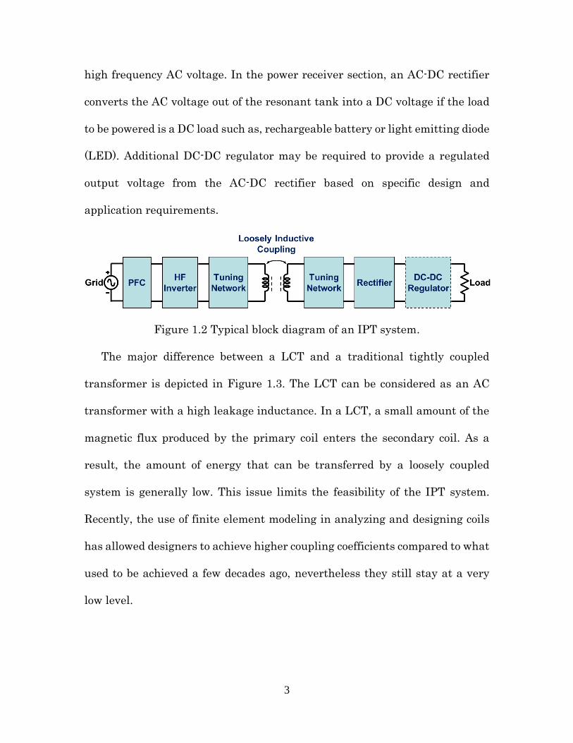
3
high frequency AC voltage. In the power receiver section, an AC-DC rectifier
converts the AC voltage out of the resonant tank into a DC voltage if the load
to be powered is a DC load such as, rechargeable battery or light emitting diode
(LED). Additional DC-DC regulator may be required to provide a regulated
output voltage from the AC-DC rectifier based on specific design and
application requirements.
Figure 1.2 Typical block diagram of an IPT system.
The major difference between a LCT and a traditional tightly coupled
transformer is depicted in Figure 1.3. The LCT can be considered as an AC
transformer with a high leakage inductance. In a LCT, a small amount of the
magnetic flux produced by the primary coil enters the secondary coil. As a
result, the amount of energy that can be transferred by a loosely coupled
system is generally low. This issue limits the feasibility of the IPT system.
Recently, the use of finite element modeling in analyzing and designing coils
has allowed designers to achieve higher coupling coefficients compared to what
used to be achieved a few decades ago, nevertheless they still stay at a very
low level.

4
Figure 1.3 Loosely coupled transformer.
IPT systems are more suitable for transmission of power over short
distances that are up to twice as large as the coils’ dimensions, since the
magnetic field’s strength produced by the primary coil becomes very weak at
further distances. According to the literatures in recent years, the efficiency of
an IPT system can reach up to 95% at short distances. However, it degrades
rapidly as the distance increases.
1.2 Research motivation
IPT technology has been matured to a level where applications and
products can now be developed and commercialized. In fact, it is one of the
fastest growing technologies that evolved from a concept, to prototype
demonstration, and finally to product development. The number publications
in IPT system are increasing exponentially, with a large number of
international conferences and exhibitions entirely dedicated for contactless
power transmission.
Despite its maturity, IPT system has not presented its full potential yet.
The applications and products that are being developed still do not
5
demonstrate what IPT technology can achieve. Even though the research and
development in IPT technology is at its peak since it was first conceptualized
in the 1990s, today’s application are only confined to stationary charging of
mobile devices and electric vehicles (EVs). It is about time to take IPT
technology into the next level by introducing applications and concepts that
can never be realized without it. Concepts such as dynamic vehicle charging,
in-flight charging for electric airborne vehicles and contactless power for
remote controlled planetary exploration robots are all examples of what IPT
technology can potentially achieve.
1.3 Objectives of the research project
Although the advantages of the IPT systems have been recognized, wide
adoption of the IPT systems still presents many challenges. The research work
in this project is to address these challenges that can lead to the next
generation of IPT technologies. The objectives of this research project can be
summarized as follows:
Improved feasibility
Nowadays, IPT systems are gaining considerable attention due to the
increasing dependence on various battery-powered applications, such as
wireless battery charging for (EVs) [4]-[11], portable electronic devices [12]-
[15], biomedical implants [16]-[23], and so on. Therefore, it is necessary to
undertake a critical review of the current state of IPT technology and identify
the areas and gaps for further research and investigation.
6
High system efficiency
Owing to the large leakage inductance existed in the LCT, circulating
energy is considerably large, hence resulting low system efficiency. This issue
is one of the major obstacles that hinder the IPT systems in practical
applications. Therefore, it is important to develop methods of maximizing the
power transfer efficiency across a LCT with its tuning network components. It
is the aim of this work to model the IPT system and to suggest a method to
optimize the compensation network parameters in order to improve the system
efficiency.
Large gap and misalignment variation tolerance
In practical applications using IPT systems, gap and horizontal
misalignments between transmitter and receiver would be a critical problem
because the power transfer efficiency greatly depends on the relative positions
of the primary and the secondary coils in the IPT system. In other words, the
power transfer efficiency is drastically reduced when a gap variation or
misalignment occurs between the inductive coils. Therefore, a novel design of
the LCT is required so as to counter the issue caused by gap and misalignment
variations.
Improved system control stability with wireless signal communication
Since one major advantage of the IPT system is there is no physical contact
between the transmitter and receiver, the use of wires to send the sensed
signals on the secondary side would defeat the purpose of IPT system.

7
Therefore, a wireless communication system should be adopted for signal
transmission. Moreover, accurate system modeling and stable controller
design is required due to different load conditions and gap/misalignment
variations.
1.4 Methodology
Many researches in IPT technology has been focusing on improving the
power transfer efficiency of the power electronics converters only. New circuit
topologies, semiconductor devices and design methods have been developed
that can certainly lead to better performance and higher power transfer
efficiency. However, with the rapid development of semiconductor devices in
recent years, the loss due to conduction and switching of these switches become
negligible compared to the loss induced by the LCT section in an IPT system.
Therefore the tuning network including the LCT and compensation capacitors
play a key role in determining its overall performance especially when
considering its ability to operate efficiently when load transient or
gap/misalignment variations occurs. Therefore, this dissertation focuses more
on the design of the resonant network sections of an IPT system other than the
power electronics converters.
Referring to the block diagram of an IPT system in Figure 1.2, each section
of the IPT system will be studied as an independent subsystem. High frequency
DC-AC resonant inverters that are commonly used as primary coil drivers will
be identified. Similarly, AC-DC rectifiers that are commonly used will be
8
summarized. Moreover, new design of the LCT and compensation network
parameters will be investigated.
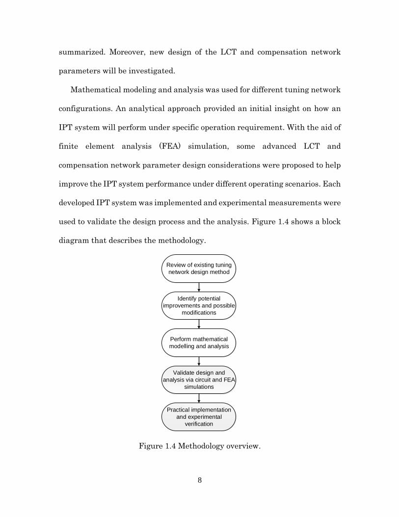
Mathematical modeling and analysis was used for different tuning network
configurations. An analytical approach provided an initial insight on how an
IPT system will perform under specific operation requirement. With the aid of
finite element analysis (FEA) simulation, some advanced LCT and
compensation network parameter design considerations were proposed to help
improve the IPT system performance under different operating scenarios. Each
developed IPT system was implemented and experimental measurements were
used to validate the design process and the analysis. Figure 1.4 shows a block
diagram that describes the methodology.
Review of existing tuning
network design method
Identify potential
improvements and possible
modifications
Perform mathematical
modelling and analysis
Validate design and
analysis via circuit and FEA
simulations
Practical implementation
and experimental
verification
Figure 1.4 Methodology overview.

9
1.5 Major contributions
The work in this research has resulted in the following contributions:
1. Different DC-AC inverter and AC-DC rectifier topologies for IPT system
are examined. Their performances and characteristics in certain
practical applications are analyzed.
2. A set of equivalent models of the inductively coupled link has been
introduced. The improved model can help determine how the efficiency
is affected by the tuning network parameters.
3. A detailed analysis of the criteria for bifurcation phenomenon to happen
in the IPT system and its affect to the system operation. Then the tuning
network parameter design method to avoid bifurcation phenomenon is
proposed.
4. Different coil geometry parameters are analyzed with the aid of FEA
simulation software. A novel LCT geometry is proposed in order to
reduce the gap variation and lateral misalignment effect during realistic
implementations.
5. A tuning network parameter design methodology is proposed to optimize
the IPT system efficiency based on given LCT dimension as well as load
and coupling variation specifications.
6. The IPT systems are modeled and closed-loop controllers are designed
incorporating wireless signal communication in order to achieve
adaptive control for different operation conditions.

10
1.6 Outline of the dissertation
The present chapter provides a general overview regarding the topic of IPT
and discusses the research motivation behind this work. The main objectives
and major contributions of this dissertation is given. A brief explanation of the
research problems discussed in each chapter is given as follows:
Chapter 2: Contactless Power Transfer Technology. This chapter begins
with a brief history of CPT technology which spans over a century is briefly
introduced. Methods of transferring power contactlessly other than
magnetic induction will be presented. Several commercial products and
applications that rely on magnetic induction are shown. A review of the
current state of IPT technology is given and several major standards are
discussed. Potential improvements and possible modifications for the IPT
technology are identified.
Chapter 3: Analytical Model of Inductive Power Transfer Systems. This
chapter analyzes the major part of an IPT system DC-DC stage
individually. The DC-AC resonant inverters and AC-DC output rectifiers
are compared based on their cost and performance to identify the feasible
application conditions. Different equivalent circuit models for the LCT are
investigated and their inherent equivalence is proved. The necessity of
capacitive compensation in an IPT system is demonstrated and five
possible tuning network configurations are evaluated in detail.

11
Chapter 4: High Efficiency Inductive Power Transfer System for Electric
Vehicle Battery Charging Application. This chapter proposes a SS
compensated inductive EV battery charging system utilizing frequency
modulated full bridge resonant inverter and full bridge rectifier. The
compensation network efficiency has been thoroughly analyzed and a
methodology to improve the efficiency is proposed. A 4-kW hardware
prototype has been built and tested under different gap and load conditions
and corresponding efficiencies are measured. A long-hour charging test
with real EV batteries is performed to verify the design validity of both
wireless power and signal transmissions.
Chapter 5: High Misalignment Tolerance High Efficiency Inductive Laptop
Charger. This chapter proposes a LLC resonant converter based inductive
laptop charging system. Firstly some design considerations for enhancing
the gap and misalignment tolerance are proposed. With the designed LCT
geometry, efficiency improvement methodology based on transformer
turns number is then presented. A 100-W hardware prototype for laptop
inductive charging is built. A symmetrical LCT and an asymmetrical LCT
are tested under different misalignment condition to validate the design
considerations. Two asymmetrical LCTs with the same dimension but
different number of turns are tested under different load condition to verify
the efficiency estimation methodology.

12
Chapter 6: Conclusions and Future Work. This chapter summarizes the
outcomes of the work presented in this research project and concludes the
thesis. Based on the experimental results, recommendations for future
work are also presented.
1.7 List of publications
Different parts of this work have already been published or are being
published in international journals or conference proceedings. These
publications are listed below.
Journal Papers
C. Zheng and J.-S. Lai, “Design Considerations to Reduce Gap Variation
and Misalignment Effects for the Inductive Power Transfer
System,” accepted for publication in IEEE Transactions on Power
Electronics.
C. Zheng, J.-S. Lai, R. Chen, W. E. Faraci, Z. U. Zahid, B. Gu, L. Zhang, G.
Lisi, and D. Anderson, “High-Efficiency Contactless Power Transfer
System for Electric Vehicle Battery Charging Application,” IEEE Journal
of Emerging and Selected Topics in Power Electronics, vol. 3, no. 1, pp. 65-
74, Mar. 2015.
Z. U. Zahid, Z. M. Dalala, C. Zheng, R. Chen, W. E. Faraci, J.-S. Lai, G.
Lisi, and D. Anderson, “Modeling and Control of Series–Series
Compensated Inductive Power Transfer System,” IEEE Journal

13
of Emerging and Selected Topics in Power Electronics, vol. 3, no. 1, pp.
111-123, Mar. 2015.
Conference Papers
C. Zheng and J.-S. Lai, “Asymmetrical Loosely Coupled Transformer for
Wireless Laptop Charger with Higher Misalignment Tolerance,” accepted
for publication in 2015 IEEE Energy Conversion Congress and Exposition,
2015.
C. Zheng, B. Chen, L. Zhang, Rui Chen, and J.-S. Lai, “Design
Considerations of LLC Resonant Converter for Contactless Laptop
Charger,” in 30th IEEE Applied Power Electronics Conference and
Exposition, 2015, pp. 3341-3347.
C. Zheng, R. Chen, and J.-S. Lai, “Design considerations to reduce gap
variation and misalignment effects for inductive power transfer
system,” in 40th Annual Conference of the IEEE Industrial Electronics
Society, 2014, pp. 1384-1390.
R. Chen, C. Zheng, Z. U. Zahid, E. Faraci, W. Yu, J.-S. Lai, M. Senesky, D.
Anderson, and G. Lisi, “Analysis and parameters optimization of a
contactless IPT system for EV charger,” in 29th IEEE Applied Power
Electronics Conference and Exposition, 2014, pp. 1654-1661.
C. Zheng, R. Chen, E. Faraci, Z. U. Zahid, M. Senesky, D. Anderson, J.-S.
Lai, W. Yu, and C.-Y. Lin, “High efficiency contactless power transfer

14
system for electric vehicle battery charging,” in 2013 IEEE Energy
Conversion Congress and Exposition, 2013, pp. 3243-3249.
Z. U. Zahid, C. Zheng, R. Chen, W. E. Faraci, J.-S. Lai, M. Senesky, and D.
Anderson, “Design and control of a single-stage large air-gapped
transformer isolated battery charger for wide-range output voltage for EV
applications,” in 2013 IEEE Energy Conversion Congress and Exposition,
2013, pp. 5481-5487.

15
Chapter 2 Contactless Power Transfer Technology
2.1 Introduction
Electrical energy has always been transferred by using the free electrons in
conductive materials. Electric current can flow in a conductor when an electric
potential difference is applied across the conductor, consequently electric
power can be transferred from a source such as a battery or a generator to a
load. For example, connecting a wire from the positive terminal of a battery to
the load and another from the load back to the negative terminal of the battery
will form a closed circuit. This will cause the free electrons in the wires and the
load to circulate due to the voltage potential of the battery. Since the battery
is forcing the flow of electrons through the load, energy is being transferred
from the battery and consumed by the load.
The use of cables and wires is the preferred method to connect a source to
a load. It is a simple and efficient method to transfer electrical energy and is
suitable for most of today’s applications since the loads, whether in industry or
in our homes, are stationary and motionless. However, as technology advances,
products are becoming smaller and portable. Relying on a cable connected to a
power outlet to obtain energy may not be a practical solution any more. New
applications are being introduced which are mobile and require a continuous
or semi-continuous power supply. Therefore, having a direct cable connection
may limit their freedom of movement and in some cases may not be a safe
option. For example, the research and development in EVs is on the rise due

16
to the increase of gas prices and to environmental concerns. These vehicles
have an on board battery that can provide power partially or entirely for the
total trip duration. Although a direct cable connection to a power outlet is
suitable to a certain degree to provide power and recharge the batteries, more
options will be available if that power was supplied contactlessly without
cables and wires. The vehicle, for example, could be charged dynamically while
it is moving. The risk of electric shock and sparks is highly reduced since no
physical contacts are used. Maintenance requirements are also reduced since
there is no wear and tear involved in the powering and charging process.
Primary side can be embedded underground so that it is weather proof and can
work under some extreme environments.
In contactless transfer of electrical energy, instead of using conductive
cables and wires, electrical energy from a power source is converted to another
form that can be propagated through a certain media without the need for
interconnecting wires. A simple example of delivering energy contactlessly is
the use of radio waves to transfer information such as sound, video and data.
A voltage signal representing the information to be transferred is generated in
a radio station. It is then converted into an electromagnetic energy signal and
emitted into the air, spreading in all directions. The electromagnetic energy
signal is picked up by an antenna at a reduced energy level and then converted
back into an electrical voltage signal and the information is extracted
afterwards.

17
Contactless transfer of energy or CPT may seem to be an alternative
method to power the electronic applications nowadays or in the future.
However, many design challenges and technological obstacles need to be
addressed and overcome. The following literature review targets to:
Present the different methods of contactless energy transmission.
Discuss current applications based on IPT.
Review the current research progress in IPT.
Identify the gaps and topics in IPT that require further investigation and
research.
2.2 Brief historical achievements review
The beginning of contactless power transmission can be dated back to 1868
when James Clerk Maxwell synthesized the Ampère’s circuital law and
Faraday's law of induction as well as other observations, experiments and
equations into a consistent theory, developed the classical electromagnetic
theory. Maxwell’s equations create the cornerstone for modern
electromagnetics, including the contactless transmission of electrical energy.
In 1884 John Henry Poynting derived equations for the flow of energy in an
electromagnetic field known as the Poynting’s theorem or the Poynting vector,
and they are utilized in the analysis of contactless energy transfer systems
[24]-[25]. Later in 1888, Heinrich Rudolf Hertz discovered radio waves, which
confirms the prediction of electromagnetic waves by Maxwell. Figure 2.1 shows
the experimental setup as Hertz made observations of the photoelectric effect

18
as well as the production and reception of electromagnetic waves. The receiver
consisted of a coil with a spark gap, where a spark would be seen when
electromagnetic waves is detected [26]-[28].
Figure 2.1 1887 experimental setup of Hertz’s apparatus [26].
The first significant breakthrough in contactless power transmission
technology was achieved by Nikola Tesla. During the period from 1891 to 1904
he experimented with transferring energy by inductive and capacitive coupling
employing spark-excited radio frequency resonant transformers, also referred
to as “Tesla coils” which generated high AC voltages as shown in Figure 2.2
(a). In demonstrations before the American Institute of Electrical
Engineers (now the IEEE) at the 1893 World’s Columbian Exposition in
Chicago, Tesla was able to demonstrate the illumination of phosphorescent
lamps without any electrical connections. At 1897 Tesla filed his first patents
based on the Wardenclyffe Tower as shown in Figure 2.2 (b), which is also
known as “Tesla Tower” in Colorado Springs. By using voltages of about 20
megavolts generated by a gigantic coil, he managed to light three incandescent

19
lamps at a distance of around one hundred feet. He concluded that electrical
energy could be transferred through the upper atmosphere and the Earth to
any point on the globe. His work also resulted in major contributions for long
distance radio telecommunication. Many researchers and inventors confirmed
his findings and discoveries later on [29]-[41].
Figure 2.2 Tesla’s work in CPT: (a) Tesla coils, (b) Wardenclyffe Tower [29].
The research continued in CPT especially for telecommunications during
the first few decades of the twentieth century. Radio stations and long distance
communications links were developed during World War I. The development
of microwave technology during World War II made radiative approaches
practical for the first time, and the first long distance contactless power
transmission was realized in the 1960s by William C. Brown [36]. Later in 1964
Brown invented the rectenna which could convert microwaves to DC power
efficiently. During the same year Brown demonstrated the first contactless-
powered unmanned helicopter using microwaves beamed from the ground as a
part of a joint project between the Department of Defense (DoD) and NASA.
An important motivation for microwave research in the 1970s and 1980s was

20
to obtain renewable solar energy. This concept proposed by the Department of
Energy (DoE) and NASA aimed to deploy giant space satellites to collect solar
energy and beam it to the earth using microwaves (Figure 2.3). Ground based
experiments conducted by NASA proved the possibility of such a system and
the ability to transfer high power levels over several kilometers. In landmark
1975 Brown demonstrated short range power transfer of 475 W using
microwaves at 54% DC to DC efficiency. He also demonstrated a huge power
CPT system at the Venus Site of JPL Goldstone Facility. 450 kW of power was
transferred across one mile using an antenna with 26-meter diameter. The 3.4-
meter by 7.2-meter receiving rectenna array achieved a rectified DC power of
30 kW at 82.5% efficiency. The system efficiency was only 6.67% efficiency
without taking the transmitter into consideration. However, due to the high
implementation and energy costs the concept of deploying these energy
collecting satellites was never realized [42]-[49]. The world’s first microwave
power transmission experiment in the ionosphere called the MINIX
(Microwave Ionosphere Nonlinear Interaction Experiment) rocket experiment
was demonstrated in 1983 at Japan [50]-[52]. Similarly, the world’s first fuel
free airplane powered by a 2.45-GHz microwave energy from ground was
reported in 1987 in Canada. This system which was referred to by the name
SHARP (Stationary High Altitude Relay Platform) was intended to be designed
as an airborne communications relay which would fly in circles of two
kilometers in diameter at an altitude of about 13 miles [53].
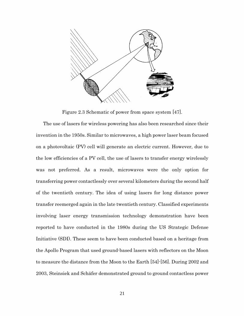
21
Figure 2.3 Schematic of power from space system [47].
The use of lasers for wireless powering has also been researched since their
invention in the 1950s. Similar to microwaves, a high power laser beam focused
on a photovoltaic (PV) cell will generate an electric current. However, due to
the low efficiencies of a PV cell, the use of lasers to transfer energy wirelessly
was not preferred. As a result, microwaves were the only option for
transferring power contactlessly over several kilometers during the second half
of the twentieth century. The idea of using lasers for long distance power
transfer reemerged again in the late twentieth century. Classified experiments
involving laser energy transmission technology demonstration have been
reported to have conducted in the 1980s during the US Strategic Defense
Initiative (SDI). These seem to have been conducted based on a heritage from
the Apollo Program that used ground-based lasers with reflectors on the Moon
to measure the distance from the Moon to the Earth [54]-[56]. During 2002 and
2003, Steinsiek and Schäfer demonstrated ground to ground contactless power

22
transmission via laser to a rover vehicle equipped with PV cells as a first step
towards the use of this technology for powering ground rovers for lunar and
planetary exploration missions in the future [57]. During the similar period,
Dryden Flight Research Center of NASA demonstrated a laser powered
aircraft as shown in Figure 2.4. The full structure of the model plane is covered
with solar panels that generated power from a ground based infrared laser
[58]-[59].
Figure 2.4 NASA’s laser powered aircraft [58]-[59].
Till this date no major scientific breakthroughs have been reported in CPT
technology. However, it has become more energy efficient and more applicable
to today’s applications due to the developments in power electronics. It can be
observed that there is an increased interest in magnetic inductive coupling
based power transmission technology. Numerous applications for consumers
and for industry have emerged. Research, development and investing in
systems for charging EVs by major manufacturers are increasing. It can be
assumed that using magnetic inductive coupling for the transmission of power
for short distances will be the preferred method for many years to come.

23
2.3 Classification of contactless power transmission systems
Several approaches exist for transferring energy contactlessly between a
source and a load. Every CPT system consists of two separate parts, a
transmitter and a receiver. The transmitter is located where energy from a
power source is to be transferred. The receiver and is located where the load
that needs to be powered is.
CPT systems can be classified into different types depending on various
factors. Depending on the distance from the power source, the characteristics
of the electric or magnetic fields change and the technologies for achieving
CPT, they can be categorized as near-field and far-field. In case of near-field,
referred to as the non-radiated technique, the boundary between the regions is
restricted to one wavelength. In case of far-field, referred to as the radiated
technique, the distance between the power source and the receiver is more than
twice the wavelength of the antenna.
Based on the mode of coupling between the transmitter and the receiver,
near-field techniques can be classified into two types: magnetic inductive
coupling and electrostatic capacitive coupling. On the other hand, far-field
techniques CPT can be divided into two categories: microwave power transfer
and laser power transfer. The classification of contactless power transmission
is shown in Figure 2.5.

24
Contactless Power
Transfer
Near-Field Far-Field
Inductive
Coupling
Capacitive
CouplingMicrowave Laser
Figure 2.5 Classification of contactless power transmission.
This section presents the different possible coupling methods for CPT
system other than magnetic inductive coupling.
2.3.1 Capacitive coupling
Capacitive CPT system was analyzed and demonstrated for the first time
in 1891 by Nikola Tesla. He proved that the electrostatic field produced by two
conductive sheets at a certain distance is able to deliver enough energy to
illuminate an exhausted tube inserted somewhere between the sheets [40].
However, it wasn’t considered as a suitable method to transfer power due to
the requirement of high voltages that can reach up to several kilovolts and the
need for large plates for long distances.
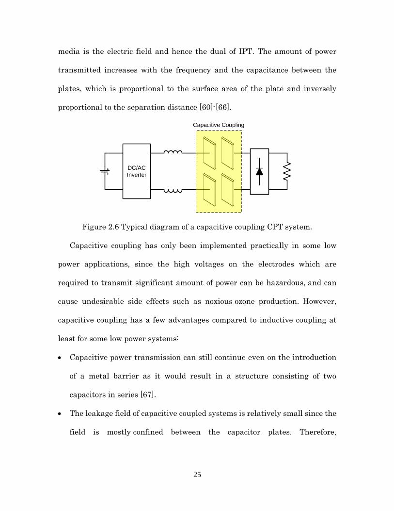
A block diagram of a capacitive coupled CPT system is given in Figure 2.6.
It can be considered as a pair of capacitors each consisting of two parallel plates
separated by a certain distance. It is based on the fact that when high
frequency AC voltage source is applied to the plates of the capacitor that are
placed close to each other, electric fields are generated and displacement
current keeps the current continuity. Therefore, in this case the energy carrier
25
media is the electric field and hence the dual of IPT. The amount of power
transmitted increases with the frequency and the capacitance between the
plates, which is proportional to the surface area of the plate and inversely
proportional to the separation distance [60]-[66].
DC/AC
Inverter
Capacitive Coupling
Figure 2.6 Typical diagram of a capacitive coupling CPT system.
Capacitive coupling has only been implemented practically in some low
power applications, since the high voltages on the electrodes which are
required to transmit significant amount of power can be hazardous, and can
cause undesirable side effects such as noxious ozone production. However,
capacitive coupling has a few advantages compared to inductive coupling at
least for some low power systems:
Capacitive power transmission can still continue even on the introduction
of a metal barrier as it would result in a structure consisting of two
capacitors in series [67].
The leakage field of capacitive coupled systems is relatively small since the
field is mostly confined between the capacitor plates. Therefore,

26
electromagnetic interference (EMI) and health-related concerns are
significantly reduced [68].
Alignment requirements between the primary and secondary plates are less
critical [65].
At high frequencies (MHz range), the efficiency of capacitive coupled
systems is higher than the efficiency of inductively coupled systems [69].
2.3.2 Microwave coupling
Power transfer through radio waves can be made more directional, which
ensures longer distance energy transmission with shorter wavelengths of
electromagnetic radiation, typically in the microwave range. Microwaves are
radio waves that have a spectrum range of 1-30 GHz. They are used widely in
many applications especially in communications. Unlike other radio waves,
microwaves can be transmitted in narrow beams allowing the transmitter to
focus its energy towards the receiver. In low power applications, such as mobile
cell phones, microwaves are generated or radiated from an antenna that is fed
with a high frequency current. The microwaves are then picked up by the
rectenna and converted back to an electric current. The simplified diagram of
a microwave power transfer system is illustrated in Figure 2.7 [70]-[72].
Microwave
Power
Source
Load
Antenna Rectenna
Microwave
Figure 2.7 An illustration of microwave power transfer.

27
The main obstacle that had to be overcome in order transfer high levels of
power using microwaves was the conversion of microwaves back to electricity.
When a microwave signal is picked by an antenna, an alternating current is
generated that has the same frequency of the microwave signal and is
proportional to the microwave’s signal power. Since all applications and
devices either operate at an AC voltage at 50 Hz or 60 Hz or from a constant
DC Voltage, the high frequency current generated by the microwave antenna
therefore has to be converted to a suitable voltage form. The rectenna which
was invented by W. C. Brown in 1963, is the key component of contactless
power transmission by microwave coupling [36]. It is a combination of a
rectifying circuit and an antenna that rectifies the high frequency current
generated by the microwave antenna into a DC voltage by using a bridge
rectifier. A simple rectenna can be constructed by placing a Schottky diode
between the antenna dipoles. Schottky diodes are employed because these have
the lowest voltage drop and highest switching speed and therefore lead to the
least amount of conduction and switching loss. Under experimental conditions,
rectenna conversion efficiencies exceeding 95% have been realized, and
microwave transfer efficiency was measured to be around 54% [49].
Since portable devices have small dimensions, the rectenna should also be
small in size. A small rectenna area leads to a low amount of received power,
which is a major disadvantage. Moreover, due to the health risks associated
with direct exposure to high energy microwaves, the use of this technology is

28
limited to applications where there is no danger of human exposure. On
account of these limitations, microwave power transfer is mainly suitable for
low power applications such as low power wireless sensors [73].
2.3.3 Laser coupling
The long distance contactless power transmission can be realized by
transferring electric energy from one location to another through laser light.
The basic idea is the same as solar power, where the sun shines on a PV cell
that converts the sunlight to energy. Here the laser beam of high intensity is
thrown from some specific distance to the load end. At the load end highly
efficient PV cells are utilized which receive the laser beam, energize laser light
and finally convert light energy in to electrical energy. The major differences
are that laser beam is much more intense than sunlight, it can be aimed at any
desired location, and it can deliver power 24 hours per day. Energy can be
transmitted through air or space, or through optical fibers, like
communications signals are sent nowadays, and it can be sent potentially as
far as the Moon [74]-[77].
Lasers generate phase-coherent electromagnetic radiation by the principle
of population inversion. The most efficient DC-to-laser converters are solid-
state laser diodes that are commercially employed in fiber optic and free-space
laser communication. Alternatively, direct solar pumping lasers involve the
concentration of solar energy before being injected into the laser medium. The
benefits of laser power beaming include [78]-[79]:

29
The focused beam leads to greater energy concentration at long distances.
The small size of the receiver allows easy integration into low profile
devices.
No radio-frequency (RF) interference to existing signal communication
approaches such as Wi-Fi and cell phones.
Unfortunately, there are certain disadvantages limit the applications of
laser [80]-[81]:
The imperfection of existing technologies leads to the loss of the most of
energy during the transformation of the laser beam into electric power. The
typical conversion efficiency from light to current is between 40-50% for a
single wavelength and 20-30% for the entire light spectrum. Before making
the method effective, more efficient solar cells must be developed.
Laser power beaming requires a line-of-sight between the transmitter and
receiver. Therefore, it is especially difficult to apply this technology in a
dynamic environment such as EV charging.
Light weather can reduce transmission efficiency and range, but heavy
weather (heavy rain or snow, or fog) can block transmission altogether
which causes up to 100% losses.
Laser radiation is harmful. Low power levels can easily blind humans and
animals. High power levels can kill living beings through localized spot
heating.

30
Laser power beaming technology has been mostly investigated in military
weapons and aerospace applications, and it is now being developed for
commercial and consumer electronic applications. Contactless energy transfer
systems using lasers for consumer applications have to comply with laser
safety requirements standardized under IEC 60825 [82]-[83].
2.4 State-of-the-art IPT systems
This section reviews the recent significant development and research in IPT
systems that can be found in the literatures which include technical papers,
scientific magazines, patents and industrial products. The power level for these
applications ranges from a few watts up to a few kilowatts.
2.4.1 Inductive charging
One of the first commercial applications for low power induction based
charger that has been in the market since the early 1990s is the electric
toothbrush. The electric toothbrush contains a battery that needs to be charged
regularly. This application is typically used in moist environment, and the
existence of an electric connector is a potential cause of domestic accidents.
Inductive charging allows enclosing and therefore fully insulating the wires. It
gives the advantage to protect the user against electric shocks due to apparent
contacts and to prevent short circuits that could damage electronics. The
development of an inductive based charger for electric toothbrush has begun
in the 1960s’. Several patents are filed regarding on how an electric toothbrush
can be charged contactlessly [84]-[86]. Figure 2.8(a) illustrates a schematic of

31
an early stage electric toothbrush with inductive charger. In these
applications, the primary winding and the inverter stage are placed in the
charger, which can be connected to the AC mains. The secondary winding and
the rectifier stage are placed inside the device, together with the battery to be
charged. The system generally includes a ferromagnetic core that increases the
coupling between the coils. The operating frequency is around 10 kHz or more,
and the transferred power is between 10 and 15 W. Similar IPT systems are
also integrated into electric shavers as shown in Figure 2.8(b) [87]. Efficiency
is not of major interest since the batteries charge at low power levels over a
long period of time.
(a) (b)
Figure 2.8 Schematic of (a) an electric toothbrush [85] and (b) an electric
shaver [87].
There are a lot of IPT researches dedicated to charging low power portable
devices since the early 2000s’. For example, the prototype of a small platform
allowing to recharge a mobile phone battery is proposed in [88]-[89]. A picture

32
of the prototype is given in Figure 2.9. The coreless transformer is made of
printed circuit board (PCB) coils that have to be precisely aligned to start the
charging process. The operating frequency is ranged between 920 and 980 kHz,
and the power transferred to the battery is 3.3 W, but the transformer has been
tested to transfer up to 24-W power. Another research team from the City
University of Hong Kong has also been investigating planar, low power
inductive battery chargers based on printed circuit board technology [90]-[96].
Their major contribution to the IPT technology is the design concept of
generating an even magnetic field across a large area. Therefore, many
problems from low power level to free positioning of the charging object have
been successfully solved. This charging pad concept was later used in
numerous applications for low power consumer electronics.
Figure 2.9 Prototype of a mobile phone battery charger [89].
More recently, many IPT systems for consumer electronic applications have
been marketed. The first company to start working on IPT system was
Splashpower in 2001 [97]-[98]. In order to avoid the receiving device from
blocking the vertical magnetic field, Splashpower developed a unique coil
design which enables the transmitting platform to transfer a horizontal field

33
in both X and Y direction. This enables the receiver to be insensitive to location
and rotation. However, with the introduction of many compact and low profile
devices, modern consumer electronic devices are more sensitive to the
thickness of the device. Therefore, the allowable extra cross sectional area on
the receiving device is almost non-existent. In addition, as one of the early
adopters of the technology the Splashpower system operates in tens of
kilohertz causing the system to be more inefficient than current solutions
which operate at hundreds of kilohertz. Splashpower was acquired by Fulton
Innovation also known as eCoupled in 2008 [99].
eCoupled’s wireless power technology was a by-product of its parent
company Alticor’s eSpring water purifier [100]. Approximately 15 years ago
engineers at eCoupled were trying to prevent corrosion and electrical shock
hazard to the ultraviolet lamp, and in the end they developed an IPT system
to solve this issue. The first IPT table developed by eCoupled allows
transferring energy to multiple but fixed devices [101]. This application has
the ability to communicate with the devices which allows adaptively
transferring the exact amount of power required by each load on the platform.
Although the cost of the system is reasonable to the unique water purifier, it
is considered to be high for cost sensitive consumer electronics which have very
low profit margin. However, eCoupled has successfully demonstrated a power
delivery up to 1000 W grilling a piece of steak on a George Foreman grill as

34
well as powering a 2000-W food processor at the 2008 international Consumer
Electronics Show (CES) [102].
At CES 2009, Palm Inc. announced their new Pre smartphone would
provide an optional inductive charger accessory called the “Touchstone” [103].
The charger came with a required special back cover that became standard on
the following Pre Plus model announced at CES 2010. The user would place
the phone on a wireless charging pad and the phone would charge as if it was
charged via a cable. Figure 2.10(a) demonstrates the Touchstone charging dock
and Figure 2.10(b) shows a teardown picture of it [104]. Figure 2.10(c) shows
the receiver that is located in the back cover of the smartphone [105]. It can be
noticed that magnets are used to align the receiver with the transmitter in
order to ensure that a high coupling coefficient is achieved. Palm Inc. was
acquired by HP in 2010, and the later HP Touchpad tablet came up with a
built-in coil and inductive charging dock [106].
(a) (b) (c)
Figure 2.10 Inductive charging kit from Palm Inc.: (a) Touchstone charging
dock [104], (b) a teardown view of the charger [104], (c) the receiver located in
the back cover of Palm Pre smartphone [105].

35
Other companies are present on this market with similar platforms and
applications, such as Powermat from Duracell [107], WiPower from Qualcomm
[108], Jolt Charger from Mojo Mobility [109], VÜ wireless charger from TYLT
[110], and so on. The common features to these applications are the low power
devices that they can supply, the predetermined placement of the devices on
the platform and the integrated intelligence that detects and recognizes the
devices.
IPT systems can also be applied to high power level applications such as EV
battery charging. Transportation sector is the largest consumer of fossil fuel
worldwide and consequently major factor in reducing fossil fuel demand. Due
to the limited availability of fossil fuel and the demand to reduce the emissions
in transportation sector, the development of EVs worldwide over the past
decade has been initiated. Therefore, new methods and techniques are being
researched on how to charge the batteries on board the vehicle. Currently,
plug-in connections are used in EVs for charging where the user inserts the
plug into the receptacle of the vehicle to charge the batteries. The major
drawback of using cable and connector type is the risk of electrocution
especially in wet and hostile environments since it delivers 2 - 3 times more
power than standard plugs at home. Long wires would cause a tripping hazard
and are also aesthetically poor. In harsh climate locations where have snow
and ice, the plug-in charge point may become frozen onto the vehicle.
Therefore, in order to eliminate the above disadvantages, the inductive

36
charging has been developed which can charge the batteries contactlessly
[111]-[112].
The beginning of IPT system for EV charging can be dated back to 1894
when Hutin and LeBlanc submitted a patent which describes a transformer
system for electric railways [113]. Although the system is named as
“transformer”, it basically represents an IPT system for street vehicle
supplying. It consists of a single wire primary track with 2 kHz excitation AC
current and multiple resonant receivers at the secondary side. Ferromagnetic
material and a suspension system that lowers the receiver were proposed to
increase mutual coupling between the primary track and the receiver.
Although the proposed topology has some similarities to modern solutions, its
practical implementation was not successful.
A project called Partners for Advanced Transit and Highways (PATH) was
conducted at the University of California, Berkeley in the early 1990s’ [114].
The goal of the project was to validate the concept of a roadway powered
electric vehicle. A 60-kW, 35-passanger bus was selected as the test vehicle.
The complete infrastructure was built for a 213-meter long track with two
powered sections with total length of 120 meters. A bipolar primary track
which was supplied with 1200-A, 400-Hz AC current was used. The receiver
had an area of 4.3 m2, and a 7.6-cm gap distance from the primary track was
used. The obtained efficiency was around 60%. The results of the project have

37
proved the considerable potential of roadway vehicle charging, but the very low
operating frequency applied has been identified as a serious limiting factor.
The Magne Charge (Fig. 2.21) was the first commercially available IPT
system to charge the batteries of EVs. The system was developed by Delco
Electronics to be used on battery powered vehicles formerly by General Motors,
such as the EV1, Chevy S10 EV, and so on. It is still equipped by a few hundred
first generation Toyota RAV4 EVs. As Figure 2.11 shows, the primary charging
paddle of the Magne Charge inductively coupled charger was sealed in epoxy
as was the secondary. The paddle inserted into the center of the secondary coil
permitted charging of the EV1 without any contacts or connectors at either 6.6
kW or 50 kW. The reported efficiency for the 6.6-kW Magne Charge system is
around 86% excluding the rectification stage. Magne Charge support was
discontinued by General Motors in 2002, after the California Air Resources
Board settled on a conductive charging interface (SAE J1772) for EVs in
California in June, 2001 [115]-[117].
(a) (b)
Figure 2.11 The Magne Charge system: (a) the charging stating, (b) the
primary charging paddle [116].

38
At the same time, a research group at the University of Auckland, New
Zealand have also focused their attention on EV inductive charging. They have
investigated various aspects of the IPT including topologies of the primary
resonant inverter, tuning networks of the primary and secondary circuits, the
optimal control of the receiver, the multi-phase design of the primary track,
the bifurcation phenomenon, and many others. Supported by this technique,
some early achievements have been made by Conductix-Wampfler, such as the
20-kW charging bay for 5 golf buses in New Zealand during 1997 to 2007 and
the 60-kW wireless charging urban bus fleets in Genoa and Turin, Italy in 2002
and 2003. The University owned company HaloIPT released a 3-kW evaluation
kits in 2010, which could achieve 85% overall efficiency through 180-mm air
gap. It was acquired by Qualcomm in 2011. In the same year, Qualcomm
announced a pre-commercial trial in London, using similar kits but aiming to
the mass consumer adoption of this technology [118]-[122].
Witricity, a Massachusetts Institute of Technology (MIT) spinoff,
cooperated with Delphi Automotive and Toyota to develop commercial
inductive charging system for EV. Figure 2.12 illustrates the components of
the WiT-3300 deployment kit from Witricity. The claimed grid-to-battery peak
efficiency for the 3.3-kW system is around 90% with up to 180-mm gap between
the primary and secondary windings [123]-[125].

39
Figure 2.12 The WiT-3300 deployment kit from WiTricity [133].
ORNL, mostly focusing coils design, announced two IPT prototypes for EV
in 2012. The 7-kW prototype has two identical 800-mm diameter coils with Litz
wire and soft ferrite plates could reach around 93% coil-to-coil efficiency. The
2-kW prototype, using a different 330-mm diameter coil design, was tested on
a GEM EV powered by 72-V lead-acid battery. Experiments have been done in
both stationary and dynamic charging applications. The highest tested coil-to-
coil efficiency is around 91% with an air gap of 75 mm [126]-[129].
Using the similar technology, Evatran began development of Plugless
Power, which is claimed to be the world’s first hands-free, plugless, proximity
inductive charging system for EVs in 2009. It has an over 90% grid-to-battery
efficiency as claimed for the 3.3-kW system with 100-mm gap distance. With
the participation of the local municipality and quite a few businesses, field
trials were started in March 2010. It has already been successfully installed in
Nissan Leaf or Chevrolet Volt. The first system was sold to Google in 2011 for
employee use at the Mountain View campus. At the end of 2012, it announced
a trial called Apollo Launch Program, aiming to the integration of this
technology to current on-sale EVs across the United States. Evatran began

40
selling their Plugless L2 Wireless charging system to the public in 2014 [130]-
[132].
Another breakthrough in the IPT technology, especially in the area of EV
dynamic charging, were results and knowledge obtained from the On-Line
Electric Vehicle (OLEV) project conducted by the Korea Advanced Institute of
Science and Technology (KAIST) in South Korea. The high price, high weight,
and limited range of batteries for EVs motivated researchers to develop a
roadway charging system that could reduce the required amount of batteries
by up to 80%. As shown in Figure 2.13, the OLEV system consists of having
two parallel conductors in segments, which are turned on only when a bus is
driving over them. In addition, primary power tracks can be installed at part
of the bus route and where there are none, the battery suffices. Three
generations of OLEV systems have been developed with three different level
vehicles tested accordingly: a light golf cart for the first generation, a bus for
the second, and a sport utility vehicle (SUV) for the third. In each generation,
a different configuration of ferromagnetic material and a different track layout
have been designed. For the second and third generation, 60-kW power
transfer for the buses and 20-kW for the SUVs achieve efficiency of 70% and
83%, respectively. The allowable vertical distance and lateral misalignment
range up to 16 cm and 20 cm, respectively [133]-[136].

41
Figure 2.13 OLEV system from KAIST [133].
Another company which also works to make inductive charging while
driving a feasible option is PRIMOVE, the e-mobility unit within Bombardier.
PRIMOVE doesn’t only work for inductive charging of buses, but for cars and
trams as well. For buses the scheduled stops are ideal locations for charging
the batteries and can be distributed among the stops to minimize the need for
wayside infrastructure. If there is an abrupt slope along the bus route,
additional dynamic charging sections can be installed to provide extra energy
so as to avoid the battery losing too much power. Using this solution for trams
provides an extra bonus since no cable wires are needed and therefore would
not cause any visual pollution. Just like with buses, a mix of static and dynamic
charging works best, and minimizes the need for batteries and roadside
infrastructure. PRIMOVE’s solution employs a three-phase system which is
divided into segments, to avoid unnecessary magnetic field around the roads
and maximize its efficiency. An antenna is utilized to communicate with the
road so that only the segments directly under the vehicle are on. There is a
control unit in the vehicle which decides how to best utilize the power, for
42
charging of the batteries, for propulsion or for both. One successful
demonstrator already runs in Berlin and development projects to supply heavy
trucks at highways are going on [137]-[139].
A very important step toward broader acceptance of any new technology is
the standardization of circuit topologies, design methods, and verification
procedures. Recognizing the necessity of IPT systems standards for low power
consumer electronics chargers, three standards were developed in the past few
years. A consortium named the Wireless Power Consortium (WPC) was
established in 2008 by several electronics manufacturers that aimed to create
a universal wireless power transmission standard that would allow devices to
be charged by chargers built by different manufactures [140]. The WPC
standard is referred to as “Qi” (pronounced “chee”) and has the logo shown in
Figure 2.14(a). Power Matters Alliance (PMA) is another industry organization
whose objective is to advance a suite of standards and protocols for IPT [141].
Founded by Procter & Gamble and Powermat Technologies in March 2012,
PMA is networking technology companies so as to guarantee consumers
interoperable devices which employ wireless power technology. Another
interface standard “Rezence” has been developed by the Alliance for Wireless
Power (A4WP) in early 2012 [142]. With the magnetic resonance technology,
A4WP is aiming to improve the power range and spatial freedom when
charging mobile devices. In January 2015, A4WP and PMA announced that
the two organizations will merge into a new organization [143]. Table 2-1 helps

43
clarify the differences between these three main low power inductive charging
standards [144]-[145].
(a) (b) (c)
Figure 2.14 Low power wireless charging standards: (a) WPC [140], (b) PMA
[141], (c) A4WP [142].
Table 2-1 Comparison of low power wireless charging standards [144]-
[145]
Standard WPC PMA A4WP
Founders Various Duracell-
Powermat Samsung/Qualcomm
Key Supporters Verizon, Nokia AT&T,
Starbucks WiTricity, Intel
Members 212 70 140
Products >700 10 0
Phones
Integrated >70 0 0
Market Phone/Industry Phone/Tablet Phone/Tablet
Power Class 5 W - 2.4 kW 5 - 20 W 5 - 20 W (-90 W)
Power
Frequency 100 - 205 kHz 277 - 357 kHz 6.78 MHz
Communication
Frequency 100 - 205 kHz 277 - 357 kHz 2.4 GHz, ISM Band
Additionally, plenty of governmental organizations, vehicle manufacturers,
IPT suppliers and infrastructure companies have agreed recently to develop a
new standard SAE J2954 for standardization of IPT-based chargers for EVs.

44
In November 2013, the SAE J2954 Task Force announced that an agreement
was reached on WPT common operating frequency that would guarantee
interoperability. The WPT low frequency band centers at 85 kHz, but ranges
from 81.38-90 kHz. This frequency band is available not only in the U.S. and
also internationally. In addition, the SAE J2954 Task Force has also
determined three power levels for light duty vehicles, WPT 1, 2 and 3. These
limits are defined by the maximum input WPT power rating at 3.7 kW, 7.7 kW,
and 22 kW, respectively. The SAE J2954 Task Force is currently working on
completing the remaining interoperability topics, such as the minimum
coupling coefficient, alignment range, communication method, coil geometry,
and so on [146].
2.4.2 Induction heating
Induction heating is another form of transferring energy contactlessly via
inductive coupling [147]-[148]. It is the process of heating an electrically
conductive metal object by electromagnetic induction, through heat produced
in the object by eddy currents. An induction heater contains an electromagnet,
and an electronic oscillator which conducts a high frequency AC current
through the electromagnet. The high frequency alternating magnetic field
penetrates the object, generating eddy currents inside the conductor. The eddy
currents flowing through the internal resistance of the metal object heat it
through Joule effect. In ferromagnetic materials like iron, heat could also be
generated due to magnetic hysteresis losses. The frequency of AC current to be

45
used depends on the object size, type of material, coupling between the
induction coil and the object to be heated, and the magnetic field penetration
depth.
A major advantage of the induction heating process is that the heat is
produced inside the metal object itself, rather than by an external heat source
through heat conduction. Therefore objects can be heated very rapidly.
Furthermore, no direct external contact is necessary, which can be important
where contamination is a concern. Induction heating technology is utilized in
many residential and industrial applications as shown below:
Induction cooking
As shown in Figure 2.15, the typical setup of an induction cooking system
is made up of: the high frequency resonant inverter generating the AC current;
the coil, usually a flat disc with solid or Litz wire as conductors; the thermal
insulator, placed between the pan and the coil to avoid the coil to be damaged
by heat; the ferrites, which are used to shape appropriately the magnetic field;
the cooking vessel [149]-[150]. When a high frequency alternating current
generated by the inverter flows through the induction coil, a magnetic field of
the same frequency is produced. If the pan is placed on the hob, the magnetic
field generates eddy current in the bottom part of the pan. The internal
resistance of the pan generates heat to be dissipated, following the Joule effect.
For induction cooking, the heat is generated in the cooking pan directly and
is then transferred to the pan's contents. No heat is dissipated outside the pot

46
during the electrical-heat transfer process. Therefore, the thermal efficiency of
an induction cooker is significantly higher than that of other cooking methods
such as gas or an ordinary electric cooker. In addition, induction cooker
provides rapid heating and instant adjustment on energy flow. Moreover,
induction cookers are safer to use compared to conventional cookers because
there is no open flame and the element itself reaches only the temperature of
the cooking vessel. Last but not the least, induction cookers are easier to clean
since the cooking surface is flat and smooth [151]-[153].
High Frequency Inverter
Thermal Insulator
Pan Eddy Current
Heating Coil
Magnetic Flux
Figure 2.15 Principle of induction cooking [150].
However, in spite of that many merits, conventional induction cooking
systems still have some disadvantages. Firstly, traditional induction cooking
systems have been designed to operate with cooking vessels made from
magnetic materials, mainly cast iron or ferromagnetic stainless steel, which
has a high resistivity and relative permeability. Secondly, an induction cooker
must match the shape of the pan, so the usual flat-top cooker works well only
with flat-bottom pans. Furthermore, since the electronics within an induction

47
cooker must not be heated excessively during operation, the units usually
employ fan-cooled heat sinks which are attached to the components requiring
cooling and proper flow channels and venting for the heated air, hence the
weight of the induction heating cooker system is increased [154]-[155].
Induction furnace
An induction furnace utilizes magnetic induction to heat metal to its
melting point. Once melted, the high frequency magnetic field could also be
utilized to stir the hot metal, which is helpful in ensuring that alloying
additions are completely mixed into the melt. Most induction furnaces
comprise a tube of water-cooled copper rings surrounding a container
of refractory material. Induction furnace is better compared to most other
means of metal melting because it is a clean, energy-efficient and well-
controllable melting process. Most modern foundries utilize this type of
furnace, and nowadays more iron foundries are also replacing cupola furnaces
with induction furnaces to melt cast iron, because the former method lead to
lots of dust and other pollutant emissions. Induction furnace capacities range
from one kilogram to a hundred tons and are utilized to melt iron, steel, copper,
aluminum, and precious metals. Because no arc or combustion is utilized, the
temperature of the material would not be higher than required to melt it, which
can prevent the loss of valuable alloying elements. The major disadvantages to
induction furnace usage in a foundry include the lack of refining capacity,

48
charge materials need to be clean of oxidation products, and some alloying
elements might be lost due to oxidation process [156].
Induction welding
A similar, smaller scale process is employed for induction welding. Plastics
can also be welded by magnetic induction, if they are doped with either
ferromagnetic ceramics or metallic particles. Seams of tubes could be welded
using this process. Currents induced in a tube flow through the open seam and
heat the edges leading to a temperature high enough for welding. At this time
the seam edges are forced together hence the seam is welded [157].
2.4.3 Biomedical implants
Biomedical implants are gaining prominence and are expected to play an
important role in saving and extending human lives, due to their ability to
monitor, stimulate and regulate vital internal organs, and also communicate
with the external host about the health condition of the these internal organs.
They have been applied in a wide range of areas, including pacemakers,
cochlear hearing implants, physiological monitoring devices, drug infusion
pumps, artificial hearts, and nerve stimulation devices [158]-[159].
The power requirement of these devices depends on the specific application,
and the typical range is from microwatts to milliwatts. Traditional operation
of most biomedical implants relies heavily on continuous power supply from
batteries which are problematic because they eventually have to be
contactlessly recharged or replaced requiring invasive surgery. Battery

49
powered biomedical implants also limit the realizable applications due to the
size and lifetime. A promising solution for this limitation is the use of IPT
systems that can avoid transcutaneous wiring and the replacement of
batteries. When developing IPT systems for biomedical implants, the power
levels are strictly regulated. Too little power can cause malfunction of the
device, while extra power can lead to excessive heat or damage in the
surrounding tissues. This power restriction requires the design of low power
transmitters that can contactlessly transfer power with high efficiency.
Displayed in Figure 2.16 are examples of previously published IPT based
biomedical implants [161]-[169].
(a) (b)
(c)
Figure 2.16 IPT based biomedical implants: (a) cochlear hearing implant
[163], (b) drug infusion pump [166], (c) nerve stimulation device [169].

50
2.4.4 Radio-frequency identification
Radio-frequency identification (RFID) is a fast developing technology with
a wide range of applications in various areas. RFID uses electromagnetic fields
to transfer the data stored in a device, for the purpose of automatically
identifying and tracking tags that are attached to objects. A RFID system has
two main components, a reader and a tag. The reader is also referred to as the
interrogator which sends a signal to the tag and read its response, while the
tag is attached to the objects to be identified [170].
RFID tags are categorized as active, passive or battery-assisted passive.
Active tags are autonomous and have their own power source, usually using
an on-board battery. Active tags transmit a stronger signal, and can achieve a
larger read range (20 - 100 m) and higher data rates. Active tags operate at
higher frequencies - normally 455 MHz, 2.45 GHz or 5.8 GHz depending on the
application and memory requirements. However, their high cost and
considerable size are major shortcomings. When the required read range is
small and data rate is not critical passive tags offer a desirable alternative.
This type of tag doesn’t have an internal battery and is powered from the
transmitter’s radiated field. Data is transferred between the reader and the
tag by means of load modulation techniques where the reflected impedance of
the tag seen by the reader is modulated by the tag to represent data. Usually
passive tags consist of low power CMOS devices, very compact and
inexpensive. The process by which a passive tag is powered is inductive near

51
field coupling and typical read range is about one meter. In battery-assisted
passive tags, power is obtained from an internal battery in the tag, but the
transmission of data is done in a similar manner to that of passive tags [171]-
[173].
RFID tags can be embedded in numerous objects due to their small size and
low manufacturing cost. RFID tags are currently being attached to identity
cards, passports and travel documents for personal identification purposes.
They are also attached to objects and utilized to track and manage inventory,
assets, etc. In addition, implantable RFID tags have been used for livestock
tracking for many years which help bridge the gap between the RFID and
embedded sensor domain. A recent but increasing development of this
technology which arouses great interest is the use of RFID in humans as a
method of accessing and tracking medical records in hospitalized or
incapacitated patients. Efficiency is typically low for an RFID system, however
it is not of major interest since the system usually operates at very low power
levels [174]-[176].
2.5 Summary
CPT is not a new concept. It is based on the Ampère’s circuital law and
Faraday's law of induction. Maxwell developed the classical electromagnetic
theory based on the observations, experiments and equations, while Tesla first
demonstrated contactless power transmission in 1893. Several approaches
were investigated throughout the twentieth century to transfer power

52
contactlessly between two distant locations. The research in microwave and
laser based CPT was of high interest during the 1970s and 1980s. Several proof
of concept experiments were conducted and concluded that microwave based
CPT has the potential to transfer large amounts of energy over several
kilometers. However, the cost of building such a system can be significantly
high.
Induction coupling based CPT or IPT has gained a lot attention recently
due to the increasing dependence on battery-powered applications ranging
from EVs to mobile devices and biomedical implants. Several standards, such
as the Qi, PMA and A4WP standards, have been developed to allow for a better
integration between various low power charging devices. While many
companies also work together to develop a new standard SAE J2954 for
standardization of IPT-based chargers for EVs.
Various applications and research fields for IPT system have been
presented in this chapter. By reviewing several commercial products and their
related patents, it can be noticed that the two important issues for an IPT
system, including its overall efficiency and the distance as well as the
alignment between the transmitter and the receiver, are usually overlooked or
not mentioned. While in research papers, only the power tranfer efficiency from
the primary winding to the secondary winding is mentioned.
It is noticed that the major target in recent publications was to boost the
efficiency of an IPT system by reducing any losses or increasing the amount of

53
power that is available to the load. The research focus has now shifted towards
creating novel electric circuit topologies and methods to increase the ability of
an IPT system to transfer higher power levels, as well as to reduce the losses
owing to the electronic switches employed in the inversion and rectification
processes and the conduction losses in the passive components. However, many
realistic design considerations that may help improve the feasibility of the IPT
systems are neglected.

54
Chapter 3 Analytical Model of Inductive Power Transfer Systems
3.1 Introduction
The front-end PFC stage technology is relatively mature, hence the
remaining DC-DC stage as shown in Figure 3.1 are of more interest in this
dissertation. The current flowing in the primary coil of a LCT has to be
alternating in order to generate an alternating magnetic field to induce a
voltage in the secondary coil. Producing an AC current from a DC voltage
requires the use of a high frequency DC-AC resonant inverter. The output AC-
DC rectifier converts the AC voltage received by the secondary coil to a DC
voltage for the load. The additional DC-DC converter is also eliminated with
accurate control in the aforementioned converters to reduce the cost and size
for the receiver side.
There are several types and classes of switched-mode DC-AC inverters and
AC-DC rectifiers can be employed in the IPT system. Their performance and
characteristics such as device stress, device count, control complexity, and
suitable applications will be discussed in this chapter.
As the essential component in the IPT system, the principle of operation of
LCT will be analyzed from a circuit point of view. Various electric circuit
models is used to analyze the LCT and calculate the induced voltages and
currents across the transmitting and receiving coils. Numerous compensation
network configurations will be presented and their corresponding advantages
and disadvantages will be introduced.
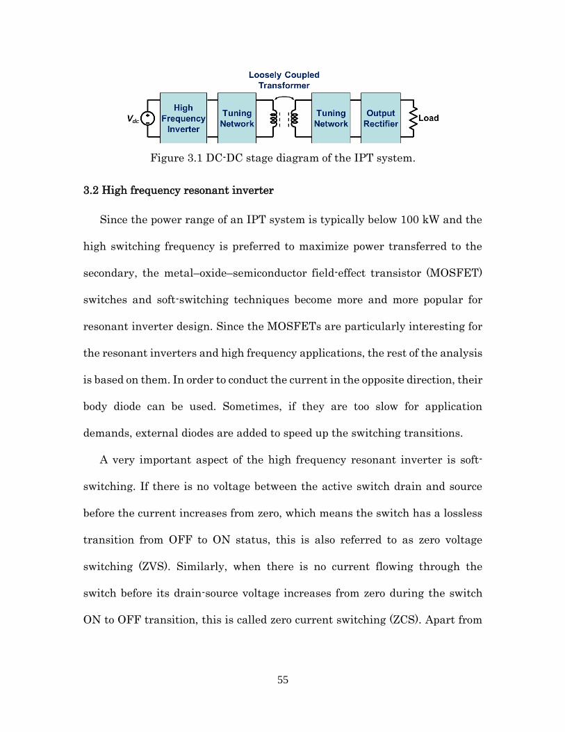
55
Figure 3.1 DC-DC stage diagram of the IPT system.
3.2 High frequency resonant inverter
Since the power range of an IPT system is typically below 100 kW and the
high switching frequency is preferred to maximize power transferred to the
secondary, the metal–oxide–semiconductor field-effect transistor (MOSFET)
switches and soft-switching techniques become more and more popular for
resonant inverter design. Since the MOSFETs are particularly interesting for
the resonant inverters and high frequency applications, the rest of the analysis
is based on them. In order to conduct the current in the opposite direction, their
body diode can be used. Sometimes, if they are too slow for application
demands, external diodes are added to speed up the switching transitions.
A very important aspect of the high frequency resonant inverter is soft-
switching. If there is no voltage between the active switch drain and source
before the current increases from zero, which means the switch has a lossless
transition from OFF to ON status, this is also referred to as zero voltage
switching (ZVS). Similarly, when there is no current flowing through the
switch before its drain-source voltage increases from zero during the switch
ON to OFF transition, this is called zero current switching (ZCS). Apart from

56
the losses in the active switches, diode reverse recovery loss should also be
minimized.
In this section, three types of mainly used high frequency DC-AC resonant
inverter will be introduced: full bridge inverter, half bridge inverter, and class-
E inverter. Individual operation principle and waveform will be analyzed,
switch current and voltage stress will be calculated, device count will be
compared, and suitable application power range will be identified.
3.2.1 Full bridge inverter
Figure 3.2 shows the circuit diagram of a high frequency full bridge
inverter. The single-phase inverter is supplied by a DC input voltage Vdc
created by the active PFC circuit. Figure 3.3(a) and Figure 3.3(b) illustrate the
gate signal for Q1/Q3 and Q2/Q4, respectively. It is obvious that each active
switch conducts almost 50% of the switching period, Ts, in order to obtain
maximum fundamental output voltage Vp. It is well know that the turn-on and
turn-off transitions of active switches take some time. Therefore, two switches
in the same branch of a full bridge inverter must not start their transitions at
the same time, since this situation would cause a short circuit condition over
the DC bus. To avoid this situation, a small time interval called dead time Tdead,
or a blank interval, is inserted between the initialization of the turn-off
transition of one switch and turn-on transition of the other.

57
Q1
Q2 Q3
Q4
Vdc vp
ipVdc
Vp
Figure 3.2 Full bridge inverter diagram.
G1, G3
G2, G4
vp+Vdc
-Vdc
(a)
(b)
(c)
Ts
Tdead
vds1, vds3 (d)+Vdc
Figure 3.3 Full bridge inverter waveforms: (a) Q1 and Q3 gate signals, (b) Q2
and Q4 gate signals, (c) inverter output voltage vp, (d) vds of Q1 and Q3.

58
The waveform for the full bridge inverter output voltage vp is depicted in
Figure 3.3(c). The fundamental inverter output voltage amplitude Vp can be
calculated as
4
p dcV V (3.1)
Figure 3.3(d) indicates that in the full bridge inverter, the voltage stress for
each device is equal to the DC bus voltage Vdc, and the current stress for each
device can be calculated as
_rms _
1
2MOS p rmsI I (3.2)
Where Ip_rms represents the root mean square (RMS) value of the full bridge
inverter output current.
3.2.2 Half bridge inverter
Figure 3.4 shows the circuit diagram of a high frequency half bridge
inverter. Instead of employing four active switches as in the full bridge
topology, two active switches are required and two DC bus capacitors are
utilized in the half bridge inverter. Each capacitor holds half of the DC input
voltage Vdc created by the active PFC circuit. Figure 3.5(a) and Figure 3.5(b)
illustrate the gate signal for Q1 and Q2, respectively. Similar to the operation
principle in full bridge inverter, each active switch conducts almost 50% of the
switching period Ts, with a small dead time Tdead inserted between the
initialization of the turn-off transition of one switch and turn-on transition of
the other to avoid shoot-through issue and to ensure ZVS operation.

59
Q1
Q2
Vdc vp
ipVdc/2
VpC1
C2
Figure 3.4 Half bridge inverter diagram.
G1
G2
vp
+Vdc/2
-Vdc/2
(a)
(b)
(c)
Ts
Tdead
vds1 (d)+Vdc
Figure 3.5 Half bridge inverter waveforms: (a) Q1 gate signals, (b) Q2 gate
signals, (c) inverter output voltage vp, (d) vds of Q1.
The waveform for the half bridge inverter output voltage vp is depicted in
Figure 3.5(c). The fundamental inverter output voltage amplitude Vp can be
calculated as

60
2
p dcV V (3.3)
Figure 3.5(d) indicates that in the half bridge inverter, the voltage stress
for each device is equal to the DC bus voltage Vdc, and the current stress for
each device can be calculated as
_rms _
1
2MOS p rmsI I (3.4)
3.2.3 Class-E inverter
VdcQ
Lf
Cs
Cp
vds
ipLp
Figure 3.6 Class-E inverter diagram.
0.0019975 0.001998 0.0019985 0.001999 0.0019995 0.002
Time (s)
0
-20
20
40
60
80
100
Vds
G
vds
ILf
Ts
(a)
(b)
(c)
Figure 3.7 Class-E inverter waveforms: (a) inverter input current, (b) Q gate
signals, (c) vds of Q.
The class-E inverter was first introduced in 1975 [177]. The basic schematic
of the class-E inverter is shown in Figure 3.6. This circuit is supplied by a DC

61
bus voltage Vdc. Only one low side active switch Q with its source terminal
grounded is employed hence simplifying the gate driving circuitry. The circuit
also contains four passive elements. Inductance Lf is referred to as the DC-feed
inductance. If the DC-feed inductance is large enough, the input current ILf of
the inverter is approximately constant, which is equal to its DC component as
shown in Figure 3.7(a). Capacitor Cs is referred to as the shunt capacitor.
Capacitor Cp and inductor Lp form a series resonant network. If the class-E
inverter is used in the primary of an IPT system, primary self inductance of
the LCT can serve as the inductor Lp and primary compensation capacitor can
serve as the resonant capacitor Cp.
The MOSFET Q is driven by the driving signal as shown in Figure 3.7(b).
When the switch is ON, the voltage across the switch is approximately zero
and the switch current flows through the MOSFET. During the switch OFF
interval, the difference of currents through the DC-feed inductance and the
resonant filter flows through the shunt capacitor. The current through the
shunt capacitor produces the pulse shape switch voltage as shown in Figure
3.7(c). Not only can the Class E inverter operate at ZVS, the voltage across the
switch has a zero slope at the instant at which it is turned ON. This is referred
to as zero derivative switching (ZDS). ZVS prevents the dissipation of the
energy stored by the shunt capacitor when it turns on, and ZDS makes the
circuit robust in the face of variations in the components, frequency, and
switching instants [178]-[179]. Due to this feature, the class-E inverter

62
achieves high power conversion efficiency at high frequencies. Assuming the
switch is turned ON at t = 0, the class-E inverter ZVS/ZDS conditions can be
expressed as
(0) 0dsv (3.5)
0
( )0ds
t
dv t
dt (3.6)
When a class-E inverter operates in a nominal condition with a 50% duty
cycle, the maximum voltage on the MOSFET drain terminal is depicted in the
following equation under a supply voltage Vdc [180]:
_ max
2ds dcV V (3.7)
where represents the phase of the class-E inverter output current ip with
reference to the gating signal. Under 50% duty cycle operation condition, can
be calculated as
2arctan 0.5669 rad 32.48 (3.8)
Equation (3.7) then becomes
_ max
3.562ds dcV V (3.9)
Similarly, the RMS value of primary and MOSFET current can be
calculated as
2
_rms
41.317
2 2p dc dcI I I (3.10)
2
_rms
281.538
4MOS dc dcI I I (3.11)

63
3.2.4 Resonant inverter comparison
This section presented a brief review of three commonly used high
frequency resonant DC-AC inverters in the IPT systems.
The full bridge inverter has the highest component count, hence increase
the overall cost of the system. The device voltage is equal to the bus voltage
and current RMS value is equal to 1 √2⁄ of the inverter output RMS current.
The inverter output voltage vp swings between -Vdc and +Vdc, hence the
inverter output current ip is moderate compared to that in the half bridge
inverter. Therefore, the full bridge inverter is suitable for high power (>500 W)
operation conditions.
The half bridge inverter consists of two active switches, resulting in modest
system cost. Similar to the full bridge inverter, the device voltage is equal to
the bus voltage and current RMS value is equal to 1 √2⁄ of the inverter output
RMS current. However, the inverter output voltage vp swings between -Vdc/2
and +Vdc/2, hence the inverter output current ip is twice as that in the half
bridge inverter. Therefore, the conduction loss is higher compared to that for a
full bridge inverter with same requirement. This feature renders the half
bridge inverter feasible for medium power (<500 W) applications, especially
when the required DC output voltage is much lower than the given DC input
voltage.
The class-E inverter has the fewest active switch count, hence lower the
system cost significantly. Due to its ZVS/ZDS feature, the MOSFET can be

64
softly turned ON and that leads to less switching losses allowing the inverter
to operate efficiently with very high frequency (MHz region). However, owing
to its resonant operation principle, the device voltage and current stress are
relatively higher than that for a full bridge or half bridge inverter, which
threatens the reliability of the device. In order to ensure the circuit reliability
when implemented in an IPT system where the load and coupling coefficient
are always changing, a switch with a maximum voltage rating of at least four
times the input voltage may be required. Therefore, the class-E inverter is only
suitable for low power and low voltage IPT systems [181]-[185].
Table 3-1 lists all the inverters that have been discussed in this section and
provides a comparison between them in terms of switch count, device voltage
and current stress, inverter output voltage and current, and power output
capability.
Table 3-1 Summary and comparison between the resonant inverters
Inverter Full bridge Half bridge Class E
Switch count 4 2 1
Vds_max Vdc Vdc 3.562·Vdc
IMOS_rms /4·Idc /2·Idc 1.538·Idc
vp_max Vdc 1/2·Vdc 3.562·Vdc
ip_rms π 2√2⁄ ·Idc π √2⁄ ·Idc 1.317·Idc
Power output
capability High Medium Low

65
3.3 Output rectifier
The output induced in the LCT secondary coil is always an AC voltage,
while most applications nowadays are consider DC loads which are either
represented by a resistor or a current sink. To deliver the received power to a
DC load requires the use of an AC-DC rectifier. The AC-DC rectification
circuitry is extensively studied and well described in literature. The main
losses that occur in the rectifiers are caused by the forward voltage drop of the
rectifying diodes and their switching losses. Synchronous rectification
technique which replaces diodes with MOSFETs can improve the overall
efficiency in IPT systems. However timing and control of the active switches is
nontrivial especially at high resonant frequencies.
The majority of the output AC-DC rectifier that have been employed in
recent publications about the IPT systems include full bridge rectifier, half
bridge rectifier (also referred to as the voltage doubler), and center-tapped full-
wave rectifier (also referred to as the current doubler). In this section, a brief
discussion will be provided on these three types of AC-DC rectifiers with the
assumption that the AC voltage to be rectified is pure sinusoidal. The operation
principles and waveforms will be analyzed, device current and voltage stress
will be calculated, device count will be compared, power conversion efficiency
will be evaluated, and suitable application power range will be identified.

66
3.3.1 Full bridge rectifier
The full bridge rectifier, also referred as full-wave bridge rectifier, employs
four individual rectifying diodes connected in a closed loop “bridge”
configuration to generate the desired output. Compared to half-wave rectifier,
a full bridge rectifier not only transfers the positive portion of the AC voltage
signal, but also converts the negative portion into a positive voltage.
As shown in Figure 3.8, the four diodes D1 to D4 are arranged in series pairs
with only two diodes conducting current during each half cycle. During the
positive half cycle, diodes D1 and D3 are conducting the current while
diodes D2 and D4 are reverse biased and the current flows through the load.
During the negative half cycle, diodes D2 and D4 are conducting the current,
but diodes D1 and D3 turn OFF since they are now reverse biased. The current
flowing through the load is the same direction as before. Because the current
flowing through the load is unidirectional, the voltage developed across the
load is also unidirectional hence the AC to DC conversion is achieved.
is
RL
Io
VoVs
vs Co
+
Vo
-
D1
D2 D3
D4
Figure 3.8 Full bridge rectifier diagram.
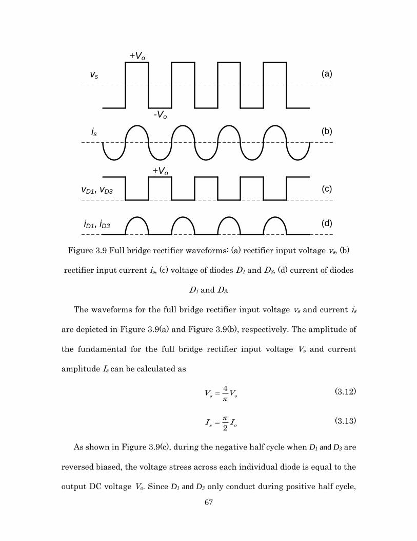
67
vs
+Vo
-Vo
(a)
is
vD1, vD3
+Vo
(c)
(b)
(d)iD1, iD3
Figure 3.9 Full bridge rectifier waveforms: (a) rectifier input voltage vs, (b)
rectifier input current is, (c) voltage of diodes D1 and D3, (d) current of diodes
D1 and D3.
The waveforms for the full bridge rectifier input voltage vs and current is
are depicted in Figure 3.9(a) and Figure 3.9(b), respectively. The amplitude of
the fundamental for the full bridge rectifier input voltage Vs and current
amplitude Is can be calculated as
4
s oV V (3.12)
2s oI I (3.13)
As shown in Figure 3.9(c), during the negative half cycle when D1 and D3 are
reversed biased, the voltage stress across each individual diode is equal to the
output DC voltage Vo. Since D1 and D3 only conduct during positive half cycle,

68
their current waveforms are depicted in Figure 3.9(d), and individual diode
average current can be calculated as
1 1
2Diode s oI I I (3.14)
The major loss that occurs in the rectifiers is resulted from the forward
voltage drop VF of the rectifying diodes. The full bridge rectifier efficiency can
be roughly estimated as
4 2
1 1Diode F F
o o o
I V V
V I V (3.15)
3.3.2 Half bridge rectifier
The half bridge rectifier, also referred to as the full-wave voltage doubler,
is essentially made up from two half-wave rectifier circuits. By adding a second
diode and capacitor to the output of a standard half-wave rectifier, its output
voltage doubles.
A typical configuration of the half bridge rectifier is illustrated in Figure
3.10. Instead of employing four diodes as in the full bridge topology, two diodes
are required and two output capacitors are utilized in the half bridge rectifier.
Each capacitor holds half of the DC output voltage Vo that is supplied to the
load. When the input voltage of the half bridge rectifier vs is positive, D1 is
conducting while D2 is reversed biased, hence Co1 is charged up through D1.
During negative half cycle of vs, D2 conducts the current, but D1 and turns
OFF as it is now reverse biased. At the same time, capacitor Co2 charges up
through diode D2.
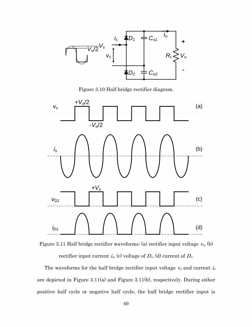
69
is
RL
Io
Vo/2Vs
vs
Co1 +
Vo
-
D1
D2 Co2
Figure 3.10 Half bridge rectifier diagram.
vs
+Vo/2
-Vo/2
(a)
is
vD1
+Vo
(c)
(b)
(d)iD1
Figure 3.11 Half bridge rectifier waveforms: (a) rectifier input voltage vs, (b)
rectifier input current is, (c) voltage of D1, (d) current of D1.
The waveforms for the half bridge rectifier input voltage vs and current is
are depicted in Figure 3.11(a) and Figure 3.11(b), respectively. During either
positive half cycle or negative half cycle, the half bridge rectifier input is

70
connected to one of the output capacitor which holds half of the output voltage.
The amplitude of the fundamental for the full bridge rectifier input voltage Vs
and current amplitude Is can be calculated as
2
s oV V (3.16)
s oI I (3.17)
As shown in Figure 3.11(c), during the negative half cycle when D1 is
reversed biased, the voltage stress across D1 is equal to the output DC voltage
Vo. Since D1 only conduct during positive half cycle, their current waveforms
are depicted in Figure 3.9(d), and diode D1 average current can be calculated
as
1
Diode s oI I I (3.18)
When only considering the conduction loss due to the forward voltage drop
VF of the rectifying diodes, the half bridge rectifier efficiency can be
approximately calculated as
2 2
1 1Diode F F
o o o
I V V
V I V (3.19)
3.3.3 Center-tapped full-wave rectifier
The center-tapped full-wave rectifier, also referred as the current doubler,
consists of two diodes connected to the opposite ends of a secondary center-
tapped transformer. The center-tapped point is usually identified as the
ground point or the zero voltage reference point.

71
As shown in Figure 3.12, if an AC voltage signal is applied to the primary
winding of the transformer, the two secondary voltages will become positive
and negative alternately. For the positive half cycle of the AC voltage, diode D1
will be forward biased and diode D2 will be reverse biased. Therefore, diode D1
will conduct and D2 will not conduct during the positive half cycle, and the
current flows through the load. During the negative half cycle, diode D1 anode
will be negative and D2 anode will be positive with the center-tapped point
being the ground. Thus, diode D2 will be forward biased and D1 will be reverse
biased. Diode D2 will conduct and D1 will not conduct during the negative half
cycle. The direction of current flowing through the load is the same as before.
RL
D1
D2
Covs1
vs2
is
+
Vo
-
io
VoVs1, Vs2
Figure 3.12 Center-tapped full-wave rectifier diagram.

72
vs1, vs2
+Vo
-Vo
(a)
is
vD1
+Vo
(c)
(b)
(d)iD1
Figure 3.13 Center-tapped full-wave rectifier waveforms: (a) rectifier input
voltage vs1 and vs2, (b) rectified current is, (c) voltage of D1, (d) current of D1.
The waveforms for the center-tapped full-wave rectifier input voltage vs1, vs2
and current is are depicted in Figure 3.13(a) and Figure 3.13(b), respectively.
The amplitude of the fundamental for the current doubler input voltage Vs and
current amplitude Is can be calculated as
4
s oV V (3.20)
2s oI I (3.21)
As shown in Figure 3.13(c), during the negative half cycle when D1 is
reversed biased, the voltage stress across diode D1 is equal to the output DC
voltage Vo. Since D1 only conduct during positive half cycle, its current

73
waveforms are depicted in Figure 3.13(d), and diode D1 average current can be
calculated as
1 1
2Diode s oI I I (3.22)
When only considering the conduction loss due to the forward voltage drop
VF of the rectifying diodes, the half bridge rectifier efficiency can be
approximately calculated as
2
1 1Diode F F
o o o
I V V
V I V (3.23)
3.3.4 Output rectifier comparison
This section provided a brief overview of three commonly output AC-DC
rectifiers that can be possibly used in the IPT systems.
The full bridge rectifier has the highest component count, hence increase
the overall cost of the system. The voltage stress of each diode is equal to the
output voltage Vo, and the current stress is equal to half of the output current
Io. The full bridge rectifier input voltage vs swings between +Vo and -Vo, hence
the rectifier input current amplitude Is is equal to times the output current
Io. Owing to the high device count, the full bridge rectifier loss percentage can
be roughly estimated as 2VF/Vo. Utilizing synchronous rectification will help
increase the system efficiency, but also brings more control complexity to the
circuit.
The voltage doubler contains two diodes, hence the cost is moderate. Similar
to that in the full bridge rectifier, the voltage stress of each diode in the voltage

74
doubler is equal to the output voltage Vo. However, the current stress here is
equal to the load output current Io, which is twice as that in the full bridge
rectifier. Therefore, the voltage doubler loss percentage is the same as that in
the full bridge rectifier, or even slightly lower since the diode forward voltage
VF tends to increase when the diode current stress is higher. Furthermore, the
voltage doubler input voltage vs swings between +Vo/2 and -Vo/2, hence the
rectifier input current amplitude Is times the output current Io,
which is twice as that in the full bridge rectifier. Therefore, the secondary
winding conduction loss is higher compared to that for a full bridge rectifier
with same output requirement. This feature renders the voltage doubler
feasible for medium power (<500 W) applications, especially when the required
DC output voltage is much higher than the given DC input voltage.
The current doubler also consists of two rectifying diodes, hence the cost is
modest. Like the previous introduced rectifiers, the current doubler diode
voltage stress is equal to the output voltage. Moreover, the current stress is
equal to that in the full bridge rectifier, which is half of that in the half bridge
rectifier. Therefore, the full bridge rectifier loss percentage is half of that in
the previous two rectifiers, resulting the highest efficiency among the three
rectification circuits. Self-driven synchronous rectification can be easily
implemented in the current doubler owing to the existence of the center-tapped
point. The secondary winding voltage swings between +Vo and -Vo, hence the
rectifier input current is same as that in the full bridge rectifier. Owing to the

75
center-tapped secondary winding structure, the winding loss will be twice as
that for the full bridge rectifier. Moreover, in IPT systems, it is difficult to
maintain the symmetry of two secondary windings especially when gap
variation or misalignment occurs, which leads to imbalance voltage and
current for positive and negative cycle.
Table 3-2 lists all the output rectifiers that have been discussed in this
section and provides a comparison between them in terms of diode count,
device voltage and current stress, rectifier input voltage and current, and loss
percentage.
Table 3-2 Summary and comparison between the output rectifiers
Rectifier Full bridge Half bridge Center-Tapped
Diode count 4 2 2
VDiode_max Vo Vo Vo
IDiode_avg 1/2·IO IO 1/2·IO
vs_max Vo 1/2·Vo Vo
is_rms π 2√2⁄ ·IO π √2⁄ ·IO π 2√2⁄ ·IO
Loss % 2VF/Vo 2VF/Vo VF/Vo
3.4 Loosely coupled transformer model
As mentioned in previous chapters, the LCT is the especial element in an
IPT system, since power transfer of the system is achieved via magnetic
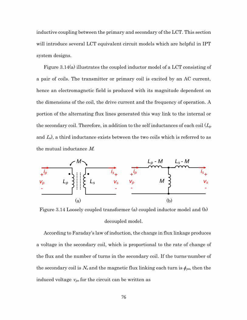
76
inductive coupling between the primary and secondary of the LCT. This section
will introduce several LCT equivalent circuit models which are helpful in IPT
system designs.
Figure 3.14(a) illustrates the coupled inductor model of a LCT consisting of
a pair of coils. The transmitter or primary coil is excited by an AC current,
hence an electromagnetic field is produced with its magnitude dependent on
the dimensions of the coil, the drive current and the frequency of operation. A
portion of the alternating flux lines generated this way link to the internal or
the secondary coil. Therefore, in addition to the self inductances of each coil (Lp
and Ls), a third inductance exists between the two coils which is referred to as
the mutual inductance M.
Lp Ls
M
isip+
vp
-
+
vs
-
Lp - M Ls - M
M
isip+
vp
-
+
vs
-
(a) (b)
Figure 3.14 Loosely coupled transformer (a) coupled inductor model and (b)
decoupled model.
According to Faraday’s law of induction, the change in flux linkage produces
a voltage in the secondary coil, which is proportional to the rate of change of
the flux and the number of turns in the secondary coil. If the turns-number of
the secondary coil is Ns and the magnetic flux linking each turn is ɸps, then the
induced voltage vps for the circuit can be written as

77
( ) ( )
( )ps ps
ps s
d t d tv t N
dt dt
(3.24)
The current in the second coil induces a magnetic field which opposes the
change in mutual flux from the primary coil. This means that the total flux
linkage for the second coil λs is defined as a combination of the mutual flux
linkage λps and the self flux linkage λss shown below:
( ) ( ) ( )s ps sst t t (3.25)
However just like the current in the primary coil induces a magnetic flux
which partially passes through the second, the induced current induces a
magnetic flux which partially passes the primary coil. This means that the
total flux linkage for the primary coil is also a combination of the self flux
linkage λpp and mutual flux linkage λsp as calculated below:
( ) ( ) ( )p pp spt t t (3.26)
Based on the definition of inductance, (3.25) and (3.26) can be rewritten in
terms of inductances as
( ) ( ) ( )p p p sp st L i t M i t (3.27)
( ) ( ) ( )s ps p s st M i t L i t (3.28)
It can be proved that both mutual inductances Mps and Msp are equal by
calculating the amount of energy stored in the circuit due to a change in either
currents flowing into the coils. Hence,
ps spM M M (3.29)

78
By differentiating both sides and then applying Faraday’s law of induction
on the left side, (3.27) and (3.28) can be rewritten to show the relationship
between the input voltage and current, and the output voltage and current as
below
( ) ( )
( )p s
p p
di t di tv t L M
dt dt (3.30)
( ) ( )
( )p s
s s
di t di tv t M L
dt dt (3.31)
The mutual inductance M specifies the strength of coupling between two
coils by comparing the mutual inductance to their self inductances. A coupling
coefficient kc can be defined as the ratio between the mutual inductance and
the self inductances of the coil shown below:
c
p s
Mk
L L (3.32)
The coupling coefficient is zero if there is no coupling between the two coils,
i.e. the magnetic flux produced by either coil does not enter the other. The
coupling coefficient is unity when there is a perfect coupling between the two
coils, i.e. all of the magnetic flux produced by either coil enters the other. For
kc < 0.5, the two coils are considered as loosely coupled, and for kc > 0.5, the
two coils are considered as tightly coupled. The coupling coefficient is a
function of the dimension of the coils and their position with respect to each
other. IPT applications can be considered as a loosely coupled system due to
the large gap between the primary and secondary coils.

79
Figure 3.14(b) is the decoupled equivalent circuit, also referred to as the T-
model of the transformer, which is more feasible for the system model analysis
and calculation.
Figure 3.15 depicts a lumped leakage inductance equivalent circuit for the
LCT. This model consists of the lumped leakage inductance Lr in the primary
side, magnetizing inductance Lm seen from primary coil, and an ideal
transformer with equivalent turns ratio Ne : 1.
Ne : 1Lr
Lm
ip im+
vp
-
+
vs
-
is
Figure 3.15 Lumped leakage inductance model for LCT.
Similarly to the analysis for the coupled inductor model, the relationship
between the input voltage and current, and the output voltage and current can
be derived as below
( ) ( )
( )p m
p r m
di t di tv t L L
dt dt (3.33)
( )
( ) m ms
e
L di tv t
N dt (3.34)
From the characteristics of the ideal transformer,
1
( ) ( ) ( )m p s
e
i t i t i tN
(3.35)

80
By substituting (3.35) into (3.33) and (3.34), the equations can be rewritten
as
( ) ( )
( )p sm
p r m
e
di t di tLv t L L
dt N dt (3.36)
2
( ) ( )( )
p sm ms
e e
di t di tL Lv t
N dt N dt (3.37)
When comparing the inductances portion among (3.30), (3.31), (3.36) and
(3.37), the following equations can be derived.
2
21p s
r c p
s
L L ML k L
L
(3.38)
2
2
m c p
s
ML k L
L (3.39)
p
e c
s s
LMN k
L L (3.40)
This lumped leakage inductance model is suitable for resonant circuits with
only primary side compensation, such as class-E resonant inverter or LLC
resonant converter.
If the LCT is directly applied to an IPT without any compensation network,
when considering its primary and secondary side winding parasitic resistance
rp and rs, its equivalent circuit model is depicted in Figure 3.16.

81
Lp - M Ls - M
M RL
ip is
rp
ip-is
rs
+
vp
-
+
vs
-
Figure 3.16 LCT without compensation in and IPT system.
The phasor representation of the relationship between the primary voltage
Vp and current Ip, and the secondary voltage Vs and current Is when
considering winding parasitic resistances is shown as
p p p p
s s s s
V r j L j M I
V j M r j L I
(3.41)
The total impedance connected to the power source can be derived as shown
below:
2 2
T p p L s s
p p
L s s
Z r j L M j M R r j L M
Mr j L
R r j L
(3.42)
Based on Kirchhoff’s voltage law (KVL), the relationship between primary coil
current ip and secondary coil current is is determined by
p s L s s s
s
p L s s
j M I I R r j L M I
I j M
I R r j L
(3.43)
Combine (3.42) and (3.43), the efficiency of the LCT can be derived as
2
2 2
2 2 2
Re1
s L L
p L ssp Tp L s
I R R
r R rLI Zr R r
M M
(3.44)
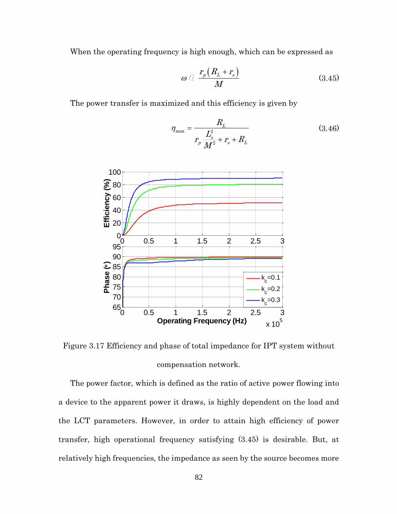
82
When the operating frequency is high enough, which can be expressed as
p L sr R r
M
(3.45)
The power transfer is maximized and this efficiency is given by
max 2
2
L
sp s L
R
Lr r R
M
(3.46)
Figure 3.17 Efficiency and phase of total impedance for IPT system without
compensation network.
The power factor, which is defined as the ratio of active power flowing into
a device to the apparent power it draws, is highly dependent on the load and
the LCT parameters. However, in order to attain high efficiency of power
transfer, high operational frequency satisfying (3.45) is desirable. But, at
relatively high frequencies, the impedance as seen by the source becomes more
0 0.5 1 1.5 2 2.5 3
x 105
0
20
40
60
80
100
Eff
icie
ncy (
%)
0 0.5 1 1.5 2 2.5 3
x 105
65
70
75
80
85
90
95
Operating Frequency (Hz)
Ph
ase ()
kc=0.1
kc=0.2
kc=0.3

83
and more inductive in nature as illustrated in Figure 3.17. As a result, the
power factor becomes very small and starts approaching zero as the frequency
increases. This means that the high frequency source side inverter should have
a large VA rating and that the circulating power would also decrease the
efficiency of power transfer. This is one of the major disadvantages of using
basic IPT configuration for power transfer. To overcome this, capacitive
compensation network is recommended and it will be analyzed in the next
section.
3.5 Compensation network
As analyzed in the previous section, a low mutual inductance results in less
voltage across it. The reactive voltage drop across the leakage inductance will
cause a delay between the voltage and the current which leads to a low power
factor and large circulating energy loss.
To keep the power factor as high as possible in a system with inductances
it is necessary to work with resonance. An inductance cause the current to lag
90° compared to the voltage whereas a capacitor leads the current 90°,
expressed by the equations for their impedances.
LZ j L (3.47)
1
CZj C
(3.48)
If these impedances can be matched the phase angles are cancelled out each
other. To determine the value of the compensation component the inductance

84
together with the resonant frequency at which the system works must be
known and is done as shown below:
0
0
1L
C
(3.49)
This gives the value of the capacitance:
2
0
1C
L (3.50)
The resonant angular frequency is defined as
0
1
LC (3.51)
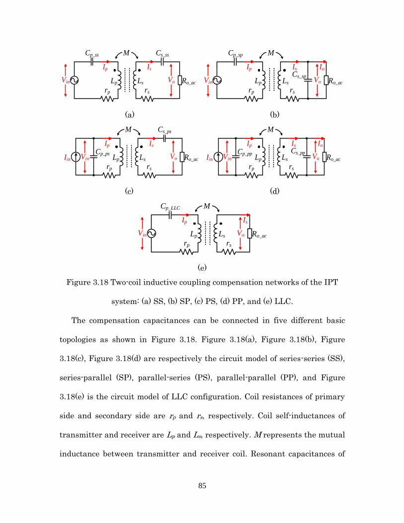
85
Vin
Cp_ss Cs_ss
Ro_acLp Ls
rp rs
Ip Is
M
Vo
Cp_sp
Cs_spRo_acLp Ls
rp rs
Ip
Vin
Is Io
M
Vo
(a) (b)
Iin
Cp_ps
Cs_ps
Lp Ls
Ip
Vin
rp rs
Is
Ro_ac
M
Vo
Cp_pp Cs_pp
Ip
Iin Vin
Is Io
Ro_ac
rp rs
Lp Ls
M
Vo
(c) (d)
Vin
Cp_LLC
Ro_acLp Ls
rp rs
Ip Is
M
Vo
(e)
Figure 3.18 Two-coil inductive coupling compensation networks of the IPT
system: (a) SS, (b) SP, (c) PS, (d) PP, and (e) LLC.
The compensation capacitances can be connected in five different basic
topologies as shown in Figure 3.18. Figure 3.18(a), Figure 3.18(b), Figure
3.18(c), Figure 3.18(d) are respectively the circuit model of series-series (SS),
series-parallel (SP), parallel-series (PS), parallel-parallel (PP), and Figure
3.18(e) is the circuit model of LLC configuration. Coil resistances of primary
side and secondary side are rp and rs, respectively. Coil self-inductances of
transmitter and receiver are Lp and Ls, respectively. M represents the mutual
inductance between transmitter and receiver coil. Resonant capacitances of

86
primary and secondary tank are Cp and Cs respectively. The subscripts _SS, _SP,
_PS, _PP, _LLC indicate different compensation configurations. Ro_ac is the
equivalent load resistance. Currents flowing through the transmitter coil and
receiver coil are Ip and Is, respectively.
Applying KVL to the above five coupling systems, their equivalent circuit
in frequency domain all satisfies the following equation:
0
p pin
s s
Z j M IV
j M Z I
(3.52)
where Zp and Zs are respective impedances of primary and secondary side,
which can be expressed in Table 3-3 for the five different circuits.
Table 3-3 Primary and secondary impedance
Circuit Type Zp Zs
SS 1p p pr j L j C _1s o ac s sr R j L j C
SP 1p p pr j L j C _
1
1s s
s o ac
r j Lj C R
PS p pr j L _1s o ac s sr R j L j C
PP p pr j L _
1
1s s
s o ac
r j Lj C R
LLC 1p p pr j L j C _s o ac sr R j L
From (3.52), it yields
2 2
p
p
p s
Z VI
Z Z M
(3.53)
2 2
inp
p s
j MVI
Z Z M
(3.54)

87
The total impedance ZT connected to the power source for five circuit
systems can be expressed and shown in Table 3-4
Table 3-4 Total impedance of five circuit systems
Circuit Type Total Impedance ZT
SS 2 2
_
11
p p p
s o ac s s
Mr j L j C
r R j L j C
SP
2 2
_
_
1
1
p p po ac
s s
s o ac
Mr j L j C
Rr j L
j C R
PS
2 2
_
1
1
1
p
p p
s o ac s s
j CM
r j Lr R j L j C
PP
2 2
_
_ _
1
1
1
1
p
s o ac
p p
o ac s s s o ac
j CM j C R
r j LR r j L j C R
LLC 2 2
_
1p p p
s o ac s
Mr j L j C
r R j L
Figure 3.18 shows that for a parallel resonant compensated primary (PS,
PP), an equivalent current source is needed. Due to the difficulty of the energy
storage in the form of a simple current source, extra components will be needed
to transfer energy on demand from a voltage source, resulting in extra loss.
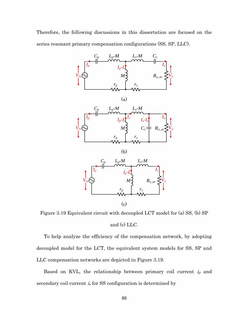
88
Therefore, the following discussions in this dissertation are focused on the
series resonant primary compensation configurations (SS, SP, LLC).
Lp-M Ls-M
M
Cp
Ro_ac
Ip Is
rp
Ip-Is
Cs
rs
VoVin
(a)
Lp-M Ls-M
M
Cp
Ro_ac
Ip IsIp-Is
Cs
IoIs-Io
Vin
rp rs
Vo
(b)
Lp-M Ls-M
M
Cp
Ro_ac
Ip IsIp-Is
rp rs
VoVin
(c)
Figure 3.19 Equivalent circuit with decoupled LCT model for (a) SS, (b) SP
and (c) LLC.
To help analyze the efficiency of the compensation network, by adopting
decoupled model for the LCT, the equivalent system models for SS, SP and
LLC compensation networks are depicted in Figure 3.19.
Based on KVL, the relationship between primary coil current ip and
secondary coil current is for SS configuration is determined by

89
_ _ _ _
_ _ _
1
1
p SS s SS s SS o ac s s s
p SS s SS o ac s s s
I I j M I R r j L M j C
I j M I R r j L j C
(3.55)
The output-to-input voltage gain can be expressed as follows:
_ _ _
_ _ _
_
2 2
_1 1
o SS s SS o ac
in SS p SS T SS
o ac
p p p s o ac s s
V I R
V I Z
j MR
M r j L j C r R j L j C
(3.56)
Combine (3.55) with the total impedance ZT_SS in Table 3-4, the high
frequency inverter output power Pin_SS, the power transferred to the equivalent
load Pout_SS, and the efficiency of the SS compensation network ηT_SS can be
derived as
2
_ _ _Rein SS p SS T SSP I Z (3.57)
2
_ _ _out SS s SS o acP I R (3.58)
_ _
_ 2 2_ _
_ 2 2
1
out SS o ac
T SS
in SS o ac s s s
o ac s p
P R
P R r L CR r r
M
(3.59)
Similarly, the efficiency and voltage gain of the SP and LLC compensation
configuration ηT_SP, ηT_LLC can be calculated as
_
_ 22 2
__2 2 2
_ _ 2 2 2
1
o ac
T SP
s s s o acs s o ac s
o ac s s o ac s p p
R
r L C RL C R rR r C R r r r
M M
(3.60)

90
_ _
_ 2 2
_ _ _
1(1 ) 1
o SP o ac
in SP
s o ac o ac s s s o ac p p
p
V j M R
VM j C R R r j L j C R r j L
j C
(3.61)
_
_ 2 2 2
_
_ 2 2
o ac
T LLC
o ac s s
o ac s p
R
R r LR r r
M
(3.62)
_LLC _
2 2_LLC _
1
o o ac
in p p p s o ac s
v j M R
v M r j L j C r R j L
(3.63)
For any general IPT system, SS compensation network has two major
advantages that make it exceptional useful. One advantage is that the
secondary impedance and therefore the reflected impedance has only a real
component and no reactive component. This means that the secondary coil will
only draw active power when operating at the resonant frequency and there is
no reflected reactance generating additional loss. The other benefit of the SS
compensation network is that the selection of compensation capacitances is
independent of mutual inductance as well as load condition. Therefore, it is
best suited for the condition, where load is drastic, or for the case, where
relative position of secondary is changing with respect to primary, such as in
the case of dynamic charging. The main disadvantage of the SS tuning network
is its relatively high capacitance voltage stress since the capacitors are series
connected with the LCT on both ends. In some high voltage high power
applications, the resonant capacitor voltage can easily reach 10 kV.
91
In the case of SP compensated configuration, the reflected impedance has a
load-independent capacitive reactance at the nominal resonant frequency,
hence fixed frequency operation is possible for different load conditions. The
reflected reactance can be also compensated by the primary inductance
together with the primary series capacitor, but the capacitance is dependent
on the magnetic coupling coefficient. The voltage across the secondary parallel
compensation capacitor is clamped by the output voltage, which is a significant
benefit for the SP tuning configuration.
The LLC compensation network only employs one capacitor series
connected to the LCT in the primary side, without any capacitor in the
secondary side. This feature is ideal for those applications have very limited
room on their receiver ends, such as mobile electronics, biomedical implants or
RFIDs. However, since only primary compensation capacitor is used, the
voltage regulation range of the LLC tuning configuration is relatively narrow
compared to that of SS or SP. Therefore, LLC resonant network is more
suitable for low power constant voltage output applications.
3.6 Summary
This chapter performs some analysis on individual part of an IPT system
including high frequency resonant DC-AC inverter, output AC-DC rectifier,
LCT and its compensation networks.
The full bridge resonant inverter utilizes four active switches which
increase the system cost. However, its moderate voltage and current stress

92
make it suitable for high power applications. Due to the large coil current and
voltage step-down feature of the half bridge resonant inverter, it is more
feasible for medium to low power applications, especially when the required
output voltage is much lower than the given input voltage. The class-E inverter
suffers from its high voltage and current stress on the active switch. However,
only one switch count make it suitable for some low power applications where
system cost is considerably important.
The full-wave bridge rectifier employs four diodes hence its cost is relatively
high. However, its balanced voltage and current stress cause it favorable for
high power applications. Voltage doubler possesses same device voltage as that
in the full bridge rectifier, but twice the current stress on both devices and
secondary winding, which could induce higher conduction loss. Therefore,
voltage doubler is more suitable for medium to low power applications,
especially when the required output voltage is much higher than the given
input voltage. Theoretically the current doubler produces the least conduction
loss among the three output rectifiers. However, it is nontrivial to guarantee
the symmetry of two secondary winding in an IPT system, especially when
relative position between primary and secondary changes.
Three equivalent circuit models for the LCT is analyzed in detail. The
definition and relationship of self inductance, mutual inductance, coupling
coefficient, leakage inductance, magnetizing inductance and effective turns
ratio are derived. The coupled inductor model and the decoupled model are
93
feasible for the system model analysis and calculation. While the lumped
leakage inductance model is suitable for resonant circuits with only primary
side compensation, such as an arrangement called class-E resonant inverter or
LLC resonant converter. If the LCT is directly applied to an IPT without any
compensation network, in order to achieve high power transfer efficiency, the
operating frequency should also be very high, which in turn decreases the
power factor significantly. Therefore, capacitive compensation is required to
overcome this issue.
Five possible tuning network configurations are introduced as SS, SP, PS,
PP and LLC. Since PS and PP configurations are current source driven, extra
components will be needed to transfer energy on demand from a voltage source,
resulting in extra loss. Therefore, three voltage source driven series resonant
primary compensation configurations (SS, SP, LLC) are more of interest in the
IPT systems. Owing to the load and coupling coefficient independency of SS
configuration, it is considered to be best suitable for inductive charging
applications directly connected to the battery. However, its relatively high
voltage stress on the capacitors limit the power transfer capability. SP
configuration is also load-independent but the primary capacitor selection is
dependent on the coupling coefficient. The advantage of SP is the clamped
secondary capacitor voltage. LLC configuration doesn’t have any secondary
compensation capacitor, hence reduce the cost as well as room occupied in the
receiver side. However, its relatively narrow voltage regulation capability

94
makes it more suitable for constant output voltage applications where a post
regulation stage exists before connecting to the battery, e.g. adapters.

95
Chapter 4 High Efficiency Inductive Power Transfer System for
Electric Vehicle Battery Charging Application
4.1 Introduction
Nowadays, the most commonly used method to charge these vehicle
batteries is plug-in charging, which connects the EVs to the electric grid to
charge their batteries via a cable. The charging power level varies from level 1
to level 2 with power up to 19.8 kW [186]-[187]. Major drawbacks of plug-in
charging are bulky and messy cable wires and the exposure to electric plugs
that may cause safety issues. In an effort to overcome these drawbacks,
inductive charging has been investigated in recent years [188]-[189]. A
inductive EV charging system such as the one depicted in Figure 4.1
demonstrates many advantages including convenience of being cordless
making it unnecessary to plug and unplug the bulky cable, insusceptible to
weather impact since the primary side can be embedded underground, and
inherently safe during high power charging.
Receiver
Transmitter
Ground
InverterPFC
Rectifier
Cp
Cs
Motor
Drive
Battery
Motor
Grid
Figure 4.1 Structure of an inductive charging system for EV.

96
As discussed in chapter 2, the early stage of inductive charging was limited
to a few hundred hertz switching frequency due to the limitations of the
semiconductor switching capability, which made it expensive and poor
efficiency [188]. As the semiconductor switch progressed, these limitations
were curtailed, with newer systems able to operate at higher switching
frequencies and increased efficiency. Today, most contactless EV battery
charging systems use insulated-gate-bipolar-junction-transistors (IGBTs) as
the switching devices, which are typically limited to a switching frequency
below 100 kHz due to excessive switching losses, and thus the total system
efficiency including the LCT and all the converter circuits is below 90% [189]-
[193]. Such a relatively low efficiency becomes an obstacle for the practical
implementation of contactless charging for electric vehicles since traditional
plug-in type on-board chargers can achieve a system efficiency greater than
97% [194]-[195].
With a large air gap, the coupling coefficient of the inductive charging
transformer coils is usually from 0.1 to 0.5, which means the leakage
inductances are dominant, and the magnetizing inductance is quite small that
tends to draw a large magnetizing current and results in high circulating
energy loss. As mentioned in chapter 3, capacitive compensation networks are
necessary to solve this issue. Among them, the SS configuration has a desired
characteristic that makes the primary compensation capacitance independent
of load and the magnetic coupling coefficient. However, most of existing designs

97
adopted fixed switching frequency operation to simplify the control. As a result,
the system efficiency suffers when the load or coupling condition changes
during the charging period.
In this chapter, an inductive charging system using SS compensation
configuration with variable switching frequency for EV battery charging
application is proposed. The compensation network efficiency has been
thoroughly analyzed and a methodology to improve the efficiency is proposed.
The input impedance of SS circuit with well-tuned transformer parameters
and compensation capacitances can always be inductive, ensuring ZVS for all
the primary switches in the full range of an EV battery charging. This allows
power MOSFETs with high speed switching and low on-drop resistance (Rds_on)
to be used. The design of a LCT is simulated and verified by FEA software. A
4-kW hardware prototype has been built and tested accordingly. Experiment
results with 4-cm and 8-cm air gaps achieved a peak efficiency of 98% and
96.6%, respectively. The prototype inductive charging system was installed
and tested in an EV to demonstrate the entire charging cycle that includes
constant current (CC) and constant voltage (CV) charging periods using
wireless signal communication. Charging profile under CC and CV charging
modes and their transition are shown to verify the design validity of both
wireless power and signal transmissions.
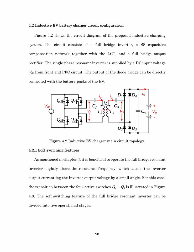
98
4.2 Inductive EV battery charger circuit configuration
Figure 4.2 shows the circuit diagram of the proposed inductive charging
system. The circuit consists of a full bridge inverter, a SS capacitive
compensation network together with the LCT, and a full bridge output
rectifier. The single-phase resonant inverter is supplied by a DC input voltage
Vdc from front-end PFC circuit. The output of the diode bridge can be directly
connected with the battery packs of the EV.
Co
Vdc
Q1
Q2 Q3
Q4
Cp CsM
+
Vo
-
Io
Lp Ls
D1 D4
D2 D3
ip is
vp vs
Figure 4.2 Inductive EV charger main circuit topology.
4.2.1 Soft-switching features
As mentioned in chapter 3, it is beneficial to operate the full bridge resonant
inverter slightly above the resonance frequency, which causes the inverter
output current lag the inverter output voltage by a small angle. For this case,
the transition between the four active switches Q1 ~ Q4 is illustrated in Figure
4.3. The soft-switching feature of the full bridge resonant inverter can be
divided into five operational stages.

99
G1, G3
G2, G4
vp
+Vdc
-Vdc
(a)
(b)
(c)
Tdead
(d)ip
tt0 t1 t2 t3
Q2
Q4Ceq
DQ1
DQ3
Q1,
Q3
Q1,
Q3
Figure 4.3 Switching diagrams of the resonant inverter: (a) Q1 and Q3 gate
signals, (b) Q2 and Q4 gate signals, (c) inverter output voltage vp, (d) inverter
output current ip.
t ≤ t0
Before the time instant t0, Q2 and Q4 are ON while Q1 and Q3 are OFF, the
inverter output current ip flows through the active switches hence its polarity
is negative.
t0 ≤ t ≤ t1
The transition starts at t0 when Q2 and Q4 turn OFF, starting the dead-
time interval. Ceq represents the total parasitic capacitance seen between the
switches drain and source terminals. During this period, the resonant inverter
current discharges the parasitic capacitors of Q1 and Q3, at the same time

100
charges the parasitic capacitors of Q2 and Q4. Therefore the resonant inverter
output voltage vp increase gradually from -Vdc to +Vdc.
t1 ≤ t ≤ t2
At time instant t1, the parasitic capacitors across Q2 and Q4 are fully
charged, while the parasitic capacitors of Q1 and Q3 are fully discharged.
During this period, the body diodes of Q1 and Q3 start conducting output
current.
t2 ≤ t ≤ t3
At time instant t2, the gate signals for switches Q1 and Q3 become high and
the dead-time interval is ended. Due to the low Rds_on of the MOSFETs, the
output current naturally commutates from the body diodes to the device
channels of Q1 and Q3, and the soft-switching characteristic is achieved.
t ≥ t3
At time instant t2, the resonant inverter output current become positive,
and Q1 and Q3 continue conducting the current until their turn OFF signals
arrive.
As one may see from Figure 4.3, the dead time should be long enough to
ensure that the energy exchange between the parasitic capacitors has been
completed. On the other hand, if the inverter output current is not able to
discharge an equivalent capacitor in time, it will be abruptly discharged
through the active switch at time instant t1. Since the dissipated energy can
be substantial, switch thermal failure may occur.
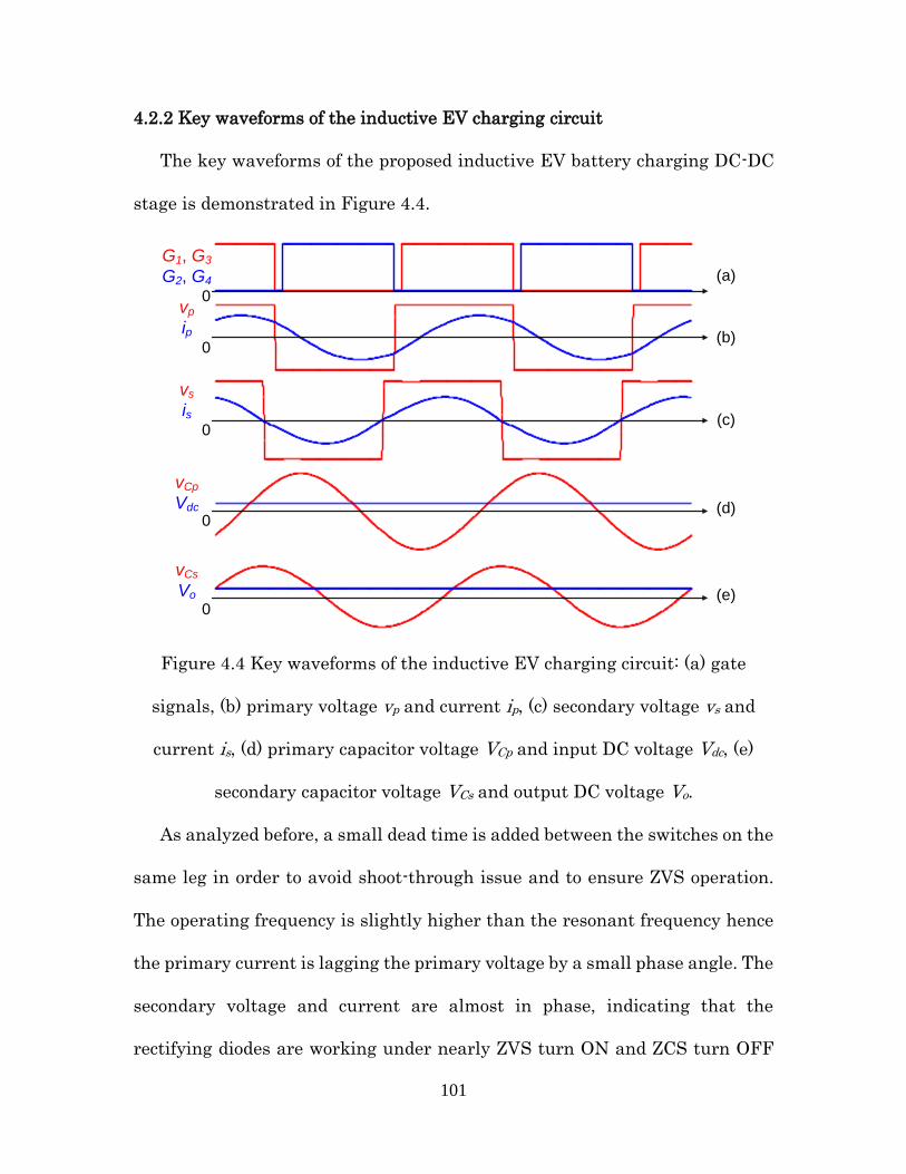
101
4.2.2 Key waveforms of the inductive EV charging circuit
The key waveforms of the proposed inductive EV battery charging DC-DC
stage is demonstrated in Figure 4.4.
G1, G3
G2, G4
vp
ip
vs
is
vCp
Vdc
vCs
Vo
(a)
(b)
(c)
(d)
(e)
0
0
0
0
0
Figure 4.4 Key waveforms of the inductive EV charging circuit: (a) gate
signals, (b) primary voltage vp and current ip, (c) secondary voltage vs and
current is, (d) primary capacitor voltage VCp and input DC voltage Vdc, (e)
secondary capacitor voltage VCs and output DC voltage Vo.
As analyzed before, a small dead time is added between the switches on the
same leg in order to avoid shoot-through issue and to ensure ZVS operation.
The operating frequency is slightly higher than the resonant frequency hence
the primary current is lagging the primary voltage by a small phase angle. The
secondary voltage and current are almost in phase, indicating that the
rectifying diodes are working under nearly ZVS turn ON and ZCS turn OFF

102
condition, which decreases the switching loss of the full bridge rectifier.
However, the major disadvantage of SS compensation configuration is revealed
from Figure 4.4(d) and Figure 4.4(e), which show extensive voltage stresses on
both primary and secondary compensation capacitors.
4.3 Design of the compensation network parameters
This section analyzes the possible compensation network parameters that
could affect the system efficiency. A comprehensive design methodology for the
tuning network to improve the system efficiency is proposed and corresponding
design example is provided.
4.3.1 Effect of parameters on compensation network efficiency
In order to study the parameter variation effect on the SS compensation
network efficiency, every parameter in (3.59) is varied over the entire range
while keeping the other parameters constant. The predetermined range of
these parameters is listed in Table 4-1.
Table 4-1 Parameters value of compensation network
Parameters Symbol Value
Equivalent load resistance (Ω) RL 40 ~ 800
Primary self inductance (µH) Lp 120
Secondary self inductance (µH) Ls 120
Mutual inductance (µH) M 15 ~ 60
Primary capacitance (nF) Cp 10 ~ 500
Secondary capacitance (nF) Cs 10 ~ 500
Operating frequency (kHz) fs 10 ~ 300
Primary winding resistance (Ω) rp 0.3
Secondary winding resistance (Ω) rs 0.3
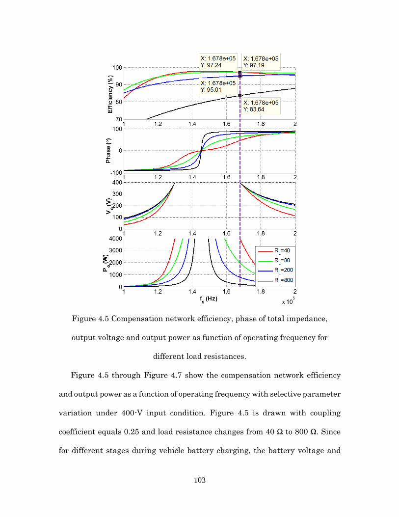
103
Figure 4.5 Compensation network efficiency, phase of total impedance,
output voltage and output power as function of operating frequency for
different load resistances.
Figure 4.5 through Figure 4.7 show the compensation network efficiency
and output power as a function of operating frequency with selective parameter
variation under 400-V input condition. Figure 4.5 is drawn with coupling
coefficient equals 0.25 and load resistance changes from 40 Ω to 800 Ω. Since
for different stages during vehicle battery charging, the battery voltage and

104
charging current are different, which translate to a variable RL. The dashed
line indicates that when the operating frequency is 167.8 kHz, the output
voltage for four cases coincide at 400 V. Therefore, when RL values are 40, 80,
200 and 800 Ω, the corresponding output powers are 4 kW, 2 kW, 800 W and
200 W, respectively. The phase of total impedance curve depicts that under
400-V output condition, when the load resistance increases, the phase angle
increases as well, which means the circulating energy loss is high for light-load
conditions. The efficiency curve also confirms that lower power level results in
lower efficiency with the same output condition.
Figure 4.6 Efficiency, phase of total impedance and output power as function
of operating frequency for different compensation capacitances.

105
Figure 4.7 Efficiency, phase of total impedance and output power as function
of operating frequency for different coupling coefficient.
Figure 4.6 is plotted under the condition of RL = 40 Ω and kc = 0.25. It shows
that when compensation capacitances increase, to maintain the same output
power at 4 kW, the corresponding operating frequency to achieve peak
efficiency will decrease, and the peak efficiency will also decrease. Figure 4.7
is drawn with RL set to 40 Ω. It reveals that to achieve same output power at
4kW, the corresponding peak efficiency operating frequency will increase as
the coupling coefficient increases, and the peak efficiency will increase as well.
There are two inductive regions for the kc = 0.5 case with low output equivalent
resistance, while only one inductive region for the kc = 0.125 and kc = 0.25
cases. The inductive region jump in Figure 4.7 is also referred as “Bifurcation”

106
phenomenon [196]-[197]. From the comparison among three coupling
coefficient cases in Figure 4.7, bifurcation phenomenon tends to occur under
high coupling coefficient conditions.
4.3.2 Design methodology for SS Tuning Network Parameters
Before designing SS compensation network with LCT, some design targets
should be predefined, for example, the battery charging profile, geometry
requirements, and frequency range limits. The battery charging profile can
help determine the equivalent load resistance and power rating of the system.
Geometry requirements include the total space available on the vehicle for the
secondary stage and gap distance variation between primary coil and
secondary coil. According to the efficiency analysis above, peak efficiency
occurs when fs is equal to f0, and higher f0 would result in higher peak efficiency.
However, it is impractical to select f0 as large as possible, since it will also
increase the current and voltage stress on the coils and capacitors. The
operating frequency is also limited by the switching capability of
semiconductor devices.
The first step of the design procedure is to select initial self inductances of
primary and secondary coil based on the geometry limitation. Since high
coupling and heavy load conditions bring more possibility of bifurcation, the
design should consider highest coupling and heavy load conditions as the worst
case. The tuning network design methodology flow chart is shown in Figure
4.8.
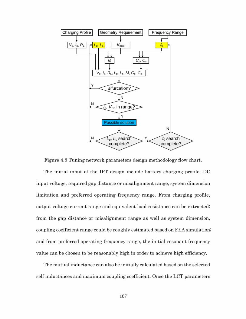
107
Charging Profile Geometry Requirement Frequency Range
Vo, Io, RL Kmax f0Lp, Ls
M Cp, Cs
Vo, Io, RL, Lp, Ls, M, Cp, Cs
Bifurcation?Y
N
Ip, VCp in range?N
Y
Possible solution
Lp, Ls search
complete?
YN f0 search
complete?
N
Figure 4.8 Tuning network parameters design methodology flow chart.
The initial input of the IPT design include battery charging profile, DC
input voltage, required gap distance or misalignment range, system dimension
limitation and preferred operating frequency range. From charging profile,
output voltage current range and equivalent load resistance can be extracted;
from the gap distance or misalignment range as well as system dimension,
coupling coefficient range could be roughly estimated based on FEA simulation;
and from preferred operating frequency range, the initial resonant frequency
value can be chosen to be reasonably high in order to achieve high efficiency.
The mutual inductance can also be initially calculated based on the selected
self inductances and maximum coupling coefficient. Once the LCT parameters

108
and resonant frequency are selected, in order to achieve maximum power
transfer, resonant capacitances Cp and Cs are calculated as
0
1 1
p p s sL C L C (4.1)
Primary and secondary quality factors are derived as follows:
_
2
0
p o ac
p
L RQ
M (4.2)
0
_
ss
o ac
LQ
R
(4.3)
Once all the parameters for the compensation network are selected, in
accordance to the battery charging profile, the real-time operating frequency
for the whole charging procedure can be projected. Under any charging states,
in another word for any output voltage and current requirement from the
charging profile, there should be one and only one steady state operating
frequency within ZVS region to fulfill ZVS operation and avoid bifurcation. If
there were two ZVS regions, the single steady state frequency should be located
in second ZVS region to avoid operating point moving over ZCS region. If
parameters set could fulfill these requirements for the whole charging profile,
then the set is one possible solution. At the same time, the current and voltage
stress on the coil and capacitor can also be calculated based on the following
equations:
4 dc
p
T
Vi
Z (4.4)

109
4 1dc
Cp
T p
Vv
Z j C (4.5)
If there is not a valid solution for the operating frequency for the whole
charging period without bifurcation phenomenon, or the current and voltage
stress exceed the predetermined value, another iteration should be performed,
until all these requirements are fulfilled. It is possible to find more than one
parameter set complying with all the requirements, and in order to identify
the optimal design solution the weighted average efficiency during the whole
charging procedure and system cost can be employed as the optimization
targets.
4.3.3 Design example
Figure 4.9 illustrates the detailed geometrical dimensions of a LCT with 8-
cm air gap, as well as its FEA simulation model. In general, a larger diameter
should yield a better coupling coefficient but with the penalty of winding cost
and limitation of the mounting space. In this case, the selection of 23.5-cm coil
diameter is based on the mounting space available in a test vehicle. Both
primary and secondary windings are manufactured with 28 turns AWG12
equivalent Litz wire. Instead of one solid ferrite plate, 12 small ferrite I-shape
bars are utilized for each side of the transformer to reduce weight and cost, as
well as help shaping the magnetic field and provide some shielding.
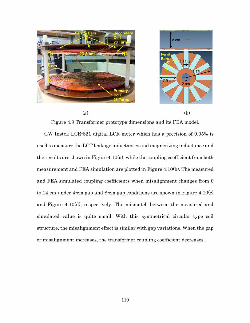
110
(a) (b)
Figure 4.9 Transformer prototype dimensions and its FEA model.
GW Instek LCR-821 digital LCR meter which has a precision of 0.05% is
used to measure the LCT leakage inductances and magnetizing inductance and
the results are shown in Figure 4.10(a), while the coupling coefficient from both
measurement and FEA simulation are plotted in Figure 4.10(b). The measured
and FEA simulated coupling coefficients when misalignment changes from 0
to 14 cm under 4-cm gap and 8-cm gap conditions are shown in Figure 4.10(c)
and Figure 4.10(d), respectively. The mismatch between the measured and
simulated value is quite small. With this symmetrical circular type coil
structure, the misalignment effect is similar with gap variations. When the gap
or misalignment increases, the transformer coupling coefficient decreases.
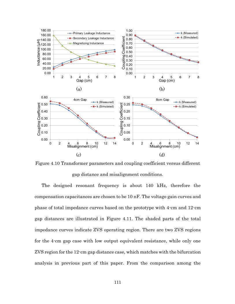
111
(a) (b)
(c) (d)
Figure 4.10 Transformer parameters and coupling coefficient versus different
gap distance and misalignment conditions.
The designed resonant frequency is about 140 kHz, therefore the
compensation capacitances are chosen to be 10 nF. The voltage gain curves and
phase of total impedance curves based on the prototype with 4-cm and 12-cm
gap distances are illustrated in Figure 4.11. The shaded parts of the total
impedance curves indicate ZVS operating region. There are two ZVS regions
for the 4-cm gap case with low output equivalent resistance, while only one
ZVS region for the 12-cm gap distance case, which matches with the bifurcation
analysis in previous part of this paper. From the comparison among the

112
different curves of Figure 4.11, bifurcation phenomenon tends to occur under
heavy load and high coupling coefficient conditions.
(a) (b)
Figure 4.11 Voltage gain and phase curves for (a) 4-cm gap and (b) 12-cm gap.
4.4 Control of the inductive charging system
Figure 4.12 Assumed charging profile of EV battery packs.

113
A typical lithium-ion battery packs charging profile is illustrated in Figure
4.12. At the initial stage of the charging procedure, constant charging current
is required. When the battery voltage reaches a certain level, constant charging
voltage is necessary. In order to fulfill the charging requirement for the whole
charging period that covers both CC and CV modes, a closed-loop control
scheme is adopted as shown in Figure 4.13. The sensed battery voltage and
charging current are compared with their reference values obtained from the
charging profile. The errors are fed to the designed proportional-integral (PI)
controllers with anti-windup function. The mode selection block helps to decide
whether to stay in CC mode or move to CV mode. The frequency limiter helps
prevent the controller from climbing over the peak voltage gain, otherwise, the
system would become a positive feedback system, which would cause the
controller to go to the extreme and saturate. The selected frequency is fed into
the DSP PWM generation module to provide gate signals to the primary switch
gate driver circuitries.
Io
PWM
ModuleGate
Vo
KP
-
+Iref
Ierr
ferr
fupper_limit
+
fsw
-
+Vref
-
Verr
Mode
Selection
KIAnti-
Windup
++
KP
KIAnti-
Windup+
+fsw
fsys_clk Tsw
LimiterDivider
Figure 4.13 Closed-loop control diagram.
The interrupt service routine in the DSP to achieve smooth transition
between CC and CV modes is shown in Figure 4.14. When the controller is
running in CC mode, the current PI controller output should not be saturated.
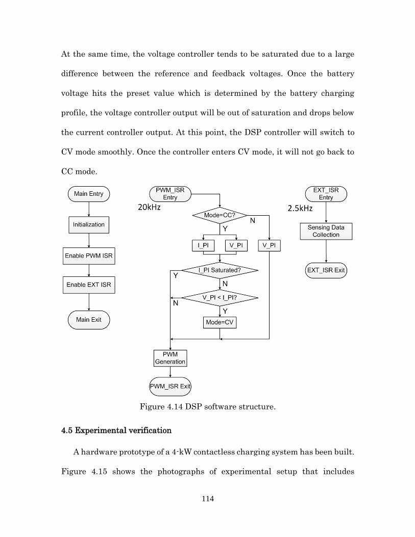
114
At the same time, the voltage controller tends to be saturated due to a large
difference between the reference and feedback voltages. Once the battery
voltage hits the preset value which is determined by the battery charging
profile, the voltage controller output will be out of saturation and drops below
the current controller output. At this point, the DSP controller will switch to
CV mode smoothly. Once the controller enters CV mode, it will not go back to
CC mode.
Figure 4.14 DSP software structure.
4.5 Experimental verification
A hardware prototype of a 4-kW contactless charging system has been built.
Figure 4.15 shows the photographs of experimental setup that includes

115
transformer coils and circuit boards. Four Fluke 289 digital multimeters which
have precisions of 0.025% for DC voltage and 0.15% for DC current are used to
measure the input voltage/current and output voltage/current. The switching
devices used are the 36-mΩ Rds_on SupreMOS FCH76N60N from Fairchild®,
and the rectifier bridge uses fast-recovery diode 80EPF06 from International
Rectifier®. Under 8-cm air gap condition, the primary self inductance is 130
µH, secondary self inductance is 122 µH, and mutual inductance is 31.4 µH,
and coupling coefficient is 0.25. The winding resistance of both rp and rs are
around 0.3 Ω. Both primary and secondary resonant capacitances are 10 nF.
The input DC voltage is 320 V, and output voltage is changing from 250 to 450
V.
Figure 4.15 Experimental setup on the bench.
Figure 4.16(a) and Figure 4.16(b) show the main operation waveforms of
the inductive charging system under full-load condition with 8-cm gap and 4-
cm gap, respectively. The upper two traces indicate that the primary active
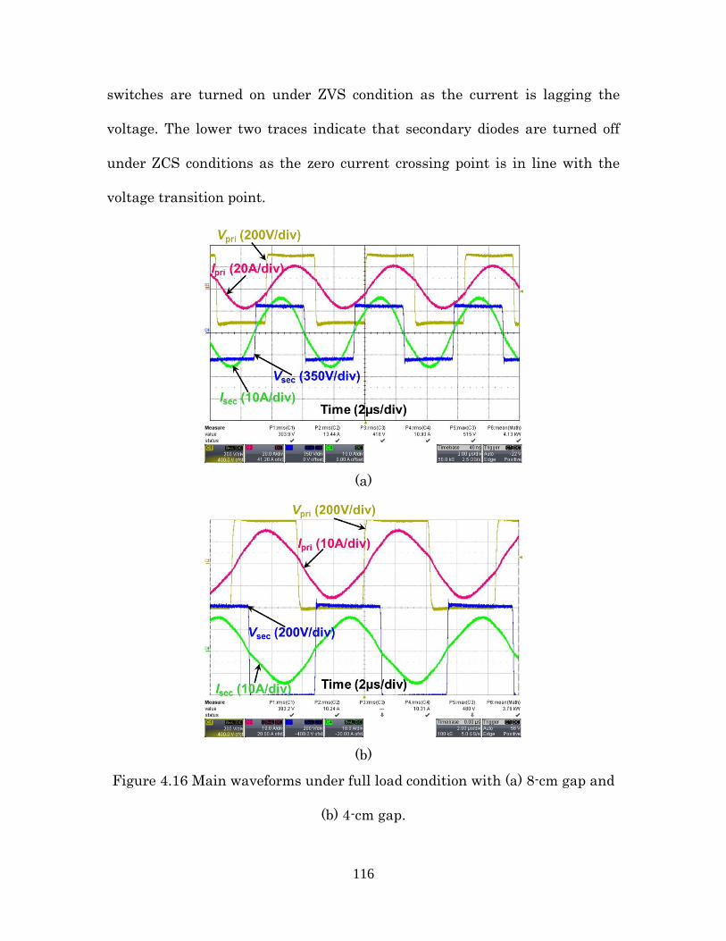
116
switches are turned on under ZVS condition as the current is lagging the
voltage. The lower two traces indicate that secondary diodes are turned off
under ZCS conditions as the zero current crossing point is in line with the
voltage transition point.
(a)
(b)
Figure 4.16 Main waveforms under full load condition with (a) 8-cm gap and
(b) 4-cm gap.

117
Figure 4.17 demonstrates the primary and secondary comensation
capacitors voltage stresses. Due to the high voltage stress and the limited
measuring range of the differential voltage probes, the measured voltage is 1/3
of the total voltage stress on the capacitors. Under 4-kW full load condition,
the RMS voltage stresses on the primary and secondary capacitors are 1.6 kV
and 1.0 kV, respectively. Both Figure 4.16 and Figure 4.17 match well with the
analysis shown in section 4.2.2.
Figure 4.17 Capacitor voltage stress for 8-cm gap condition.
Figure 4.18 shows the closed-loop control dynamic response of the
contactless charging system when the current reference has a step increase
from 3 to 6 A and a step decrease from 6 to 3A. The transition time is about 20
ms, which is good enough for battery charging applications. The system
response under a step change of the battery voltage is plotted in Figure 4.19,

118
which indicates a transition time of around 20 ms under step-up and step-down
voltage change.
(a) (b)
Figure 4.18 System response when current reference: (a) step up; (b) step
down.
(a) (b)
Figure 4.19 System response when voltage reference: (a) step up; (b) step
down.
Figure 4.20 depicts a short charging cycle using programmable DC
electronic load (E-load) BK Precision 8526 to simulate a real EV battery
charging profile. When the output voltage reaches the set point of 200 V, the
operating mode switches from constant current to constant voltage seamlessly.
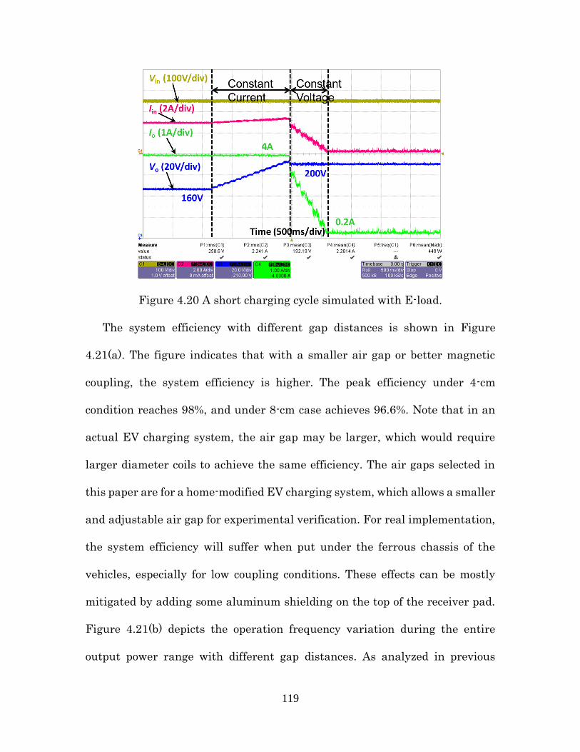
119
Figure 4.20 A short charging cycle simulated with E-load.
The system efficiency with different gap distances is shown in Figure
4.21(a). The figure indicates that with a smaller air gap or better magnetic
coupling, the system efficiency is higher. The peak efficiency under 4-cm
condition reaches 98%, and under 8-cm case achieves 96.6%. Note that in an
actual EV charging system, the air gap may be larger, which would require
larger diameter coils to achieve the same efficiency. The air gaps selected in
this paper are for a home-modified EV charging system, which allows a smaller
and adjustable air gap for experimental verification. For real implementation,
the system efficiency will suffer when put under the ferrous chassis of the
vehicles, especially for low coupling conditions. These effects can be mostly
mitigated by adding some aluminum shielding on the top of the receiver pad.
Figure 4.21(b) depicts the operation frequency variation during the entire
output power range with different gap distances. As analyzed in previous

120
section, it is more likely for the high coupling and heavy load cases to have
bifurcation phenomenon. Therefore, there is an abrupt frequency transition on
the 4-cm efficiency curve. In practical EV charging procedures the ZVS
operation for primary switches should be maintained during the whole
charging period. Frequency jumping from one ZVS region to the other ZVS
region should be avoided, therefore there is a low frequency limit set in the
controller to ensure that the system operates in the high frequency ZVS region.
Figure 4.21(c) shows the efficiency and frequency variation during the entire
output power range for the 4-cm gap condition when the system is operating
in the high frequency ZVS region without any abrupt frequency variation. The
whole output power range can be achieved by changing the frequency from 186
to 191.5 kHz. From the efficiency comparison between Figure 4.21(a) and
Figure 4.21(c), the efficiency under the 4-cm case slightly decreases at heavy
load conditions when operating only in the high frequency region as opposed
to transitioning between the two ZVS regions.
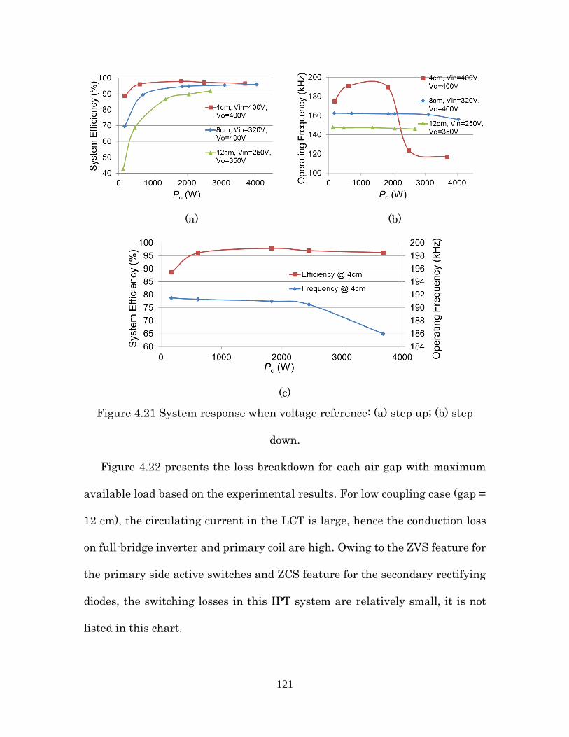
121
(a) (b)
(c)
Figure 4.21 System response when voltage reference: (a) step up; (b) step
down.
Figure 4.22 presents the loss breakdown for each air gap with maximum
available load based on the experimental results. For low coupling case (gap =
12 cm), the circulating current in the LCT is large, hence the conduction loss
on full-bridge inverter and primary coil are high. Owing to the ZVS feature for
the primary side active switches and ZCS feature for the secondary rectifying
diodes, the switching losses in this IPT system are relatively small, it is not
listed in this chart.
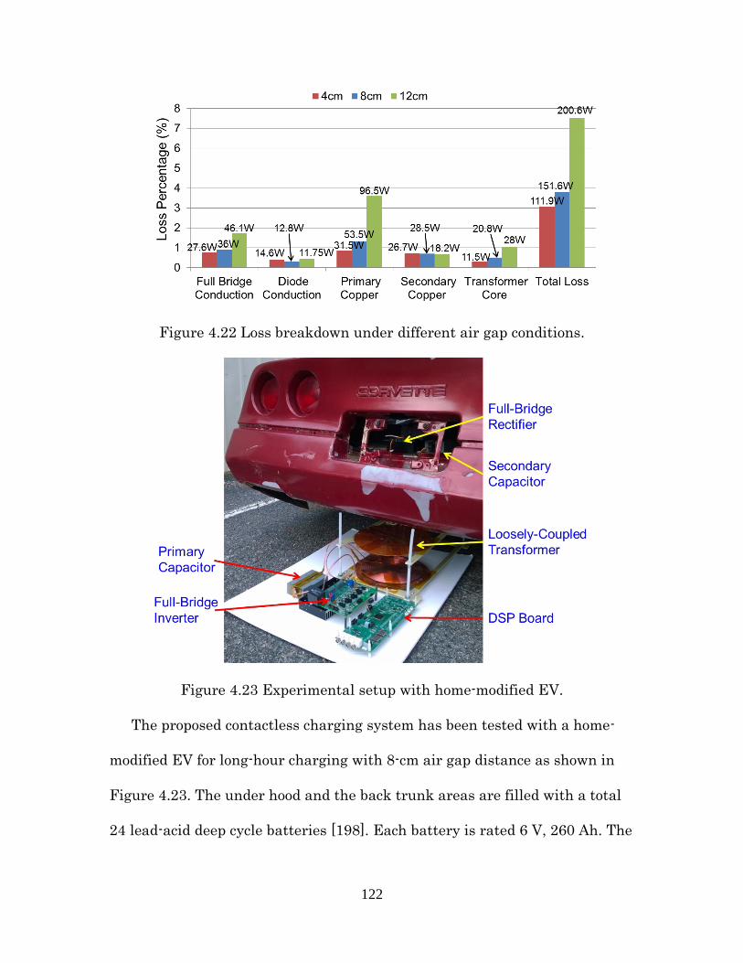
122
Figure 4.22 Loss breakdown under different air gap conditions.
Figure 4.23 Experimental setup with home-modified EV.
The proposed contactless charging system has been tested with a home-
modified EV for long-hour charging with 8-cm air gap distance as shown in
Figure 4.23. The under hood and the back trunk areas are filled with a total
24 lead-acid deep cycle batteries [198]. Each battery is rated 6 V, 260 Ah. The
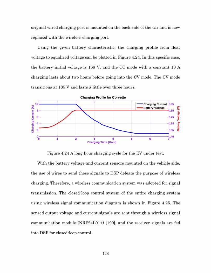
123
original wired charging port is mounted on the back side of the car and is now
replaced with the wireless charging port.
Using the given battery characteristic, the charging profile from float
voltage to equalized voltage can be plotted in Figure 4.24. In this specific case,
the battery initial voltage is 158 V, and the CC mode with a constant 10-A
charging lasts about two hours before going into the CV mode. The CV mode
transitions at 185 V and lasts a little over three hours.
Figure 4.24 A long-hour charging cycle for the EV under test.
With the battery voltage and current sensors mounted on the vehicle side,
the use of wires to send these signals to DSP defeats the purpose of wireless
charging. Therefore, a wireless communication system was adopted for signal
transmission. The closed-loop control system of the entire charging system
using wireless signal communication diagram is shown in Figure 4.25. The
sensed output voltage and current signals are sent through a wireless signal
communication module (NRF24L01+) [199], and the receiver signals are fed
into DSP for closed-loop control.
0 1 2 3 4 5 6 70
2
4
6
8
10
Charging Time (Hour)
Ch
arg
ing
Cu
rren
t (A
)
0 1 2 3 4 5 6 7145
155
165
175
185
195
Batt
ery
Vo
ltag
e (
V)
Charging Profile for Corvette
Charging Current
Battery Voltage

124
Figure 4.25 Closed-loop control with wireless signal communication.
Figure 4.26 shows the experimental charging profiles and efficiency
measurement under both CC and CV charging condition. Figure 4.26(a) shows
the recorded battery voltage and current over the entire charging cycle, which
well agrees with the CC and CV modes shown in Figure 4.24. At the beginning,
the battery voltage is 158 V, and the charger was under CC mode with a fixed
charging current of 9.6 A. The power gradually climbs up as the voltage
increases. At the two-hour mark, the voltage reaches 185 V, the charger
switches to CV mode, and the current or power gradually reduces because the
controller switches from CC to CV mode. Figure 4.26(b) indicates that the
efficiency is above 90% during most of the charging period, and the highest
efficiency is around 96%, which occurs near the peak power of 1.8 kW or the
transition point between CC and CV modes.

125
(a)
(b)
Figure 4.26 Long-hour charging profiles and efficiency measurement using a
home-modified EV.
4.6 Summary
This chapter presents the detailed design procedure of a high-efficiency 4-
kW IPT system using both primary and secondary series connected capacitors
resonant converter with variable switching frequency control for EV battery
charging application. The proposed design procedure describes how to
determine the optimal parameters for the LCT and associated resonant
capacitors. The frequency domain analysis results of the voltage transfer gain
and input impedance allow selection of the switching frequency that minimizes
the circulating energy and switching loss while achieving the desired voltage

126
gain. By achieving ZVS for all of the primary switches, low on-state resistance
MOSFETs can be used to reduce the conduction loss and further improve
system efficiency. Peak system DC-DC efficiencies of 98% and 96.6% are
achieved with 4-cm and 8-cm air gap conditions. Such an efficiency of the
inductive charging system is comparable to the conventional plug-in type or
wired charging systems for EVs.
In addition to testing with E-load, the inductive charger performance was
also successfully verified using batteries in an actual EV environment. A
hardware prototype including both inductive battery charger and wireless
signal communication system was built and tested with a home-modified EV
to demonstrate the actual EV charging condition. Test results with a smooth
transition between CC and CV modes indicated effectiveness of the wireless
communication system for the sensed signals. During a long-hour actual EV
charging period with 8-cm gap setup, 96% peak efficiency was achieved under
the rated charging current but less than half the rated charger voltage
condition.
127
Chapter 5 High Misalignment Tolerance High Efficiency
Inductive Laptop Charger
5.1 Introduction
Despite the IPT system advantages mentioned in the dissertation, there are
still some issues to be addressed otherwise would become obstacles for the
promotion of IPT technology. As an example, gap and horizontal
misalignments between transmitter and receiver would be a critical problem
because the power transfer efficiency greatly depends on the relative positions
of the primary and the secondary coils in the IPT system. Therefore, the power
transfer efficiency is drastically reduced when a gap variation or misalignment
occurs between the inductive coils [22]-[23]. For EV charging applications,
different vehicle ground clearance or misaligned parking of the vehicle will
result in the IPT system operating at a degraded performance of lower power
transfer, reduced efficiency and longer charging time. For biomedical implants
applications, the coils are usually misaligned, because doctor or patient could
not easily identify the implant location or orientation in regular outpatient or
home settings. Therefore, one may have trouble to precisely place the
transmitter coil, which often is embedded in a belt or clothes, held by hands or
supported with a bedside apparatus, in the correct or optimal position outside
the body. Moreover, relative body motions in daily activities or organ/tissue
movement also create uncertainty in estimating the implant position from
outside the body. Therefore, the coupling coefficient is unavoidably impaired.

128
The effects caused by gap variation and horizontal misalignments between
primary and secondary coils should be fully addressed in order to enhance the
efficiency and stability of the IPT system. One possible solution is to employ
additional coils either in the primary side or in the secondary side so that the
effects of gap and misalignment are reduced over a certain range [200]-[203].
One disadvantage of this solution is the required large surface area, since the
available room is always limited, especially for receiver side. At the same time,
the overall system cost and weight will be proportionally increased as the
surface area enlarges. An alternative method that addresses these
shortcomings is to retune the transmitter in order to operate at optimum
switching conditions when the coils are in a misaligned state [204]-[209]. The
main disadvantages of this solution are increased components count and more
complex control strategy for the overall system. Some other researchers
investigated the coil misalignment models as well as mutual inductance and
coupling coefficient expressions based on mathematical derivations [210]-
[214]. The shortcoming for these calculations is the LCTs under investigation
are always air-core coils. However, in practical implementation, in order to
help shape the magnetic flux distribution and limit exposed radiated field to
the ambient environment, some shielding techniques should be employed.
Therefore, the derived mathematical expressions are no longer accurate under
these realistic operation conditions.
129
It is known that coil dimensions and coil shapes substantially affect the
magnitude of the magnetic field which is closely related to the coupling
coefficient of the LCT. In this chapter, design considerations to reduce gap and
misalignment effects for the IPT system are proposed based on the relationship
between the LCT coupling coefficient and several key parameters of the coil
dimensions as well as the aid of FEA simulation. With the designed LCT
geometry parameters, some design considerations based on the effect of the
LCT turns number and operating frequency to the winding and core loss of the
LCT are studied carefully to help improve the system efficiency. A 100-W lab
prototype for laptop inductive charging is implemented to validate the
performance of the proposed design considerations, and the corresponding
experiments are carried out. The experimental results reveal that the proposed
asymmetrical LCT prototype greatly reduces the impact to the coupling
coefficient as well as compensation network efficiency when gap variation or
misalignment occurs.
5.2 Design considerations for gap variation and misalignment tolerance
As analyzed in previous chapters of this dissertation, when the LCT
coupling coefficient increases, in order to achieve same input/output operation
condition, the phase angle of total impedance decreases, which means the
circulating energy loss is low for high coupling conditions. At the same time,
the corresponding operating frequency needs to be increased when the coupling
coefficient of the LCT increases. If the coupling coefficient variation range is

130
large due to gap change or misalignment condition, the required operating
frequency range will be very wide, hence increases the burden of EMI design.
In order to accommodate different gap variation and misalignment conditions,
some design considerations of the LCT are carried out to minimize the coupling
coefficient deviation so as to reduce the operating frequency and system
efficiency variation.
Most LCTs are designed to be symmetrical for transmitter and receiver coil.
This configuration could achieve good coupling coefficient when the coils are
perfectly aligned under desired gap distance condition. However, when gap
variation or misalignment occurs, the coupling coefficient will drop drastically
as the measured results shown in Figure 4.10.
Some simulation models are developed in the three-dimensional FEA
simulation tool to explore the relationships between the LCT coupling
coefficient and several key parameters of the coil dimensions. An example
model is illustrated in Figure 5.1. Figure 5.1(a) shows the placement of the
LCT with ferrite cores on both sides. The windings and cores are separate from
their real position with some gap in order to depict the configuration more
clearly. In real design and FEA simulation, the ferrite plates are put close to
the coils to help shape the magnetic flux distribution and reduce the radiated
interference to the ambient environment. Figure 5.1(b) is the top view of the
investigated model excluding the ferrite cores. The simulation parameters are
listed in Table 5-1. As shown in Figure 5.1(b), the primary outer diameter ODpri

131
and secondary outer diameter ODsec are kept to 200 mm and 100 mm,
respectively.
(a) (b)
Figure 5.1 FEA simulation model. (a) 3-D view. (b) Top view without ferrite
cores.
Table 5-1 FEA simulation parameters
Core Material 3C94
Plate Thickness 1 mm
Primary Core Diameter 200 mm
Secondary Core Diameter 100 mm
Primary Coil Thickness 0.74 mm
Secondary Coil Thickness 2.36 mm
Gap Distance 6~20 mm
Horizontal Misalignment 0~50 mm
5.2.1 Primary coil inner diameter smaller than secondary coil outer diameter
Two scenarios are examined when keeping the primary inner diameter IDpri
to be 50 mm, while changing the secondary coil inner diameter IDsec between
50 mm and 75 mm. The coupling coefficient when the gap distance varies from
6 to 20 mm under the perfect aligned condition is plotted in Figure 5.2(a). The

132
coupling coefficient under the condition of the horizontal misalignment
changes from 0 to 50 mm when the air gap is fixed to 10 mm is illustrated in
Figure 5.2(b). Figure 5.2(a) depicts that when the primary winding inner
diameter is smaller than the secondary winding outer diameter, the coupling
coefficient decreases almost linearly when the gap distance increases, but not
much. On the other hand, Figure 5.2(b) shows that the coupling coefficient
decreases dramatically when the horizontal misalignment becomes larger.
Moreover, with larger inner diameter of the secondary winding, the coupling
coefficient is slightly larger.
(a) (b)
Figure 5.2 Coupling coefficient when primary coil inner diameter is smaller
than secondary coil outer diameter: (a) under gap variation but perfect
aligned condition, (b) under misaligned but fixed gap condition.
5.2.2 Vary inner diameter of primary coil
Three situations are evaluated when keeping the secondary inner diameter
IDsec to be 50 mm, while changing the inner diameter of primary coil IDpri
among 50 mm, 100 mm and 150 mm. The coupling coefficient when gap
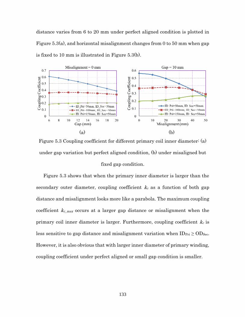
133
distance varies from 6 to 20 mm under perfect aligned condition is plotted in
Figure 5.3(a), and horizontal misalignment changes from 0 to 50 mm when gap
is fixed to 10 mm is illustrated in Figure 5.3(b).
(a) (b)
Figure 5.3 Coupling coefficient for different primary coil inner diameter: (a)
under gap variation but perfect aligned condition, (b) under misaligned but
fixed gap condition.
Figure 5.3 shows that when the primary inner diameter is larger than the
secondary outer diameter, coupling coefficient kc as a function of both gap
distance and misalignment looks more like a parabola. The maximum coupling
coefficient kc_max occurs at a larger gap distance or misalignment when the
primary coil inner diameter is larger. Furthermore, coupling coefficient kc is
less sensitive to gap distance and misalignment variation when IDPri ≥ ODSec.
However, it is also obvious that with larger inner diameter of primary winding,
coupling coefficient under perfect aligned or small gap condition is smaller.

134
Figure 5.4 Magnetic Field Distribution when IDPri = 50 mm, IDSec = 50 mm.
The magnetic field distributions when IDPri = 50 mm and IDSec = 50 mm for
three different misalignment conditions with 10-mm gap are shown in Figure
5.4. The top and bottom gray block represents the cross section of secondary
and primary ferrite core, respectively. The primary and secondary windings
are illustrated by the dark bars. Different color represents different magnetic
intensity as the legend bar shows, from 0 to 5 mT, the color changes from blue
to red. The arrows indicate the flux line direction and the arrow size represents
the magnetic field strength. The coupling coefficient can be revealed by the
magnetic field density B near the secondary coil. The top chart and middle
chart has similar magnetic field intensity around the secondary coil, hence the
coupling coefficients for these two conditions are similar. The bottom chart

135
demonstrates high B near the left edge of secondary coil, but for the rest of the
field B fades out. Therefore, the coupling coefficient for the bottom chart is
smaller compared with the upper two charts, as the coupling coefficient plot
shown in Figure 5.3(b).
5.2.3 Vary inner diameter of primary coil
Two examples are checked when keeping the primary inner diameter IDpri
to be 100 mm which equals the secondary coil outer diameter ODsec, while
changing the secondary coil inner diameter IDsec between 50 mm and 75 mm.
The coupling coefficient when gap distance varies from 6 to 20 mm under
perfect aligned condition is plotted in Figure 5.5(a), and horizontal
misalignment changes from 0 to 50 mm when gap is fixed to 10 mm is
illustrated in Figure 5.5(b).
(a) (b)
Figure 5.5 Coupling coefficient for different secondary coil inner diameter: (a)
under gap variation but perfect aligned condition, (b) under misaligned but
fixed gap condition.

136
Figure 5.5 indicates that with larger secondary inner diameter, averaged
coupling coefficient is larger. Moreover, with smaller secondary inner
diameter, coupling coefficient is less sensitive to misalignment variation.
The magnetic field distribution for fixed 100-mm inner diameter of primary
coil and two different secondary coils with 50-mm and 75-mm inner diameter
under three misalignment conditions are shown in Figure 5.6. In both
scenarios, the primary coil inner diameter equals the secondary coil outer
diameter, and the gap is fixed at 10 mm. For either IDSec case under 0 and 20
mm misalignment conditions, the magnetic intensity around the secondary coil
are similar, hence the coupling coefficients variations are minor. When the
misalignment increases to 50 mm, the induced magnetic field coupled to the
secondary coil drops, therefore the coupling coefficient decreases. From the
comparison between Figure 5.6(a) and Figure 5.6(b), the averaged magnetic
field intensity is higher for the secondary coil with larger inner diameter when
misalignment is 0 and 20 mm, which results in higher coupling coefficient as
shown in Figure 5.5(b). For 50-mm misalignment condition, both cases
demonstrate similar magnetic field distribution, which lead to almost equal
coupling coefficient as depicted in Figure 5.5(b).

137
(a)
(b)
Figure 5.6 Magnetic Field Distribution when (a) IDPri = 100 mm, IDSec = 50
mm and (b) IDPri = 100 mm, IDSec = 75 mm.
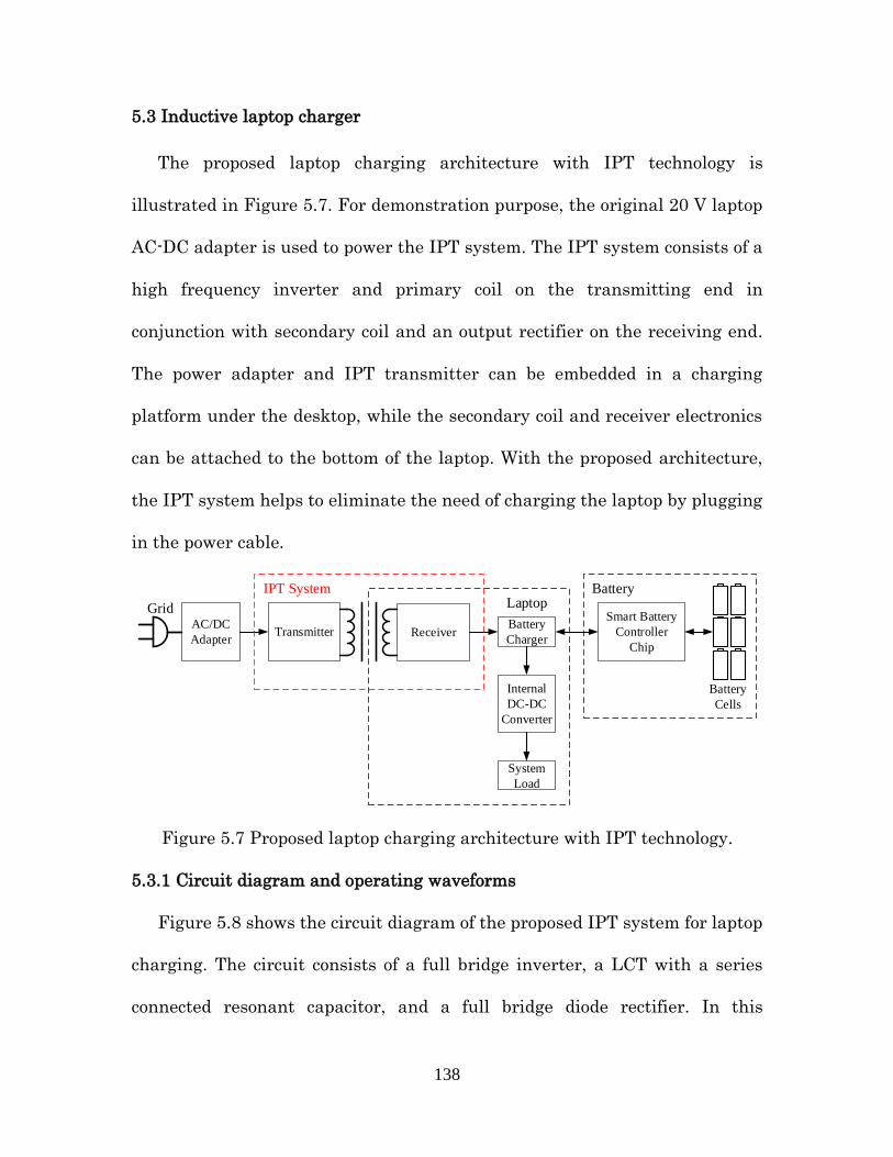
138
5.3 Inductive laptop charger
The proposed laptop charging architecture with IPT technology is
illustrated in Figure 5.7. For demonstration purpose, the original 20 V laptop
AC-DC adapter is used to power the IPT system. The IPT system consists of a
high frequency inverter and primary coil on the transmitting end in
conjunction with secondary coil and an output rectifier on the receiving end.
The power adapter and IPT transmitter can be embedded in a charging
platform under the desktop, while the secondary coil and receiver electronics
can be attached to the bottom of the laptop. With the proposed architecture,
the IPT system helps to eliminate the need of charging the laptop by plugging
in the power cable.
AC/DC
AdapterTransmitter
Internal
DC-DC
Converter
Battery
Charger
Smart Battery
Controller
Chip
LaptopBattery
System
Load
Battery
Cells
Grid
Receiver
IPT System
Figure 5.7 Proposed laptop charging architecture with IPT technology.
5.3.1 Circuit diagram and operating waveforms
Figure 5.8 shows the circuit diagram of the proposed IPT system for laptop
charging. The circuit consists of a full bridge inverter, a LCT with a series
connected resonant capacitor, and a full bridge diode rectifier. In this

139
application, receiver needs to be integrated into the laptop bottom cover case,
hence the available footprint is limited. In order to simplify the secondary
electronics, the LLC resonant converter which contains only one series
capacitor in the primary side is adopted. For traditional low output voltage
applications, center-tapped transformer configuration is preferred due to lower
conduction loss. However, exact equal effective turns ratios of two secondary
windings cannot be implemented due to the physical constraints of the LCT.
Therefore, full bridge configuration is employed for the secondary rectification
circuit.
Figure 5.8 Inductive laptop charger main circuit diagram.
Several key waveforms of the LLC resonant converter with the LCT are
plotted in Figure 5.9. Similarly to that described in the previous chapter, the
drain-source voltage on the primary switch drops to zero before its
corresponding gate signal is ON, hence the MOSFETs’ body diodes conduct
first, which ensures zero voltage turn on for all primary switches. The
secondary diodes turns off when their currents drop to zero, which implies that

140
zero current turn off for all the secondary diodes. These ZVS turn ON and ZCS
turn OFF features help improve the LLC resonant converter based IPT system
efficiency.
0.004993 0.004994 0.004995 0.004996 0.004997
Time (s)
0
0.2
0.4
0.6
0.8
1
G1b
0.004993 0.004994 0.004995 0.004996 0.004997
Time (s)
0
-5
5
10
15
20
Vds2
0.004993 0.004994 0.004995 0.004996 0.004997
Time (s)
0
-5
-10
5
10
15
I(S2)
0.004993 0.004994 0.004995 0.004996 0.004997
Time (s)
0
-5
-10
-15
5
10
15
I(Lr) I(Lm)
0.004993 0.004994 0.004995 0.004996 0.004997
Time (s)
0
-5
-10
5
10
15
20
25
VD1
0.004993 0.004994 0.004995 0.004996 0.004997
Time (s)
0
2
4
6
8
10
I(D1)
G1
vds1
is1
im
ip
vD1
iD1
(a)
(b)
(c)
(d)
(e)
(f)
Figure 5.9 Key waveforms of the LLC resonant converter: (a) gate signal of
Q1, (b) device voltage of Q1, (c) device current of Q1, (d) primary current ip and
magnetizing current im, (e) device voltage of D1, (f) device current of D1.
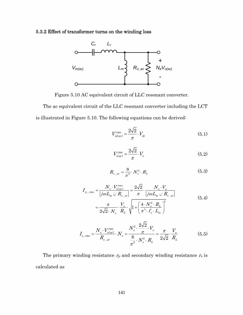
141
5.3.2 Effect of transformer turns on the winding loss
Ro_ac
LrCr
LmVin(ac) NeVo(ac)
+
-
Figure 5.10 AC equivalent circuit of LLC resonant converter.
The ac equivalent circuit of the LLC resonant converter including the LCT
is illustrated in Figure 5.10. The following equations can be derived:
( )
2 2rms
dcin acV V
(5.1)
o( )
2 2rms
oacV V
(5.2)
2
_ 2
8o ac e LR N R
(5.3)
( )
_
_ _
22
3
2 2
41
2 2
rms
e o ac e op rms
m o ac m o ac
o e L
L s me
N V N VI
j L R j L R
V N R
R f LN
(5.4)
2
( )
s_2_
2
2 2
8 2 2
rms e oe o ac o
rms e
o ac Le L
N VN V VI N
R RN R
(5.5)
The primary winding resistance rp and secondary winding resistance rs is
calculated as

142
acp p p
dc p
Rr l DCR
R
(5.6)
acs s s
dc s
Rr l DCR
R
(5.7)
where l represents winding length, DCR means the DC resistance, Rac/Rdc
implies the AC to DC resistance ratio. Combining (5.4) – (5.7), the primary and
secondary winding loss can be calculated as
2
_ _
22 22
2 2 3
41
8
p winding p rms p
o e L acp p
e L s m dc p
P I r
V N R Rl DCR
N R f L R
(5.8)
22
2
_winding _ 28o ac
s s rms s s s
L dc s
V RP I r l DCR
R R
(5.9)
It is clear that when primary turns np increase, Lm will increase. Therefore,
under same operating frequency condition, the primary coil current will
decrease. However, when primary turns increase, lp and ls will also increase,
which indicate that there is an optimal np that could achieve the lowest
winding loss. On the other hand, (5.4) indicates that higher operating
frequency will results in lower primary winding current, hence generates less
primary winding loss without the consideration of skin and proximity effects.
Figure 5.11 plots the total winding loss as a function of primary turns number
and operating frequency, based on the condition that coupling coefficient is 0.3,
input voltage and output voltage are both 20 V, and output current is 5 A.
Figure 5.11 indicates that under given circuit specification, the lowest winding

143
loss appears when primary turns number is about 4 ~ 7, and operating
frequency is around 700 ~ 1000 kHz range. If keep increasing fs, skin and
proximity effects would become more severe, hence the ac to dc resistance ratio
would rise drastically. Moreover, increase fs would results in higher driving
loss and switching loss in the circuit, hence reduce the overall efficiency.
Therefore, operating frequency should be set to a reasonably high value to
balance the trade-off between the winding current and winding resistance as
well as gate driver and MOSFETS switching loss.
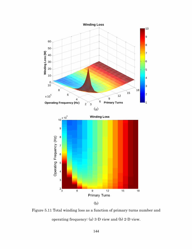
144
(a)
(b)
Figure 5.11 Total winding loss as a function of primary turns number and
operating frequency: (a) 3-D view and (b) 2-D view.
36
912
1518
2
4
6
8
10
x 105
0
10
20
30
40
50
60
Primary Turns
Winding Loss
Operating Frequency (Hz)
Win
din
g L
os
s (
W)
1
2
3
4
5
6
7
8
9
10

145
5.3.3 Effect of transformer turns on the core loss
Based on the fundamental theory of electromagnetism, the magnetic flux Φ
through a surface is the surface integral of the normal component of the
magnetic field intensity B passing through the surface, which can be presented
as
p pB S (5.10)
According to the faraday’s law of inductance, primary magnetic flux Φp can
be calculated as
p p r p m mn L I L I (5.11)
where
22
3
41
2o e L
p
e L s m
V N RI
N R f L
(5.12)
m4
dc
s m
VI
f L
(5.13)
For conventional tightly-coupled transformer, Lm is much larger than Lr,
Φp is mainly determined by Lm·Im. Increasing turns number while keeping
turns ratio same would reduce the flux swing Bp which is proportional to Φp,
hence reduce core loss. However, for loosely-coupled transformer, Lr is much
larger than Lm. In this case, increasing turns number while keeping coupling
and effective turns ratio same would not result in significant reduction of Ip.
Figure 5.12 demonstrates an example with 0.3 coupling coefficient, 500-kHz
operation, 20-V input voltage, 20-V output voltage, and 5-A output current
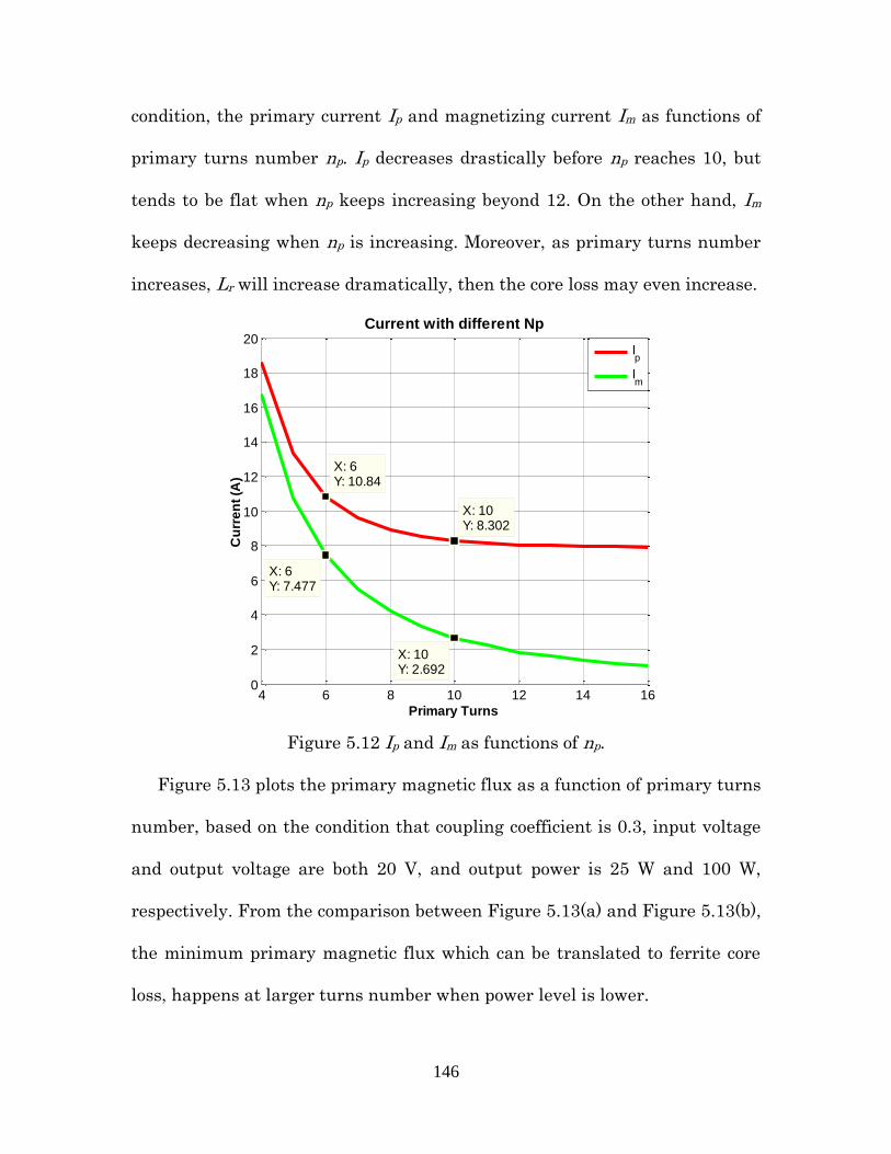
146
condition, the primary current Ip and magnetizing current Im as functions of
primary turns number np. Ip decreases drastically before np reaches 10, but
tends to be flat when np keeps increasing beyond 12. On the other hand, Im
keeps decreasing when np is increasing. Moreover, as primary turns number
increases, Lr will increase dramatically, then the core loss may even increase.
Figure 5.12 Ip and Im as functions of np.
Figure 5.13 plots the primary magnetic flux as a function of primary turns
number, based on the condition that coupling coefficient is 0.3, input voltage
and output voltage are both 20 V, and output power is 25 W and 100 W,
respectively. From the comparison between Figure 5.13(a) and Figure 5.13(b),
the minimum primary magnetic flux which can be translated to ferrite core
loss, happens at larger turns number when power level is lower.
4 6 8 10 12 14 160
2
4
6
8
10
12
14
16
18
20
X: 6Y: 10.84
Current with different Np
Primary Turns
Cu
rre
nt
(A)
X: 10Y: 8.302
X: 6Y: 7.477
X: 10Y: 2.692
Ip
Im
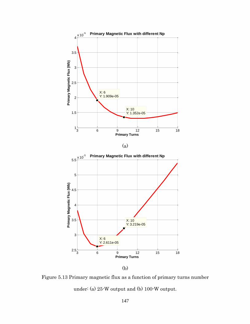
147
(a)
(b)
Figure 5.13 Primary magnetic flux as a function of primary turns number
under: (a) 25-W output and (b) 100-W output.
3 6 9 12 15 181
1.5
2
2.5
3
3.5
4x 10
-5
X: 6Y: 1.909e-05
Primary Magnetic Flux with different Np
Primary Turns
Pri
ma
ry M
ag
ne
tic
Flu
x (
Wb
)
X: 10Y: 1.352e-05
3 6 9 12 15 182.5
3
3.5
4
4.5
5
5.5x 10
-5
X: 6Y: 2.611e-05
Primary Magnetic Flux with different Np
Primary Turns
Pri
ma
ry M
ag
ne
tic
Flu
x (
Wb
)
X: 10Y: 3.219e-05

148
5.4 Experimental verification
In order to verify the proposed asymmetrical LCT design considerations
and efficiency improvement procedure based on turns number, a 100-W lab
prototype is built as shown in Figure 5.14. The input dc voltage is set at 20 V,
and the output dc voltage is regulated at 20 V, hence the full load output
current is 5 A. The switching devices Q1 ~ Q4 used for the primary high
frequency inverter are the OptiMOS BSC052N03LS from Infineon®, and the
secondary rectifier bridge D1 ~ D4 uses Schottky diode PDS1040L from Diodes®
Inc. Three 5PT46N103 capacitors from Electronic Concepts® are series
together to form a 3.33 nF resonant capacitor Cp.
Figure 5.14 Experimental setup on the bench.
5.4.1 Performance comparison between symmetrical and asymmetrical LCT
Two LCTs are implemented to compare the coupling coefficient and
compensation network efficiency when gap variation or misalignment occurs.
Both the LCT primary and secondary are made of NELD1050/44SNSN from
New England®, which is equivalent 14 AWG litz wire consisting of 1050

149
strands of 44 AWG wire. The 4 : 4 symmetrical LCT consists of primary and
secondary coils both with inner diameter 77 mm and outer diameter 95 mm.
Both primary and secondary winding resistance rp and rs for the symmetrical
LCT are around 35 mΩ. The 10 : 4 asymmetrical LCT comprises a transmitter
coil with 153 mm outer diameter and 110 mm inner diameter, and a receiver
coil with 95 mm outer diameter and 77 mm inner diameter. The transmitter
and receiver winding resistance are 135 mΩ and 35 mΩ, respectively. 12 pieces
of ferrite bars with material 3C94 are placed beneath the primary coil to help
shape the magnetic flux distribution and decrease radiated interference to
ambient environment. GW Instek LCR-821 digital LCR meter which has a
precision of 0.05% is used to measure the self and mutual inductances in order
to calculate the coupling coefficient.
Figure 5.15 shows the comparison between the measured and FEA
simulated coupling coefficient for different gap distance and misalignment
conditions for the symmetrical LCT. The experimental results agree well with
the simulated results. When the primary and secondary windings are perfectly
aligned, and the gap distance changes from 6 mm to 14 mm, the coupling
coefficient drops from 0.441 to 0.245, which represents 45% reduction. When
the gap is fixed at 10 mm, and the misalignment changes from 0 to 40 mm, the
coupling coefficient drops from 0.354 to 0.107, or 70% reduction.
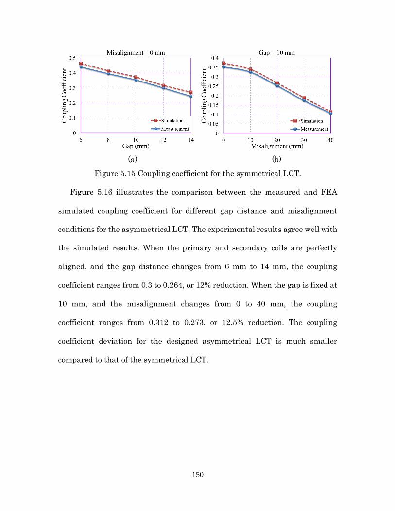
150
(a) (b)
Figure 5.15 Coupling coefficient for the symmetrical LCT.
Figure 5.16 illustrates the comparison between the measured and FEA
simulated coupling coefficient for different gap distance and misalignment
conditions for the asymmetrical LCT. The experimental results agree well with
the simulated results. When the primary and secondary coils are perfectly
aligned, and the gap distance changes from 6 mm to 14 mm, the coupling
coefficient ranges from 0.3 to 0.264, or 12% reduction. When the gap is fixed at
10 mm, and the misalignment changes from 0 to 40 mm, the coupling
coefficient ranges from 0.312 to 0.273, or 12.5% reduction. The coupling
coefficient deviation for the designed asymmetrical LCT is much smaller
compared to that of the symmetrical LCT.
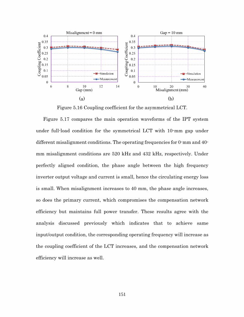
151
(a) (b)
Figure 5.16 Coupling coefficient for the asymmetrical LCT.
Figure 5.17 compares the main operation waveforms of the IPT system
under full-load condition for the symmetrical LCT with 10-mm gap under
different misalignment conditions. The operating frequencies for 0-mm and 40-
mm misalignment conditions are 520 kHz and 432 kHz, respectively. Under
perfectly aligned condition, the phase angle between the high frequency
inverter output voltage and current is small, hence the circulating energy loss
is small. When misalignment increases to 40 mm, the phase angle increases,
so does the primary current, which compromises the compensation network
efficiency but maintains full power transfer. These results agree with the
analysis discussed previously which indicates that to achieve same
input/output condition, the corresponding operating frequency will increase as
the coupling coefficient of the LCT increases, and the compensation network
efficiency will increase as well.

152
(a)
(b)
Figure 5.17 Main waveforms under full-load condition for the symmetrical
LCT with 10-mm gap and (a) 0-mm misalignment and (b) 40-mm
misalignment.
Figure 5.18 compares the full load efficiency between the symmetrical and
the asymmetrical LCT under different gap distance and misalignment
conditions. When the transmitter and receiver coils are in perfect aligned
position and the gap distance changes from 6 mm to 14 mm, the system
efficiency for the symmetrical and the asymmetrical LCT ranges from 88.56%

153
to 85.02% and 86.48% to 85.81%, respectively. When the gap is fixed at 10 mm,
and the misalignment increases from 0 to 40 mm, the system efficiency for the
symmetrical LCT drops from 87.5% to 70.9% due to a large primary side
current. With the asymmetrical LCT, however, the system efficiency stays
around 86% for the entire misalignment range. The efficiency results verify the
analysis in previous section, which indicates that higher coupling coefficient
results in higher compensation network efficiency. Moreover, with the
proposed asymmetrical LCT design, the coupling coefficient varies slightly
over the entire misalignment range, and thus the efficiency curve maintains
nearly flat. For real implementation, the system efficiency will suffer when put
under the metal chassis of the laptop, especially for low coupling conditions.
These effects can be mostly mitigated by adding some ferrite sheet on the top
of the receiver pad for the shielding purpose.
(a) (b)
Figure 5.18 Coupling coefficient for the asymmetrical LCT.
Figure 5.19 plots the operating frequency under different load and
misalignment conditions with the asymmetrical LCT. The figure indicates that

154
within 0 to 100 W and 0 to 40 mm misalignment range, the operating frequency
variation is less than 10 kHz, which will significantly ease the EMI design.
Figure 5.19 Operating frequency under different load and misalignment
conditions.
5.4.2 Performance evaluation between 6 : 2 and 10 : 4 LCT
With the designed asymmetrical LCT, the proposed design methodology to
improve LCT efficiency based on turns number need further evaluation.
Therefore, two LCTs with same geometry dimensions but different turns
number are built. GW Instek LCR-821 digital LCR meter which has a precision
of 0.05% is used to measure the self and mutual inductances in order to
calculate the coupling coefficient and effective turns ratio. The electrical
parameters for the two LCTs are described in Table 5-2.

155
Table 5-2 Parameters of two LCTs with different turns number
Parameters LCT#1 LCT#2
np : ns 6 : 2 10 : 4
Lr (µH) 13.22 28.74
Lm (µH) 1.30 2.83
kc 0.30 0.30
Ne 0.85 0.86
Figure 5.20 show the main operation waveforms of the IPT system under
full-load condition with two LCTs. The upper two traces indicate that the
primary active switches are turned on under ZVS condition as the current is
lagging the voltage. The lower two traces indicate that secondary diodes are
turned off under ZCS conditions as the zero current crossing point is in line
with the voltage transition point. Since both waveforms are captured under
full load condition, the RMS value of the secondary voltage vs and secondary
current is for both LCTs are almost identical. As analyzed in previous section,
with larger turns number, the magnetizing current im as well as primary
current ip will decrease, which matches with the RMS values of two currents
shown in Figure 5.20.

156
(a)
(b)
Figure 5.20 Main waveforms under full load condition for: (a) 6 : 2 LCT and
(b) 10 : 4 LCT.
The IPT system efficiency with two LCTs is plotted in Figure 5.21. At full
load condition, the efficiency of 6 : 2 LCT is slightly higher than that of 10 : 4.
However, the efficiency curve is more flat for 10 : 4 LCT, the efficiency
maintains higher than 86% from 20% load to full load.
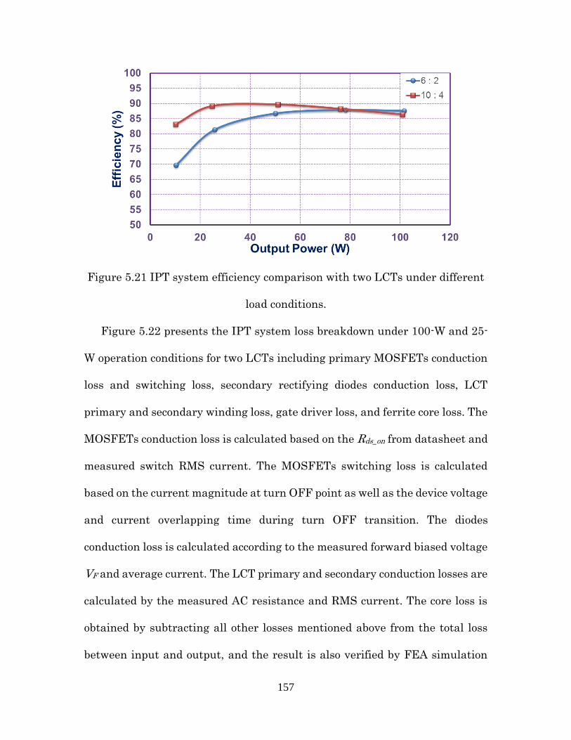
157
Figure 5.21 IPT system efficiency comparison with two LCTs under different
load conditions.
Figure 5.22 presents the IPT system loss breakdown under 100-W and 25-
W operation conditions for two LCTs including primary MOSFETs conduction
loss and switching loss, secondary rectifying diodes conduction loss, LCT
primary and secondary winding loss, gate driver loss, and ferrite core loss. The
MOSFETs conduction loss is calculated based on the Rds_on from datasheet and
measured switch RMS current. The MOSFETs switching loss is calculated
based on the current magnitude at turn OFF point as well as the device voltage
and current overlapping time during turn OFF transition. The diodes
conduction loss is calculated according to the measured forward biased voltage
VF and average current. The LCT primary and secondary conduction losses are
calculated by the measured AC resistance and RMS current. The core loss is
obtained by subtracting all other losses mentioned above from the total loss
between input and output, and the result is also verified by FEA simulation
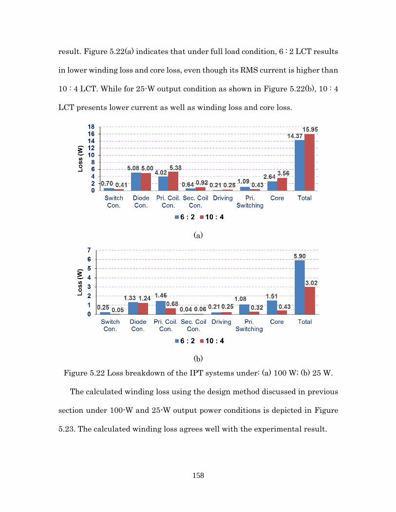
158
result. Figure 5.22(a) indicates that under full load condition, 6 : 2 LCT results
in lower winding loss and core loss, even though its RMS current is higher than
10 : 4 LCT. While for 25-W output condition as shown in Figure 5.22(b), 10 : 4
LCT presents lower current as well as winding loss and core loss.
(a)
(b)
Figure 5.22 Loss breakdown of the IPT systems under: (a) 100 W; (b) 25 W.
The calculated winding loss using the design method discussed in previous
section under 100-W and 25-W output power conditions is depicted in Figure
5.23. The calculated winding loss agrees well with the experimental result.

159
(a)
(b)
Figure 5.23 Calculated winding loss with different np under: (a) 100 W and
(b) 25 W
3 6 9 12 15 180
2
4
6
8
10
12
X: 6Y: 3.942
Winding Loss with different np
Primary Turns
Win
din
g L
os
s (
W)
X: 10Y: 5.352
Primary Winding Loss
Secondary Winding Loss
Total Winding Loss
3 6 9 12 15 180
0.5
1
1.5
2
2.5
3
X: 6Y: 1.381
Winding Loss with different np
Primary Turns
Win
din
g L
os
s (
W)
X: 10Y: 0.6181
Primary Winding Loss
Secondary Winding Loss
Total Winding Loss

160
5.5 Summary
This chapter demonstrates a LLC resonant converter based IPT system for
laptop charging. Several design considerations to reduce gap variation and
misalignment effects for the IPT system has been discussed. With the aid of
FEA simulation software, the flux distribution and coupling coefficient of the
transmitter and receiver coil with different dimension parameters can be
compared. Through the FEA simulation results and the corresponding
analysis, key design considerations can be drawn as follows:
An LCT with larger inner diameter primary coil tends to have a less
sensitive coupling coefficient when gap distance and misalignment
change. However, the averaged coupling coefficient is lower for this case.
When the inner diameter of secondary winding increases, the averaged
coupling coefficient will increase, but it is more sensitive to gap and
misalignment variations.
Once the optimized geometry of the LCT is attained, several design
considerations to further improve the IPT system efficiency can be drawn as
follows:
For given circuit specifications and LCT coupling conditions,
determination of the optimal primary winding turns number could help
achieve minimal winding loss and core loss.
For lower output power, the optimal primary winding turns number
tends to be larger compared to systems with a higher output power.

161
Increasing the operating frequency could help reduce the primary
current, but skin and proximity effects will dramatically increase the ac
resistance. Therefore, a reasonably high operating frequency should be
selected.
In order to validate the performance of the proposed design considerations
to increase the gap and misalignment tolerance, a 100-W hardware prototype
with a symmetrical LCT and the proposed asymmetrical LCT has been built
and tested. The experimental results demonstrate that the designed
asymmetrical LCT prototype maintains the coupling coefficient in a relatively
flat region. For example, under fully aligned condition, the coupling coefficient
varies from 0.3 to 0.264 when the gap increases from 6 to 14 mm. For the test
condition with 10-mm gap condition, the coupling coefficient varies from 0.312
to 0.273 when the misalignment varies from 0 to 40 mm. For comparison
purpose, the symmetrical LCT case would have coupling coefficient varying
from 0.354 to 0.107. With a relatively flat coupling coefficient under gap
variation and misalignment conditions, the system efficiency maintains nearly
flat over the entire test range. The maximum efficiency deviation with the
asymmetrical LCT is kept within 0.67% over the entire 40-mm misalignment
range. Again, for comparison purpose, the system efficiency with the
symmetrical LCT deviates 16.6% over the 40-mm misalignment range.
So as to evaluate the number of turns based loss estimation methodology,
two LCTs with same dimension but different number of turns are built. The

162
efficiency and loss breakdown of the prototype for each LCT configuration
agrees well with the design analysis. Under low power output condition, the 10
: 4 LCT presents higher efficiency owing to its relatively low magnetizing
current and primary winding current. However, under heavy load condition,
the superiority of primary winding current is not that significant, while the
winding length become dominant and hence hurts the system efficiency.

163
Chapter 6 Conclusions and Future Work
6.1 Conclusions
Recently, the concept of inductive power transmission has attracted a great
deal of interest in both academia and industry for its capability to make
charging easier for a lot of devices, from mobile phones to electric vehicles. The
advantages that an inductive power transfer system offers include
convenience, the lack of cable, no electric shock issue, capability to work under
some extreme environment, and so on. However, there are still many
significant drawbacks that have to be solved in order for these systems to reach
full functionality and compete with existing wired solutions: lower overall
efficiency, more sensitive to gap variation or misalignment condition, more
complicated design, safety and health threats from radiated electromagnetic
interference.
In order to solve the aforementioned issues that hinder the real
implementation of the IPT system, comprehensive analytical model for
individual part of and IPT system is discussed in detail. Since the major loss
of an IPT system is related to the winding conduction loss, full bridge inverter
is preferred owing to its moderate voltage and current stress. Half bridge
inverter is feasible when required output voltage is much lower than the input
voltage, in this case the secondary winding number can be reduced so as to
improve the system efficiency. Similarly on the receiver side, full-wave bridge
rectifier is more useful because of its modest voltage and current rating.

164
Although the center-tapped full-wave rectifier leads to lower conduction loss,
the difficulty of producing two symmetrical secondary winding becomes an
obstacle for its implementation in an IPT system. Voltage doubler is feasible
when required output voltage is much higher than the input voltage, in this
case the primary winding number can be reduced so as to improve the system
efficiency.
As the essential part in an IPT system, three equivalent models of the
loosely coupled transformer are introduced. The coupled inductor model and
the decoupled model are suitable for the analysis of IPT system with both sides
compensation. The lumped leakage inductance model, however, is favored for
resonant circuits with only primary side compensation. Five compensation
networks are introduced as SS, SP, PS, PP and LLC. Owing to the load and
coupling coefficient independency of SS configuration, it is considered to be
best suitable for inductive charging applications directly connected to the
battery. However, its relatively high voltage stress on the capacitors limits the
power transfer capability. LLC configuration doesn’t have any secondary
compensation capacitor, hence reduce the cost as well as room occupied in the
receiver side. Nevertheless, its relatively narrow voltage regulation capability
makes it more suitable for constant voltage output applications.
With detailed circuit model analysis as described above, the effect of the
resonant network parameters to the IPT system efficiency are investigated. A
novel compensation network parameters design methodology is proposed

165
based on multiple given requirement such as battery charging profile,
geometry constraints and operating frequency range, with the aim of avoiding
bifurcation phenomenon during the whole charging process and achieving
decent efficiency. A 4-kW hardware prototype including the LCT as well as the
compensation capacitors from the proposed design method is built and tested
under different gap and load conditions. Peak system DC-DC efficiencies of
98% and 96.6% are achieved with 4-cm and 8-cm air gap conditions, which are
comparable to the conventional plug-in type or wired charging systems for EVs.
A long-hour test with real EV batteries is conducted to verify the wireless
signal transmission and CC/CV mode seamless transition during the whole
charging profile.
In order to alleviate the gap variation or misalignment effect on the IPT
system coupling coefficient as well as efficiency, a novel LCT design approach
without additional complexity for the system is proposed. With the aid of FEA
simulation software, the flux distribution and coupling coefficient of the
transmitter and receiver coil with different dimension parameters can be
compared. An asymmetrical LCT based on the proposed design considerations
is built to compare with a traditional symmetrical LCT. With 10-mm gap and
0 to 40-mm misalignment, the coupling coefficient for the symmetrical LCT
drops from 0.354 to 0.107, and the corresponding efficiency decrease is 16.6%.
The operating frequency variation is nearly 100 kHz to maintain same
input/output condition. When employing the proposed asymmetrical LCT, the

166
coupling coefficient changes between 0.312 and 0.273, and the maximum
efficiency deviation is kept within 0.67% over the entire 40-mm misalignment
range. Moreover, the required frequency range to achieve same operation
condition is less than 10 kHz.
With the designed asymmetrical LCT geometry parameters, some design
considerations to further improve the IPT system efficiency are proposed. For
given circuit specifications and LCT coupling conditions, determination of the
optimal primary winding turns number could help achieve minimal winding
loss and core loss. For lower output power, the optimal primary winding turns
number tends to be larger compared to that for higher output power IPT
system. Two asymmetrical LCT with similar dimension but different number
of turns are built and tested with a 100-W hardware prototype for laptop
inductive charging. The winding loss and core loss from experimental results
match well with the analytical estimation. Under low power output condition,
the higher turns number LCT presents higher efficiency owing to its relatively
low magnetizing current and primary winding current. However, under heavy
load condition, the superiority of primary winding current is not that
significant, while the winding length become dominant and hence decreases
the system efficiency.
6.2 Future work
The research work in this dissertation demonstrates promising
performance in improving the efficiency and enhancing gap variation or

167
misalignment tolerance for the IPT system. However, there are other areas
where further investigations will be required to increase the overall
performance of the inductive coupling based CPT system. The following topics
are recommended for future work.
Multiple device charging
The proposed asymmetrical LCT configuration is tested with one
transmitter and one receiver. However, this concept can be extended to
charging multiple devices at the same time with some minor modification on
the LCT structure.
Dynamic vehicle charging
Owing to the high misalignment tolerance LCT design, the IPT system
efficiency can be maintained almost constant within desired misalignment
range. Therefore, multiple transmitter structure can be employed in order to
achieve dynamic vehicle charging with stable charging efficiency and
significantly reduce the battery capacity on-board.
Load recognition
A system with the ability to recognize the load should be implemented. By
analyzing thoroughly the current and the voltage of the primary coil, it should
be possible to avoid the activation of IPT system if a foreign object is placed on
transmitter. The electronic implementation and the digital control of such a
load recognition would be a great challenge.
Bidirectional IPT system

168
Bidirectional vehicle-to-grid (V2G) system has become an emerging topic in
recent years and similar concept should be adopted in the IPT system.
Therefore, further investigation is required to determine whether
bidirectionality could be achieved by using two back-to-back unidirectional IPT
systems or a designing a new topology that could implement bi-directionality.
Standard compliance
Although a lot of research has been performed to improve the performance
of the IPT system, their compliance to recently developed standards is always
overlooked. Due to the large gap between transmitter and receiver, radiated
EMI issue should draw further attention. The shielding technique without
hurting the efficiency too much would be a great challenge.
169
Reference
[1] “Ampère’s circuital law,” en.wikipedia.org/wiki/Ampère’s_circuital_law.
[2] M. N. O. Sadiku, Elements of Electromagnetics, Fourth ed. New York
(USA)/Oxford (UK): Oxford University Press, 1989.
[3] Boston University, “Applications of electromagnetic induction,”
physics.bu.edu/~duffy/py106/Electricgenerators.html.
[4] C. Wang, O. H. Stielau, and G. A. Covic, “Design considerations for a
contactless electric vehicle battery charger,” IEEE Transactions on
Industrial Electronics, vol. 52, no. 5, pp. 1308-1314, Oct. 2005.
[5] J. Sallan, J. Villa, A. Llombart, and J. Sanz, “Optimal Design of ICPT
Systems Applied to Electric Vehicle Battery Charge,” IEEE Transactions
on Industrial Electronics, vol. 56, no. 6, pp. 2140-2149, Jun. 2009.
[6] H. H. Wu, A. Gilchrist, K. D. Sealy, and D. Bronson, “A High Efficiency
5 kW Inductive Charger for EVs Using Dual Side Control,” IEEE
Transactions on Industrial Informatics, vol. 8, no. 3, pp. 585-595, Aug.
2012.
[7] G. A. Covic and J. T. Boys, “Modern Trends in Inductive Power Transfer
for Transportation Applications”, IEEE Journal of Emerging and
Selected Topics in Power Electronics, vol. 1, no. 1, pp. 28-41, Mar. 2013.
[8] S. M. Lukic, “Cutting the Cord, static and dynamic inductive wireless
charging of electric vehicles”, IEEE Electrification Magazine, vol. 1, no.
1, pp. 57-65, Sep. 2013.
170
[9] S. Lee, B. Choi, and C. T. Rim, “Dynamics Characterization of the
Inductive Power Transfer System for Online Electric Vehicles by Laplace
Phasor Transform,” IEEE Transactions on Power Electronics, vol. 28, no.
12, pp. 5902-5909, Dec. 2013.
[10] S. Y. Choi, B. W. Gu, S. W. Lee, W. Y. Lee, Jin Huh, C. T. Rim,
“Generalized Active EMF Cancel Methods for Wireless Electric Vehicles,”
IEEE Transactions on Power Electronics, vol. 29, no. 11, pp. 5770-5783,
Nov. 2014.
[11] C. Zheng, J.-S. Lai, R. Chen, W. E. Faraci, Z. U. Zahid, B. Gu, L. Zhang,
G. Lisi, and D. Anderson, “High-Efficiency Contactless Power Transfer
System for Electric Vehicle Battery Charging Application,” IEEE
Journal of Emerging and Selected Topics in Power Electronics, vol. 3,
no. 1, pp. 65-74, Mar. 2015.
[12] K. Chang-Gyun, S. Dong-Hyun, Y. Jung-Sik, P. Jong-Hu and B. H. Cho,
“Design of a contactless battery charger for cellular phone,” IEEE
Transactions on Industrial Electronics, vol. 48, no. 6, pp. 1238-1247, Dec.
2001.
[13] S. Y. R. Hui and W. W. C. Ho, “A new generation of universal contactless
battery charging platform for portable consumer electronic equipment, ”
IEEE Transactions on Power Electronics, vol. 20, no. 3, pp. 620-627, May.
2005.
171
[14] C.-H. Hu, C.-M. Chen, Y.-S. Shiao, T.-J. Chan and T.-R. Chen,
“Development of a universal contactless charger for handheld devices,”
in 2008 IEEE International Symposium on Industrial Electronics, 2008,
pp. 99-104.
[15] S. Y. Hui, “Planar wireless charging technology for portable electronic
products and Qi,” Proceedings of the IEEE, vol. 101, no. 6, pp. 1290-1301,
Jun. 2013.
[16] F. Sato, T. Nomoto, G. Kano, H. Matsuki and T. Sato, “A new contactless
powersignal transmission device for implanted functional electrical
stimulation (FES),” IEEE Transactions on Magnetics, vol. 40, no. 4, pp.
2964-2966, Apr. 2004.
[17] G. Wang, W. Liu, M. Sivaprakasam, and G. A. Kendir, “Design and
analysis of an adaptive transcutaneous power telemetry for biomedical
implants,” IEEE Transactions on Circuits and Systems I: Regular
Papers, vol. 52, no. 10, pp. 2109-2117, Oct. 2005.
[18] H. Miura, S. Arai, Y. Kakubari, F. Sato, H. Matsuki, and T. Sato,
“Improvement of the transcutaneous energy transmission system
utilizing ferrite cored coils for artificial hearts,” IEEE Transactions on
Magnetics, vol. 42, no. 10, pp. 3578-3580, Oct. 2006.
[19] K. Chen, Z. Yang, L. Hoang, J. Weiland, M. Humayun, and W. Liu, “An
integrated 256-channel epiretinal prosthesis,” IEEE Journal of Solid-
State Circuits, vol. 45, no. 9, pp. 1946-1956, Sep. 2010.

172
[20] A. Ram Rakhyani, S. Mirabbasi, and M. Chiao, “Design and optimization
of resonance-based efficient wireless power delivery systems for
biomedical implants,” IEEE Transactions on Biomedical Circuits and
Systems, vol. 5, no. 1, pp. 48-63, Feb. 2011.
[21] H. Cao, V. Landge, U. Tata, Y. Seo, S. Rao, S. J. Tang, H. F. Tibbals, S.
J. Spechler, and J.-C. Chiao, “An implantable, batteryless, and wireless
capsule with integrated impedance and pH sensors for gastroesophageal
reflux monitoring,” IEEE Transactions on Biomedical Engineering, vol.
59, no. 11, pp. 3131-3199, Nov. 2012.
[22] W. M. Ng, C. Zhang, D. Lin, and S. Y. Ron Hui, “Two- and Three-
Dimensional Omnidirectional Wireless Power Transfer,” IEEE
Transactions on Power Electronics, vol. 29, no. 9, pp. 4475-4478, Sep.
2014.
[23] R. Wu, W. Li, H. Luo, J. K. O. Sin, and C. C. Yue, “Design and
Characterization of Wireless Power Links for Brain-Machine Interface
Applications,” IEEE Transactions on Power Electronics, vol. 29, no. 10,
pp. 5462-5471, Oct. 2014.
[24] A. Tomar and S. Gupta, “Wireless power Transmission: Applications and
Components,” International Journal of Engineering Research &
Technology, vol. 1, no. 5, pp. 1-8, Jul. 2012.
[25] N. Shinohara, Wireless Power Transfer via Radiowaves, New York, NY,
USA: Wiley, 2014.
173
[26] “Heinrich Hertz,” en.wikipedia.org/wiki/Heinrich_Hertz.
[27] J. A. Angelo, Encyclopedia of Space and Astronomy, Facts on the file
Science library, New York, 2006.
[28] D. J. Cichon, W. Wiesbeck, “The Heinrich Hertz wireless experiments at
Karlsruhe in the view of modern communication,” in Proceedings of the
1995 International Conference on 100 Years of Radio, 1995, pp. 1-6.
[29] “Nikola Tesla,” en.wikipedia.org/wiki/Nikola_Tesla.
[30] “Tesla coil,” en.wikipedia.org/wiki/Tesla_coil.
[31] N. Tesla, “System of transmission of electrical energy,” U.S. Patent
645576 A, Mar. 20, 1900.
[32] N. Tesla, “The Problem of Increasing Human Energy,” Century
Magazine, Jun. 1990.
[33] N. Tesla, “The Transmission of Electrical Energy Without Wires as a
Means for Furthering Peace,” Electrical World and Engineer, pp. 21-24,
Jan. 1905.
[34] N. Tesla, “Apparatus for transmitting electrical energy,” U.S. Patent
1119732 A, Dec. 1, 1914.
[35] L. P. Wheeler, “II — Tesla’s contribution to high frequency,” Electrical
Engineering, vol. 62, no. 8, pp. 355-357, Aug. 1943.
[36] W. C. Brown, “The History of Power Transmission by Radio Waves,”
IEEE Transactions on Microwave Theory and Techniques, vol. 32, no.9,
pp. 1230-1242, Sep. 1984.

174
[37] W. C. Brown, “The history of wireless power transmission,” Solar Energy,
vol. 56, no. 1, pp. 3-21, Jan. 1996.
[38] M. Cheney, R. Uth, and J. Glenn, Tesla, Master of Lightning, Barnes &
Noble Publishing, 1999.
[39] N. Tesla, The Wireless Tesla, Wilder Publications, 2007.
[40] N. Tesla, Experiments with Alternate Currents of Very High Frequency
and Their Application to Methods of Artificial Illumination, Wilder
Publications, 2007.
[41] G. E. Leyh and M. D. Kennan, “Efficient wireless transmission of power
using resonators with coupled electric fields,” 40th North
American Power Symposium, 2008, pp. 1-4.
[42] W. C. Brown, “A survey of the elements of power transmission by
microwave beam,” in IRE International Conference, 1961, pages 93-105.
[43] W. C. Brown, J. F. Skowron, G. H. MacMaster, and J. W. Buckley, “The
super power CW amplitron,” in 1963 International Electron Devices
Meeting, 1963, vol. 9, pp. 52.
[44] J. F. Showrow, G. H. MacMaster, and W. C. Brown, “The super power
CW amplitron,” Microwave Journal, pp. 52, Oct 1964.
[45] P. E. Glaser, “Power from the Sun: Its Future,” Science, vol. 162, no.
3856, pp. 857-861, Nov. 1968.
175
[46] R. M. Dickinson, “Performance of a High-Power, 2.388-GHz Receiving
Array in Wireless Power Transmission Over 1.54 km,” in 1976 IEEE-
MTT-S International Microwave Symposium, 1976, pp. 139-141.
[47] W. C. Brown, “The Solar Power Satellite as a Source of Base Load
Electrical Power,” IEEE Transactions on Power Apparatus and Systems,
vol. PAS-100, no. 6, pp. 2766-2774, Jun. 1981.
[48] A. Fisher, “Beam-power plane,” Popular Science, pp. 62-65, Jan. 1988.
[49] W. C. Brown and E. E. Eves, “Beamed microwave power transmission
and its application to space,” IEEE Transactions on Microwave Theory
and Techniques, vol. 40, no. 6, pp. 1239-1250, Jun. 1992.
[50] H. Matsumoto, N. Kaya, I. Kimura, S. Miyatake, M. Nagatomo, and T.
Obayashi, “MINIX Project toward the Solar Power Satellites — Rocket
Experiment of Microwave Energy Transmission and Associated Plasma
Physics in The Ionosphere,” in ISAS Space Energy Symposium, 1986, pp.
69-76.
[51] H. Matsumoto and T. Kimura, “Nonlinear excitation of electron cyclotron
waves by a monochromatic strong microwave: computer simulation
analysis of the MINIX results,” Space Power, vol. 6, pp. 187-191, 1986.
[52] N. Kaya, H. Matsumoto, and R. Akiba, “Rocket experiment METS —
Microwave Energy Transmission in Space,” Space power, vol. 11, no. 3-4,
pp. 267-274, 1992.

176
[53] J. J. Schlesak, A. Alden, and T. Ohno, “A microwave powered high
altitude platform,” in IEEE MTT-S International Microwave Symposium
Digest, 1988, vol. 1, pp. 283-286.
[54] H. A. Bethe, R. Garwin, K. Gottfried, and H. W. Kendall, “Space-based
Ballistic-Missile Defense,” Scientific American, vol. 251, no. 4, pp. 39-49,
Oct. 1984.
[55] J. O. Dickey, P. L. Bender, J. E. Faller, X X Newhall, R. L. Ricklefs, J. G.
Ries, P. J. Shelus, C. Veillet, A. L. Whipple, J. R. Wiant, J. G. Williams,
and C. F. Yoder, “Lunar Laser Ranging: A Continuing Legacy of the
Apollo Program,” Science, vol. 265, no. 5171, pp. 482-490, Jul. 1994.
[56] D. L. Begley, “Relay Mirror Experiment,” in Proceedings of SPIE, 1996,
vol. 2699, pp. 192-197.
[57] F. Steinsiek, K. H. Weber, W. P. Foth, H. J. Foth, and C. Schäfer,
“Wireless power transmission experiment using an airship as relay
system and a moveable rover as ground target for later planetary
exploration missions,” in 8th ESA Workshop on Advanced Space
Technologies for Robotics and Automation, 2004, pp. 1-10.
[58] NASA, “NASA Research Team Successfully Flies First Laser-Powered
Aircraft,” www.nasa.gov/vision/earth/improvingflight/laser_plane.html.
[59] NASA, “NASA Armstrong Fact Sheet: Beamed Laser Power for UAVs,”
www.nasa.gov/centers/dryden/news/FactSheets/FS-087-DFRC.html.

177
[60] L. Bert and R. Puers, Omnidirectional Inductive Powering for Biomedical
Implants, Springer, 2008.
[61] K. Schuylenbergh and R. Puers, Inductive Powering: Basic Theory and
Application to Biomedical Systems, Springer, 2009.
[62] M. P. Theodoridis, “Effective Capacitive Power Transfer,” IEEE
Transactions on Power Electronics, vol. 27, no. 12, pp. 4906-4913, Dec.
2012.
[63] S. S. Valtchev, E. N. Baikova, and L. R. Jorge, “Electromagnetic Field as
the Wireless Transporter of Energy,” Facta Universitatis Series:
Electronics and Energetics, vol. 25, no. 3, pp. 171-181, Dec. 2012.
[64] M. Huschens, “Various techniques for wireless charging,” EETimes-Asia,
pp. 1-4, 2012.
[65] A. Gopinath, “All About Transferring Power Wirelessly,” Electronics For
You, vol. 2, no. 4, pp. 52-56, Aug. 2013.
[66] E. Sazonov and M. R. Neuman, Wearable Sensors: Fundamentals,
Implementation and Applications, Elsevier, 2014.
[67] C. Liu, A. P. Hu, G. A. Covic, and N. C.Nair, “Comparative Study of CCPT
Systems With Two Different Inductor Tuning Positions,” IEEE
Transactions on Power Electronics, vol. 27, no. 1, pp. 294-306, Jan. 2012.
[68] C. Liu, A. P. Hu, N. C. Nair, and G. A. Covic, “2-D alignment analysis of
capacitively coupled contactless power transfer systems,” in 2010 IEEE
Energy Conversion Congress and Exposition, 2010, pp. 652-657.

178
[69] M. Kline, I. Izyumin, B. Boser, and S. Sanders, “Capacitive power
transfer for contactless charging,” in 26th Annual IEEE Applied Power
Electronics Conference and Exposition, 2011, pp. 1398-1404.
[70] E. J. Nalos, W. W. Lund, O. Denman, and S. M. Rathjen, “Microwave
Power Beaming for Long Range Energy Transfer,” in 8th European
Microwave Conference, 1978, pp. 573-578.
[71] J. D. L. S. Luk, A. Celeste, P. Romanacce, L. C. K. Sang, and J. C. Gatina,
“Point-to-point wireless power transportation in reunion island,” in 48th
International Astronautical Congress, 1997.
[72] A. Massa, G. Oliveri, F. Viani, and P. Rocca, “Array Designs for Long-
Distance Wireless Power Transmission: State-of-the-Art and Innovative
Solutions,” Proceedings of the IEEE, vol. 101, no. 6, pp. 1464-1481, Jun.
2013.
[73] M. A. Stuchly, “Health effects of exposure to electromagnetic fields,” in
1995 IEEE Aerospace Applications Conference, 1995, pp. 351-368.
[74] G. A. Landis, “Moonbase night power by laser illumination,” Journal of
Propulsion and Power, vol. 8, no. 1, pp. 251-254, Jan.-Feb.1992.
[75] G. A. Landis, “Applications for space power by laser transmission,” in
Proceedings of SPIE, 1994, vol. 2121, pp. 252-255.
[76] L. Summerer and O. Purcell. “Concepts for wireless energy transmission
via laser,” Europeans Space Agency - Advanced Concepts Team, 2009.

179
[77] A. Sahai, D. Graham, “Optical wireless power transmission at long
wavelengths,” in 2011 International Conference on Space Optical
Systems and Applications, 2011, pp. 164-170.
[78] M. Weksler and J. Shwartz, “Solar-pumped solid-state lasers,” IEEE
Journal of Quantum Electronics, vol. 24, no. 6, pp.1222-1228, Jun. 1988.
[79] D. Smith, “Wireless power spells end for cables,”
www.theguardian.com/science/2009/jan/04/wireless-power-technology-
witricity.
[80] R. M. Dickinson, “Wireless power transmission technology state of the
art the first Bill Brown lecture.” Acta Astronautica, vol. 53, no. 4, pp. 561-
570, 2003.
[81] S. Sasaki and K. Tanaka, “Wireless power transmission technologies for
solar power satellite,” in 2011 IEEE MTT-S International Microwave
Workshop Series on Innovative Wireless Power Transmission:
Technologies, Systems, and Applications, 2011, pp. 3-6.
[82] R. Dickinson and J. Grey, “Lasers for wireless power transmission,” Jet
Propulsion Laboratory and AIAA Technical Report, 1999.
[83] S. S. Mohammed and K. Ramasamy, “Solar Power Generation using SPS
and Wireless Power Transmission,” in Proceeding of international
Conference on Energy and Environment, 2009, pp. 413-418.
[84] E. B. Tarrson, “Electric toothbrush which is rechargeable with or without
a recharging stand,” U.S. Patent 3379952 A, Apr. 23, 1968.

180
[85] R. G. Holmes, “Separable transformer battery charger,” U.S. Patent
3418552 A, Dec. 24, 1968.
[86] T. Klinger, M. Pachel, M. Sonnek, and E. Krammer, “Electric
toothbrush,” U.S. Patent 5561881 A, Oct. 8, 1996.
[87] H. Abe, H. Sakamoto, and K. Harada, “A noncontact charger using a
resonant converter with parallel capacitor of the secondary coil,” IEEE
Transactions on Industry Applications, vol. 36, no. 2, pp. 444-451, Mar.-
Apr. 2000.
[88] B. Choi and J. Nho, “Contactless energy transfer using planar printed
circuit board windings,” Electronics Letters, vol. 37, no. 16, pp. 1007-
1009, Aug. 2001.
[89] B. Choi, J. Nho, H. Cha, T. Ahn, and S. Choi, “Design and
implementation of lowprofile contactless battery charger using planar
printed circuit board windings as energy transfer device,” IEEE
Transactions on Industrial Electronics, vol. 51, no. 1, pp. 140-147, Feb.
2004.
[90] S. Y. R. Hui and W. W. C. Ho, “A new generation of universal contactless
Battery Charging platform for portable Consumer Electronic
equipment,” IEEE Transactions on Power Electronics, vol. 20, no. 3, pp.
620-627, May 2005.
[91] X. Liu and S. Y. R. Hui, “Equivalent Circuit Modeling of a Multilayer
Planar Winding Array Structure for Use in a Universal Contactless
181
Battery Charging Platform,” IEEE Transactions on Power Electronics,
vol. 22, no. 1, pp. 21-29, Jan. 2007.
[92] X. Liu and S. Y. R. Hui, “Simulation Study and Experimental Verification
of a Universal Contactless Battery Charging Platform With Localized
Charging Features,” IEEE Transactions on Power Electronics, vol. 22,
no. 6, pp. 2202-2210, Nov. 2007.
[93] X. Liu and S. Y. R. Hui, “Optimal Design of a Hybrid Winding Structure
for Planar Contactless Battery Charging Platform,” IEEE Transactions
on Power Electronics, vol. 23, no. 1, pp. 455-463, Jan. 2008.
[94] Y. Su, X. Liu, and S. Y. R. Hui, “Mutual Inductance Calculation of
Movable Planar Coils on Parallel Surfaces,” IEEE Transactions on Power
Electronics, vol. 24, no. 4, pp. 1115-1123, Apr. 2009.
[95] W. X. Zhong, X. Liu, and S. Y. R. Hui, “A Novel Single-Layer Winding
Array and Receiver Coil Structure for Contactless Battery Charging
Systems With Free-Positioning and Localized Charging Features,” IEEE
Transactions on Industrial Electronics, vol. 58, no. 9, pp. 4136-4144, Sep.
2011.
[96] W. X. Zhong, C. Zhang, X. Liu, and S. Y. R. Hui, “A Methodology for
Making a Three-Coil Wireless Power Transfer System More Energy
Efficient Than a Two-Coil Counterpart for Extended Transfer Distance,”
IEEE Transactions on Power Electronics, vol. 30, no. 2, pp. 933-942, Feb.
2015.

182
[97] “Splashpower,” en.wikipedia.org/wiki/Splashpower.
[98] “Splashpower powers mobile phones without chargers,”
www.esato.com/archive/t.php/t-131342,1.html.
[99] EE Times, “Splashpower to make bigger wireless splash at Fulton
Innovation,” www.eetimes.com/document.asp?doc_id=1250844.
[100] http://ecoupled.com/
[101] D. W. Baarman, “Adaptive inductive power supply with communication,”
U.S. Patent 7522878 B2, Apr. 21, 2009.
[102] “Fulton Innovation to present wirelessly powered laptop at CES 2008,”
ecoupled.com/content/fulton-innovation-present-wirelessly-powered-
laptop-ces-2008.
[103] “Palm Pre,” en.wikipedia.org/wiki/Palm_Pre.
[104] “Palm Touchstone gets taken apart on the FCC,”
www.wirelessgoodness.com.
[105] “Induction charging backs for the Pre, Pixi pass through the FCC as
well,” www.wirelessgoodness.com.
[106] “Palm, Inc.,” en.wikipedia.org/wiki/Palm,_Inc.
[107] “Powermat,” powermat.com.
[108] “WiPower,” www.qualcomm.com/products/wipower.
[109] “Jolt Charger,” www.joltcharger.com.
[110] “VÜ Wireless Charger,” tylt.com/vu.
183
[111] A. Esser, “Contactless charging and communication for electric vehicles”,
IEEE Industrial Applications Magazine, vol. 1, no. 6, pp. 4-11, Nov.-Dec.
1995.
[112] H. Sakamoto, K. Harada, S. Washimiya, K. Takehara, and F. Nakao,
“Large air-gap coupler for inductive charger,” IEEE Transactions on
Magnetics, vol. 35, no. 5, pp. 3526-3528, Sep. 1999.
[113] M. Hutin and M. LeBlanc, “Transformer system for electric railways,”
U.S. Patent 527857 A, Oct. 23, 1894.
[114] Systems Control Technology, Inc., “Roadway Powered Electric Vehicle
Project Track Construction and Testing Program Phase 3D,” California
Partners for Advanced Transit and Highways (PATH) Research Report,
1994.
[115] “Magne Charge,” en.wikipedia.org/wiki/Magne_Charge.
[116] “EV1 Club,” www.eanet.com/ev1-club.
[117] F. Musavi, M. Edington, and W. Eberle, “Wireless power transfer: A
survey of EV battery charging technologies,” in 2012 IEEE Energy
Conversion Congress and Exposition, 2012, pp. 1804-1810.
[118] A. W. Green and J. T. Boys, “10 kHz inductively coupled power transfer-
concept and control,” in 5th International Conference on Power
Electronics and Variable-Speed Drives, 1994, pp. 694-699.

184
[119] O. H. Stielau and G. A. Covic, “Design of loosely coupled inductive power
transfer systems,” in 2000 International Conference on Power System
Technology, 2000, vol. 1, pp. 85-90.
[120] C.-S. Wang, O. H. Stielau, and G. A. Covic, “Design considerations for a
contactless electric vehicle battery charger,” IEEE Transactions on
Industrial Electronics, vol. 52, no. 5, pp. 1308-1314, Oct. 2005.
[121] M. Budhia, J. T. Boys, G. A. Covic, and C.-Y. Huang, “Development of a
Single-Sided Flux Magnetic Coupler for Electric Vehicle IPT Charging
Systems,” IEEE Transactions on Industrial Electronics, vol. 60, no. 1, pp.
318-328, Jan. 2013.
[122] “WEVC Trials,” www.qualcommhalo.com/index.php/wevc-trials.
[123] “WiTricity,” witricity.com.
[124] A. Kurs, A. Karalis, R. Moffatt, J. D. Joannopoulos, P. Fisher, and M.
Soljačić, “Wireless power transfer via strongly coupled magnetic
resonances,” Science, vol. 317, no. 5834, pp. 83-86, Jul. 2007.
[125] A. Karalis, J. D. Joannopoulos, and M. Soljačić, “Efficient wireless non-
radiative mid-range energy transfer,” Annals of Physics, vol. 323, no. 1,
pp. 34-48, Jan. 2008.
[126] J. M. Miller, “Wireless plug-in electric vehicle (PEV) charging.” In 2012
US DOE hydrogen and fuel cell programs and vehicle technologies
program annual merit review and peer evaluation meeting, 2012.

185
[127] J. M. Miller, C. P. White, O. C. Onar, and P. M. Ryan, “Grid side
regulation of wireless power charging of plug-in electric vehicles,” in 2012
IEEE Energy Conversion Congress and Exposition, 2012, pp. 261-268.
[128] O. C. Onar, J. M. Miller, S. L. Campbell, C. Coomer, C. P. White, L. E.
Seiber, “A novel wireless power transfer for in-motion EV/PHEV
charging,” in 28th Annual IEEE Applied Power Electronics Conference
and Exposition, 2013, pp. 3073-3080.
[129] J. M. Miller, O. C. Onar, C. P. White, S. L. Campbell, C. Coomer, L. E.
Seiber, R. Sepe, and A. Steyerl, “Demonstrating Dynamic Wireless
Charging of an Electric Vehicle: The Benefit of Electrochemical Capacitor
Smoothing,” IEEE Power Electronics Magazine, vol. 1, no. 1, pp. 12-24,
Mar. 2014.
[130] “Plugless,” pluglesspower.com.
[131] K. Thibaut, “Google Is Hooking Up Their Employees With Plugless
Power For Their Electric Cars (Video),” techcrunch.com.
[132] P. Bacque, “Evatran to begin shipping its Plugless electric vehicle
charging system,” www.richmond.com.
[133] “OLEV Technologies,” olevtech.com.
[134] S. Lee, J. Huh, C. Park, N.-S. Choi, G.-H. Cho, and C.-T. Rim, “On-Line
Electric Vehicle using inductive power transfer system,” in 2010 IEEE
Energy Conversion Congress and Exposition, 2010, pp. 1598-1601.

186
[135] S. Ahn and J. Kim, “Magnetic field design for high efficient and low EMF
wireless power transfer in on-line electric vehicle,” in Proceedings of the
5th European Conference on Antennas and Propagation, 2011, pp. 3979-
3982.
[136] J. Huh, S.-W. Lee, W.-Y. Lee, G.-H. Cho, and C.-T. Rim, “Narrow-width
inductive power transfer system for online electrical vehicles,” IEEE
Transactions on Power Electronics, vol. 26, no. 12, pp. 3666-3679, Dec.
2011.
[137] “PRIMOVE,” primove.bombardier.com.
[138] P. Albexon, “Bombardier PRIMOVE, catenary-free operation,” in
AusRAIL PLUS 2009, 2009.
[139] Transportation, Bombardier, “PRIMOVE contactless and catenary-free
operation,” EcoActive Technologies, 2010.
[140] “Wireless Power Consortium,” www.wirelesspowerconsortium.com.
[141] “Power Matters Alliance,” www.powermatters.org.
[142] “Alliance for Wireless Power,” www.rezence.com.
[143] “Alliance for Wireless Power and Power Matters Alliance Agree to
Merge,” www.rezence.com/media/news/alliance-wireless-power-and-
power-matters-alliance-agree-merge.
[144] Mouser Electronics, “The Direction of Wireless Charging
Technology,” www.mouser.com/applications/wireless-charging-direction.

187
[145] Würth Elektronik, “Is flexible material the future of WPT?” in 30th
Annual IEEE Applied Power Electronics Conference and Exposition,
2015.
[146] J. Schneider, “SAE J2954 Overview and Path Forward,” www.sae.org.
[147] “Induction heating,” en.wikipedia.org/wiki/Induction_heating.
[148] V. Rudnev, D. Loveless, R. L. Cook, and M. Black, Handbook of Induction
Heating, CRC Press, 2002.
[149] “Induction cooking,” en.wikipedia.org/wiki/Induction_cooking.
[150] Z. Liu, “High Frequency Inverter Power Stage Design Considerations for
Non-Magnetic Materials Induction Cooking,” Master thesis, Bradley
Department of Electrical and Computer Engineering, Virginia Tech,
Blacksburg, VA, 2011.
[151] S. Nagai, H. Nagura, M. Nakaoka, and A. Okuno, “High-frequency
inverter with phase-shifted PWM and load-adaptive PFM control
strategy for industrial induction-heating”, in 1993 IEEE Industry
Applications Society Annual Meeting, 1993, vol. 3, pp. 2165-2172.
[152] M. Kamli, S. Yamamoto, and M. Abe, “A 50-150 kHz half-bridge inverter
for induction heating applications”, IEEE Transactions on Industrial
Electronics, vol. 43, no. 1, pp. 163-172, Feb. 1996.
[153] O. Lucia, J. M. Burdio, I. Millan, J. Acero, and D. Puyal, “Load-Adaptive
Control Algorithm of Half-Bridge Series Resonant Inverter for Domestic

188
Induction Heating,” IEEE Transactions on Industrial Electronics, vol. 56,
no. 8, pp. 3106-3116, Aug. 2009.
[154] H. W. Koertzen, J. D. V. Wyk, and J. A. Ferreira, "Design of the half-
bridge, series resonant converter for induction cooking," in 26th Annual
IEEE Power Electronics Specialists Conference, 1995, vol. 2, pp. 729-735.
[155] B.-K. Lee, J.-W. Jung, B.-S. Suh, and D.-S. Hyun, “A new half-bridge
inverter topology with active auxiliary resonant circuit using insulated
gate bipolar transistors for induction heating applications,” in 28th
Annual IEEE Power Electronics Specialists Conference, 1997, vol. 2, pp.
1232-1237.
[156] “Induction furnace,” en.wikipedia.org/wiki/Induction_furnace.
[157] “Induction welding,” en.wikipedia.org/wiki/Induction_welding.
[158] H. Raillard, “Development of an implantable cardiac pacemaker,” in 1962
IEEE International Solid-State Circuits Conference, 1962, pp. 88-89.
[159] A. C. Hoogerwerf and K. D. Wise, “A three-dimensional microelectrode
array for chronic neural recording,” IEEE Transactions on Biomedical
Engineering, vol. 41, no. 12, pp. 1136-1146, Dec. 1994.
[160] W. Mokwa, “Medical implants based on microsystems,” Measurement
Science and Technology, vol. 18, no. 5, pp. 47-57, May 2007.
[161] M. Soma, Douglas C. Galbraith, and R. L. White, “Radio-Frequency Coils
in Implantable Devices: Misalignment Analysis and Design Procedure,”
189
IEEE Transactions on Biomedical Engineering, vol. 34, no. 4, pp.276-282,
Apr. 1987.
[162] G. B. Joung and B. H. Cho, “An energy transmission system for an
artificial heart using leakage inductance compensation of
transcutaneous transformer,” IEEE Transactions on Power Electronics,
vol. 13, pp. 1013-1022, Nov. 1998.
[163] F.-G. Zeng, S. Rebscher, W. Harrison, X. Sun, and H. Feng, “Cochlear
Implants: System Design, Integration, and Evaluation,” IEEE Reviews
in Biomedical Engineering, vol. 1, pp. 115-142, 2008.
[164] P. Shenoy, K. J. Miller, B. Crawford, R. P. N. Rao, “Online
Electromyographic Control of a Robotic Prosthesis,” IEEE Transactions
on Biomedical Engineering, vol. 55, no. 3, pp. 1128-1135, Mar. 2008.
[165] P. Si, A. P. Hu, S. Malpas, and D. Budgett, “A Frequency Control Method
for Regulating Wireless Power to Implantable Devices,” IEEE
Transactions on Biomedical Circuits and Systems, vol. 2, no. 1, pp. 22-
29, Mar. 2008.
[166] S. Smith, “An implantable drug delivery system with wireless power and
communication,” in 2009 IET Bionic Health: Next Generation Implants,
Prosthetics and Devices, 2009, pp. 1-88.
[167] Y.-K. Song, D. A. Borton, S. Park, W. R. Patterson, C. W. Bull, F.
Laiwalla, J. Mislow, J. D. Simeral, J. P. Donoghue, and A. V. Nurmikko,
“Active Microelectronic Neurosensor Arrays for Implantable Brain

190
Communication Interfaces,” IEEE Transactions on Neural Systems and
Rehabilitation Engineering, vol. 17, no. 4, pp. 339-345, Aug. 2009.
[168] D. B. Shire, S. K. Kelly, J. Chen, P. Doyle, M. D. Gingerich, S. F. Cogan,
W. A. Drohan, O. Mendoza, L. Theogarajan, J. L. Wyatt, and J. F. Rizzo,
“Development and Implantation of a Minimally Invasive Wireless
Subretinal Neurostimulator,” IEEE Transactions on Biomedical
Engineering, vol. 56, no. 10, pp. 2502-2511, Oct. 2009.
[169] B. K. Thurgood, D. J. Warren, N. M. Ledbetter, G. A. Clark, and R. R.
Harrison, “A Wireless Integrated Circuit for 100-Channel Charge-
Balanced Neural Stimulation,” IEEE Transactions on Biomedical
Circuits and Systems, vol. 3, no. 6, pp. 405-414, Dec. 2009.
[170] V. Chawla, D. S. Ha, “An overview of passive RFID,” IEEE
Communications Magazine, vol. 45, no. 9, pp. 11-17, Sep. 2007.
[171] S. C. Q. Chen and V. Thomas, “Optimization of inductive RFID
technology,” in Proceedings of the 2001 IEEE International Symposium
on Electronics and the Environment, 2001, pp. 82-87.
[172] M. Philipose, J. R. Smith, B. Jiang, A. Mamishev, S. Roy, and K.
Sundara-Rajan, “Battery-free wireless identification and sensing,” IEEE
Pervasive Computing, vol. 4, no. 1, pp. 37-45, Jan.-Mar. 2005.
[173] K. R. Foster, J. Jaeger, “RFID Inside,” IEEE Spectrum, vol. 44, no. 3, pp.
24-29, Mar. 2007.

191
[174] P. Sorrells, “Passive RFID Basics,” Application Note AN680, Microchip
Technology, 1998.
[175] R. Weinstein, “RFID: a technical overview and its application to the
enterprise,” IT Professional, vol. 7, no. 3, pp. 27-33, May-Jun. 2005.
[176] K. V. S. Rao, P. V. Nikitin, and S. F. Lam, “Antenna design for UHF RFID
tags: a review and a practical application,” IEEE Transactions on
Antennas and Propagation, vol. 53, no. 12, pp. 3870-3876, Dec. 2005.
[177] N. O. Sokal and A. D. Sokal, “Class E-A new class of high-efficiency tuned
single-ended switching power amplifiers,” IEEE Journal of Solid-State
Circuits, vol. 10, no. 3, pp. 168-176, Jun. 1975.
[178] F. H. Raab, “Effects of circuit variations on the class E tuned power
amplifier,” IEEE Journal of Solid-State Circuits, vol. 13, no. 2, pp. 239-
247, Apr. 1978.
[179] N. O. Sokal, “Class E high-efficiency power amplifiers, from HF to
microwave,” in 1998 IEEE MTT-S International Microwave Symposium
Digest, 1998, vol. 2, pp. 1109-1112.
[180] M. Kazimierczuk, “Collector amplitude modulation of the class E tuned
power amplifier,” IEEE Transactions on Circuits and Systems, vol. 31,
no. 6, pp. 543-549, Jun. 1984.
[181] G. A. Kendir, W. Liu, G. Wang, M. Sivaprakasam, R. Bashirullah, M. S.
Humayun, and J. D. Weiland, “An optimal design methodology for
inductive power link with class-E amplifier,” IEEE Transactions on

192
Circuits and Systems I: Regular Papers, vol. 52, no. 5, pp. 857-866, May
2005.
[182] J. J. Casanova, Z. N. Low, and J. Lin, “Design and Optimization of a
Class-E Amplifier for a Loosely Coupled Planar Wireless Power
System,” IEEE Transactions on Circuits and Systems II: Express Briefs,
vol. 56, no. 11, pp. 830-834, Nov. 2009.
[183] E. M. Thomas, J. D. Heebl, C. Pfeiffer, and A. Grbic, “A Power Link Study
of Wireless Non-Radiative Power Transfer Systems Using Resonant
Shielded Loops,” IEEE Transactions on Circuits and Systems I: Regular
Papers, vol. 59, no. 9, pp. 2125-2136, Sept. 2012.
[184] L. Chen, S. Liu, Y. C. Zhou, and T. J. Cui, “An Optimizable Circuit
Structure for High-Efficiency Wireless Power Transfer,” IEEE
Transactions on Industrial Electronics, vol. 60, no. 1, pp. 339-349, Jan.
2013.
[185] M. Pinuela, D. C. Yates, S. Lucyszyn, and P. D. Mitcheson, “Maximizing
DC-to-Load Efficiency for Inductive Power Transfer,” IEEE Transactions
on Power Electronics, vol. 28, no. 5, pp. 2437-2447, May 2013.
[186] A. Khaligh and Z. Li, “Battery, Ultracapacitor, Fuel Cell, and Hybrid
Energy Storage Systems for Electric, Hybrid Electric, Fuel Cell, and
Plug-In Hybrid Electric Vehicles: State of the Art,” IEEE Transactions
on Vehicular Technology, vol. 59, no. 6, pp. 2806-2814, Jul. 2010.

193
[187] “SAE Electric Vehicle and Plug in Hybrid Electric Vehicle Conductive
Charge Coupler,” standards.sae.org/wip/j1772.
[188] M. Eghtesadi, “Inductive power transfer to an electric vehicle-analytical
model,” in IEEE 1990 Vehicular Technology Conference, 1990, pp. 100-
104.
[189] D. Pedder, A. Brown, and J. Skinner, “A contactless electrical energy
transmission system,” IEEE Transactions on Industrial Electronics, vol.
46, no. 1, pp. 23-30, Feb. 1999.
[190] R. Laouamer, M. Brunello, J. Ferrieux, O. Normand, and N. Buchheit, “A
multi-resonant converter for non-contact charging with electromagnetic
coupling,” in 1997 Industrial Electronics, Control and Instrumentation
International Conference, 1997, vol. 2, pp. 792-797.
[191] K. Kobayashi, N. Yoshida, Y. Kamiya, Y. Daisho, and S. Takahashi,
“Development of a non-contact rapid charging inductive power supply
system for electric-driven vehicles,” in 2010 IEEE Vehicle Power and
Propulsion Conference, 2010, pp. 1-6.
[192] Y. Nagatsuka, N. Ehara, Y. Kaneko, S. Abe, and T. Yasuda, “Compact
contactless power transfer system for electric vehicles,” in 2010
International Power Electronics Conference, 2010, pp. 807-813.
[193] S. Judek, and K. Karwowski, “Supply of electric vehicles via magnetically
coupled air coils,” in 2008 Power Electronics and Motion Control
Conference, 2008, pp. 1497-1504.

194
[194] H. Bai, A. Taylor, W. Guo, G. Szatmari-Voicu, N. Wang, J. Patterson, and
J. Kane, “Design of an 11 kW power factor correction and 10 kW ZVS
DC/DC converter for a high-efficiency battery charger in electric
vehicles,” IET Power Electronics, vol. 5, no. 9, pp. 1714-1722, Nov. 2012.
[195] B. Gu, J.-S. Lai, N. Kees, and C. Zheng, “Hybrid-Switching Full-Bridge
DC-DC Converter With Minimal Voltage Stress of Bridge Rectifier,
Reduced Circulating Losses, and Filter Requirement for Electric Vehicle
Battery Chargers,” IEEE Transactions on Power Electronics, vol. 28, no.
3, pp. 1132-1144, Mar. 2013.
[196] C.-S. Wang, G. A. Covic, and O. H. Stielau, “Power transfer capability
and bifurcation phenomena of loosely coupled inductive power transfer
systems,” IEEE Transactions on Industrial Electronics, vol. 51, no. 1, pp.
148-157, Feb. 2004.
[197] A. Feng, H. Qin, Z. Mao, and P. Peng, “Analysis of Bifurcation
Phenomena Based on Optimized Transformer in Loosely Coupled
Inductive Power Transfer System,” in 2010 International Conference on
Electrical and Control Engineering, 2010, pp. 3324-3327.
[198] “T-145 Data Sheet,” www.trojanbattery.com.
[199] “nRF24L01+,” www.nordicsemi.com.
[200] A. K. RamRakhyani and G. Lazzi, “Multicoil Telemetry System for
Compensation of Coil Misalignment Effects in Implantable Systems,”

195
IEEE Antennas and Wireless Propagation Letters, vol. 11, pp. 1675-
1678, 2012.
[201] K. Mori, L. Hyunkeun, S. Iguchi, K. Ishida, M. Takamiya, and T. Sakurai,
“Positioning-Free Resonant Wireless Power Transmission Sheet With
Staggered Repeater Coil Array (SRCA),” IEEE Antennas and Wireless
Propagation Letters, vol. 11, pp. 1710-1713, 2012.
[202] J. P. C. Smeets, T. T. Overboom, J. W. Jansen, and E. A. Lomonova,
“Comparison of positionindependent contactless energy transfer
systems,” IEEE Transactions on Power Electronics, vol. 28, no. 4, pp.
2059-2067, Apr. 2013.
[203] H. R. Ahn, M. S. Kim, and Y. J. Kim, “Inductor array for minimising
transfer efficiency decrease of wireless power transmission components
at misalignment,” Electronics Letters, vol. 50, no. 5, pp. 393-394, Feb.
2014.
[204] M. L. G. Kissin, C. Y. Huang, G. A. Covic, and J. T. Boys, “Detection of
the tuned point of a fixed-frequency LCL resonant power supply,” IEEE
Transactions on Power Electronics, vol. 24, no. 4, pp. 1140-1143, Apr.
2009.
[205] H. Wu, G. Covic, J. Boys, and D. Robertson, “A series-tuned
inductivepower- transfer pickup with a controllable AC-voltage output,”
IEEE Transactions on Power Electronics, vol. 26, no. 1, pp. 98-109, Jan.
2011.
196
[206] J. L. Villa, J. Sallan, J. F. Sanz Osorio, and A. Llombart, “High-
Misalignment Tolerant Compensation Topology For ICPT Systems,”
IEEE Transactions on Industrial Electronics, vol. 59, no. 2, pp. 945-951,
Feb. 2012.
[207] S. Aldhaher, P. C.-K. Luk, and J. F. Whidborne, “Tuning Class E
Inverters Applied in Inductive Links Using Saturable Reactors,” IEEE
Transactions on Power Electronics, vol. 29, no. 6, pp. 2969-2978, Jun.
2014.
[208] Y. Lim, H. Tang, S. Lim, and J. Park, “An Adaptive Impedance-Matching
Network Based on a Novel Capacitor Matrix for Wireless Power
Transfer,” IEEE Transactions on Power Electronics, vol. 29, no. 8, pp.
4403-4413, Aug. 2014.
[209] S. Aldhaher, P. C.-K. Luk, and J. F. Whidborne, “Electronic Tuning of
Misaligned Coils in Wireless Power Transfer Systems,” IEEE
Transactions on Power Electronics, vol. 29, no. 11, pp. 5975-5982, Nov.
2014.
[210] K. Fotopoulou and B. W. Flynn, “Wireless Power Transfer in Loosely
Coupled Links: Coil Misalignment Model,” IEEE Transactions on
Magnetics, vol. 47, no. 2, pp. 416-430, Feb. 2011.
[211] J. Acero, C. Carretero, I. Lope, R. Alonso, O. Lucia, and J. M. Burdio,
“Analysis of the Mutual Inductance of Planar-Lumped Inductive Power

197
Transfer Systems,” IEEE Transactions on Industrial Electronics, vol. 60,
no. 1, pp. 410-420, Jan. 2013.
[212] B. W. Flynn and K. Fotopoulou, “Rectifying loose coils: Wireless power
transfer in loosely coupled inductive links with lateral and angular
misalignment,” IEEE Microwave Magazine, vol. 14, no. 2, pp. 48-54,
Mar.-Apr. 2013.
[213] S. Raju, R. Wu, M. Chan, and C. P. Yue, “Modeling of Mutual Coupling
Between Planar Inductors in Wireless Power Applications,” IEEE
Transactions on Power Electronics, vol. 29, no. 1, pp. 481-490, Jan. 2014.
[214] M. Q. Nguyen, Z. Hughes, P. Woods, Y.-S. Seo, S. Rao, and J.-C. Chiao,
“Field Distribution Models of Spiral Coil for Misalignment Analysis in
Wireless Power Transfer Systems,” IEEE Transactions on Microwave
Theory and Techniques, vol. 62, no. 4, pp. 920-930, Apr. 2014.