![IIP2-improved Frontend Receiver using a Mismatch ... JAE-KYUNG LEE et al : IIP2-IMPROVED FRONTEND RECEIVER USING A MISMATCH COMPENSATION LNA using the current DAC [9]. Section II analyzes](https://static.fdocuments.in/doc/165x107/5b2f57587f8b9ac06e8d450e/iip2-improved-frontend-receiver-using-a-mismatch-jae-kyung-lee-et-al-iip2-improved.jpg)
LNA and Mixer Designs for Multi-Band Receiver...
214
LNA and Mixer Designs for Multi-Band Receiver Front-Ends By Nuntachai Poobuapheun B.Eng. (Chulalongkorn University, Thailand) 2002 M.S. (University of California, Berkeley) 2005 A dissertation submitted in partial satisfaction of the requirements for the degree of Doctor of Philosophy in Engineering – Electrical Engineering and Computer Sciences in the Graduate Division of the University of California, Berkeley Committee in charge: Professor Ali M. Niknejad, Chair Professor Robert G. Meyer Professor Philip B. Stark Fall 2009
Transcript of LNA and Mixer Designs for Multi-Band Receiver...

LNA and Mixer Designs for Multi-Band Receiver Front-Ends
By
Nuntachai Poobuapheun
B.Eng. (Chulalongkorn University, Thailand) 2002 M.S. (University of California, Berkeley) 2005
A dissertation submitted in partial satisfaction of the
requirements for the degree of
Doctor of Philosophy
in
Engineering – Electrical Engineering and Computer Sciences
in the
Graduate Division
of the
University of California, Berkeley
Committee in charge:
Professor Ali M. Niknejad, Chair Professor Robert G. Meyer Professor Philip B. Stark
Fall 2009

LNA and Mixer Designs for Multi-Band Receiver Front-Ends
Copyright © 2009
By
Nuntachai Poobuapheun

1
Abstract
LNA and Mixer Designs for Multi-Band Receiver Front-Ends
by
Nuntachai Poobuapheun
Doctor of Philosophy in Engineering – Electrical Engineering and Computer Sciences
University of California, Berkeley
Professor Ali Niknejad, Chair
With the proliferation of wireless standards and frequency bands, the
manufacturers of consumer electronics have tried to integrate many features in a single
hand-held device. This has given rise to a need for receivers that are compatible with as
many standards and frequency bands as possible. Most current integrated multi-band
receivers rely on multiple receiver front-ends to process signals at different bands. The
major drawback of this approach is that each front-end must be individually optimized,
resulting in longer design-time and higher silicon die areas. This is due to the number of
circuit blocks and interface complexity. In addition, this type of implementation is
highly standard-specific: thus, it is likely that a major redesign would be required if the
same topology were used for different standards.
The primary objective of this research is to investigate efficient ways of
implementing such a receiver front-end with minimal cost, power consumption, and
design complexity. CMOS will be the targeted process technology for this design, due to
the opportunities for analog-digital system integration and cost-reduction. Despite its
attractiveness, designing a front-end for multi-band operations in deep-submicron

2
CMOS technology is non-trivial. The main challenge lies in maintaining moderate gain,
noise figure, and linearity at minimum current consumption across a wide frequency
spectrum with the abating supply voltage.
In this work, we investigate and discuss several receiver front-end building
blocks and system designs, with a focus on the issues that arise when designing a multi-
band receiver front-end. In addition, we propose several circuit building blocks and
systems, and implement design prototypes to validate the possibilities. The results
suggest that by exploiting high-speed CMOS transistors and innovative low-voltage
design techniques, it is possible to design a low-voltage, low-power, wideband receiver
front-end path that is capable of processing signals using the proposed architectures.
____________________________________________________ Professor Ali M Niknejad, Chair Date

i
Acknowledgements
I would like to express my sincere gratitude to my advisor, Professor Ali M.
Niknejad, without whom this work would not have been possible. His vast knowledge of
several subjects enabled me to be able to advance my work during the years we worked
together. Also, he was always supportive of all phases of my work, from the beginning
to the end.
I would like to thank Professor Robert G. Meyer, Professor Seth Sanders, and
Professor Philip Stark for valuable guidance during the qualifying exam. I also would
like to express further gratitude to Professor Meyer and Professor Stark for agreeing to
be on the dissertation committee and for providing numerous reviews of and suggestions
for my work.
I would like to thank Wei-Hung Chen and Zhimming Deng, my great friends and
colleagues, for their time and help with my research during my years at UC Berkeley. I
also would like to think Tim Wongkomet, Yuen-Hui Chee, and Stanly Wang for their
valuable input into the project and qualifying exam preparation. I would like to thank
Ashkan Borna for his time reviewing the dissertation draft. I also would like to thank
my all colleagues at BWRC for their supports during the years.
I would like to acknowledge the help of Zdravko Boos for his valuable input and
help with the project. Even though we only met once, I have learned many things from
our phone conference meetings and discussions, many of which provided me with
direction for my work. I also would like to thank Infineon Technologies and IBM for
chip fabrications for my research, and all BWRC industrial members for their support

ii
and assistance. I especially thank Joel Dunsmore from Agilent Technologies for this
time and suggestions for several measurement setups and procedures.
My years at Berkeley not have been as enjoyable without all my friends outside
the Department or the University. I would like to thank all the members of the Thai
student group for their support, and countless enjoyable moments throughout the years.
Also, I have been lucky to have wonderful roommates, Thaisiri Watewai, Pichaya
Viwatrujirapong, and Chayut Thanapirom, during my stay at Berkeley.
I would like to thank all my teachers and advisors in Thailand, from my
elementary school to college, who gave me such good foundations through giving me
knowledge and experience. My project with Professor Wanchalerm Pora brought about
my interest in wireless communications, and my courses with Professor Naiyavudhi
Wongkoment inspired me to pursue a career in IC design.
My greatest appreciation and my heart go to my wife, Suvimol Ming
Sangkatumvong, whom I respect greatly for her love and supports. She has always stood
by me in both bad and good times throughout the years, and never questioned my
abilities.
Most importantly, I would like to thank my family for their support and their
unconditional love. My only brother, Saran, always believes in me and takes care of my
parents when I am away from home. My parents, Udom and Chalao Poobuapheun, had
to endure many challenges in order for me come to the United States for my graduate
studies. My father always supports me and is always there when I need help. My mother
always reminds me about the importance of responsibility and integrity, both of which I
will always remember.

iii
Dedicated to my parents

iv
Table of Contents
1. Introduction
1.1.CMOS Technology and Wireless Systems ......................................................... 1
1.2.Need for Multi-Standard Receivers .................................................................... 2
1.3.Research Goals and Contributions ..................................................................... 4
1.4.Thesis Organization ............................................................................................ 5
1.5.References .......................................................................................................... 5
2. Wireless Receiver Basics
2.1.Introduction ........................................................................................................ 7
2.2.Sensitivity ........................................................................................................... 7
2.3.Selectivity ......................................................................................................... 11
2.4.Receiver Dynamic Range ................................................................................. 19
2.5.Receiver Architecture Reviews ........................................................................ 21
2.6.Multi-Band Receivers using Broadband Front-End ......................................... 29
2.7.References ........................................................................................................ 41
3. CMOS LNA Fundamentals
3.1.Introduction ...................................................................................................... 44
3.2.Noise Sources in MOS Transistors ................................................................... 44
3.3.Two-Port Noise Theory .................................................................................... 50
3.4.Impedance Matching in LNA Designs ............................................................. 54
3.5.LNA Input Matching Topologies ..................................................................... 55
3.6.References ........................................................................................................ 68

v
4. Broadband CMOS LNA Analysis and Design
4.1.Introduction ...................................................................................................... 71
4.2.Multi-Section Input Matching .......................................................................... 71
4.3.0.8-2.4 GHz Broadband LNA Design Example ............................................... 80
4.4.Experimental Results ........................................................................................ 83
4.5.References ........................................................................................................ 92
5. CMOS Mixer Fundamentals
5.1.Introduction ...................................................................................................... 94
5.2.Mixer Basics ..................................................................................................... 94
5.3.Mixer Performance Metrics .............................................................................. 97
5.4.Basic CMOS Mixer Architectures .................................................................. 102
5.5.Quadrature Signal Generation ........................................................................ 115
5.6.CMOS Mixer Architectures for Multi-Band Receivers ................................. 121
5.7.References ...................................................................................................... 126
6. Wideband CMOS Demodulator Analysis and Design
6.1.Introduction .................................................................................................... 130
6.2.Quadrature Mixer Architecture ...................................................................... 131
6.3.Building Block Designs .................................................................................. 138
6.4.Experimental Results ...................................................................................... 145
6.5.References ...................................................................................................... 154
7. Wideband CMOS Front-End Analysis and Design
7.1.Introduction .................................................................................................... 157
7.2.Receiver Front-End Architecture .................................................................... 157

vi
7.3.Circuit Implementations ................................................................................. 180
7.4.Experimental Results ..................................................................................... 191
7.5.References ...................................................................................................... 198
8. Conclusion
8.1.Introduction .................................................................................................... 200
8.2.Summary and Contributions ........................................................................... 200
8.3.Future Research Opportunities ....................................................................... 203
8.4.References ...................................................................................................... 204

1
1
Introduction
1.1 CMOS Technology and Wireless Systems
Until the late 1980s, radios were implemented using discrete components such as
transistors, capacitors, and inductors. The transistors used in these radios were
manufactured using expensive process technologies that were optimized for high-
frequency applications [1.1]. As sales of wireless communication handsets have risen,
the wireless transceiver market has become increasingly attractive to electronics
hardware vendors. This has led to a highly competitive consumer market space, with
tremendous pressures in the industry for lowest-cost solutions.
In the early 1990s, the adoption of standards such as GSM, and advances in
digital signal processing increased the demand for digital circuits in radio systems.
CMOS has been the technology of choice for implementing digital signal processors,
since CMOS devices consume less power than competing technologies. This has
spurred research efforts to reduce the cost of CMOS transistors and implementations.
Given sufficient production volume, the cost of a CMOS chip decreases as the size of a
unit transistor decreases, because the same functionality can be provided in a smaller
silicon die area. In 1965, Gordon Moore predicted that the number of transistors that
could be put in a given space would double approximately every two years [1.2]. His

2
prediction has proved true: transistor unit size has decreased exponentially for decades
[1.3].
As CMOS transistor size shrinks, device parasitic capacitances also become
smaller, and the transistor becomes faster [1.4]. Eventually, CMOS transistors become
sufficiently fast to be used in radio frequency integrated circuit implementations. From
that point, CMOS provides the highest analog-digital on-chip integration and yields the
lowest-cost solutions for implementing wireless transceivers. For these reasons, much
research on CMOS wireless transceivers has been published, describing increasing
levels of digital and analog integration [1.5][1.6][1.7]. Although competing technologies
exist, the cost benefits of mixed-signal CMOS technology make it the process of choice
for transceivers used in high-volume applications.
1.2 Need for Multi-Standard Receivers
The limited available frequency spectrums have become overcrowded as
wireless network deployments have proliferated. This crowding has stimulated research
efforts to increase spectral efficiency through better modulation schemes or advanced
system-level techniques (e.g., power control in CDMA systems). In the last 20 years,
several new standards have been proposed and implemented; Table 1.1 shows the
wireless standards currently in use [1.8]. From the table, it is clear that each standard
specifies its own frequency band, modulation scheme, signal power, and data rates. The
differences in the defined standards translate into different requirements for receiver
front-ends – when a new standard is created, a new receiver front-end must be designed,
which is time-consuming. One approach to reducing the system design time is to

3
optimize an existing receiver front-end for a different application. However, this
methodology results in inferior performance.
Range Long Medium Short
System GSM/DCS UMTS 802.11a Bluetooth DECT
Frequency 0.9/1.8GHz 2GHz 5GHz 2.4GHz 1.9GHz
Channel spacing 200KHz 5MHz 20MHz 1MHz 1.728MHz
Access TDMA CDMA CSMA/CA CDMA TDMA
Modulation GMSK QPSK BPSK/QPSK/QAM GFSK GFSK
Bit rate 270K 3.84M 5.5~54M 1M 1.152M
Rx sensitivity -100dBm -117dBm -65dBm -70dBm -83dBm
Signal S/N+I 9dB 5.2dB 28dB 21dB 10.3dB
Rx NF 9dB 9dB 7.5dB 23dB 18dB
Rx IIP3 -18dBm -4dBm -20dBm -15dBm -22dBm
Phase noise -141dBc@3M -150dBc@135M -102dBc@1M -105dBc@1M [email protected]
Frequency 0.9/1.8GHz 2GHz 5GHz 2.4GHz 1.9GHz
Table 1.1 Comparison of wireless standards (table from [1.8])
Over the past decade, consumer electronics manufacturers have tried to integrate
many features in a single hand-held device (e.g., multi-band multi-standards
compatibility). This has given rise to a need for receivers that are compatible with as
many standards and frequency bands as possible. Most current multi-band receivers rely
on multiple receiver front-ends to process signals at different bands [1.6][1.9]. The
major drawback of this approach is that each front-end must be individually optimized,
resulting in longer design and simulation times, due to the number of circuit blocks, and

4
interface complexity. In addition, this approach can require very large front-end silicon
die areas, especially if inductors are used in each receiving path. Finally, this type of
implementation is highly standard-specific; thus, a major redesign would likely be
required if the same topology were used for different standards – when, for example,
there is an immediate need for a front-end that is compatible with the system, but with
different requirements from previous front-ends.
1.3 Research Goals and Contributions
As indicated in the previous section, there is strong motivation to design a multi-
band or wideband receiver front-end that is compatible with multiple standards. The
primary objective of this research is to investigate efficient ways to implement such a
receiver front-end with minimal cost, power consumption, and design complexity. In
addition, for the reasons discussed in section 1.1, CMOS will be the targeted process
technology for the design, due to the opportunities for system integration and cost-
reduction.
The contributions of this research include the investigation and discussion of
several building blocks and system designs, including an analysis of issues in designing
a multi-band receiver front-end, and a comparison of various receiver building blocks
and system architectures. In addition, we will propose several circuit building blocks
and systems, and implement design prototypes to validate the possibilities. The results
suggest that by exploiting high-speed CMOS transistors and innovative low-voltage
design techniques it is possible to design a low-voltage, low-power, wideband receiver
front-end path that is capable of processing signals using the proposed architectures.

5
1.4 Thesis Organization
This thesis is organized as follows: Chapter 2 offers a review of receiver
fundamentals, including receiver sensitivity, receiver selectivity, and basic receiver
architectures. Also provided are discussions of the universal multi-band receiver front-
end in terms of specifications, limitations, and suitable topologies.
Chapter 3 reviews the fundamentals of CMOS low-noise amplifiers (LNA),
including topics ranging from noise sources in MOS transistors to basic CMOS LNA
design. Chapter 4 presents the analysis, design, and experimental results of a broadband
LNA in a 0.18 µm CMOS process. Chapter 5 reviews mixer fundamentals, with
emphasis on CMOS mixers, and covers mixer operations, mixer performance metrics,
basic CMOS mixer architectures. Chapter 6 presents analysis, design, and
implementation results of a wideband demodulator implemented in a 0.13 µm CMOS
technology.
Chapter 7 presents a design for a wideband front-end for a multi-band receiver in
0.13µm CMOS technology, and implementation results.
Chapter 8 presents conclusions and future research possibilities.
1.5 References [1.1] A. Abidi, “CMOS wireless transceivers: the new wave,” IEEE Communications
Magazine, vol. 37, no. 8, pp. 119-122, Aug. 1999.
[1.2] Moore, Gordon E., “Cramming more components onto integrated circuits,”
Electronics, Volume 38, Number 8, April 19, 1965.

6
[1.3] J. Rabaey, A. Chandrakasan, and B. Nikolic´. Digital Integrated Circuits: A
Design Perspective, Second Edition, Prentice-Hall, New Jersey, 2002.
[1.4] P. R. Gray, R.G. Meyer, P. J. Hurst and S. H. Lewis, Analysis and Design of
Analog Integrated Circuits, Fourth Edition, Wiley, New York, 2001.
[1.5] J. C. Rudell, J. Ou, T. B. Cho, G. Chien, F. Brainti, J. A. Weldon, and P. R.
Gray, “A 1.9-GHz wide-band IF double conversion CMOS receiver for cordless
telephone applications,” IEEE J. Solid-State Circuits, vol. 32, no. 12, pp. 2071-2088,
Dec. 1997.
[1.6] O. E. Erdogan, et al., “A Single-Chip Quad-Band GSM/GPRS Transceiver in
0.18 µm Standard CMOS,” in IEEE Int. Solid-State Circuits Conf. Dig. Tech.
Papers, San Francisco, CA, Feb. 2005, pp. 318-319.
[1.7] S.S. Mehta, et al., “An 802.11g WLAN SoC,” IEEE J. Solid-State Circuits, vol. 40,
no. 12, pp. 2483-2491, Dec. 2005.
[1.8] W. Chen, N. Poobuapheun, and A. Niknejad, “A Broadband High Dynamic
Range CMOS Front-End,” BWRC Summer Retreat, 2006.
[1.9] T. Manku, et al., “A single chip direct conversion CMOS transceiver for quad-
band GSM/GPRS/EDGE and WLAN with integrated VCO's and fractional-N
synthesizer,” in Proc. IEEE Radio Frequency Integrated Circuits (RFIC) Symp., Jun.
2004, pp. 423-426.

7
2
Wireless Receiver Basics
2.1 Introduction
This chapter covers two important receiver concepts: selectivity and sensitivity.
These parameters are the most comprehensive figures of merit in receiver performance
and are influenced by many sub-figures of merit, such as noise performance of the
individual building blocks, linearity, gain distribution, and image rejection ratio. The
relationships between these sub-figures of merit and selectivity and sensitivity are
discussed in sections 2.2, 2.3, and 2.4.
Section 2.5 offers a review of basic receiver architectures characterized by
various frequency planning methodologies, including super-heterodyne, zero-IF (direct
conversion), and low-IF receivers. Comparisons between several receiver architectures
for multi-band receivers are given in section 2.6, along with a discussion on the
requirements and estimated performance of a broadband front-end.
2.2 Sensitivity
Sensitivity is defined as the minimum signal level at the receiver input such that
there is a sufficient signal-to-noise ratio (SNR) at the receiver output for a given
application. It can be specified in units of dBm (decibels relative to one milliwatt), along
with reference impedance (50 Ω for most systems), and is typically measured in an

8
interference-free environment. Usually, the input of the receiver is matched to a certain
source impedance, simplified as the real impedance Rin = Rs, as shown in figure 2.1.
Figure 2.1 Impedance matching in a receiver 2.2.1 Noise Figure Definitions
The overall sensitivity is directly related to the noise figure of the receiver,
which is impacted by noise from individual blocks in the receiver as well as the gain
distribution of the receiver chain. The noise figure is defined as a ratio between the
SNR at the input and the SNR at the output of the circuit:
SNROutputSNRInputF
≡ (2.1)
( ) ( )dB log10 FNF ≡ (2.2)
where F is noise factor and NF is the noise figure of the system. Noise figure is
calculated in reference to the specified source impedance and the temperature (T). In
standard communication systems, the typical values are Rs = 50 Ω and T = 293 K. For a

9
circuit building block such as an amplifier, the total noise figure can be calculated in
terms of added output noise and the gain of the system. An amplifier with power gain G,
input signal power Pin, and input noise power Nin will have the output signal power GPin
and the output noise power GNin+Nadd. The noise figure of the amplifier can then be
calculated using the definitions in (2.1).
( )
addin
in
inin
NGNGP
NPF
+
= (2.3)
in
inadd
in
add
NN
GNNF ,11 +=+= (2.4)
where Nadd,in is the input-referred added noise from the amplifier, defined as Nadd,in =
Nadd/G.
2.2.2 Noise Figure Calculations for Cascaded Blocks
The previous section discussed the definition of the noise figure for a single
circuit block. However, for a receiver, we need to calculate the noise figure of cascaded
circuit blocks in order to determine the overall system sensitivity. The cascaded noise
figure depends strongly on the noise figures of individual blocks, as well as the gain
distribution of the receiver chain. If two blocks are cascaded with each other, as shown
in figure 2.2, and the impedance matching is done properly (input and output are
matched), the total output noise is then given by:
( ) 2,221,1, 1 GPFGGPFP innoiseinnoiseoutnoise −+= (2.5)

10
Figure 2.2 Cascaded blocks
G1 and G2 are the power gains for each block in the given matching condition. F1
and F2 are the noise figures for each block. The output SNR of the cascaded blocks is
then given by:
( )
−+
=−+
==
1
21
2,221,1
21
, 11
1G
FFSNR
GPFGGPFGGS
PSSNR in
innoiseinnoise
in
outnoise
outout (2.6)
Finally, the total cascaded noise figure can be calculated as:
( )1
21
1G
FFSNRSNR
Fout
in −+== (2.7)
From (2.7), the overall noise figure depends on the noise figures of both stages
and on the gain of the first stage. If G1 is large, noise from the later stage will have less
effect on the overall noise figure. As a result, the first block in the receiver must exhibit
low noise and must have at least moderate gain. An amplifier with those characteristics
is usually called a low-noise amplifier.

11
2.2.3 Relationship between Noise Figure and Sensitivity
A direct relationship exists between the noise figure of the amplifier and the
sensitivity of the receiver. Sensitivity can be calculated in terms of noise floor and the
required SNR at the input. Since the required SNR at the output of the receiver is set by
top-level specifications such as modulation techniques and bit-error-rate (BER), it is
usually fixed for a given application. These numbers determine carrier-to-noise ratio
(CNR), which is the ratio between the carrier power and the integrated noise power in
the frequency band. Once the CNR is known, the required receiver input SNR can be
calculated as:
( ) ( ) ( )dBNFdBCNRdBSNR outin += (2.8)
Finally, the expression for the sensitivity is given by:
( ) ( ) ( ) ( ) ( )dBBWdBmNoiseFloordBSNRdBmySensitivit in log10 ++= (2.9)
where BW is the bandwidth of the communication channel.
2.3 Selectivity
In the last section, we discussed receiver performance, measured by sensitivity to
the desired signal. We did not consider interference from other undesired signals.
Receiver selectivity is a performance measure of the ability to separate the desired
signal from these unwanted interfering signals. It usually becomes important in the

12
near-far situation where the desired signal is weak and there is a strong adjacent-
band/channel interfering signal at the receiver input.
There is no clear quantitative measure of selectivity, especially at the circuit
level. It is usually specified in the physical layer, such as in blocking masks, which can
be used to obtain the filtering, nonlinearity, and phase noise requirements in the circuit.
The other test related to selectivity of the receiver is the third-order intermodulation or
two-tone test. In this case, a pair of undesired signals is applied to the receiver in such a
way that their third-order intermodulation will line up in the same band as the desired
signal. We will discuss these specifications and tests in detail in the next sections.
2.3.1 Blocking Performance
Blocking performance is usually specified with a desired signal being applied to
the receiver at a specified power level above the required sensitivity. Simultaneously, an
additional signal, called a blocker (sometimes called a jammer) is applied to the receiver
at a defined power level and offset from the carrier. Under these conditions, the receiver
must maintain the required bit error rate (BER) in the presence of the blocking signal.
A strong blocker can degrade receiver performance in several ways. First, it can
cause gain compression, as well as degradation of the noise figure of the receiver. This
directly reduces the sensitivity of the receiver for the desired signal [2.1]. The second
problem comes from the nonlinearity of the system. When the large blocker goes
through second-order nonlinearity in the receiver chain, it can mix with itself down to a
very low frequency and so create problems, especially in direct-conversion or low-IF
receivers. A detailed analysis of nonlinearity will be given in the next section. Finally,

13
the strong blocker can mix with the local oscillator sidebands resulting from its phase
noise, a process known as reciprocal mixing. The mixed signal can be in the same
frequency band as the desired signal, effectively decreasing the signal-to-noise ratio.
More details about the reciprocal mixing can be found in [2.2].
An example of the blocking definition is shown in figure 2.3 for the GSM 900
standard [2.3]. The blocking test is performed by applying a Gaussian Minimum-Shift
Keying (GMSK) modulated signal at 3 dB above the required sensitivity, along with the
single-tone blocker at the input of the receiver. The blockers are located at increments of
200 kHz away from the desired signal, with the amplitudes shown in figure 2.3. To pass
the test, the receiver must maintain the bit-error–rate within a defined limit.
There are two types of blockers: in-band and out-of-band. Usually, the band-
selecting filter in front of the receiver will filter out the out-of-band blockers. As a
result, those blockers will be highly attenuated before arriving at the real receiver input.
However, this is not the case for in-band blockers, where all the signals are in the
passband of the filter.
f o - 6
00 k
Hz
f o - 1
.4 M
Hz
f o - 1
.6 M
Hz
f o - 2
.8 M
Hz
f o - 3
.0 M
Hz
915
MH
z
f o - 6
00 k
Hz
f o - 1
.6 M
Hz
f o - 1
.4 M
Hz
f o - 3
.0 M
Hz
f o - 2
.8 M
Hz
980
MH
z
Figure 2.3 GSM 900 blocking definition

14
2.3.2 Second-Order Nonlinearity
Second-order nonlinearity in the receiver blocks causes many problems,
especially in direct-conversion or low-IF receivers. This can be understood by
examining an expression that relates the input and output signals of the block. First,
assuming we have a relationship given by:
( ) ( ) ( ) ( ) ...33
221 +++= tSatSatSatS inininout (2.10)
where Sin(t) is the input signal and Sout(t) is the output signal. If the input signal (the
blocker) is a sine wave, we then have:
( ) ( )tStS bii ωcos= (2.11)
where ωb is the frequency of the blocker. Applying (2.11) to (2.10), the output term
created by the second-order nonlinearity is given by:
( )( ) ( )
+==
22cos
21cos)( 2
22
2tSatSatS b
ibioutω
ω (2.12)
There are two components on the right-hand side of (2.12), one located at DC
and the other at the frequency of 2ωb. The DC component can superimpose onto the
baseband signal at DC and degrade the receiver performance. This becomes
problematic in direct conversion receivers with the presence of a strong blocking signal.

15
Defining second-order harmonic distortion and second-order intermodulation as
in [2.4], the expressions for HD2 and IM2 are given by:
ii
iS
aa
Sa
Sa
HD1
2
1
22
2 212 == (2.13)
dBHDIM 622 +≅ (2.14)
Since IM2 increases linearly with input signal level, there will be a point where
the extrapolated IM2 is equal to the extrapolated first-order output signal (figure 2.4).
The second-order input intercept point (IIP2) is an important figure of merit in receiver
designs and is given by:
2
12 a
aIIP = (2.15)
Given the IIP2, one can calculate the output IM2 for a given input blocker power
by the equation:
)()()( 2ker2 dBIIPdBPdBIM bloc −= (2.16)

16
Figure 2.4 IM2 plot and IIP2 intercept point
2.3.4 Third-Order Nonlinearity
Another important type of nonlinearity in receiver systems is third-order
nonlinearity. Problems associated with third-order nonlinearity arise from two out-of-
channel signals passing though the nonlinear blocks. Assuming that these two signals
are sinusoidal, we can write them in combination as an input signal:
( ) ( )tStStSi 2211 coscos)( ωω += (2.17)
After Si(t) passes through the third-order nonlinearity term in (2.10), several
unwanted frequencies are generated. After simplification, we get:

17
( ) ( )( ) ( ) ( )( )
( ) ( )( ) ( )( )[ ]
( ) ( )( ) ( )( )[ ]
2cos2coscos243
2cos2coscos243
cos33cos4
cos33cos4
2121222
13
121212213
22
323
11
3133
3
tttSSa
tttSSa
ttSattSaSa i
ωωωωω
ωωωωω
ωωωω
++−+
+++−+
++++=
(2.18)
The graphical presentation of (2.18) is shown in figure 2.5. There are linear
terms (ω1, ω2), third-order harmonics (3ω1 and 3ω2), and third-order intermodulation
terms (2ω2-ω1, 2ω1-ω2, 2ω2+ω1, 2ω1+ω2).
Figure 2.5 Third–order products in frequency domain
If the two-tones are placed adjacent to each other, some of the IM3 products will
lie just next to ω1 and ω2. If the desired channel is located at either 2ω2-ω1 or 2ω1-ω2, it
will experience interference due to these components. This is often the most troubling
case for receiver applications where there might be alternate channel users present very
close in frequency to the receiver’s desired channel.

18
IM3
First Order Output
Input IP3
Output IP3
Input Power
Output Power
Figure 2.6 Third-order intercept points
Figure 2.6 shows the logarithmic plot between the output and input signals
assuming the same power of the two-tones. The third-order intermodulation grows with
the input power at three times the rate at which the linear components increase. The
third-order intercept point (IP3) is defined as the intersection of the two lines. The
horizontal coordinate of this point is called the input IP3 (IIP3), and the vertical
coordinate is called the output IP3 (OIP3). The IIP3 can be calculated by equating the
linear term and the IM3 term and is given by:
3
13 3
4aaIIP = (2.19)
Alternately, if the IIP3 and the power of corresponding two-tone signals are
given, the input referred IM3 can be expressed as (all units are in dB):

19
( )3,3 2 IIPPIM inin −= (2.20)
For cascaded nonlinear stages such as the one in figure 2.2, the overall IIP3 is
affected by the nonlinearity of each block and gain distribution. As shown in [2.5], the
overall IIP3 is given (neglecting second-order interaction) by:
...1123,3
22
21
22,3
21
21,3
2,3
+++≈IIP
GGIIPG
IIPIIP overall
(2.21)
where IIP3,k and Gk are the voltage IIP3 and voltage gain for the block k. If one block
dominates the overall third-order nonlinearity of the system, the IIP3 can be estimated as
[2.6]:
≈ ,...,,min
21
3,3
1
2,31,3,3 GG
IIPG
IIPIIPIIP overall (2.22)
2.4 Receiver Dynamic Range
The dynamic Range (DR) of a receiver is defined as the ratio of the maximum
input level that the circuit can tolerate, to the minimum input level that is still detectable.
The quantitative definitions differ from application to application. In analog circuits
such as A/D converters, it can be defined as a ratio between the “full-scale” (FS) input
level and the input level for which SNR=1. In RF receivers, however, it is very hard to
define FS input level. The commonly used method is to define the upper limit of the
input power as the maximum two-tone input level at which the produced output IM3 is

20
still below the noise floor. Such a definition is called the “spurious-free dynamic range”
(SFDR) [2.5].
By rewriting (2.20), we have:
22 ,33 in
in
IMIIPP
+= (2.23)
The integrated noise floor over the bandwidth (Nin) at the input of a receiver is
given by:
( ) ( ) ( ) ( )dB log10 BWdBmNoiseFloordBmN in += (2.24)
The input referred integrated noise floor at the output of the receiver is then
given by:
( ) ( ) ( )dBNFdBmNdBmN ininout +=, (2.25)
The input referred third-order intermodulation product must be equal or less than
Nout,in. This gives us:
22 ,3
max,inout
in
NIIPP
+= (2.26)
Since the lower bound of the input power is the sensitivity or minimum
detectable signal (MDS) of the receiver, the spurious-free dynamic range is:
ySensitivitPDR in −= max, (2.27)
21
2.5 Receiver Architecture Reviews
The previous sections presented the basic requirements of receiver
functionalities and figures of merit. We now move our focus to methods for designing
receiver systems that meet both selectivity and sensitivity requirements. This section
will review the two most popular receiver architectures, heterodyne receivers and
homodyne receivers. The contents of this section follow the reviews in [2.7].
2.5.1 Heterodyne Receiver
The heterodyne architecture has been used in wireless receivers for almost a
century and provides superior sensitivity and selectivity compared to other architectures
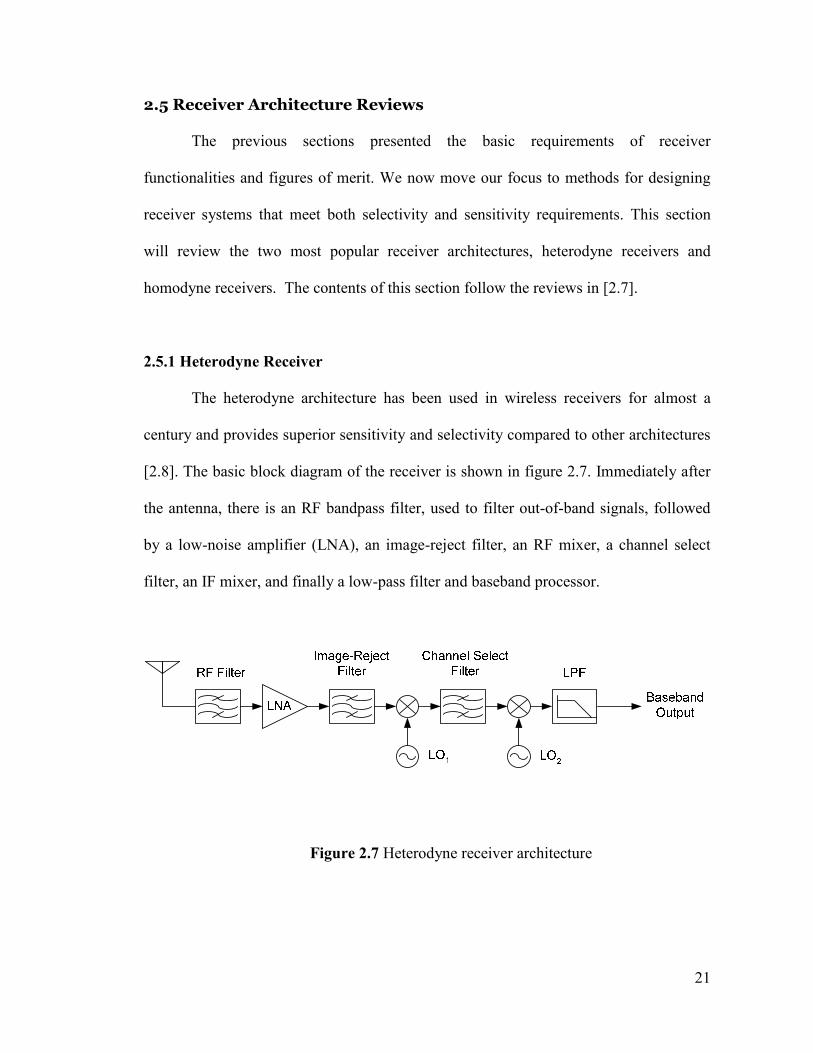
[2.8]. The basic block diagram of the receiver is shown in figure 2.7. Immediately after
the antenna, there is an RF bandpass filter, used to filter out-of-band signals, followed
by a low-noise amplifier (LNA), an image-reject filter, an RF mixer, a channel select
filter, an IF mixer, and finally a low-pass filter and baseband processor.
Figure 2.7 Heterodyne receiver architecture

22
The main concept of this architecture is that the frequency translation process is
divided into two steps. The first is the transition of a signal from radio-frequency (RF)
to the intermediate frequency (IF). The second is the frequency translation from IF to
baseband. The channel filtering takes place at the IF frequency by a bandpass filter with
fixed center frequency at the IF. This means that the channel selection takes place at the
first mixing process by selecting the local oscillator (LO) frequency, such that the RF
signal is shifted down by different amounts to locate the desired channel at the fixed IF.
Performing channel filtering at the fixed IF frequency greatly relaxes the requirements
on the channel-select filter. Channel filtering at the RF frequency would require a
tunable RF filter with prohibitively high quality factor (Q).
The RF bandpass filter is a fixed-frequency filter that attenuates out-of-band
signals. The low-noise amplifier then provides primary gain for the receiver front-end.
As shown in section 2.2, this first block in the receiver chain (besides the bandpass
filter) has significant impact on the overall noise in the system. Thus, the main objective
of the LNA design is to provide large gain with minimal noise. The other constraint in
the LNA design is that its input impedance must match the output impedance of the RF
filter, which is usually 50 Ω.
Since the same frequency components at IF frequencies can be created by RF
signals on both sides of the LO, an undesired image signal will be superimposed on the
desired signal after the first mixing (figure 2.8). This image signal can be comparable in
magnitude to the desired signal, and may obscure all the information if not treated
properly. In this case, an image reject filter is used before the first mixing to attenuate
the image of the desired RF signal.

23
Although the RF bandpass filter suppresses the image signal to some extent, it
will be amplified by the LNA before mixing. This is why the image-reject mixer is
placed immediately before the mixer. This filter also suppresses noise in the image
band.
Figure 2.8 Image problem
The heterodyne architecture provides superior selectivity performance due to the
benefits from including the IF stage. However, it requires many functional blocks in the
system, and many of the blocks are very hard to integrate on-chip. For example, the
image-reject and channel-select filters are difficult to implement on-chip due to the
relatively low quality factor (Q) of the on-chip inductors. The need for additional off-
chip components results in higher passive component costs, chip pin count, and extra
board areas.
2.5.2 Homodyne Receiver
For a homodyne receiver (figure 2.9), the RF signal is downconverted directly to
DC (or near-DC) by matching the LO frequency to the center frequency of the RF

24
passband. In the direct-conversion case, where the signal at RF is converted to baseband
directly, the signal is placed on both sides of the LO frequency, as shown in figure 2.10.
If complex modulation is used, which is more bandwidth-efficient, there will be
garbling due to negative frequency components going to positive frequencies and vice
versa, and an image-rejection mechanism will still be required. However, since the
image is the mirror of the signal itself, the power level of the image is the same as the
level of the desired signal. As a result, the image-rejection requirements can be relaxed
and could be achieved with simple image-reject mixer architectures. In addition, since
the channel filtering is now done at baseband, it is possible to implement it as a high-
order on-chip low-pass filter.
Figure 2.9 Homodyne Receiver
Figure 2.10 Direct-conversion frequency plan

25
Direct-conversion systems, however, do have some serious problems not present
in heterodyne systems. Because the signal is now mixed directly to DC, any DC offset
in the receiver path can corrupt the desired signal or saturate the signal path. The
unwanted DC offsets can be removed by placing an AC coupling capacitor at the mixer
output. However, this may adversely impact the bit-error-rate, since the signal energy at
DC will be removed as well. In high-bandwidth systems such as wireless LANs, the use
of an on-chip AC coupling capacitor might be acceptable without significant penalties
[2.9]. However, in a system with narrower channel bandwidths, the AC coupling
capacitors, if used, are of such a size such that they must be placed off-chip [2.10].
Techniques used to reduce the DC content of the signal through coding or redefinition
of the baseband signal can be used to alleviate this problem. Another approach to
removing the offset is to use the training signal to estimate the existing DC offset. Based
on this estimation, the offset can be removed or omitted from the mixer output [2.11].
However, this method does not address dynamic DC offset or 1/f noise problems.
An alternative technique for addressing the DC offset problem in the direct-
conversion receiver is the use of low-IF architecture [2.12]. In this case, the RF signal is
down-converted to a very low IF, instead of baseband. In this case, the DC offset
problem is relaxed, since the power at DC can be removed by using an on-chip AC
coupling capacitor without significantly affecting the desired signal. However, the
image becomes a larger problem; in this case, the image power is set by the blocking
profile and usually grows stronger as the frequency moves away from the carrier. To
minimize the image rejection requirement, the IF frequency is usually not more than one
or two channels away from the DC, where the blocker levels are still relatively low. All

26
of the image rejection must be performed with a Weaver-like structure or polyphase
filter (see next section) and this strongly depends on the matching between I and Q paths
of the receiver. The other drawback of this architecture is that it requires higher-
bandwidth baseband blocks because the signal is now moved to a higher frequency.
2.5.3 Image-Reject Mixers and Complex Filters
Several systems have been proposed to solve image problems in receivers
without using an off-chip image-reject filter. These systems are called image-rejected
architectures. The most common are Hartley image-reject mixers, Weaver image-reject
mixers complex filters are reviewed in this section. More complete descriptions and
analysis of these architectures can be found in [2.5], [2.13].
2.5.3.1 Hartley Architecture
The Hartley architecture is shown in figure 2.11. Note that the 90° phase-shifter
is a Hilbert transformer with the transfer function:
( ) ( )njjH sgn−=ω (2.27)
The multiplication of the RF signal with the 90° phase-shifted LO followed by
the 90° degree phase-shift inverts the signal on one side of the LO, thus distinguishing
the signal from the image. Adding this to the signal that is downconverted with non-
phase-shifted LO leads to image-rejection. A disadvantage of this architecture is the

27
need for a wideband phase-shifter that provides 90° phase shifts for the entire signal
bandwidth.
Figure 2.11 Hartley Architecture
2.5.3.2 Weaver Architecture
Figurer 2.12 Weaver Architecture
Unlike the Hartley architecture, the Weaver architecture uses two additional
mixers placed after the low-pass filters to perform the phase-shifting instead of using a

28
wideband phase shifter. The RF signal is first downconverted to an intermediate
frequency, then downconverted once again to the “final” IF. After the first down
conversion, one path is multiplied by the sine wave, which is simply the phase-shifted
cosine wave, equivalently downconverting the signal to the output frequency and phase-
shifting it by 90° at the same time. The other path, which is multiplied by the cosine
wave, is downconverted without the phase shift. As in the Hartley architecture,
summing these two paths results in image rejection.
An advantage of using the Weaver architecture is that the wideband phase shifter
is no longer needed. Although the 90° phase shifters for the LO quadrature signals are
still needed, they are narrowband and easier to design.
2.5.3.3 Complex Filters
Besides image-reject mixers, complex filters are important and are widely used
in receiver designs, especially in low-IF architectures [2.14][2.15]. Complex filters use
cross-coupling between the real and imaginary signal paths in order to realize filters
with transfer functions that do not have the conjugate symmetry (in the frequency
domain) of real filters. This implies that their transfer functions have complex
coefficients. The filters can be realized using basic operations, i.e., addition,
multiplication, and delay operations for discrete-time digital filters, or the integrator
operator for continuous-time analog filters. More information on complex mixers is
given in [2.13].

29
2.6 Multi-Band Receivers Using Broadband Front-End
A recent trend in the electronics industry has been to integrate many features,
including multi-band multi-standards compatibility, in a single handheld device. This
has created a need for receivers that are compatible with as many standards as possible.
In this section, we will focus on preliminary architectures and issues in designing
universal radio front-ends. We will begin by discussing the challenges in designing a
broadband receiver. An important issue is that most existing receiver topologies are
designed for a fixed single band, or only a few bands [2.16][2.17]. Next, we will
investigate the possible implementations for a universal radio receiver using
architectures modified from those presented earlier in this chapter. We will compare
topologies in terms of their suitability for integration and multi-band capabilities.
Finally, we will give a performance estimation of a broadband receiver based on the
selected topology.
2.6.1 Possible Front-end Implementations
Unlike conventional narrow-band receivers, universal receiver front-ends must
be able to detect and process signals at different frequency bands. Since the operations
are still narrow-band, one way to implement the receiver is to use a high-Q tunable RF
bandpass filter for frequency band selection, in conjunction with a broadband LNA and
mixer, as shown in figure 2.13. The RF filter is required in order to attenuate any out-of-
band jammers and relax the front-end linearity requirements. For example, the out-of-
band jammers could be as high as 0 dBm for the GSM standard, as shown in figure 2.3.

30
Such a high-Q tunable RF bandpass filter is difficult if not impossible to
implement on a silicon substrate (such as CMOS IC) using current technology [2.5].
However, RF MEMS technology has shown promising results [2.18] and could become
a commercially available option in the future.
LNABaseband
Output
TunableRF Filter
LPF
LO
Figure 2.13 A multi-band multi-mode receiver utilizing a tunable RF bandpass filter
The need for a RF tunable filter can be avoided by implementing the “effective”
tunable RF filter with several high-Q RF bandpass filters placed in parallel, each
covering a frequency band for the intended application. Switches are needed to select
which frequency band to use at a given time, as shown in figure 2.14. Although this
method is acceptable for implementing a few narrow frequency bands, it would become
impractical for generic universal radio or configurable radio, where the receiver must be
able to operate in any band in the required frequency range. Moreover, these switches
need to have low loss and high linearity at high frequency, both of which are not
achievable by CMOS devices.

31
Figure 2.14 A receiver using multiple RF filters and switches
One straightforward solution for the problem of having too many RF bandpass
filters is to not to perform any filtering at all. This leaves the broadband receiver with no
bandpass filters in the front-ends, as shown in figure 2.15. Because there is no bandpass
filtering, any large interfering signals can saturate the signal path or create
intermodulation products that overtake the desired signal. For standards with stringent
out-of-band jammer requirements (GSM, for example), having no out-of-band
attenuation requires an extremely linear receiver front-end, which is very difficult, if not
impossible, to implement in modern CMOS technologies. For some standards such as
wireless LANs, there is no out-of-band blocking requirement for the standard, and the
front-end linearity specifications can be relaxed. However, a high-linearity front-end is
still desirable in this case due to possible jamming situations in real-world applications.
Active research has been done on implementing a receiver that can tolerate large
out-of-band jammers without using filters. For example, an active filtering technique has

32
been proposed for removing an out-of band blocker without using an extra SAW filter in
[2.19]. The circuit employs a feed-forward filter path, and the high-Q characteristic of
the filter is realized by using a translinear loop.
Figure 2.15 A broadband receiver with no RF bandpass filtering
If the receiver is broadband, there will be problems with harmonic distortion and
harmonic mixing, as well as intermodulation distortion problems that also exist in
narrow-band receiver front-ends. For example, if the intended receiving frequency can
be anywhere from 0.5 MHz to 5 GHz, a strong signal at 0.8 GHz will create a third-
order harmonic distortion at 2.4 GHz and will interrupt any desired signals at that
frequency. Likewise, if the desired signal and LO are at 0.8 GHz (narrow channel
bandwidth), a strong signal at 2.4 GHz will mix with LO harmonics locating at 3fLO and
may corrupt the desired signal. Moreover, signals at 0.9 GHz and 2.4 GHz could mix
and create an IM2 that corrupts any desired signals at 1.5 GHz. The problems of
harmonic mixing and wideband harmonic distortion could be alleviated by:
(1) Using harmonic reject mixers that suppress harmonic mixing at near-LO
harmonics such as at 3fLO at 5fLO. An example of such a mixer can be found
in [2.20] and has been used in [2.21].

33
(2) Employing differential circuits in the RF front-end paths to suppress even-
order harmonics or intermodulation.
(3) Limiting the ratio between the highest and lowest frequency of the intended
receiving signals to less than two by using a band-pass filter. In this case,
harmonic distortions of an incoming signal will fall out-of-band and will not
interfere with the intended receiving signal. In addition, any IM2 from two
strong in-band signals will fall out of band since their channel separation will
always be less than the minimum intended receiving frequency. This relaxes
the harmonic mixing problems as well.
Option (3) could be modified for wider frequency band coverage by using
multiple RF bandpass filters, each of which covers a “group” of bands, as shown in
figure 2.16. For example, one might use a filter with 0.8 GHz to 1.5 GHz passband
responses to avoid any mixing between 0.9 GHz and 2.4 GHz signals falling in-band,
and use another filter covering 1.4 GHz to 2.7 GHz to process the signal at 2.4 GHz.
Although this might appear similar to the architecture in figure 2.14, the number of
required RF bandpass filters could be vastly different. For example, to cover the
frequency bands from 0.5 GHz to 5 GHz, the number of filters needed in this topology
would be only 4-6, no matter how many standards exist in the range. (The 4-6 variation
is due to the amount of overlapping and the chosen frequency ratio.) However, this
architecture would likely require out-of-band blocking and linearity requirements
similar to those without any bandpass filter. If needed, multiple broadband LNAs can be
used for signals from multiple frequency groups as well.

34
Figure 2.16 A receiver with multiple “wideband” RF bandpass filter
2.6.2 Broadband Receiver Prototype Example
From the previous section, we can see that the key components are broadband
front-end building blocks regardless of receiver topologies. In this section, we will
examine the basic relationships between the receiver and building block specifications
in a prototype receiver. As a derivative example, the specification requirements of the
prototype will be based on multiple standards presented in Table 1.1. Starting with the
architecture of the receiver prototype, we will then discuss system parameters such as
noise figure, linearity, and dynamic range, as well as block-level specifications.
2.6.2.1 Prototype Receiver Architecture
The conceptual diagram of the receiver can be simplified as shown in figure 2.17.
In the figure, the major receiver building blocks include low-noise amplifiers (LNA),
downconversion mixers, a frequency synthesizer (for LO signal generation), low-pass
filters, variable-gain amplifiers (VGA), and analog-to-digital data converters (A/D).

35 (1) It should be noted that the above conceptual diagram shows only one mixer.
Figure 2.17 Conceptual diagram of the receiver
In this lineup, the LNA is broadband, but it could be designed as one broadband
LNA or several narrow band LNAs in parallel. The I/Q image-rejection mixers
downconvert the incoming signal from RF to IF frequency.(1) The LO signal is supplied
by the frequency synthesizer. The synthesizer needs a voltage-controlled oscillator
(VCO) that has a wide frequency tuning range in order to work with multiple bands and
standards [2.22]. Also, it is necessary to have a channel bandwidth adjustment scheme
that accommodates different channel bandwidths for different standards. Channel
bandwidth adjustments can be implemented using the direct conversion frequency plan
with a tunable low-pass IF filter, or a low-IF architecture with a tunable bandpass IF
filter. The first approach is simpler but may suffer from the problems with DC offset and
1/f noise, especially if the channel bandwidth is low, as in GSM standards [2.3]. The
second approach, on the other hand, does not have low-frequency problems, but the filter
design is more complicated and requires good image rejection. If needed, a low-pass
filter with DC offset cancellation or AC blocking capacitors could also be used in a low-
IF architecture. However, this would result in higher dynamic range requirements for the

36
VGA and the A/D, since the adjacent channel blocker (located near DC at IF) will not be
filtered out.
2.6.2.2 Basic System and Building Block Requirements
As an example, the targeted receiver requirements will be based on multiple
standards shown in Table 1.1, and repeated below in Table 2.1 for important receiver
requirements.
Table 2.1 Receiver requirements for different wireless standards
Range WAN LAN PAN MAN
System GSM/DCS UMTS 802.11a Bluetooth DECT
Frequency 0.9/1.8GHz 2GHz 5GHz 2.4GHz 1.9GHz
Channel spacing 200KHz 5MHz 20MHz 1MHz 1.728MHz
Rx NF 9dB 9dB 7.5dB 23dB 18dB
Rx IIP3 -18dBm -4dBm -20dBm -15dBm -22dBm
Phase noise -141dBc@3M -150dBc@135M -102dBc@1M -105dBc@1M [email protected]
To meet the requirements of all the standards in Table 2.1, the receiver (not just
the front-end) needs to have the following specifications:
Frequency range: 0.9 GHz – 5 GHz
RF Channel bandwidth: 200 kHz – 20 MHz
Noise Figure: 7.5 dB
IIP3 -4 dBm
Phase Noise -141 dBc at 3 MHz

37
Aside from the parameters shown in Table 2.1, receiver designs have many other
requirements. Some examples of these specifications include: IIP2, image rejection, input
compression and desensitization, DC offset corrections, turn-on and turn-around time,
input impedance matching, and filter ripple and group delay requirements. In addition,
several issues that arise specifically with wideband receivers need to be considered, and
will be discussed in section 2.6.1.
In the following analysis, however, we focus only on the requirements for noise
figure, IIP3, signal level plan, and output range, since these performance metrics have the
greatest impact LNA and mixer designs, and these two blocks are the focus of this
dissertation.
The specifications in Table 2.1 are for a receiving path that includes everything
from an antenna to the A/D outputs. In practical applications, any losses due to PCB
traces or passive components at the receiver input will directly increase the overall
system noise figure. Assuming that the total loss between the antenna and the chip pins is
3 dB, the total noise figure at the receiver chip input needs to be 7.5 dB - 3 dB = 4.5 dB.
The system IIP3, on the other hand, could be relaxed by the amount of loss before the
input. In this case, the IIP3 specifications can be reduced to (-4 dBm - 3 dBm) = -7 dBm
at the chip input. However, since the amount of loss varies as frequency changes, and the
exact amount of loss could be higher or lower than 3 dB as a design margin, the IIP3
target should be kept at -4 dBm.
If we allocate 1 dB of noise figure degradation from blocks following the LNA,
the LNA itself needs to have noise figures of 4.5 dB - 1 dB = 3.5 dB or better. For IIP3,
if the IF filter provides sufficient stop-band rejection, any subsequence blocks (such as

38
VGA and A/D) will have minimal impact on the system IIP3 since any interference will
be highly attenuated at the filter output. As a result, the total front-end IIP3 can be
estimated using (2.21) along with the gain and linearity profiles of the LNA, mixers, and
IF filters. An example of an RF front-end building block specification that meets the
noise figure and IIP3 requirements (NF < 4.5 dB, IIP3 > -4 dBm) is given below:
Table 2.2 Example of LNA, mixer, and filter specifications
Blocks Gain (dB) NF (dB) IIP3 (dBm)
LNA 16 3.5 0
Mixer 15 10 15
Filter and subsequence blocks (filter input referred, max gain) 50 20 30
Cascaded (LNA+Mixer) 81 4.1 -3.1
Another important design consideration is the signal level plan, or how the signal
level is adjusted along the receiver path. More specifically, the receiver gain control and
A/D interface need to be chosen so that:
(1) There is enough gain to meet the signal level requirement when the incoming
signal level is low.
(2) The receiver has enough dynamic range to handle significant interference in
the event that the desired signal is weak (near-far problem). Even with channel
filtering, the incoming blockers can be substantially larger than the desired

39
signal at the receiver output. This dictates the receiver linearity requirement,
channel filter out-of-band rejection, and A/D dynamic range.
(3) Finally, in the event that the desired receiving signal is very strong, the
minimum receiver gain (from LNA to VGA) needs to be low enough so that
the output signal level will not be compressed along the signal path (likely at
the VGA output or A/D input). This requirement is different from that in (2)
above because the desired signal will not be attenuated by the filter as in the
previous case.
For example, if a 10-bit A/D with 1Vp-p input full-scale voltage swing is used at
the receiver output, the A/D dynamic range will be approximately 60 dB (around 6 dB
per bit) with 1 mV LSB. The required maximum gain of the receiver can be calculated
from the LSB of the A/D and the required signal level above the A/D quantization noise.
For example, if the system requires the rms signal level to be 30 dB above the A/D LSB,
and the required sensitivity is -100 dBm (-113 dBVrms), the required maximum receiver
gain is then:
( )( ) ( ) dB 83 dBVrms 113- dBVrms 1m20log 30 max =−+=RxGain (2.28)
The required minimum gain of the receiver, on the other hand, can be calculated
from the A/D full-scale range and the largest possible receiving or interfering signal.
Because an unwanted signal will be heavily attenuated by the IF filter, the minimum gain
of the receiver can be determined by the maximum input level of the desired signal and
40
the A/D full-scale range (which is 60 dB above LSB). If the maximum desired input level
is -15 dBm (-28 dBVrms), the required minimum receiver gain is then:
( )( ) ( ) dB 28 dBVrms 28- dBVrms 1m20log 60 min =−+=RxGain (2.29)
Usually, we can attenuate the desired signal at the LNA input, since noise figure
is not a concern in this situation (the signal level is already high, so the SNR degradation
is not a concern). If a large interference is present when the desired signal is low (near-far
situation), the LNA gain must be kept high in order to maintain the low noise figure of
the system, and the filter rejection needs to be large enough to prevent any signal
compression at the receiver output (A/D input). For example, if the interference can be as
high as -20 dBm (-38 dBVrms) while the desired signal is at -100 dBm (-113 dBVrms),
the receiver gain needs to be 83 dB according to (2.28), while the rejection needs to be
high enough to keep the inference level below the A/D range. This can be written as:
( )( ) ( ) ( ) RejectiondB 83dBVrms 38- dBVrms 1m20log 60 −+>+
dB 54 Rejection > (2.30)
Another requirement in this situation is that the blocks preceding the IF filter are
linear enough to handle the -25 dBm interference.

41
2.7 References
[2.1] A. K. Wong, and R. G. Meyer “Blocking and Desensitization in RF Amplifiers,"
IEEE Journal of Solid-State Circuits, Vol. 30, No. 8, August 1995, pp. 944-946.
[2.2] J. C. Rudell, “Frequency translation techniques for high-integration high-
selectivity multi-standard wireless communication systems”, Ph.D. Dissertation,
UC Berkeley, 2000
[2.3] ETSI, “Global System for Mobile Communications”, Digital cellular
telecommunications system (Phase 2+); Radio transmission and reception, GSM
5.05, Version 5.2.0, Copyright 1996.
[2.4] R. G. Meyer, EE242 Lecture Notes, University of California, Berkeley, 2004
[2.5] B. Razavi. RF microelectronics. Prentice-Hall, Upper Saddle River, New Jersey,
1997.
[2.6] A. Behzad, “The implementation of high-speed experimental transceiver module
with an emphasis on CDMA applications” Master Thesis, ERL Memorandum No.
UCB/ERL M95/40, June 1995.
[2.7] B. Limketkai, “The Design and Implementation of A Downconversion Mixer For
a wideband CDMA Receiver”. MS Thesis, UC Berkeley, 1999.
[2.8] T. Lee. The Design of CMOS Radio-Frequency Integrated Circuits. Cambridge
University Press, Cambridge, UK, 1998.
[2.9] D.Yee, et al., “A 2-GHz Low-Power Single-Chip CMOS Receiver for WCDMA
Applications,” Proceedings of ESSCIRC 2000, September 2000, Stockholm,
Sweden.

42
[2.10] C. Hull, et al., “A Direct-Conversion Receiver for 900MHz (ISM Band) Spread-
Spectrum Digital Cordless Telephone,” ISSCC Dig. Tech. Papers, pp. 344-345,
February 1996.
[2.11] J. Cavers and M. Liao, “Adaptive Compensation for Imbalance and Offset Losses
in Direct Conversion Transceivers.” IEEE Transactions on Vehicular Technology,
vol. 42, pp. 581-588, November 1993.
[2.12] M. Steyaert, et al., “A Single-Chip CMOS Transceiver for DCS-1800 Wireless
Communications,” Proceedings of the 1998 ISSCC, pp. 48-49.
[2.13] K. W. Martin, “Complex Signal Processing is not Complex”, IEEE Trans.
Circuits Syst. I, Vol. 51, No. 9, September 2004.
[2.14] J. C. Rudell, J. Ou, T. B. Cho, G. Chien, F. Brainti, J. A. Weldon, and P. R. Gray,
“ A 1.9-GHz Wide-Band IF Double Conversion CMOS Receiver for Cordless
Telephone Applications”, IEEE J. Solid-State Circuits, vol. 32, pp. 2071-2088,
December 1997.
[2.15] J. Crols and M. Steyaert, “Low-IF Topologies for High-Performance Analog
Front Ends of Fully Integrated Receivers”, IEEE Trans. Circuits Syst. II, vol.45,
pp. 269-282, March 1998.
[2.16] M. Zargari, et al., “A Single-Chip Dual-Band Tri-Mode CMOS Transceiver for
IEEE 802.11a/b/g WLAN”, ISSCC Dig. Tech. Papers, pp96-97, February 2004.
[2.17] O. E. Erdogan, et al., “A Single-Chip Quad-Band GSM/GPRS Transceiver in
0.18m Standard CMOS”. ISSCC Dig. Tech. Papers, pp 318-319, February 2005.

43
[2.18] C. Nguyen, “Vibrating RF MEMS for next generation wireless applications,” in
Proc. IEEE 2004 Custom Integrated Circuits Conf., Piscataway, NJ, IEEE Press,
2004, pp. 257-264.
[2.19] H. Darabi, “A Blocker Filtering Technique for SAW-Less Wireless Receivers,”
IEEE J. Solid-State Circuits, vol. 42, no. 12, pp. 2766-2773, December 2007.
[2.20] J. Weldon, et al., “A 1.75-GHz highly integrated narrow-band CMOS transmitter
with harmonic-rejection mixers,” IEEE J. Solid-State Circuits, vol. 36, no. 12, pp.
2003-2015, December 2001.
[2.21] R. Bagheri, A. Mirzaei, S. Chehrazi, M. Heidari, M. Lee, M. Mikhemar, W. Tang,
and A. A. Abidi, “An 800-MHz-6-GHz software-defined wireless receiver in 90-
nm CMOS,” IEEE J. Solid-State Circuits, vol. 41, no. 12, pp. 2860-2876,
December 2006.
[2.22] A. Berny, A. M. Niknejad, R. G. Meyer “A 1.8-GHz LC VCO with 1.3-GHz
Tuning Range and Digital Amplitude Calibration,” IEEE J. Solid-State Circuits,
vol. 40, no. 4, pp. 909-917, April 2005.

44
3
CMOS LNA Fundamentals
3.1 Introduction
In a receiver, the low-noise amplifier (LNA) serves as the first amplification
block along the receiving path. As explained in chapter 2, it is one of the most critical
building blocks of the receiver, since its performance greatly affects both the sensitivity
and selectivity of the system. In this chapter, we will review the basic properties of a
CMOS LNA. Starting with a discussion of noise sources in CMOS transistors in section
3.2, in section 3.3 we will proceed through a classic two-port noise theory. Finally, we
will present a review of input matching and low-noise amplifier topologies.
3.2 Noise Sources in MOS Transistors
Before initiating an analysis of how to design a low-noise amplifier, we must
identify and understand the origins of noise. This section provides insights into the most
important noise sources in MOS transistors, such as drain current noise, induced gate
noise, and flicker noise.

45
3.2.1 Drain Current Noise
Since the channel material in MOS transistors is resistive, it exhibits thermal
noise. This noise source can be represented by a current noise generator connecting from
drain to source in the small signal model, as shown in figure 3.1, and is called “drain
current noise.” The expression for this noise is given by [3.3]:
fgkTi dnd ∆= 02 4 γ (3.1)
where gd0 is the drain to source conductance at zero Vds. The parameter γ has a value of
unity at zero Vds and moves toward 2/3 in saturation for long-channel devices. In the
short-channel device, however, the value of γ can be considerably larger (typically 1.4-2)
due to velocity saturation in short-channel devices [3.4].
2ndi2
ngi
Figure 3.1 Drain current and gate noise models
3.2.2 Induced Gate Noise
The other consequence from the thermal agitation of channel charge, besides
drain current noise, is induced gate noise [3.5]. The fluctuating channel potential couples

46
capacitively into the gate terminal, leading to a noisy gate current. This noise is negligible
at low frequencies because the coupling effect is small. However, it can be problematic at
radio or microwave frequencies. This noise is modeled as a current noise generator
connecting from gate to source in the small signal model (see figure 3.1), and may be
expressed as [3.3]:
fgkTi gng ∆= δ42 (3.2)
where the parameter gg is:
0
22
5 d
gsg g
Cg
ω= (3.3)
The parameter δ is a gate noise coefficient and equals 4/3 for long-channel
devices [3.3], which is twice as large as γ. For short channel devices, however, this value
is still not accurately known. A reasonable approximation is that δ should continue to be
about twice as large as γ. Since γ is around 1.4-2 for the short-channel device, δ should be
around 3-4 [3.5].
As mentioned earlier, the gate noise is related to the drain noise. In fact, it is
partially correlated to the drain noise with a correlation coefficient c, as stated in equation
3.5 below.
22
*
dng
dng
ii
iic = (3.4)

47
The value for c is given in [3.2] as 0.395j for long-channel devices. Since the
coupling between the gate noise and drain noise is through the gate capacitance, the
correlation coefficient is purely capacitive.
One drawback of the induced gate-noise expressions in (3.2) and (3.3) is that the
noise model is frequency dependent. For designers who prefer to analyze circuits using
only noise source models that are frequency independent, it is possible to modify the gate
noise model to a form with a noise voltage source that has a flat spectrum density. To
derive this alternative model, we must first transform the parallel RC network represented
by gg and Cgs into an equivalent series RC network as shown in figure 3.2. If the network
has a reasonably high Q, the capacitance stays approximately constant during the
transformation. The parallel conductance gg becomes a series resistance whose value is:
022 5
111
11
dggg gQgQg
r =≈+
= (3.5)
If we equate the short-circuit elements of the original network and the
transformed version with the assumption of high Q, the equivalent series noise voltage
source is then found to be [3.5]:
=
=∆= 22
222 14C
igr
ifrkTv ngg
gnggng ω
δ (3.6)
which has a constant spectral density. Finally, using (3.6) and (3.4), we can find the
correlation coefficient between the voltage noise to drain current noise as:

48
c
Cii
Cii
iv
ivc
dng
dng
dg
dgv =
==
222222 1
1**
ω
ω (3.7)
which is the same as the correlation coefficient provided by (3.4)
2ngv
2ngi
Figure 3.2 MOS input RC network model transformation
3.2.3 Flicker Noise
The other important noise source in MOS transistors is flicker noise. The origin of
this noise varies, but it is mainly attributed to traps associated with contamination and
crystal defects. Since MOS transistors conduct current near the surface of the silicon,
where traps created by defects and impurities are most plentiful, their flicker noise
components can be large. These traps capture and release carriers in random fashion, and
the trapping times are distributed in a way that leads to a 1/f noise spectrum.
Flicker noise can be modeled as a current noise generator connecting from drain
to source in the small signal model and can be expressed by [3.5]:

49
fWLC
gf
Ki
ox
mfnf ∆= 2
22 (3.8)
where Kf is a constant that depends on the technology process. Cox is the gate oxide
capacitance per unit area. Note that the flicker noise is inversely proportional to the area
of the gate (WL) because the larger gate capacitance smoothens the fluctuation in channel
charges. Also, it is worth mentioning that flicker noise is always associated with a flow
of direct currents. If there is no direct current flowing in the device, this noise should be
minimal [3.6].
3.2.4 Other Noise Sources
The distributed gate resistance of the CMOS transistor also contributes to the
noise in low-noise amplifiers. This noise source is usually modeled as a series resistance
at the gate and the noise power is given by:
gg kTRf
v4
2
=∆
(3.9)
Ln
WRR sq
g 23= (3.10)
where Rg is the gate resistance, Rsq is the sheet resistance of polysilicon, and n is the
number of fingers. The factor 3 comes from the distributed nature of the gate resistance
assuming that each finger is only contacted at one end. If both ends are contacted, the

50
factor became 12. Increasing the number of fingers for a given overall transistor width
decreases the transistor width per finger, and reduces gate resistance noise.
Another noise source mentioned in [3.7] is from resistance due to the lightly doped
drain diffusion regions. Because no distinction is made between the source and drain,
this resistance is also present at the source, and cannot be mitigated by proper layout.
This resistance is given in equation by:
W
RR LDSdrainsource =, (3.11)
where RLDS is the resistance per unit transistor width.
3.3 Two-Port Noise Theory
In this section, we will look at noise from a macroscopic point of view in a two-
port network. Using the system model greatly simplifies the noise problems, as will be
shown later in this chapter.
Starting with the model in figure 3.3a, the linear noisy two-port network is driven
by a source with admittance Ys. If we are interested in only the input-output behavior, it is
not necessary to keep track of all the internal nodes and noise sources of the circuits. In
this case, the noisy two-port network can be replaced by a noiseless two-port network
with external current and voltage noise generators at the input as shown in figure 3.3b.

51
(a)
2ni
2nv
(b)
Figure 3.3 (a) Noisy two-ports driven by noise source, (b) equivalent noise model
Recall from chapter 2 that the noise factor is defined as:
sourceinpout todue noiseoutput power noiseoutput total
≡F (3.12)
All the noise sources are now input-referred, as in figure 3.3b, and the output
power contribution from each term is proportional to its short-circuit current at the input.
As a result, we can now derive the noise factor by calculating the total short-circuit mean-
square input noise current, and divide that total by the short-circuit mean-square noise
current generated from the input source. The expression then becomes:

52
2
2222
s
nsns
i
vYiiF
++= (3.13)
In the equation above, we have assumed that the noise from the source and the
equivalent noise generators are not correlated. However, there is a correlation between
the current noise generator and the voltage noise generator. We can write in as:
ucn iii += (3.14)
Where ic is the part of in that is correlated with vn, and iu is the part of in that is
uncorrelated with in. Since ic is correlated with vn, it can be written as:
ncc vYi = (3.15)
The constant Yc is known as the correlation admittance [3.5].
Putting (3.14) and (3.15) into the equation (3.13), we get a modified expression
for the noise factor:
( )2
222
2
2222
1s
nscu
s
nscus
i
vYYi
i
vYYiiF
+++=
+++= (3.16)
The expression above contains three independent noise sources. We can then define:
fkTvR n
n ∆=
4
2
(3.17)
fkTiG u
u ∆=
4
2
(3.18)
fkTiG s
s ∆=
4
2
(3.19)

53
Using equations (3.16)-(3.19), we can then write the noise factor in terms of noise
admittances and impedances as:
( ) ( )[ ]s
nscscu
s
nscu
GRBBGGG
GRYYG
F222
11++++
+=++
+= (3.20)
At this point, the optimal admittance can be found by taking the first derivatives
of the equation above with respect to the source conductance and source susceptance and
turning it into zero. This yields:
optcs BBB =−= (3.21)
optcn
us GG
RG
G =+= 2 (3.22)
Substituting (3.21) and (3.22) into (3.20) gives the following result for the
minimum noise figure:
( )coptn GGRF ++= 21min (3.23)
Using equation 3.21, we get the general expression for noise figure:
( ) ( )[ ]22min optsopts
s
n BBGGGR
FF −+−+= (3.24)
From equation 3.24, it can be seen that the contours of constant noise factor (and
noise figure) are circles centered about (Gopt, Bopt) in the admittance plane.

54
3.4 Impedance Matching in LNA Designs
Impedance matching is important in an LNA design because the system
performance is often strongly affected by the quality of the termination [3.7]. For
instance, the frequency response of the antenna filter that precedes the LNA will deviate
from its normal operation if there are reflections from the LNA back to the filter.
Furthermore, undesirable reflections from the LNA back to the antenna must also be
avoided. An impedance is matched when ZS = ZL as in figure 3.4.
Figure 3.4 Condition for an impedance match
There is a subtle difference between impedance matching and power matching.
As stated in the previous paragraph, the condition for impedance matching occurs when
the load impedance is equal to the characteristic impedance. However, the condition for
power matching occurs when the load impedance is the complex conjugate of the
characteristic impedance. When the impedances are real, the conditions for power
matching and impedance matching are the same.

55
3.5 LNA Input Matching Topologies
As mentioned in the previous section, impedance matching is very important in
LNA designs. In most cases, the source impedance of the LNA is 50 Ω in a wireless
system. Since the input impedance of the MOS transistor is almost purely capacitive,
providing a good match to the source without degrading noise performance is a
challenge. In this section, we will investigate a number of circuit topologies that can be
used for the tasks and discuss their properties.
3.5.1 Resistive Termination
This is the most straightforward approach to achieve broadband 50 Ω matching at
the input, as shown in figure 3.5. The 50-Ω resistor (R1) is placed across the input
terminal of the LNA thus providing a broadband input matching if R1 equals RS.
RL
M1VS
R1
RS
Rin
Figure 3.5 Resistive termination matching

56
The matching bandwidth of this matching topology is determined by the input
capacitance of the transistor M1 and is given by:
( )SgdB RRC
f//2
1
13 π
=− (3.25)
where Cg is the equivalent capacitance looking into the gate of M1. For deep-submicron
CMOS technology, Cg could be in the range of 1-2 pF for devices with moderate
transconductance. This leads to several gigahertz of bandwidth in a 50-Ω system.
However, the resistor R1 adds its own thermal noise to the circuit and attenuates
the incoming signal by a factor of two before it hits the gate of the transistor. These two
effects result in a high noise factor of the circuit, hence the method is not practical in low-
noise applications. Ignoring all the noises from the transistors and subsequence circuits,
the lower bound of the noise factor is 2 in an ideal match condition.
3.5.2 Shunt-Series Feedback
Another method used to obtain good input matching is the shunt-series feedback
amplifier, as shown in figure 3.6. Unlike the resistive termination case, it does not
attenuate the signal by a noisy attenuator before reaching the gate of the amplifying
device, so the noise figure can be much better. However, the feedback resistor continues
to generate thermal noise of its own and could contribute significantly to the overall
output noise.

57
Figure 3.6 Shunt-series feedback matching
If R1=0, the input resistance of the amplifier shown above is (detailed analysis
will be given in chapter 7):
Lm
FLin Rg
RRR+
+=
1 (3.26)
Since Rin is determined by RL, RF, and gm, it is possible to design the matching
stage with M1 having high gm and low input referred noise. This input match design
flexibility, in addition to its simplicity and compactness, makes a shunt-feedback LNA
topology an attractive choice for multi-band LNA designs. Chapter 7 provides a detailed
analysis and a design example of a low-power differential shunt resistive LNA as part of
a wideband receiver front-end.
Several works on broadband CMOS LNAs have been published using resistive
shunt-feedback architecture or its variations [3.8][3.9][3.10]. For example, in [3.8], a
resistive feedback LNA with 3-dB bandwidth higher than 8 GHz and noise figure below

58
3 dB is reported. The LNA, which is single-ended, has been implemented in 90-nm
CMOS technology with active area of 0.025 µm2, and consumes 42 mW from a 2.7 V
supply.
3.5.3 Common-Gate Input
Another method for realizing resistive input matching is to use a common-gate
configuration. As shown in figure 3.7, the source terminal is used as an input terminal. As
the figure also shows, the source terminal is used as an input terminal. Since the
impedance looking into the source of a common gate amplifier is 1/gm, it can be set by
proper device sizing and by adjusting the bias current of the circuit. This creates a
drawback of this configuration, in that gm is fixed once the source resistance is known.
Figure 3.7 Common-gate input matching
Since the input resistance is the reciprocal of transistor gm and the dominant
capacitor at the input terminal is the device Cgs, we can expect that the matching
bandwidth is close to the transition frequency (ft) of the device.

59
Neglecting gate and flicker noises and assuming a perfect match, we can express
the lower bound of the noise figure for the amplifier that uses this matching technique as:
0
1d
m
ggF γ
+≥ (3.27)
The numerical value for the lower bound expressed above is about 2.2dB for
long-channel devices and 4.8dB for short-channel devices [3.5].
The Rin=1/gm restriction can be avoided by applying a modified version of the
input signal at the gate of M1 in order to manipulate the effective gm of the device, as
shown in figure 3.8.
Figure 3.8 Common-gate input matching with gain boosting
In this case, the effective transconductance of M1 can be described by
( )VmMm AgG −= 11, (3.28)

60
If Av is negative, the effective transconductance increases by a factor of 1+|AV|,
and the input resistance decreases by the same factor. For low-power applications, the
method can be used to reduce the required gm and bias current for a given input
impedance requirement. In addition, the gain stage with Av of -1 can be easily realized in
a differential input structure when an inverted version of the input signal is available on
the other side of the input. This technique has been used in [3.11] in conjunction with a
complementary PMOS-NMOS current reuse architecture to achieve four times higher gm
without additional device bias currents.
The signal applied at the gate M1 (as in figure 3.8) can also be implemented by
using a feedback network that feeds back the signal from the LNA output. The work
presented in [3.12] uses a negative feedback around a common base stage of the BJT
input device to reduce the noise, and correlates the input impedance to the output load
using a capacitive divider as a feedback network. Since the feedback is capacitive, the
architecture allows easy reconfigurability of the amplifier with very little noise
degradation. However, this architecture requires a device with high current gain and low
output capacitances in order to achieve sufficient loop gain; thus it becomes less
attractive when CMOS is the process technology to be used instead of BiCMOS, where
fast BJT devices with low collector capacitances are available.
Another way to use a feedback network to change the input impedance of a
common-gate stage is shown in figure 3.9 [3.13]. In this circuit, a positive current
feedback network via M2 is used to add an extra degree of freedom between the value of
Rs and gm1. The input impedance in this circuit topology is given by [3.13].

61
( )Lmmin Rgg
R21 1
1−
= (3.29)
Figure 3.9 Common-gate input matching LNA with positive feedback
If gm2RL is close to but lower than unity, the value of gm1 can be chosen to be
much higher than 1/RS. This allows the use of high-gm input devices that have lower input
referred noise, resulting in an achievable noise figure close to that of the inductively
degenerated amplifier [3.14].
Since the feedback is positive, careful design is needed to ensure that the
amplifier is stable over all frequency ranges. This could be especially challenging when
process variations are taken into account and the gm2RL product is close to unity (to allow
higher gm1).

62
3.5.4 Noise-Canceling LNA Architecture
As discussed in section 3.5.3, the transconductance value of the input device in
the common-gate architecture is required to be 1/RS unless extra circuitry is added to alter
the effective transconductance of the device. This is also the case in a shunt-feedback
amplifier when gmRL >> 1 and RF << RL. In both cases, this requirement results in high
noise contributions from the input transistor and a high noise figure of the circuit. This
noise contribution from the input devices, however, could be suppressed by using noise-
cancelling techniques [3.15][3.16][3.17].
Figure 3.10 shows a version of a non-canceling low-noise amplifier as reported in
[3.15]. It consists of the input matching part and the noise canceling circuitry path. First,
let us consider the desired signal (VS) coming from the voltage source. Due to the
inverting nature of the shunt feedback amplifier, the scaled version of the desired signal
at node X will have opposite polarity compared to the scaled version of the signal at node
Y. In contrast, the noise voltages at node Y and X generated by the drain current noise of
M1 have the same phase. If a noiseless stage with the gain of -Av is added to amplify the
signal at node X, the amplified output signal of this gain stage, which is at node Z, will
have the same polarity as the signal at node Y. The noise voltage due to the drain current
noise of M1, however, will appear at node Z with the phase opposite to the noise voltage
at node Y. By adding together the signal and noise at nodes Y and Z, the desired signal
will be added constructively while the noise from nodes Y and Z will cancel, resulting in
a signal to “M1 noise” ratio that is much higher than at node Y.

63
M1VS
RS
Rin+
-Av
In,M1 current noise path
RF
Desired Signal
Noise from M1 (drain current noise)
X
Y
Z
Out
Figure 3.10 Shunt-feedback LNA input matching with noise-canceling
Due to the noise-canceling mechanism, the transconductance of M1 could be
chosen almost entirely by input matching considerations since its noise contributions can
be significantly reduced. However, noise contributions from the noise-canceling path (-Av
path) are not canceled out, and the input referred-noise of this path must be kept low.
Another low-noise amplifier with noise-canceling input match is shown in figure
3.11 [3.16]. This circuit consists of common-gate (M1) and common-source stages (M2)
connecting at the input node. If the parasitic capacitance at the gate of M2 is relatively
small, the input impedance of this amplifier will be determined by the common-gate stage
(M1), and can be set to Rs by setting the gm of M1. If we take the output differentially at
the drain of M3 and M4, the voltage gain through the path of M1 and M2 will be
constructive (that is, the amplified signal at the drain of M3 will be out-of-phase
compared to the amplified signal at the drain of M4).

64
Figure 3.11 Common-gate common-source LNA input matching with noise-canceling
In contrast, the output noise due to the drain noise of M1 is in the same phase at
the drain of M3 and the drain of M4. When the output is taken differentially, these two
particular noise voltages will cancel each other out. If the values of R2, R3, gm1 and gm2
are chosen carefully, the drain noise from M1 can be substantially reduced. Since the
dominant noise source in a traditional common-gate amplifier is the drain current noise of
M1, the input-referred noise of M2 could be made low by increasing M2’s gm without
input matching constraints, and very low noise figure could be achieved.

65
A common-gate common-source thermal noise-cancelling architecture similar to
the one in figure 3.12 could also be combined with non-linearity canceling architecture
(the concepts of non-linearity cancellation will be discussed in chapter 7), as reported in
[3.17]. In this work, the input is a complementary common-gate stage that incorporates
both PMOS and NMOS to increase current efficiency. Bias voltages on the input devices,
both common-gate and common-source stages, can be set to obtain both noise and
nonlinearity cancellation simultaneously. Lastly, the output is taken single-ended by
adding an extra common-source stage at the common-gate stage output and combining its
output current to the current coming from the main common-source stage.
3.5.5 Inductive Source Degeneration
Unlike the previously discussed techniques, this matching topology provides a
perfect match without adding any noise to the system or creating any restrictions on the
device gm. It uses an inductor as a source degeneration device and has another inductor
connecting to the gate as shown in figure 3.12.
Lg
Ls
M1
Zin iout
Figure 3.12 Inductive source degeneration matching

66
Using small signal analysis, and neglecting the gate resistance as well as the Cgd
of M1, the impedance looking through the gate inductor can be expressed as:
sTgs
sgin LCj
LLjZ ωω
ω +++=1)( (3.30)
gs
mT C
g=ω (3.30)
At the resonance frequency where the inductor impedance and the capacitor
impedance are canceled out, the input impedance is the last term in the equation (3.30).
The tuned impedance is then given by:
( ) sTeqin LRZ ωω ==0 (3.31)
( ) gssg CLL +=
10ω (3.32)
Since all the inductors are reactive, they do not add any noise into the circuit. In fact,
the LC resonating mechanism improves noise and gain performance of the amplifier
due to voltage gain from the resonance mechanism. Starting from the equivalent
model of the input matching (figure 3.13), the quality factor of the circuit is given by:
eq
gs
RC
Qω
= (3.32)

67
At the resonance frequency, the voltage amplitude across the Cgs is Q times the
voltage across the input terminal from the source, given a matched condition. This
effectively increases the transconductance of the input transistor by a factor of Q.
mm QgG = (3.33)
Lg + Ls
Req
Zin
VSRS
Cgs
Figure 3.13 An equivalent circuit for the inductively degenerated input match
In typical narrow-band matching, this factor is usually around 2-5. Assuming that
the matching network is lossless, this effect helps reduce the input-referred added noise
by a factor of Q and increases the voltage gain of the circuit by the same factor. As a
result, this topology is preferred in most narrow-band applications.
One major limitation of this topology is that the matching is narrow-band. As can
be seen from equation 3.28, the input impedance is a series RLC network with finite Q.
Since most wireless receivers are narrow-band, this is usually not a major concern.
However, for broadband or multi-band receivers, achieving a very wide matching
bandwidth requires the network to have very low Q, resulting in low gain and a poor
noise figure of the LNA.

68
If the LNA is implemented in a deep-submicron CMOS process, Cgs of M1 can be
very small such that Lg could be too large to be implemented on-chip. To solve this
problem, an extra degree of freedom could be added by placing an extra capacitor across
the gate-source terminal of M1 [3.18]. This extra capacitor is used to increase the
effective capacitance into the gate of M1, resulting in a smaller required value of Lg for
the same frequency of application. Unlike increasing the effective Cgs by directly
increasing the size of M1, this extra capacitor neither changes the amount of the intrinsic
gate induced noise (3.2) nor increases Cgd and Cdb of M1.
3.6 References
[3.1] R. Lu, “CMOS Low Noise Amplifier Design for Wireless Sensor Networks,”
Master’s Thesis, UC Berkeley, 2003.
[3.2] Y. Tsividis. Operation and Modeling of the MOS transistor. McGraw-Hill,
Boston, 1998.
[3.3] A. Van Der Ziel. Noise in Solid-State Devices and Circuits. New York: Wiley,
1986.
[3.4] A. J. Scholten, et al., “Accurate Thermal Noise Model for Deep-Submicron
CMOS,” IEEE International Electron Devices Meeting, IEDM Technical Digest,
pp. 155-158, Dec.1999.
[3.5] T. Lee. The Design of CMOS Radio-Frequency Integrated Circuits. Cambridge
University Press, Cambridge, UK, 1998.
[3.6] P. R. Gray, R.G. Meyer, P. J. Hurst, and S. H. Lewis, Analysis and Design of
Analog Integrated Circuits, Fourth Edition, Wiley, New York, 2001.

69
[3.7] J. Janssens and M. Steyaert. CMOS Cellular Receiver Front-Ends. Kluwer, The
Netherlands, 2002.
[3.8] J. Zhan and S. Taylor, “A 5-GHz Resistive Feedback CMOS LNA for Low-Cost
Multi-Standard Applications,” in IEEE Int. Solid-State Circuits Conf. Dig. Tech.
Papers, San Francisco, CA, Feb. 2006, pp. 721-730.
[3.9] Bevilacqua, M. Camponeschi, M. Tiebout, A. Gerosa, and A. Neviani, “Design of
broadband inductorless LNAs in ultra-scaled CMOS technologies,” in IEEE
International Symposium on Circuits and Systems, Seattle, CA, May 2008, pp.
1300-1303.
[3.10] B. Perumana, J. Zhan, S. Taylor, B. Carlton, and J. Laskar, “Resistive Feedback
Low-Noise Amplifiers for Multiband Applications,” IEEE Transactions on
Microwave Theory and Techniques,” vol. 56, no. 5, May 2008, pp 1218-1225.
[3.11] S. Wang, A. Niknejad, and B. Brodersen, “Design of a Sub-mW 960 MHz UWB
CMOS LNA,” IEEE J. Solid-State Circuits, vol. 41, no. 11, Apr. 2006, pp. 2449-
2456.
[3.12] A. Liscidini, M. Brandolini, D. Sanzogni, and R. Castello, “A 0.13 µm CMOS
Front-End, for DCS1800/UMTS/802.11b-g With Multiband Positive Feedback
Low-Noise Amplifier,” IEEE J. Solid-State Circuits, vol. 41, no. 4, Apr. 2006,
pp. 981-989.
[3.13] P. Rossi, A. Liscidini, M. Brandolini, and F. Svelto, “A Variable Gain RF Front-
End, Based on Voltage-Voltage Feedback LNA, for Multi-Standard
Applications,” IEEE J. Solid-State Circuits, vol. 40, no. 3, Mar. 2005, pp. 690-
697.

70
[3.14] A. Liscidini, M. Brandolini, P. Rossi, F. Torrisi, and F. Svelto, “Design
methodology of feedback-LNAs for GHz applications,” in Proc. Bipolar/BiCMOS
Circuits and Technology Meeting (BCTM), Sep. 2004, pp.253-256.
[3.15] F. Bruccoleri, E. Klumperink, and B. Nauta, “Wide-Band CMOS Low-Noise
Amplifier Exploiting Thermal Noise Canceling,” IEEE J. Solid-State Circuits,
vol. 39, no. 2, Feb. 2004, pp. 275-282.
[3.16] S. Chehrazi, A. Mirzaei, R. Bagheri, and A. Abidi, “A 6.5 GHz wideband CMOS
low noise amplifier for multi-band use,” in Proc. IEEE Custom Integrated
Circuits Conf., Sep. 2005, pp. 801–804.
[3.17] W. Chen, G. Liu, Z. Boos, and A. Niknejad, “A Highly Linear Broadband CMOS
LNA Employing Noise and Distortion Cancellation,” IEEE J. Solid-State
Circuits, vol. 43, no. 5, May 2008, pp. 1164-1175.
[3.18] T. Nguyen, C. Kim, G. Ihm, M. Yang, and S. Lee, “CMOS Low Noise Amplifier
Design Optimization Techniques,” IEEE Trans. on Microwave Theory and
Techniques, vol. 52, no. 5, May 2004, pp. 1433-1442.

71
4
Broadband CMOS LNA
Analysis and Design
4.1 Introduction
As discussed in chapter 2, a broadband low-noise amplifier (LNA) is an essential
building block for all of the mentioned multi-band receiver front-end architectures. This
chapter will review the design of such an LNA using a multi-section input matching
network as presented in [4.1]. Starting with topology reviews, we will proceed through
design considerations and implementation. Finally, experimental results will be
presented.
4.2 Multi-Section Input Matching
Most LNAs now in use for integrated wireless receivers are narrow-band, and
each is optimized for only one frequency band of operation. The design methodology for
these LNAs is straightforward, and most are designed using an inductively degenerated
topology that delivers both noise and power match at the same time [4.2].
To broaden the bandwidth of the input matching and gain, we could use the multi-
section input matching topology, which is a modified version of the inductively
degenerated LNA [4.1][4.3][4.4].

72
Figure 4.1 shows a generalized schematic of the broadband input matching
topology, where N is the number of input stages. Please note that the external Cp is added
between the gate and source of M1 in order to increase the degree of freedom in the
design.
Lg
Ls
M1
Zin iout
L1 C1 L3 C3 LN CN
L2 C2
Cp
Figure 4.1 A generalized schematic of the multi-stage input matching topology
Using (3.24), and ignoring the effect of Cgd, the input impedance of the LNA
excluding Ln’s and Cn’s is given by:
Tt
gt
sm
tgin R
sCsL
CLg
sCsLZ ++=++=
11 (4.1)
where
gspt CCC += (4.2)
Combining Zin with Ln’s and Cn’s, we get the equivalent circuit for the input
impedance, as shown in figure 4.2. The impedance Zin and the entire Ln’s and Cn’s form a
bandpass filter with the termination resistor RT. If we look at the inductive degeneration

73
topology as a first-order filter, the addition of Ln’s and Cn’s effectively increases the order
of the filter beyond first-order. From filter theory [4.5], it is easier to get high bandwidth
from a higher-order filter than from a lower-order filter, given the same or comparable
component values and quality factor. This makes wideband matching feasible for multi-
stage input matching.
L1 C1L3 C3 LN CN
L2 C2 Lg + Ls
RT
Zin
Ct
Z’in
Figure 4.2 Equivalent input impedance of the multi-section input matching
4.2.1 Input Matching
In order to get an input match, the real part of the input impedance (Z’in) must be
equal or close to the source impedance RS. If RT = ωTLs = RS and the filter has 0 dB gain
with a ripple of ρr (note that ρr is defined so that 0 dB ripple means ρr =1), the input
reflection coefficient can be related to the ripple by [4.3]:

74
2
2 11r
in ρ−=Γ (4.2)
In the matched condition, the power delivered into the load RT must be the same
as the amount power delivered to the load as if Zin is simply a resistor Rin = RS, which we
call the available power. If the power delivered to the load is less than this available
power, the input matching is then not perfected and it is considered that a portion of the
available power is reflected. The reflection coefficient is then simply the ratio between
the reflected power and the power available to the load, as expressed in (4.2).
For a numerical example, we need to have 0.953 ≤ ρr (about 0.46 dB) for an input
matching of –10 dB or better. This translates to less than 0.46 dB gain variation in the
passband. The plot between passband ripple and the reflection coefficient (both in dB) is
shown in figure 4.3. Once the input matching requirement is chosen, the reactive element
values for any given bandwidth and matching specifications can be obtained by using a
well-established LC filter design methodology as presented in [4.5] and [4.6].

75
-30
-25
-20
-15
-10
-5
00 0.5 1 1.5 2 2.5 3
Passband Ripple (dB)
Inpu
t S11
(dB
)
Figure 4.3 Relationship between passband ripple and reflection coefficient (S11)
4.2.2 Effective Transconductance
The effective gm depends on the device gm and the voltage transfer function from
the input terminal to the vgs at the device terminal. Assuming the transfer function of the
filter is ( )ωjW , the current flowing into the gate of M1 is then given by [4.3]:
( )ωjWRvi
T
ininM =,1
(4.3)
where vin is the terminal voltage as shown in figure 4.2. In the passband, ( )ωjW is
approximately unity and the current is simply the terminal voltage divided by RT.
However, ( )ωjW becomes very small out-of-band, and in this case the current transfer

76
function is minimal. The vgs of M1 can be found directly by multiplying the gate current
to the impedance from Cgs:
( )tT
in
t
inMgs Cj
jWRv
Cji
vω
ωω
== ,1 (4.4)
Using (4.4), the effective transconductance is:
( ) ( )tT
m
in
gsmm CRj
jWgvv
gjGω
ωω == (4.5)
If only the magnitude of Gm is concerned, (4.5) can be simplified to:
( ) ( )ωω jWQgjG mm = (4.6)
The expressions in equations 4.5 and 4.6 are generalizations of (3.24) in the
previous chapter. As shown above, the effective Gm of the circuit depends strongly on the
Q of the matching network. For an on-chip implementation, this value is limited by either
the practical values of the inductors or parasitic capacitances on the input transistor.
4.2.3 Noise Analysis
There are several major sources of noise for a multi-section input matching LAN.
The first is loss at the input-matching network due to finite Q of the passive components,
mainly from the input inductors. The other noise sources are the thermal drain and gate
current noises of the input device (M1 in figure 4.1). The optimal device size based on a
given bias current for a narrow-band case is given in [4.2].

77
To see the effect of noise from the transistor in a wideband-matching case, we
will follow the analysis in [4.3]. The input transistor with the degeneration inductor is
shown in figure 4.4a along with its gate and drain current noises, and the noise sources
can be replaced by input referred voltage and current noise sources given by:
ndm
tngn i
gCj
iiω
+= (4.7)
( ) nsm
id
m
ndstngsn iLj
gi
gi
LCiLjv ωωω +=−+= 21 (4.8)
where ind and ing are the drain current noise and the gate current noise, respectively. The
spectrum densities of these two current noises were discussed in the previous chapter and
given as follows:
fgkTi dnd ∆= 02 4 γ (4.9)
fgC
kTid
gsng ∆=
0
222
54
ωδ (4.10)

78
(a) (b)
Figure 4.4 Drain and gate current noise models
These two noises are correlated with a correlation coefficient of approximately
j0.4. This means that the correlation admittance has only the imaginary part and is given
by [4.3]:
ts
tccc
n
nc
CLc
cCj
jBjBGvi
Y2
222211
ωχαρραχ
ραχω
−++
+==+== (4.11)
where tgs CC=ρ , ( )γδχ 5/= , and c is the correlation coefficient between ing and ind.
The parameter 0dm gg=α accounts for short-channel effects due to velocity saturation
and decreasing mobility [4.1][4.5].

79
The optimal source admittance is then given by [4.2]:
( )2
2222
1
21
c
cCRG
GRG
G t
n
uc
n
uopt
−
++==+=
ραχ
χαρραχω (4.12)
2222
211
χαρραχραχ
ω
ω
++
+−
=−=
cc
CL
CBB
ts
tcopt (4.13)
Equation (4.13) shows that the optimal admittance (or impedance) is
approximately the same as the one that resonates with the series combination of Ct and Ls.
This means that a nearly minimum noise figure can be obtained over the wide bandwidth
by using the multi-section matching network, and the corresponding noise factor is given
by:
( )αγω
smn
s
su RgP
RR
RGF +=++≈ 111 (4.14)
where
( ) ( ) ( )222222222
2222
2121
1χαρραχω
χαρραχχαρ
ω +++++
−= cRC
cc
P st (4.15)
As seen from equations (4.14) and (4.15), the noise figure depends on frequency,
device gm, Ct, and other process parameters. For a given bias current, there is an optimal
device size to obtain the minimum noise figure for single frequency.

80
As mentioned previously, there are other sources of noise such as loss at the
input-matching network, physical gate resistance, and substrate resistance. All of these
noise sources must be considered together when designing the circuit. The total noise
figure is then expected to be worse than that given in the equation (4.14).
4.3 0.8-2.4 GHz Broadband LNA Design
Having discussed the matching topology, we now turn to the LNA circuit
implementation. The simplified schematic of the LNA is shown in figure 4.5. It consists
of the main (first) stage and the buffer (second) stage for output matching purposes. Note
that the second stage is added for measurement purposes only and could be eliminated if
this LNA had an on-chip interface with mixers.
4.3.1 First Stage Design
Because adding inductors for input matching degrades noise performance due to
the inductors’ lossy property, the minimal number of stages is preferred as long as the
required bandwidth can be achieved with reasonable passive component values. In this
case, only two stages are required to keep the inductor value below 10 nH, which is the
value chosen based on available models and inductor Q. The output of the first stage is a
low-Q tuned circuit with center frequency around mid-band. Using a tuned load reduces
out-of-band interferences and noise, while the low-Q property ensures broadband
operation.
The size of M1 is determined experimentally by gain, noise, and linearity
requirements [4.1]. The chosen value is W/L = 480/0.18 with 16 mA of bias current.

81
Figure 4.5 Broadband LNA topology using 2-section input matching
Combining Zin with L1 and C1, we get the equivalent circuit for the input
impedance as shown in figure 4.6.
L1 C1
Lg + Ls
RT
Ct
Z’in
Figure 4.6 Equivalent circuit for input impedance

82
The values of L1, Cl, Lg and Ct can be obtained from the standard filter synthesis
table [4.5].
We have chosen the Chevbyshev topology as the design starting point since it
provides steeper transition band edges. Note that the bandwidth is from 0.8 GHz to 2.4
GHz with center frequency of ( )( )2.4GHz0.8GHz ≈1.4 GHz. In practice, parasitic
capacitance of L1, Lg, and the input pads increases the effective value of C1. After
extensive simulations, the final numbers for the components are: Ls=1.31 nH, L1= 9.6 nH,
C1= 400 fF (there is about 1 pF of parasitic capacitance from L1 in parallel to C1), Lg=
5.52 nH, and Cg= 850 fF.
The cascode device (M2) is chosen to be as small as possible to reduce the
parasitic capacitances. The voltage headroom as well as the cascode transistor noise
contributions set the lower bound on the size. The chosen size is W/L = 120/0.18, exactly
one-quarter the size of M1.
The output of the first stage is chosen to be a low-Q tuned circuit. The load is
low-Q tuned in order to suppress out-of-band interference and to reduce the gain
variations within the operating frequencies. The value of RL is chosen to be 300 Ω, and
the –3 dB gain frequency band ranges from 800 MHz to 2.4 GHz.
4.3.2 Second Stage Design
The second stage is a simple source follower added for output matching. The
output impedance of this stage is 1/gm and has been set to 50 Ω, which is the external load
impedance during measurement. The measured output voltage (V’out), when driving a

83
50 Ω load is 6 dB less than the output voltage from the core amplifier (Vout). When
designing an LNA with a mixer, Vout is the output voltage that drives the mixer input. The
device M3 is designed with minimum channel length in order to minimize the associated
parasitic capacitances. The bias current of this stage is 10 mA.
4.4 Experimental Results
The circuit has been designed and fabricated in the IBM 0.18 µm technology. The
LNA die microphotograph is shown in figure 4.7, and the total chip area is approximately
1.9 mm2 (1.3 mm x 1.5 mm). The input is on the left, the output is on the right, and both
are AC-coupled. Inductors are placed as far from each other as possible given the
available area in order to reduce parasitic mutual coupling. In addition, the bias lines are
shielded with ground and routed in such a way as to minimize the distances from them to
the inductors.
The s-parameters, noise figure, and IIP3 of the LNA were measured with a
Cascade 9000 probing system. The measurements cover from 0.8 GHz to 2.4 GHz. All
cable losses are compensated either by calibration (for s-parameters) or subtraction (for
NF and IIP3 measurements).

84
Figure 4.7 LNA die microphotograph (1.3 mm x 1.5 mm)
4.4.1 S11
S11 plots at different bias currents are shown in figure 4.8. It is clear from the
figure that the -10 dB matching is achieved over the wide range of frequencies and bias
currents.

85
-25
-20
-15
-10
-5
00 0.5 1 1.5 2 2.5 3 3.5 4
Frequency (GHz)
S11
(dB
)
4mA
16mA
8mA
2mA
Figure 4.8 Measured S11 plots for different bias currents
-25
-20
-15
-10
-5
0
0 0.5 1 1.5 2 2.5 3 3.5
Frequency (GHz)
S11
(dB
)
MeasurementsSimulations
Figure 4.9 Measured and simulated S11 at 16mA bias current
As a comparison, figure 4.9 shows the S11 plots from simulation and
measurements in the same graph for Id=16 mA. They are slightly off-tuned, nonetheless

86
the plots share the same trend. Since the matching is dominated by the passive elements
at the input, the discrepancies most likely come from parasitic components associated
with the inaccuracy of the layout modeling and simulations.
4.4.2 S21
Like S11, S21 plots at different bias currents are shown in figure 4.10. The peak
gain is around 17 dB at 1.5 GHz with 16 mA bias current. In this case, the -3dB
bandwidth is approximately from 1 GHz to 2 GHz. As the bias current changes from
2 mA to 16 mA, S21 changes by approximately 5 dB. This means we can trade off some
sensitivity with bias current in dynamic operations.
-25
-20
-15
-10
-5
0
5
10
15
20
0 0.5 1 1.5 2 2.5 3 3.5 4
Frequency (GHz)
S21
(dB
)
16mA
4mA 2mA
8mA
Figure 4.10 S21 plots for different bias currents

87
In addition, the S21 plots from simulation and the measurement at 16 mA bias
current are shown on the same graph in figure 4.11. The measured S21 is off by about 1
dB from the simulations at the peak but matches well with the simulations.
-10
-5
0
5
10
15
20
0 0.5 1 1.5 2 2.5 3 3.5Frequency (GHz)
S21
(dB
)
MeasurementsSimulations
Figure 4.11 Comparisons between measurements and simulations of S21 at 16mA
4.4.3 S12 and S22
S12 has been measured and is between 40 dB and 50 dB from 0.8 GHz to 2.4 GHz.
It does not depend on the bias current and only weakly depends on the frequency.
The measured S22 is better than -10 dB from 0.8 GHz to 2.4 GHz. The buffer
current is fixed at 10 mA for all the measurements, and this makes S22 almost
independent of the main stage bias condition. According to the data, we can then assume
that 6 dB loss occurs at the buffer stage, and the first-stage gain is higher than the overall
gain by the same amount.

88
4.4.4 Noise Figure
The noise measurements were done using a noise figure meter in conjunction with
the probe station. Since the measurement cable is lossy, the measured noise figure
number must be subtracted by the input cable attenuation. The measurement setup is
shown in figure 4.12.
Figure 4.12 Noise measurement setup
If the loss at the output is small, the LNA noise figure can be estimated as follows
( ) ( ) ( )dBLdBNFdBNF cablemeasuredLNA −= (4.16)
Where Lcable is the input cable loss. The de-embedded noise measurement results are
shown in figure 4.13a-d. In addition, comparisons between the simulated and measured
noise figures are shown in figure 4.14.

89
3
3.5
4
4.5
5
5.5
6
6.5
7
0.5 1 1.5 2 2.5 3Frequency (GHz)
Noi
se F
igur
e (d
B)
Figure 4.13a Id = 2 mA
2.5
3
3.5
4
4.5
5
5.5
6
6.5
0.5 1 1.5 2 2.5 3Frequency (GHz)
Noi
se F
igur
e (d
B)
Figure 4.13c Id = 8 mA
3
3.5
4
4.5
5
5.5
6
6.5
7
0.5 1 1.5 2 2.5 3Frequency (GHz)
Noi
se F
igur
e (d
B)
Figure 4.13b Id = 4 mA
2.5
3
3.5
4
4.5
5
5.5
6
6.5
0.5 1 1.5 2 2.5 3Frequency (GHz)
Noi
se F
igur
e (d
B)
Figure 4.13d Id = 16 mA
Figure 4.13 NF plots for different bias currents
As shown in the plots, the minimum measured noise figure is approximately
2.7 dB at around 1.2 GHz and 16 mA bias current. For the same bias condition, noise
figure is below 4 dB between 0.8 GHz and 2 GHz and is around 5 dB at 2.4 GHz. It is
expected that noise performance will get worse when bias current is reduced. At 2 mA
bias, the minimum NF is around 4 dB.

90
0
1
2
3
4
5
6
7
8
9
10
0.5 1 1.5 2 2.5 3Frequency (GHz)
Noi
se F
igur
e (d
B)
MeasurementsSimulations
Figure 4.14 Comparison between measured and simulated NF at 16mA
The measured noise figure is around 0.5 dB to 1 dB higher than in the
simulations. Since the induced gate noise is not included in the device model in
simulations, it is likely a cause of discrepancies. This can be fixed by manually adding
the gate-induced noise into the model as suggested in [4.3].
4.4.5 IIP3
The input IP3 of the LNA was measured using the two-tone inputs method. The
frequencies of the test signals are 1.5 GHz and 1.501 GHz, which are around the mid-
band of the LNA. The measurement results are plotted against bias current in figure 4.15
for different bias currents. The measured IIP3 values are between 0 and -3 dBm for bias
currents from 2 mA to 16 mA. In addition, the simulated IIP3 numbers are shown in the
same graph as a comparison.

91
-4
-3
-2
-1
0
1
2
3
4
0 2 4 6 8 10 12 14 16 18
Bias Current (mA)
IIP3
(dB
m)
Measurements
Simulations
Figure 4.15 LNA IIP3 plots
Since the IIP3 of the buffer stage is fixed, the overall IIP3 is inversely proportional
to the gain at the first stage. The measured IIP3 is approximately 2 dB lower than the
numbers from the simulations. The discrepancy is likely due to gain differences in the
first stage, which is suggested by the differences in overall gain of the circuit The IIP3
decreases as bias current increases because it is limited by the nonlinearity of the buffer
stage.
4.4.6 Dynamic Performance
An interesting aspect of the LNA is the dynamic operation, or how the
performance metrics change with the bias current. As we can see from figure 4.8, the S11

92
of the LNA stays below –10 dB for bias current from 2 mA to 16 mA in the band of
interest (0.8 GHz to 2.4 GHz). This means that we can vary the bias current and adjust
the performance without violating the matching requirement. For example, figure 4.16
shows plots of LNA gain and noise figure as a function of bias current at 1.5 GHz are
shown. From the plots, it is clear that we can nicely trade the performance with current
consumption.
12.00
13.00
14.00
15.00
16.00
17.00
18.00
0 2 4 6 8 10 12 14 16 18
Bias Current (mA)
2
2.5
3
3.5
4
4.5
5
S21 (dB)
NF (dB)
Figure 4.16 LNA Dynamic Characteristics
4.5 References [4.1] N. Poobuapheun, “A Prototype Broadband CMOS LNA for Universal Radio
Receivers,” Master’s Thesis, UC Berkeley, 2005.

93
[4.2] T. H. Lee. The Design of CMOS Radio-Frequency Integrated Circuits. Cambridge
University Press, 1998.
[4.3] A. Bevilacqua and A. M. Niknejad, “An Ultra Wideband CMOS Low Noise
Amplifier for 3.1-10.6 GHz Wireless Receivers,” IEEE J. Solid-State Circuits, vol.
39, no. 12,pp. 2259-2268, December 2004.
[4.4] A. Ismail and A. Adibi, “A 3-10-GHz Low Noise Amplifier with Wideband LC-
Ladder Matching Network,” IEEE J. Solid-State Circuits, vol. 39, no. 12, pp.
2269-2277, December 2004.
[4.5] R. Schaumann and M. E. V. Valkenburg. Design of Analog Filters. Oxford
University Press, New York, 2001.
[4.6] G. Matthaei, L. Young, and E. M. T. Jones. Microwave Filters, Impedance-
Matching Networks, and Coupling Structures. McGraw-Hill, New York, 1964.
[4.7] P. R. Gray, R.G. Meyer, P. J. Hurst, and S. H. Lewis. Analysis and Design of
Analog Integrated Circuits, Fourth Edition, Wiley, New York, 2001.
[4.8] B.E. Boser. EE240 Lecture Notes. University of California, Berkeley, 2003.

94
5
CMOS Mixer Fundamentals
5.1 Introduction
The mixer is one the most important blocks in virtually all wireless receivers. As
discussed in chapter 2, most wireless transmission is narrow-band, and the information is
located within a certain bandwidth around the carrier frequency. The primary function of
a mixer is to perform frequency translation of the signal between the carrier frequency
and baseband. The mixer’s performance strongly affects the overall performance of the
receiver, and it is a major component in the receiver front-end.
In section 5.2 we will review mixer fundamentals. Section 5.3 covers the
performance metrics of a basic mixer. We will then review mixer architectures in section
5.4, and section 5.5 will discuss quadrature signal generation, which is important in
receiver designs for modern communication systems. Finally, we will present a brief
survey of mixers for multi-band multi-standard front-ends.
5.2 Mixer Basics
The mixer is a nonlinear device that performs frequency translation by creating
multiplication terms between the two signals. It has two inputs, called radio frequency
(RF) and local oscillator (LO) ports. The RF port senses the signal to be downconverted,
while the LO port senses a static periodic signal coming from local oscillator generation

95
circuitry [5.1]. The output port of the mixer is called IF (intermediate frequency), or is
sometimes called BB (baseband) if the mixer is used for direct downconversion. Figure
5.1 shows a symbol representation of a mixer along with its input and output.
Figure 5.1 Symbol representation of a mixer
In time domain, we can write the relationship between the RF, LO, and IF signals
as:
( ) ( ) ( )tvtvtv LORFIF ×= (5.1)
Since the LO signal does not have to be perfectly sinusoidal, and can be any static
periodic waveform, we can write the LO signal as a Fourier series containing higher-
order harmonics. In this case, (5.1) becomes:
( ) ( ) ( ) ( ) ( )( )...3cos2coscos 3210 ++++×= tAtAtAAtvtv LOLOLORFIF ωωω (5.2)
In narrow-band systems, the signal from the RF port is centered around a fixed
carrier frequency, RFω , and can be modeled as
( ) ( ) ( )ttAtv RFRFRF ωcos= (5.3)

96
( )tARF is time-varying and contains information being transmitted from the
source which the receiver is intended to detect. For narrow-band transmissions, where the
bandwidth of data is much lower than the carrier frequency, ( )tARF is considered an
“envelope” of the signal. Placing (5.3) into (5.2) above, we get:
( ) ( ) ( ) ( ) ( ) ( )( ) ( ) ( ) ( ) ( ) ( ) ...3coscos2coscos
coscoscos
32
10
++++=
tAttAtAttAtAttAAttAtv
LORFRFLORFRF
LORFRFRFRFIF
ωωωωωωω
(5.4)
After algebraic manipulation of the sinusoidal multiplication terms, ( )tvIF can
then be written as:
( ) ( ) ( )
( ) ( )( ) ( ) ( )( )
( ) ( )( ) ( ) ( )( )
( ) ( )( ) ( ) ( )( )
...
3cos213cos
21
2cos212cos
21
cos21cos
21
cos
33
22
11
00
+
++−+
++−+
++−+
=
ttAAttAA
ttAAttAA
ttAAttAA
AttAAtv
RFLORFRFLORF
RFLORFRFLORF
RFLORFRFLORF
RFRFIF
ωωωω
ωωωω
ωωωω
ω
(5.5)
The equation above shows that the output ( )tvIF has components located at RFω ,
RFLO ωω ± , RFLO ωω ±2 , RFLO ωω ±3 , etc., in the frequency domain. In typical
downconversion mixer circuits, among all the nA coefficients, 0A and 1A are the highest
and provide the greatest gain in the frequency translation process. Since RFω is simply a
direct feed-through term without any frequency translation, the first-order term at

97
RFLO ωω − is then considered the output term in most applications. If this is the case, all
the other terms are considered unwanted and will need to be filtered in the receiver chain.
5.3 Mixer Performance Metrics
5.3.1 Conversion Gain
The conversion gain of a mixer is the ratio between the output level of the
component of interest (in many cases, at RFLO ωω − ) versus the input level at RFω .
Conversion gain can be defined as either voltage or power conversion gain.
From (5.5), if the output frequency is RFLO ωω − , the voltage conversion gain is:
( )( )
212
1
1
1A
tA
tAACG
RF
RF== (5.6)
CG is the voltage (or current) conversion gain of the mixer. The “power conversion
gain” of the mixer is defined as the IF power delivered to the load, divided by the RF
power going into the mixer input port. The magnitude of the power conversion gain is
proportional to the square of the voltage conversion gain. If the input impedance of the
mixer is the same as the load impedance, then the power conversion gain is the same as
the voltage conversion gain. However, if the impedances are not equal, the power
conversion gain will be different from the voltage conversion gain, and care must be
taken to avoid confusion when calculating the performance of cascade stages employing
a mixer [5.1].

98
5.3.2 Noise Figure
The noise figure of mixers is often a source of confusion due to the various
available noise definitions, such as single-sideband noise figure (SSB NF) and double-
sideband noise figure (DSB NF) [5.1]. For simplicity, let us first consider the noise
situation in an ideal “noiseless mixer” with the power conversion gain CGP and the LO
port signal only at LOω (figure 5.2). Consider the case where the incoming signal at the
RF port has power Sin and noise power per unit signal bandwidth Nin.
Figure 5.2 Signal and noise mechanism in a mixer
If the signal is located only at one side of LOω (only at RFω ), and noise spectral density is
flat over the bandwidth, the output signal and noise power will be:
inPout SCGS ×= (5.7)
inPout NCGN ××= 2 (5.8)

99
The factor 2 in the equation (5.8) comes from the fact that the RF noise at both
RFω and at RFLO ωω −2 (the second is called an image band) will both be downconverted
into RFLO ωω − .
In this case, by definition of a noise factor from (2.1), we have:
( )( )
2 2
=××
×===
Pout
Pin
in
in
out
out
in
in
out
in
CGNCGS
NS
NS
NS
SNRSNR
F (5.9)
As shown in (5.9), even the noiseless mixer can have a noise factor of 2 and a
noise figure of 10log(2) = 3 dB. In this situation, the noise figure is defined when the
signal is located on only one side of the LO signal. This type of definition is called a
single-sideband noise figure (SSB NF) since the signal power is located on only one side
of the LO signal. If an image-reject filter is used to suppress the input noise at
RFLO ωω −2 , the noise in the image band can be suppressed and the noise figure could
theoretically be as low as 0 dB. An example of this situation is when there is a sharp
image-reject filter in front of the mixer.
For a double-sideband modulated waveform, there is signal energy in both sides
of the LO signal, and the IF signal (at RFLO ωω − ) is twice as large, since signal energy
from both sidebands ( RFω and RFLO ωω −2 ) falls onto the IF. In this case, we have:
inPout SCGS ××= 2 (5.10)
inPout NCGN ××= 2 (5.11)

100
( )( )
1
22
=
××××
===
Pout
Pin
in
in
out
out
in
in
out
in
CGNCGS
NS
NS
NS
SNRSNR
F (5.12)
Since the mixer downconverts any energy at a distance of IFω from LOω , as well
as energy from the harmonics of LOω , all the noise at IFω away from those harmonics
will also be downconverted to the same frequency, resulting in lower output SNR and a
higher noise figure. For example, if the LO signal is a 50% duty cycle square wave with
unity amplitude and zero mean, vLO in (5.1) becomes:
( ) ( ) ( ) ( ) ( )
+++++= ...sin1...5sin
513sin
31sin4 tn
nttttv LOLOLOLOLO ωωωω
π (5.13)
For simplicity, let us assume that the output and the input have the same reference
impedance. If the input noise is white, i.e., has a constant power spectral density over all
frequency bands, the total noise power downconverted to the same IF frequency will be:
ininout NNN =
+
+
+
+
×= ...
71
51
31122
2222
π (5.14)
However, from (5.6) and (5.13), the first-harmonic conversion gain of the mixer is
only 2/π. The output signal power in the case of a double-sideband signal becomes:

101
inininout SSSS 81.0822 2
2
≈=
×=
ππ (5.15)
From (5.14) and (5.15), it is clear that the output noise experiences higher effective
gain than the desired signal. If the mixer itself does not add any additional noise into the
system, the SNR reduction becomes 10log(1/0.81) = 0.91 dB.
So far, we have considered only the noise figure of the mixer due to “noise
folding” of the incoming noise at RF. In practice, noise from the mixer circuitry must be
considered as well, in order to evaluate the performance of a mixer. As shown in figure
5.3, circuit noise sources in the mixer can be separated into two groups. The first is the
noise being added before mixing, and the other is the noise that is added directly at the
output after mixing.
Figure 5.3 Circuit noise representatives in a mixer
The mixer noise at the input experiences the same mixing and noise folding
mechanism as the incoming noise Nin, whereas the output noise does not. If the dominant

102
noise source is at the mixer input (before the multiplier), it is important to take into
account the noise folding effects during design.
5.4 Basic CMOS Mixer Architectures
Having reviewed the mathematical representatives of a mixer, we now turn to
implementation of an integrated mixer in CMOS technologies. In this section, we will
review various CMOS downconversion mixer architectures that have been used in
wireless communication systems. The reviews are intended to provide a general overview
of different types of mixers, and not the detailed implementation of any particular mixers.
Most integrated CMOS mixers, however, are constructed based on the architectures
discussed in this section.
Mixing actions can be created by passing the RF and LO signals to a nonlinear
gain stage and taking the intermodulation products of those two signals as the output.
However, such a method usually exhibits high amounts of undesired spectral
components, and the port-to-port (such as LO-RF) isolation is low. The lack of isolation
causes many problems, such as radiation of the LO signal back to an antenna, leading to a
time-varying DC offset problem [5.2].
In most cases, CMOS mixers based directly on multiplication (using a multiplier
block instead of a nonlinear gain stage) exhibit superior performance because they
generate strong desirable intermodulation products and have higher isolation among the
ports (LO, RF, and IF ports). Furthermore, an excellent multiplier-based mixer can easily
be implemented using good switches, which are readily available in submicron CMOS
technology and can be scaled easily with technology nodes [5.2].

103
5.4.2 Single-balanced mixer
A common example of a commutating mixer is a single-balanced CMOS mixer,
which is shown in figure 5.4. The mixer has a transconductor that converts an RF input
voltage into current. The resulting current is then multiplied by the LO signal at the
switching pair which consists of M2 and M3. If the voltage drive at the LO port is large
enough, the RF current will be effectively multiplied by a perfect square wave with 50%
duty cycle in which its frequency is that of the local oscillator.
Figure 5.4 A single-balanced mixer
From equations (5.5) and (5.13), the first harmonic of the LO signal would
produce the component at the output as follows:
( ) ( ) ( )( ) ( ) ( )( )ttittiti RFLORFRFLORFIF ωωπ
ωωπ
++−= cos2cos2 (5.15)

104
If we consider only one of the two components as the output, the conversion gain
of the multiplier is then:
π2
, =CGIA (5.16)
If the transconductance and the load impedance are included in calculations, the
voltage conversion gain of the mixer is then:
LmCGV ZgAπ2
, = (5.17)
Even though the single-balanced mixer has high LO port to RF port isolations,
and the conversion gain can be easily adjusted based on the gm and ZL as suggested by
(5.17), it suffers from significant drawbacks. First, since the current from M1 contains
both DC and RF components, the IF signal contains the ωLO term due to the mixing
between the DC component from M1 and the LO signal. Also, the LO signal can leak to
the IF nodes due to a direct capacitive coupling through the drain of M2 and M3. Since
the LO signal is usually large (in order to implement a fast-switching mechanism at the
mixer), it can cause a large LO swing at the output of the mixer, which results in overall
signal compression at the output nodes.
Another drawback of a single-balanced mixer is that the RF signal is unbalanced.
The unbalanced signal path results in low IIP2 performance and low common-mode noise
immunity. Since IIP2 is a major requirement in many receivers, especially in direct-
conversion architectures, the use of a signal-balanced mixer is limited.
5.4.3 Double balanced active mixer
The most common way to overcome the LO-to-IF leakage and second-order
intermediation problems in the single-balanced mixer is to use a double-balanced active

105
mixer architecture as shown in figure 5.5. This can be viewed as two single-balanced
active mixers with separate inputs, and with the outputs tied together.
Figure 5.5 A double-balanced active mixer
If the RF drive into the circuit is balanced with the same amplitude and opposite
phase (denoted as +vi/2 and -vi/2 in figure 5.5), the output current for the first-order linear
term is then:
( ) ( ) ( )tititiout −+ −= (5.18a)
( ) ( ) ( )
×
−−×= tgvgtgvgti LO
imLO
imout 22
(5.18b)

106
( ) ( ) ( ) ( )tgvgtgvgtgvgti LOimLOi
mLOi
mout =×+×=22
(5.18c)
Where gLO(t) is the multiplication function that depends on the LO signal. From
(5.18), it is clear that a double-balanced mixer provides the same transfer function as the
single-balanced active mixer for the linear term of the transconductance. If we consider
the second-order term of the transconductance, the overall transfer function becomes:
( ) ( ) ( )tititi ndndndout −+ −= ,2,22, (5.19a)
( ) ( ) ( )
×
−−×
= tgvgtgvgti LO
indmLO
indmndout
2
2,
2
2,2, 22 (5.19b)
( ) 02, =ti ndout (5.19c)
Equations (5.19) suggest that in balanced driving conditions, the second-order
nonlinear terms at the input devices are cancelled out. This means that a double-balanced
active mixer has theoretically infinite IIP2.
In practice, the amount of IM2 cancellation is limited by the mismatches in the
circuits. Nevertheless, improvements of IIP2 compared to the single-balanced mixer
usually exceed 40 dB (1% mismatch), and achievable mixer IIP2 is as high as 80 dBm
[5.3].
In general, we can extend the results in (5.19) to any terms in the voltage-to-
current transfer function of M1a and M1b. Any even-order terms (including the DC term)

107
will be cancelled out in this mixer architecture. In contrast, any odd-order terms will
experience the same transfer function as in the single-balanced mixer case.
Another advantage in this mixer architecture is that the direct capacitive coupling
of the LO signal into the IF port is greatly reduced due to cancellation of multiple
coupling in opposite directions. For instance, the LO+ signal couples through M2a into the
drain of M2a while the LO- signal couples into the same node via M2b. Due to symmetry,
these two coupling signals are similar in size but have the opposite phase, thus
significantly reducing the total effective coupling.
The double-balanced active mixer architecture has been used extensively in
CMOS receiver designs [5.4][5.5]. However, this architecture has a major drawback
when it is employed in a CMOS technology. Since CMOS devices exhibit high levels of
1/f noise at high bias currents and small device sizes, the active mixer (either single or
double-balanced) generates high levels of output 1/f noise at low IF frequencies. The
majority of the output noise comes from the 1/f noise contributions from the switching
pair during the transition period [5.6]. To quantify the amount and mechanism of 1/f
noise in an active mixer, we can review a simple switching pair with noise sources, as
shown in figure 5.6. Any noise generated by M2 and M3 is modeled as the input-referred
voltage noise. During LO switching when VLO is small, both M2 and M3 are active and the
circuit operates as a differential pair with M3 as the current source. The input-referred
voltage noise of M2 or M3 will generate an output noise equal to:
2,,
2, 3,23,2 MnMmoutn vgv = (5.20)

108
During the period when the mixer is fully switched, one of the two devices in the
mixer quad operates as a cascode device on top of M3, while another device is turned off
and does not generate any noise. In this configuration, output noise due to 1/f noise
contributed by the cascode device can be estimated as:
2,
,,
,2,
11 CAS
CAS
CASMn
MdMm
Mmoutn v
Zgg
v+
= (5.21)
where is 1,MdZ is the impedance looking from the cascode device into the drain of M1. If
the magnitude of 1,, MdMm Zg
CAS is much higher than unity (which is likely the case for
CMOS devices in saturation), this 1/f noise contribution can be considered negligible.
Figure 5.6 A simplified mixer schematic with switching devices noise models

109
From the above analysis, this means that the 1/f noises from M2 and M3 are being
modulated or “mixed” by the time-varying transfer function that depends on the operating
states of the mixer switches. Since this is the same mixing process described in section
5.3, these 1/f noise components will either directly feed through or be frequency
translated into higher frequency and present at the output. In most cases, the IF frequency
is much lower than the LO frequency and we are interested only in the direct feed-
through component of the 1/f noise. The coefficient of this feed-through term is the
average low-frequency gain from the gate of M2 or M3 to the output.
To simplify further analysis, we make the following assumptions:
(1) The mixer is fully switched to one side when |VLO | > VSW, and is operating as
a differential pair when |VLO | < VSW.
(2) The switching mechanism is abrupt (i.e., the mixer moves promptly from
“differential-pair” mode to “fully-switched” mode).
(3) The peak amplitude of VLO is higher than VSW, and the mixer is fully switched
during each VLO cycle.
(4) VLO slope is constant during the transition period when |VLO | < VSW.
(5) During the transition period, output noise caused by M2 or M3 is described in
(5.20). When the mixer is fully switched, M2 and M3 contribute no noise to
the output.
Using these assumptions, the amount of time that M2 and M3 operates as a
differential pair is:
LO
SWdiff S
VT 2= (5.21)

110
where SLO is the slope of the LO during the transition period. If the total LO period is
TLO, the total time that LO spends as a percentage of the period is:
LOLO
SW
LO
diff
TSV
TT
2= (5.22)
From (5.20) and (5.22), the average output noise due to M2 or M3 is:
2,
2,2
, 3,2
3,2
3,22 Mn
LOLO
SWMmMn v
TSVg
v
=
(5.23)
From (5.23), for a given LO frequency, one can reduce the output noise by
reducing VSW while keeping gm and the noise source voltage at the same level or smaller.
This can be achieved by reducing overdrive voltage and increasing the width of M1 and
M2 in such a way that gm is kept constant. This methodology, however, results in higher
loading seen at the LO port and higher power consumption. Also from (5.23), increasing
SLO reduces the output noise from M2 or M3. However, this tends to result in larger LO
swing and higher power consumption as well. In addition, large LO swings can have
negative impacts on the linearity of an active mixer due to injection of the LO signal into
the signal path, especially at the common source node of M1a and M1b, causing spikes in
current and forcing transistors to leave the saturation region [5.2].

111
5.4.4 Folded passive mixer with active driving stage
As mentioned in the previous section, CMOS active mixers suffer from 1/f noise
problems once the switching-time is finite. Since the amount of the 1/f noise in a CMOS
device is proportional to the DC current [5.7], the 1/f noise in the mixer can be
substantially reduced using a switching quad with very low or no DC current. This type
of mixer is called a passive mixer, stressing the fact that the mixer core itself is “passive,”
i.e., has no DC current and does not provide gain. Most CMOS passive mixers, however,
still require supporting circuits that consume currents, such as input drivers and LO
buffers. Also, a passive mixer usually requires higher LO drives than active mixers in
order to turn the MOS transistors into a deep-triode region [5.8][5.9]. Figure 5.7 shows an
example of a passive mixer.
M2a
M3a
M2b
M3b
Figure 5.7 A voltage-mode passive mixer

112
The mixer in figure 5.7 has an active input stage with DC current consumption.
Even though the overall circuit consumes a static current, this type of mixer is still
considered passive, because the mixer core itself has no bias current due to the DC
blocking capacitors C1 and C2. The output of this mixer is the voltage across the output
capacitors.
5.4.4.1 Voltage Mode Passive Mixer
In general, passive mixers can be categorized as either current-mode mixers or
voltage-mode mixers, determined by the amount of current flowing through the mixer
core during the mixing process. In voltage-mode mixers, very low currents flow through
the mixer core, and the output voltage is developed right at the switching quad output
[5.8][5.10][5.11]. The mixer in figure 5.7, for example, is considered a voltage-mode
mixer if the load capacitance is low. Since minimal current flows through the mixer, the
on-resistance of the switches can be relatively high.
Extensive analysis of voltage-mode mixers with capacitive loading has been
carried out by modeling the switches as time-varying conductors [5.12]. The results show
that the conversion gain varies with how the switch conductance changes over time. If the
change is an ideal square-wave function, the conversion gain will be -3.9dB. However,
conversion gain will be -2.1dB if the drive is sinusoidal. Additionally, the conversion
gain has low-pass characteristics at the IF (after mixing), and the 3dB pole is determined
by the capacitance and the average total conductance from the input node to the output
node.

113
To achieve high-linearity performance, it is prudent to minimize the non-linear
voltage across the switches. This can be achieved by 1) reducing the average on-
resistance with higher LO drives or using larger switches, both of which result in higher
power consumption, or 2) minimizing the amount of current flowing through the switches
by using a higher impedance load (higher resistance and/or smaller capacitance).
5.4.4.1 Current Mode Passive Mixer
In contrast to their voltage-mode counterparts, current-mode mixers commute
current signals through the switching quad without large voltage swing at the input or
output terminals [5.13][5.14][5.15]. An example of a current-mode mixer is shown in
figure 5.8.
Figure 5.8 A current-mode mixer with a transimpedance amplifier load

114
In this mixer, the switching quad is driven by an amplifying stage, with a
transconductance amplifier connected as an output load. If the impedance looking from
the input stage into the mixer core is low compared to the output impedance of the
driving stage (|Zin’| << R), the input stage will act as a transconductor with output currents
flowing into the mixer core. To ensure that |Zin’| is low, the switches must be relatively
large and driven strongly by the LO so that their average on-resistance is small. In
addition, the gain and bandwidth of the transconductance amplifier load must be
sufficiently high to ensure that |Zin’| is low across the IF band of interest. Alternately, a
common-gate stage, which has low broadband input impedance, can be chosen as the
mixer load instead of a transconductance amplifier [5.15].
Current-mode passive mixers enjoy the benefits of having low 1/f noise, as in
voltage-mode passive mixers. In addition, because the circuit operates in the current
domain except at the RF input and final IF output nodes, the voltage swing of internal
nodes is minimized. This property is beneficial in a deep-submicron CMOS process with
limited supply headroom. Further, designing good CMOS switches has become easier as
devices have scaled down in size. As a result, this mixer architecture is an ideal candidate
for implementing integrated receiver front-ends in future-generation communication
systems. Chapter 6 will provide a discussion of the detailed analysis and design of a high-
dynamic-range current-mode mixer with a transimpedance amplifier load, and Chapter 7
will present a wideband receiver front-end incorporating this type of mixer.
It is worth noting that there are reports of finite (and sometimes significant) 1/f
noise measured from a passive mixer [5.10][5.13], possibly due to 1/f noise from the
supporting blocks, such as baseband filters or amplifiers. In the case that the measuring

115
instruments or other circuits following the mixer (such as a filter) have high 1/f noise, the
de-embedding of the 1/f noise in the mixer alone could be inaccurate. In practice, if there
is an LNA in front of the mixers, the 1/f noise in the mixer needs to be low enough to be
negligible when referred back to the LNA input.
5.5 Quadrature Signal Generation
Many receiver and transmitter architectures require quadrature signals. The
accuracy of the quadrature signals determines the image rejection [5.16]. In this section
we will discuss the three main quadrature generation techniques used in integrated
applications.
5.5.1 Frequency division
In-phase and quadrature periodic signals at LOω can be generated using a master-
slave flip-flop to frequency-divide a signal at 2 LOω by a factor of 2, as shown in figure
5.9(a). In this scheme, each of the flip-flops is triggered by the rising or falling edges of
the incoming clock in an opposed manner. For example, flip-flop A is triggered by the
rising edges, while flip-flop B is triggered by the falling edges. If the incoming clock has
a “high” period of TD, the phase of Vout-Q will lag the phase of Vout-I by:
( )clock
DQI T
T2
2πφφφ =−=∆ (5.24)
where 2Tclock is the period of the output clocks (Vout-Q and Vout-I). If D is the duty cycle
of the incoming clock, we then have:
clock
D
TTD = (5.25)

116
Applying (5.25) into (5.24), we have:
Dπφ =∆ (5.26)
If the input clock has a 50% duty cycle (D = 0.5), the output of the flip-flops will
be 90° out of phase from each other, resulting in perfect quadrature signal generation.
Figure 5.9 Quadrature generation by division by 2

117
Important drawbacks of this scheme are: a significant increase in power
consumption due to the need for an incoming signal running at 2 LOω , and the need for an
accurate 50% duty cycle of the incoming clock from an oscillator.
The dependence on the duty cycle can be eliminated by running an oscillator at
four times the desired frequency (4 LOω ) and applying its output to a divide-by-four block
implemented by cascading two divide-by-two circuits. Ignoring any non-idealities or
mismatches, the output signal of the divide-by-two circuit shown in figure 5.9(b) will
have a 50% duty cycle regardless of the duty cycle of the input signal. Using this fact, we
can generate a 50% duty cycle signal at 2 LOω as an input clock for the final divider. This
method, however, imposes more stringent demands on the digital divider, and requires
the oscillator to operate at higher frequencies.
A comparator with an adjustable threshold in front of the divide-by-two can adjust
the clock’s duty cycle toward highly accurate quadrature outputs. The threshold is
computed with a feedback loop that measures the quadrature error [5.17]. This scheme
does not suffer from a factor-of-two penalty in speed as in the divide-by-four case, but is
limited by the accuracy of the quadrature phase measurement. Additional limitations are
imposed by power consumption, feedback stability, and settling time [5.16].
5.5.2 Quadrature coupled oscillator
Another method for generating a quadrature signal is to use a quadrature-coupled
oscillator. In this method, two identical oscillators are coupled in such a way that their
outputs are forced to oscillate 90° out of phase. Figure 5.10(a) shows the typical approach

118
to practically coupling two NMOS-only cross-coupled oscillators [5.18]. The block
diagram of the circuit is depicted in figure 5.10(b).
VDD
(a)
L/2 L/2
Bias
VDD
L/2 L/2
C
Bias
A B D CCap
C
A
B C
D
(b)
Q-
I+ Q+
I-180° 270°
90°0°
Figure 5.10 Quadrature Coupled LC VCO
As figure 5.10(b) shows, signals at the output nodes of interest, namely Ip, In, Qp,
and Qn, each have the same frequency and amplitude but are phase-shifted in multiples of
119
90°, respectively. The solid triangle signifies the cross-coupled pair of the transistor,
while the white triangle denotes coupling between the two oscillators. Under normal
operating conditions at steady state, the two outputs across the cross-coupled pair on each
of the oscillator are 180° out of phase. Due to symmetry of the circuit configuration, the
coupling transistors (the triangle) provide a 90° phase shift between the input and output.
One can see that the AàC path needs to provide the same phase shift as the CàD path
due to symmetry. Since the signal at C is 180° out of phase from A, this means that both
path AàC and path CàD need to provide the same phase shift, which is 90°. In other
words, if one assumes that the oscillator on the left is 90°+∆ ahead of the one on the
right, it can be argued that, looking at the mirror image of the oscillator, we will see that
the left side is 90°-∆ ahead. Assuming both sides are identical, we should have 90°+∆ =
90°-∆, and thus ∆ =0. Interested readers can find a detailed analysis and design example
of a quadrature oscillator in [5.16].
5.5.3 Polyphase filter quadrature signal generation
A quadrature signal can also be created using a polyphase filter to exploit phase
shifts across RC networks. A polyphase filter is an RC-CR network with multiple outputs
shifted in multiples of 90° from each other. The schematic of a polyphase filter is shown
in figure 5.11.
From figure 5.11, the input signal has two terminals (at Vin+ and Vin-) with the
same amplitude and opposite phase. The output will have the same amplitude with phase

120
shifted as show in the figure. In the ideal condition, the value of 2tan(ωRC) is equal to
90° at the frequency of interest.
Figure 5.11 RC polyphase filter
Compared to other quadrature generation methods, the polyphase filter method is
the simplest and requires no active devices by itself. However, this method is narrowband
and works only at one frequency. For example, for the network shown in figure 5.11,
±1.7% variations in frequency translate to ±1° variations in phase shifts. Also, if the input
signal contains higher harmonics of the LO signal, those harmonics will experience
different phase shifts, causing dispersions leading to overall phase deviations from 90°.
However, this problem is solved by employing a multi-stage polyphase filter at the cost
of increased signal attenuation [5.19].
Another drawback of this method is that it relies on accurate matching and control
of the RC product over process and temperature variations. Even though the process

121
variations can be minimized using production trimming or temperature compensation, its
accuracy over operating ranges is limited.
5.6 CMOS Mixer Architectures for Multi-Band Receivers
This section offers a brief review of recently published CMOS mixers for wireless
applications. The goal of this review is to compare the advantages and disadvantages of
the topologies and deduce the optimal architecture for multi-band applications.
Figure 5.12 shows a CMOS active mixer with +78 dBm IIP2, +9 dBm IIP3, 4
nV/rt-Hz input referred noise, and 16 dB gain for Universal Mobile Telecommunication
Systems (UMTS) applications [5.3]. Although the mixer achieves excellent noise and
linearity performance, it requires a center-tap differential inductor to tune out parasitic
capacitance at the source terminals of the switching devices (this is the 5.5 nH inductor in
figure 5.12). Utilizing this architecture in multi-band front-ends would require large
inductor areas and frequency-tuning circuitry, both of which have penalties in cost and
complexity.

122
Figure 5.12 A high-linearity CMOS active mixer
(figure from [5.13])
A CMOS voltage-mode passive mixer with common-gate input stage is presented
in [5.8], and its architecture is shown in figure 5.13. This mixer is similar to the one in
figure 5.7, but the input transconductor is replaced by a differential common-gate
amplifier stage. The chip achieves decent performance, with +54 dBm IIP2, +8 dBm IIP3,
9 dB DSB NF, and 11 dB voltage gain from 800 MHz to 2.1 GHz. However, it requires
off-chip inductors at the input to act as high-frequency current sources for the common-
gate stage. When implementing a complete front-end, this requirement results in
additional pins required at the mixer input (in addition to the input pins at the LNA
input), which can put constraints on package selection or total die area. In addition, this
off-chip bias ground path could create bias current mismatches between the input devices
and the bias replica, due to parasitic resistances.

123
Figure 5.13 A CMOS passive mixer with common-gate input stage
(figure from [5.8])
Another voltage-mode passive mixer is reported in [5.11] and is shown in figure
5.14. The architecture utilizes a complementary input stage, using both PMOS and
NMOS as the input transconductance devices in order to increase current efficiency. The
chip achieves 15.7dB voltage gain, +1dBm IIP3, and 12.9dB SSB NF at 2.4 GHz. No
inductor or tuned circuit is implemented on the chip, resulting in an inherently broadband
architecture suitable for multi-band operations. However, since this mixer has voltage-
mode operations, its linearity is limited by the supply headroom as well as the total gain
requirement of the circuit. With device scaling trending toward lower supply voltages, it
would be challenging to achieve a high dynamic range front-end using this architecture in
advanced CMOS technologies.

124
Figure 5.14 A voltage-mode CMOS passive mixer with complementary input
(figure from [5.11])
To resolve the low-voltage problems, a current-mode passive mixer is proposed in
[5.13]. The architecture is shown in figure 5.15 and is similar to that shown in figure 5.8,
with a few differences. First, the input transconductance stage of the mixer in [5.13] is
implemented as an LNA stage with input matching. Second, the I-path mixer and the
Q-path mixer share the same input nodes, which are the LNA outputs. The front-end
achieves 3.5 dB DSB NF, 24 dBm IIP2, 24 dBm IIP3, and 26 dB conversion gain.
Although the mixer core itself is broadband, the LNA uses a narrow-band inductively
degenerated architecture, resulting in an area and complexity penalty for multi-band
designs. In addition, the input sharing of I and Q paths results in an overlapping on-

125
period of the connected switches, causing partial current division and gain reduction of
the stage.
Figure 5.15 A receiver front-end with an LNA and current-mode passive mixers
(figure from [5.13])
All of the mixers reviewed in this section exhibit advantages and disadvantages.
In multi-band multi-standard applications, the mixer must be able to operate with several
RF frequencies. This can be achieved by employing band-switching techniques or using
wideband mixers. The band-switching methods have the benefit of increased signal
selectivity, and are likely to require lower power consumption than the wideband method.
However, implementing a band-switching mechanism usually requires inductors and
capacitor banks, both of which result in higher die area and cost. In contrast,
implementing a wideband mixer requires no band-switching circuit, and likely requires

126
no inductor if the speed of the transistors is sufficient. Aside from the cost benefits, an
inductorless design reduces any coupling between the mixer and the substrate, resulting
in lower magnetic noise and LO coupling in the mixer.
Besides being compatible with multiple RF frequencies, a multi-band multi-
standard receiver front-end must have adjustable IF bandwidth, depending on the
application. As discussed in chapter 2, the tunable IF bandwidth is best implemented
using a direct-conversion architecture with frequency-tunable low-pass filters. In CMOS
technologies, the frequency tuning circuitry can easily be implemented using CMOS
switches.
Because a direct conversion architecture is preferable, it is important to minimize
the low-frequency 1/f noise at the mixer output. This makes the use of a passive mixer
highly favorable. In addition, due to the scaling trend toward using lower supply voltage,
current-mode mixer architectures offer better odds of achieving high linearity and
dynamic range performance than their voltage-mode counterparts.
All of these considerations point to a passive current-mode passive mixer as an
optimal architecture. In chapter 6, we will discuss the analysis, design, and
implementation of a wideband quadrature demodulator that includes current-mode mixers
and quadrature generation circuitry. Chapter 7 will present a wideband receiver front-end
that consists of a quadrature mixer and a wideband inductorless LNA.
5.7 References
[5.1] B. Razavi. RF microelectronics. Prentice-Hall, Upper Saddle River, New Jersey,
1997.

127
[5.2] T. Lee. The Design of CMOS Radio-Frequency Integrated Circuits. Cambridge
University Press, Cambridge, UK, 1998.
[5.3] M. Brandolini, P. Rossi, D. Sanzogni, and F. Svelto, “A +78 dBm IIP3 CMOS
Direct Conversion Mixer for Fully Integrated UMTS Receivers,” IEEE J. Solid-
State Circuits, vol. 41, no. 3, pp. 552-559, Mar. 2006.
[5.4] S. Byun, C.H. Park, Y. Song, S. Wang, C. Conroy, and B. Kim, “A Low-Power
CMOS Bluetooth RF Transceiver With a Digital Offset Canceling DLL-Based
GFSK Demodulator,” IEEE J. Solid-State Circuits, vol. 38, no. 10, pp. 1609-
1618, Oct. 2003.
[5.5] J. Rogin, I. Kouchev, G. Brenna, D. Tschopp, and Q. Huang, “1.5-V 45-mW
Direct-Conversion WCDMA Receiver IC in 0.13-µm CMOS,” IEEE J. Solid-
State Circuits, vol. 38, no. 12, pp. 2239-2248, Dec. 2003.
[5.6] H. Darabi and A. A. Abidi, “Noise in RF-CMOS Mixers: A Simple Physical
Model,” IEEE J. Solid-State Circuits, vol. 35, no. 1, pp. 15-25, Jan. 2000.
[5.7] P. Gray, P. Hurst, S. Lewis, and R. Meyer. Analysis and Design of Analog
Integrated Circuits, 4th ed. New York: Wiley, 2001.
[5.8] S. Peng, C. Chen, and A. Bellaouar, “A Wideband Mixer for
WCDMA/CDMA2000 in 90nm CMOS digital CMOS Process,” in Proc. IEEE
Radio Frequency Integrated Circuits (RFIC) Symp., Jun. 2005, pp. 179-182.
[5.9] S. Zhou and M. F. Chang, “A CMOS Passive Mixer with Low Flicker Noise for
Low-Power Direct-Conversion Receiver,” IEEE J. Solid-State Circuits, vol. 40,
no. 5, pp. 1084-1093, May 2005.

128
[5.10] H. Jen, S. Rose and R. Meyer, “A 2.2GHz Sub-Harmonic Mixer for Direct
Conversion Receivers in 0.13μm CMOS,” IEEE Int. Solid-State Circuits Conf.
Dig. Tech. Papers, San Francisco, CA, Feb. 2006, pp. 460-461.
[5.11] V. Vidojkovic, J. Tang, A. Leeuwenburgh, and A. H. M. Roermund, “A Low
Voltage Folded-Switching Mixer in 0.18-µm CMOS,” IEEE J. Solid-State
Circuits, vol. 40, no. 6, pp. 1259-1264, June 2005.
[5.12] A. Shahari, D. Sharffer, and T. Lee, “A 12-mW wide dynamic range CMOS
front-end for a portable GPS receiver,” IEEE J. Solid-State Circuits, vol. 32, no.
12, pp. 2061-2070, Dec. 1997.
[5.13] M. Valla, G. Montagna, R. Castello, R. Tonietto, and I. Bietti, “A 72-mW CMOS
802.11a Direct-Conversion Front-End with 3.5-dB NF and 200-kHz 1/f Noise
Corner,” IEEE J. Solid-State Circuits, vol. 40, no. 4, pp. 970-977, Apr. 2005.
[5.14] N. Poobuapheun, W-H. Chen, Z. Boos, and A. M. Niknejad, “A 1.5 V 0.7-
2.5GHz CMOS Quadrature Demodulator for Multi-Band Direct-Conversion
Receivers,” IEEE J. Solid-State Circuits, vol. 42, pp. 1669-1677, Aug. 2007.
[5.15] Bagheri, A. Mirzaei, S. Chehrazi, M. Heidari, M. Lee, M. Mikhemar, W. Tang,
and A. A. Abidi, “An 800-MHz–6-GHz software-defined wireless receiver in 90-
nm CMOS,” IEEE J. Solid-State Circuits, vol. 41, pp. 2860, Dec. 2006.
[5.16] R.A. Joo, “Frequency Generation Techniques for Integrated Applications,” Ph.D.
Dissertation, California Institute of Technology, 2004.
[5.17] S. Navid, F. Behbahani, A. Fotowat, A. Hajimiri, R. Gaethke, and M. Delurio,
“Level-locked loop: a technique for broadband quadrature signal generation,”
Custom Integrated Circuits Conference, pp. 411-414, 1997.

129
[5.18] A. Rofougaran, J. Rael, M. Rofougaran, and A. Abidi, “A 900MHz CMOS LC-
oscillator with quadrature outputs,” in IEEE Int. Solid-State Circuits Conf. Dig.
Tech. Papers, San Francisco, CA, Feb. 1996, pp. 392-393.
[5.19] C. De Ranter, M. Borremans, and M. Steyaert, “A Wideband Linearisation
Technique for Non-Linear Oscillators Using a Multi-Stage Polyphase Filter,”
IEEE ESSCIRC 1999, pp 214-217.

130
6
Wideband CMOS Demodulator
Analysis and Design
6.1 Introduction As discussed previously, there is an urgent need to design a single transceiver that
is compatible with multiple standards and multiple frequency bands of operation. Direct
conversion (zero-IF) is attractive for the transceiver due to its high level of integration
and the simplicity of the baseband circuitry. Despite the attractiveness, however,
designing a mixer for multi-band operations in deep-submicron CMOS technology is
nontrivial. The main challenge lies in maintaining moderate gain, noise figure, and
linearity at minimum current consumption across a wide frequency spectrum with the
abating supply voltage.
In this chapter, we will present the design of a wideband CMOS quadrature
demodulator based on the passive current switching mixer with active first-order RC
filtering at its output [6.1][6.2][6.3]. Complementary folded inputs [6.4][6.5] are
employed to achieve higher transconductance efficiency. In order to realize a wideband
demodulator, no inductor has been utilized. The elimination of inductors also leads to
substantial die area reduction, and reduced substrate coupling due to the inevitably large
inductor dimensions, especially at low GHz frequencies. The circuit operates over a wide

131
range of frequencies from 700 MHz to 2.5 GHz that cover important cellular and wireless
LAN frequency bands.
This chapter is organized as follows. Section 6.2 reviews the architecture of the
demodulator and the mixer. Section 6.3 presents the circuit design details of the mixer
and the frequency divider, section 6.4 gives the measurement results, and the conclusion
follows.
6.2 Quadrature Mixer Architecture
6.2.1 Demodulator High-Level Architecture
Figure 6.1 shows the demodulator block diagram, which includes two separate
mixers for in-phase (I) and quadrature-phase (Q) paths, and a local oscillator (LO)
generation circuit. The divide-by-two circuit is implemented to generate on-chip
quadrature LO signals from the external 2fLO source. The on-chip frequency division
effectively isolates the signal coupling between LO and RF ports via bondwires, and
reduces the reciprocal mixing considerably. This is important in direct-conversion
systems where the desired signal is located at fLO. Nonetheless, residual signal coupling
occurs between LO and RF ports due to internal ground and supply bounce on the chip.
All RF and signal paths are implemented in fully differential style in order to enhance
common-mode noise rejection. Since the demodulator is designed to be integrated with
an on-chip LNA, its input impedance is not matched to 50 Ω, and an off-chip resistor is
used for input matching in measurements. Gain and phase matching between I and Q
paths in this architecture depends strongly on the duty cycle of the external 2fLO, source,
as will be discussed later in this chapter.

132
Frequency DividerI/Q Generator 2fLO
I
QRF
BB-I
Rf
Cf
BB-Q
This Work
Figure 6.1 Demodulator architecture overview.
6.2.2 Mixer Circuit Architecture
Figure 6.2 shows a conceptual diagram of the mixer core, consisting of an RF
transconductance stage followed by a double-balanced switching quad. An RF current
from the transconductor commutates through the time-varying switching quad,
experiences frequency translation, and flows into the transimpedance load. The baseband
voltages are established at the amplifier output after the switching current passes through
the first-order RC low-pass network. The overall voltage conversion gain of the mixer
due to fundamental tone mixing can thus be approximated as:

133
( )( )
+
≈ff
fm 21
2CRfj
RgfVfV
outinin
outout
ππ (6.1)
where fout is the output frequency at IF, fin is the input RF frequency, gm is the total
transconductance of the input stage, and the factor 2/π is related to the first harmonic
amplitude of the periodically time varying transfer function [6.6].
Vin+Vin-
GND
LO+
LO+
LO-
Vout+
Vout-
Rf
Cf
Zgm
Zf
Zgm Zin
CPAR
CPAR
Vn,opamp
’
Figure 6.2 Mixer conceptual diagram
The operational amplifier provides a virtual ground at its input and appears as a
low impedance (Zin) at the mixer core output. Low Zin retains the current mode operation
at the output of the transconductor and hence relieves the linearity degradation imposed
by the limited voltage headroom [6.2][6.3]. Another advantage of this architecture is that
the signal experiences first-order low-pass filtering before reaching the first high voltage-
swing node at the amplifier output. This results in a higher 1-dB compression point for

134
the mixer, as well as lowered linearity requirements on subsequent blocks in the receiver
chain.
Major noise sources in this architecture are: the input transistors, the
transimpedance amplifier, the feedback resistors, and the transistors in the switching
quad. The 1/f noise in the switching quad depends on the amount of current flowing
through the switches [6.7]. Since there is a very small DC bias current flowing through
the switches, 1/f noise from the switching quad can be made negligibly small. Noise at
the output of the mixer from each of the major noise sources is:
( ) ( ) ( ) ffZβgkTffV outdsginoutoutn m∆= 2
f2
02, 4, γ (6.2)
( ) ( ) ( ) ffZβfZR
RRkTffV out
ingmON
ON
ONswitchesinoutoutn ∆
+= 2
f2
2
'2,
4, (6.3)
( ) ( )( )
2
gm
f2,
2,
21,
in
outampnopampinoutoutn fZ
fZVffV += (6.4)
( ) 2ff
f2,
214
,CRfj
fkTRffVout
Rinoutoutn f π+
∆= (6.5)
where γ is process-dependent [6.6], 2β is a constant representing switching activities,
including noise folding effects, and equals π2/8 under the assumption of perfect-square
wave switching [6.6]. 2,ampnV is the operational amplifier’s input-referred voltage noise,
RON is the average on-resistance of the switches, and Zgm is the effective impedance
looking into the switches from the transimpedance amplifier, as shown in figure 6.2. If
the current is small and the transistor is biased to have low average on-resistance, the

135
noise contribution from the switches to overall noise performance is negligible. If we
exclude the noise from the source and the switching quad, the total added output spot
noise in the mixer can be estimated as:
( ) ( ) ( ) ( )( ) 2
ff
f
2
gm
f2,
2f
20
2,
2142
14,CRfj
fkTRfZfZ
VffZβgkTffVoutin
outampnoutdsinoutoutn
πγ
+
∆+++∆= (6.6)
Dividing the output noise by the voltage gain of the mixer, the input referred
voltage noise is:
( ) ( ) ( )
( )
( )( )
( ) ( ) 2ff
2f
22
f
2f
22
2
gm
f2,
2f
22
2f
202
,
2124
2
21
24
,CRfjfZg
fkTR
fZg
fZfZV
fZg
ffZgkTffV
outoutmoutm
in
outampn
outm
outdsinoutinn
ππππ
βγ
+
∆+
+
+
∆=
(6.7)
If Zf >> Zgm, and defining α = gm/gds0, the equation above simplifies to:
( )( )
∆++∆
= f
RkT
fZ
Vg
fgkTffV
in
ampn
mminoutinn
f2
gm
2,
2
222, 2
4, πβπα
γ (6.8)
An interesting observation from (6.8) is that the input-referred noise increases
when Zgm decreases [6.3]. If Zgm is dominated by the parasitic capacitance Cpar as show in
the figure 6.2, then:
( )parLO
ingm CffZ
41
= (6.9)

136
where fLO is the LO frequency, which is close to fin for direct conversion receivers.
Applying (6.9) to (6.8), we get:
( ) fRkT
gV
gCf
fgkTffV
mampn
m
parLO
minoutinn ∆
+
+∆
=
f2
22,
222,
42
4, ππβπα
γ (6.10)
As suggested by the equation above, noise contributions from the transimpedance
amplifier become significant at higher input frequency, and increase with Cpar. In a
narrowband design we can employ an inductor to tune out Cpar, whereas in this broadband
design it is important to reduce this capacitor as much as possible.
Linearity performance in the mixer depends on: 1) the linearity of the voltage-to-
current conversion in the transconductance stage, 2) effects from the switching stage, as
well as 3) the linearity of the transimpedance amplifier stage. The linearity of a
transconductance stage has been extensively analyzed in [6.8][6.9], and can be designed
to have higher than +10 dBm IIP3 with careful sizing and moderate current consumption.
In wideband designs, the linearity of this stage will be relatively flat as a function of
operating and offset frequencies. The linearity of the transimpedance amplifier, however,
depends strongly on the frequency offsets of the blocking signal from the carrier, as can
be explained as follows. As depicted in figure 6.2, the transimpedance amplifier can be
viewed as a current-feedback amplifier with feedback impedance Zf and driven by a
current source with effective impedance Zgm. Assuming an amplifier has a forward
voltage transfer function of )( fA , the total loop gain of this amplifier can be written as:
( ) ( ) ( )( ) ( )fZfZ
fZfAfT
fgm
gm
+= (6.11)

137
( ) ( ) ( )
( )
+
+=
ff
fgm
gm
21 CfRjRfZ
fZfAfT
π
(6.12)
To get higher loopgain and a higher input-refereed input intercept point, we need to
maximize the open-loop linearity of )( fA as well as the loopgain )( fT [6.10]. Due to
frequency conversion in the switches, impedance )(gm fZ at low frequency (near DC) will
be proportional to the impedance )('gm fZ near the LO frequency. Since )('
gm fZ is
relatively flat near the LO frequency, )(gm fZ is approximately constant as a function of
baseband frequency. )(f fZ , however, follows 20 dB/dec decrease with baseband
frequency since it is an RC network. If the magnitude and linearity of )( fA are relatively
constant, )( fT increases with the frequency and results in a better input–referred
linearity intercept-point of the circuits. Once the frequency increases to a point where the
open-loop gain of the amplifier decreases, the loop-gain and linearity performance of the
circuit do not increase further. It is worth mentioning that the linearity of )( fA is not
constant as a function of frequency, and it affects the overall linearity of the circuit as
well. Analysis specifically concerning IIP2 of a mixer has been extensively performed in
[6.11], and many of the considerations can be applied to the present mixer. Since a
passive mixer requires a high level of LO drives at the switches, a major concern in this
architecture is the LO-RF leakage in the circuit which can degrade IIP2 of the system due
to finite IIP3 of the front-end blocks [6.12].

138
6.3 Building Block Designs
In the previous section, we described the architecture with emphasis on system-
level tradeoffs in gain, noise, and linearity. In this section, we focus on the
implementation of a quadrature demodulator and discuss each of the demodulator
building blocks, including the transconductance stage, switching quad, transimpedance
amplifier, and LO generation circuits.
6.3.1 Transconductance
Figure 6.3 shows the transconductance stage of the mixer. It consists of a
differential complementary pair and a common-mode feedback circuit. The RF and the
LO signals are AC-coupled into the mixer core through several linear metal-insulator-
metal (MIM) capacitors. AC coupling increases biasing flexibility and suppresses low-
frequency distortion interaction between stages. The current from the transconductance
stage, however, is DC-coupled to the switching pairs. With no capacitor between the
stages (used for DC blocking), we realize minimum parasitic capacitance at the
transconductance stage output, Cpar, by reducing the signal routing. It was shown earlier
in [6.3] and in (6.10) that SNR degradations of the signal due to op-amp noise will
increase when the value of Cpar increases.
Unlike narrow-band designs, Cpar cannot be easily tuned out by using an inductor
for all the possible operating frequencies. Since the op-amp is required to have low power
consumption, it also contributes a nontrivial portion of the mixer noise, especially in the
1/f region. Minimizing Cpar allows a less stringent noise specification for the op-amp,
which favorably translates into a lower-power-consumption circuit design. On the other

139
hand, the absence of DC blocking capacitors results in non-zero DC bias current flowing
through the switches. This current should be minimized in order to reduce 1/f noise
contributions from the switches, and this was done by careful design of common-mode
feedback circuits in both the op-amp and the transconductor.
Vin+Vin-
VbNVref
GND
VDD
Vcmfb
LO+
LO+
LO-
To Op-amp
Rcmfb Rcmfb
VbP
Cpar
Cpar
Figure 6.3 Transconductance and switching stages.
Since there is no AC coupling capacitor between this stage and the switches, low-
frequency intermodulation tones created by second-order nonlinearity (due to
mismatches) will transfer to the next stages downstream. Thus it is important to reduce
the second-order nonlinearity in this stage by using a fully differential topology.
Although using the fully differential topology requires extra headroom for the pair due to
current-source biasing, the RF voltage swings at this stage are low due to the virtual

140
ground set by an operational amplifier. The NMOS and PMOS devices are biased at the
high overdrive Vgs-Vth region in order to achieve high linearity [6.8]. The common-mode
voltages at the mixer and the operational amplifier outputs are set at Vdd/2 in order to
obtain the highest possible headroom for voltage swing. The I/Q mixer and all of the bias
circuits together consume 10 mA.
6.3.2 Switches
The switches consist of four transistors forming a double-balanced structure. The
DC bias level at the gate of the switches is set at a level where the switches are operating
near the threshold of conduction in order to achieve the lowest on-resistance while
preventing overlapping on-periods. The overlapping on-periods of the switches result in
lowered conversion gain and increased flicker noise from the LO port, while an
overlapping off-period will result in linearity degradation [6.13]. To ensure that the bias
voltage tracks with process variation, it is generated by a replica bias circuit, as shown in
figure 6.4. As mentioned in the previous section, the common-mode voltage level at the
drains and sources of the switches is chosen to be Vdd/2 in order to obtain the highest
voltage headroom at the output of the transconductance stage. Assuming the highest
allowable gate voltage is Vdd, the highest overdrive voltages of the switches will be Vdd-
Vdd/2-Vth. If the voltage headroom is not a constraint, common-mode voltage level can be
reduced to allow higher LO voltage swing and higher overdrive voltage of the switches
(as high as Vdd/2 for the overdrive). Higher overdrive voltage results in lower average
on-resistance of the switches and increases linearity, gain, and noise performance of the
mixer.

141
LO+LO-
To Op-amp
bias
VDD/2
Rbig
Rbig
Figure 6.4 Replica bias configuration
The switches are sized large enough to minimize the on-resistance. However, LO
power consumption and noise contributions from the operational amplifier determine an
upper limit on the size, due to associated parasitic capacitances.
6.3.3 Op-amp and the feedback network
The schematic of the op-amp in figure 6.5 shows the two-stage topology chosen
for the op-amp design to obtain both high output voltage swing and low input-referred
noise.
The input-referred spot noise of the operational amplifier is given by [6.14].
( ) ( ) fgg
WLK
WLK
fCfgg
gkTV
mN
mP
P
P
N
N
p
mP
N
mN
mN
ampn ∆
++∆
+= 2
2
ox2
2,
2118αα
γ (6.13)

142
where KP and KN are process-dependent constants, α is the ratio gm/gds0, and Cox is the
gate oxide capacitance per unit area. In order to reduce the op-amp noise contribution, the
input NMOS transistors were sized to have a high (W/L) ratio with a long channel length,
while the PMOS have a low (W/L) ratio with a long channel length.
Vcas2
Vcas1
Vin+Vin-
Vbias1
Vout+
Vout-
Vref
Cc
Rc
Rcmfb
Rcmfb
GND
VDD Vcmfb
Figure 6.5 Simplified operational amplifier schematic
The output stage of the amplifier is simply a common-source stage and provides
almost rail-rail output swing. The feedback resistors were chosen to be large in order to
reduce the associated thermal noise, as shown in (6.5) and (6.10). The upper limit of the
resistor value was set by the linearity of the circuits. The feedback capacitors are large in
order to attenuate the out-of band blockers [6.15]. Although using large feedback
capacitors creates a low-frequency gain roll-off at the baseband output, this can be

143 (1) The works on frequency divider and LO buffers have been done by Wei-Hung Chen.
characterized and corrected in later stages as long as the noise figure is low and the gain
is high enough for the baseband frequency of interests. In practice, the available chip area
and gain of the circuit determine the upper limit of the capacitor value. The two op-amps
(I/Q) draw a total of 3.5 mA from the supply.
6.3.4 Frequency Divider and LO Buffers(1)
The LO generation path of the mixer is as shown in figure 6.6a. The first two
inverters in parallel act as the input buffer to reshape the high-frequency waveform that is
distorted by the parasitics of the packaged pin, bond wire, and pad. A symmetric LO
waveform is critical to ensure balanced switch operation so that the switching quad itself
does not degrade the mixer noise figure and create second-order intermodulation products
[6.7][6.11]. A divide-by-two frequency scheme is employed in order to produce a 50%
LO duty cycle to minimize LO asymmetries. The internal LO frequency ranges from
700 MHz to 2.5 GHz, while the divider operates between 1.4 GHz and 5 GHz. This
translates into higher power consumption and a need for a larger balun bandwidth. For
testing purposes, multiple baluns were used to accommodate the entire frequency range.
The divide-by-two was implemented in Current Mode Logic (CML) style. The
core of the divider block (shown in figure 6.6b) consists of two CML latches with the
output cross-toggled back to their inputs. The CML latch circuit diagram is shown in
figure 6.6(c). The CML divider draws constant current and has the advantage of
generating fewer current spikes during its dynamic operation, which may propagate and
appear as noise to other sensitive RF nodes. Because differential signaling is utilized in
the CML divider, both I and Q LO outputs with good matching are available. A level

144
converter, placed between the input inverter and CML divider, brings signal from the
CMOS logic to the CML domain. It consists of two CML stages cascaded as in figure
66(c), but without the clocked gate.
Input freq1. 4 GHz ~5 GHzInput freq1. 4 GHz ~5 GHz (a) LO Generation Path
(b) Frequency Divider (c) CML Latch
vbn2vbn1
clkp clkn
inn inp
vbp outp
outn
InpInn outp
outnclkpclkn
InpInn outp
outn
InpInn outp
outnclkpclkn
In+In-
I-out
CMLconverter
DivideTo Mixer
INV INVINV
Q-out
by 2
Figure 6.6 LO generation circuitry
A larger LO swing expedites the switching quad transition and helps improve the
mixer noise figure and second-order intermodulation product [6.7][6.11]. The mixer core
design requires a LO differential swing of at least 1.5 Vpk-pk from a supply of 1.5 V. Two
scaled inverters are cascaded in each path to provide sufficient drive capability. The CML
circuits (I/Q) consume a total of 1.43 mA.

145
6.4 Experimental Results
6.4.1. Measurement Setup
The prototype chip was fabricated in a 0.13 µm CMOS technology and occupies
a total area of 0.8 mm by 1 mm. The die microphotograph is shown in figure 6.7. All the
signal and bias pads were ESD-protected. Sixty percent of the chip area was allocated to
the feedback capacitors of the operational amplifiers. The packaged chip was mounted
on the PCB board for testing, and on-board baluns were used to perform single-ended to
differential conversion at the mixer and LO inputs
DividerDivider
MixerMixerII
MixerMixerQQ
OpampOpamp+Feedback Cap+Feedback Cap
II
0.8 mm
1 mm
OpampOpamp+Feedback Cap+Feedback Cap
RF+RF+ RFRF--
LO+LO+
LOLO--
BBI+BBI+ BBIBBI--
BBQ+BBQ+ BBQBBQ--
Figure 6.7 Microphotograph of the chip.

146
An external 100 Ω resistor was placed at the mixer RF input to provide input
matching for measurement purposes. At the output of the chip, buffers were used to
convert the differential outputs to a single-ended output and to drive low-impedance
measurement cables. Noise contributions from the buffers were significant at baseband
frequencies higher than 2 MHz, due to mixer gain roll-off, and were de-embedded by
estimating the total noise contribution of the buffer from equivalent circuit models
obtained from the component provider, and then subtracting it from the output noise.
Detailed measurements were done at 900 MHz and 2.1 GHz, near the two ends of the
intended operating frequency range. The results can be interpolated into other operating
frequencies due to the wideband nature of the circuit.
6.4.2 Measurement Results
Figure 6.8 shows the conversion gain plot for 900 MHz and 2.1 GHz. Conversion
gain at 1 kHz and the -3 dB bandwidth of the mixer for inputs from 700 MHz to 2.5
GHz are plotted in figure 6.9. The measured conversion voltage gain is close to 38.5 dB,
and the internal voltage gain of the mixer is approximately 3 dB below the measured
gain due to the 3 dB voltage gain of the balun.

147
5
10
15
20
25
30
35
40
0.001 0.01 0.1 1 10IF Frequency (MHz)
Con
vers
ion
Gai
n (d
B)
simulated @0.9 GHzsimulated @2.1 GHzmeasured @0.9 GHzmeasured @2.1 GHz
Figure 6.8 Gain plots at 900 MHz and 2.1 GHz fLO
Since the baluns were glued on the same PCB board with the mixer chip, leaving no
probing space in between for characterizing the balun loss at different frequencies, the
measured mixer gain, noise, and linearity values reported here reflect the combined
effect and show a variation of roughly 1 dB. This effect is clearly depicted in figure 6.9.
The simulated gain increases with the LO frequency due to high-pass characteristics of
the AC coupling networks. Measured gain stays within 1dB of the simulation values and
shows the expected variation from balun mismatches, mentioned earlier. The gain drops
significantly at 2.5 GHz and is due to the effect of balun loss and the resulting lower LO
drives into the switches.

148
35
36
37
38
39
40
0.5 1 1.5 2 2.5LO Frequency (GHz)
Mix
er G
ain
at 1
kH
z IF
(dB
)
220
240
260
280
300
320
-3dB
IF B
andw
idth
(kH
z)
measuredsimulated
Figure 6.9 Measured conversion gain and bandwidth
Figure 6.10 shows the measured double-sideband noise figures (DSB NF) at 900
MHz and 2.1 GHz. In addition, figure 6.11 shows the DSB NF at 1 MHz baseband
frequency and 1/f noise corner at different LO frequencies. Variations in noise figure
across LO frequencies are due to effects from different balun losses across the frequency
range. The measured noise figure floor is near 10 dB, or 2.89 nV/sqrt(Hz), and the 1/f
noise corner is lower than 35 kHz across the LO frequency range. Taking into account
the effect of single-ended to differential conversion, the on-chip input-referred voltage
noise floor would be 4.07 nV/sqrt(Hz) assuming a perfect balun were used. The 1/f
noise increases with higher LO frequency because of higher 1/f noise contributions from
the operational amplifier as predicted from (6.10). However, the 1/f noise corner
increases faster than expected as a function of LO frequency, and the potential cause is

149
parasitic capacitances at the transconductance output. Although not experimentally
verified, the amount of 1/f noise is expected to rise with the presence of a blocking
signal due to higher RMS currents flowing through the switches [6.16]. Measured noise
figure increases significantly at 2.5 GHz.
9
11
13
15
17
19
21
23
0.001 0.01 0.1 1 10IF Frequency (MHz)
Dou
ble-
Side
band
NF
(dB
)
simulated @0.9 GHzsimulated @2.1 GHzmeasured @0.9 GHzmeasured @2.1 GHz
Figure 6.10 Measured double-sideband noise figure at 900 MHz and 2.1 GHz fLO
Figure 6.12 shows the two-tone linearity test results for 900 MHz and 2.1 GHz LO
frequencies. The intermodulation (IM) products are located in-band at 30 kHz for all
cases. For example, the 1 MHz frequency offset means the input signals are located at
1 MHz and 1.03 MHz offsets for IIP2 tests, while the input tones for IIP3 tests are
located at 1 MHz and 2.03 MHz offsets. All the input-referred intercept points were
calculated from the input-referred powers of the IM products. At very low IF frequency,

150
IIP3 and IIP2 increase as the gain decrease, as suggested by (6.12). Above 2 MHz IF,
IIP3 and IIP2 flatten or start to decrease due to limitations from the transconductance and
the switches’ nonlinearity, as well as lowered op-amp loop gain. The op-amp loop gain
reduces at high frequency due to gain roll-off in the op-amp open-loop transfer function.
At 1 MHz offset, the achieved IIP3 is +11 dBm, and average IIP2 is +64 dBm. IIP2 is
measured with five samples, and the minimum is higher than +60 dBm at this
frequency. In figure 6.12, an abrupt IIP3 and IIP2 dip can be seen at baseband offset
around 5 MHz. This is attributed to an unintended peaking in the op-amp’s common-
mode transfer function. The problem can be prevented in future designs by carefully
modifying the common-mode circuit.
8
8.5
9
9.5
10
10.5
11
11.5
12
0.5 1 1.5 2 2.5LO Frequency (GHz)
DSB
NF
@1M
Hz
(dB
)
6
10
14
18
22
26
30
34
38
3dB
1/f
Cor
ner (
kHz)
measuredsimulated
Figure 6.11 Noise characteristics at different fLO

151
4
8
12
16
20
0.1 1 10IF Frequency Offset (MHz)
IIP3
(dB
m)
30
40
50
60
70
IIP2
(dB
m)
2.1GHz
2.1GHz
0.9GHz
0.9GHz
Figure 6.12 Plots of measured IIP2 and IIP3 at 900 MHz and 2.1 GHz
The 1 dB compression point (P-1dB) of the circuit is limited by the output swing
and varies with the frequency offset of the blocking signals. For 900 MHz fLO, the
measured input-referred P-1dB at 100 kHz, 1 MHz, and 10 MHz offsets
is -25.8 dBm, -13.5 dBm, and -5.6 dBm, respectively. At the input power of -26 dBm,
the output voltage is approximately 0.7 Vp-p on each side of the differential outputs. At
this condition, the gain of the transimpedance amplifier drops rapidly as a function of
Vout amplitude, and the compression is caused by higher-order distortions as well as
rapidly decreasing loop gain at the same time. In other words, feedback does not help
linearize the circuit at very high output voltage levels, due to significant gain
compression in the “feed forward” path. As the blocker offset moves from 0.1 MHz to
1 MHz, IIP3 increases by 7 dB while P-1dB increases by 12 dB. Similarly, IIP3 increases
by less than 3dB but P-1dB increases by 8 dB when the offset moves from 1 MHz to 10

152
MHz. The compression point can be increased by either decreasing Zf or decreasing the
transconductance of the input stage. Both methods have negative effects on the noise
figure, but the effect can be low depending on how much noise is contributed by Zf and
by the op-amp.
The measured LO leakage at the RF port was -74 dBm on average, with a maximum
value of -62 dBm. The measured output DC offset is 19.5 mVrms. The measured I-Q
gain imbalance at 100 kHz offset varies from 0.03 dB to 0.1 dB with different LO
frequencies. The phase imbalance, however, varies strongly from 0.3° to 10° with
different baluns, LO frequencies, and external LO power at 2 fLO. The variation in phase
matching comes from the duty cycle error of the signal hitting the on-chip LO divider,
and can be solved by using an on-chip divide-by-four circuit to generate I-Q LO drives.
The measured performance is summarized in Table 6.1. The total chip, including bias
circuitry, consumes 20 mA at 700 MHz and 24 mA at 2.5 GHz from a 1.5 V supply. The
highest operating frequency is up to 2.56 GHz and is limited by the frequency divider.

153
TABLE 6.1
DEMODULATOR PERFORMANCE SUMMARY
Specification Value
Process Technology 0.13 µm CMOS
Supply Voltage 1.5 V
Total Bias Current 20 mA – 24 mA
Voltage conversion gain 35.5 dB
Output -3 dB Bandwidth 250 kHz
Operating Frequency 0.7 GHz - 2.56 GHz
IIP3@ 1 MHz Offset 0.9 GHz 11 dBm
2.1 GHz 12 dBm
IIP2@ 1 MHz Offset 0.9 GHz
60 dBm minimum 2.1 GHz
DSB NF@ 1 MHz Offset 0.9 GHz 10 dB
2.1 GHz 10.5 dB
1/f 3 dB Corner 0.9 GHz 10 kHz
2.1 GHz 26 kHz
LO Leakage at RF Port -74 dBm rms

154
6.5 References
[6.1] S. Zhou and M. F. Chang, “A CMOS Passive Mixer with Low Flicker Noise for
Low-Power Direct-Conversion Receiver,” IEEE J. Solid-State Circuits, vol. 40,
no. 5, pp. 1084-1093, May 2005.
[6.2] M. Valla, G. Montagna, R. Castello, R. Tonietto, and I. Bietti, “A 72-mW
CMOS 802.11a Direct-Conversion Front-End With 3.5-dB NF and 200-kHz 1/f
Noise Corner,” IEEE J. Solid-State Circuits, vol. 40, no. 4, pp. 970-977, Apr.
2005.
[6.3] E. Sacchi, I. Bietti, S. Erba, L. Tee, P. Vilmercati, and R. Castello, “A 15mW,
70kHz 1/f Corner Direct Conversion CMOS Receiver,” in Proc. IEEE Custom
Integrated Circuits Conf., San Jose, CA, Sep. 2003, pp. 459-462.
[6.4] V. Vidojkovic, J. Tang, A. Leeuwenburgh, and A. H. M. Roermund, “A Low
Voltage Folded-Switching Mixer in 0.18-µm CMOS,” IEEE J. Solid-State
Circuits, vol. 40, no. 6, pp. 1259-1264, June 2005.
[6.5] D. Manstretta, R. Castello, and F. Svelto, “Low 1/f Noise CMOS Active Mixers
for Direct Conversion,” IEEE Trans. Circuits Systs. II, Analog Digit. Signal
Process., vol. 48, no. 9, pp. 846-850, Sep. 2001.
[6.6] T. H. Lee. The Design of CMOS Radio-Frequency Integrated Circuits, 1st ed.
Cambridge University Press, 1998.
[6.7] H. Darabi and A. A. Abidi, “Noise in RF-CMOS Mixers: A Simple Physical
Model,” IEEE J. Solid-State Circuits, vol. 35, no. 1, pp. 15-25, Jan. 2000.

155
[6.8] M. Brandolini, P. Rossi, D. Sanzogni, and F. Svelto, “A +78 dBm IIP2 CMOS
Direct Conversion Mixer for Fully Integrated UMTS Receivers,” IEEE J. Solid-
State Circuits, vol. 41, no. 3, pp. 552-559, Mar. 2006.
[6.9] M. T. Terrovitis and R. G. Meyer, “Intermodulation Distortion in Current-
Commutating CMOS Mixers,” IEEE J. Solid-State Circuits, vol. 35, no. 10,
pp. 1461-1473, Oct. 2000.
[6.10] P. Gray, P. Hurst, S. Lewis, and R. Meyer. Analysis and Design of Analog
Integrated Circuits, 4th ed., New York, Wiley, 2001.
[6.11] D. Manstretta, M. Brandolini, and F. Svelto, “Second-Order Inter-modulation
Mechanisms in CMOS Downconverters,” IEEE J. Solid-State Circuits, vol. 38,
no. 3, pp. 394-406, Mar. 2003.
[6.12] I. Elahi, K. Muhammad, and P.T. Balsara, “IIP2 and DC Offsets in the Presence
of Leakage at LO Frequency,” IEEE Trans. Circuits Systs. II, Analog Digit.
Signal Process., vol. 53, no. 8, pp. 647-651, Aug. 2006.
[6.13] A. Shahani, D.K. Shaeffer, and T.H. Lee, “A 12-mW Wide Dynamic Range
CMOS Front-End for a Portable GPS receiver,” IEEE J. Solid-State Circuits,
vol. 32, no. 12, pp. 2061-2070, Dec. 1997.
[6.14] B. Razavi. Design of Analog CMOS Integrated Circuits, New York: McGraw-
Hill, 2001.
[6.15] V. Aparin et al., “A Fully-Integrated Highly Linear Zero-IF CMOS Cellular
CDMA Receiver,” in IEEE Int. Solid-State Circuits Conf. Dig. Tech. Papers,
San Francisco, CA, Feb. 2005, pp. 324-325.

156
[6.16] D. Leenaerts, and W. Redman-White, “1/f Noise in Passive CMOS Mixers for
Low and Zero IF Integrated Receivers,” in Proc. 27th Eur. Solid-State Circuits
Conf., Villach, Austria, 2001, pp. 103-107.
[6.17] F. Bruccoleri, E. Klumperink, and B. Nauta, “Wide-Band CMOS Low-Noise
Amplifier Exploiting Thermal-Noise Canceling,” IEEE J. Solid-State Circuits,
vol. 39, no. 2, pp. 275-282, Feb. 2004.
[6.18] A. Behzad, et al., “Direct-conversion CMOS transceiver with automatic
frequency control for 802.11a wireless LANs,” in IEEE Int. Solid-State Circuits
Conf. Dig. Tech. Papers, San Francisco, CA, Feb. 2003, pp. 356-499.
[6.19] S. Peng, C. Chen, and A. Bellaouar, “A Wideband Mixer for
WCDMA/CDMA2000 in 90nm CMOS digital CMOS Process,” in Proc. IEEE
Radio Frequency Integrated Circuits (RFIC) Symp., Jun. 2005, pp. 179-182.
[6.20] A. Amer, E. Hegazi, and H. F. Ragaie, “A 90-nm Wideband Merged CMOS
LNA and Mixer Exploiting Noise Cancellation,” IEEE J. Solid-State Circuits,
vol. 42, no. 2, pp. 323-328, Feb. 2007.

157
7
Wideband CMOS Front-End
Analysis and Design
7.1 Introduction
In the previous chapters we reviewed the analysis and design of a wideband
quadrature demodulator and a low-noise amplifier as separate building blocks. In this
chapter, we will turn to the design of a complete CMOS front-end that includes an LNA,
quadrature mixers, and a frequency divider. Starting with architecture considerations,
we will then review the circuit and implementation details.
In the next section, we will discuss the architecture of the demodulator, followed
by the circuit details of the various blocks, then implementation, measurement results,
and conclusions.
7.2 Receiver Front-End Architecture
In order to achieve the highest level of reconfigurability and simplicity, we have
chosen a direct-conversion architecture for the front-end. Figure 7.1 shows the block
diagram of the circuit; the key building blocks include a low-noise amplifier, a
quadrature demodulator, and a 1st-order low-pass filter. The high-level architecture is
the same as the demodulator presented in chapter 6, except that a low-noise amplifier is

158
added in the front-end. The detailed design considerations for these blocks will be
discussed in later sections.
Frequency DividerI/Q Generator 2fLO
I
QRF
BB-I
Rf
Cf
BB-Q
This Work
LNA
Figure 7.1 Front-end block diagram
7.2.1 Resistive Shunt Feedback Low-Noise Amplifier
Several topologies offer wideband input impedance matching as discussed in
chapter 3. However, the resistive-feedback topology has the advantages of simplicity,
small die area, and a low achievable noise figure compared to other topologies
[7.1][7.2]. In this section, we present an analysis of a basic resistive shunt feedback low-
noise amplifier in terms of gain, input impedance, noise, and linearity.

159
7.2.1.1 Gain and Input Impedance Analysis
Figure 7.2 presents a circuit diagram of a shunt resistive-feedback amplifier. In
this analysis, we assume that the operating frequency is “intermediate,” which is when
the capacitive effects are not significant. Later in the chapter, we will revisit the analysis
and estimate the frequency response of the circuit.
Figure 7.2 A resistive shunt feedback amplifier
Applying KCL at the output node (vout), we have (neglecting the device output
impedance):
0=+−+ mxF
x
F
out
L
out gvRv
Rv
Rv
+=
−
FL
FLout
R
Fmx RR
RRvR
Rgv 1
( )
FL
FmLV
x
out
RRRgRA
vv
+−
==1
(7.1)
Note that (7.1) shows the voltage gain from the gate to the drain of M1.

160
Similarly, applying KCL at the gate of M1 (vx) yields:
0=−−+F
out
S
in
F
x
S
x
Rv
Rv
Rv
Rv
01111=
−
−
+
Fout
Sin
FSx R
vR
vRR
v (7.2)
Applying (7.1) into (7.2), we have:
( ) 011111
=
−
−
+
−+
Fout
Sin
FSFmL
FLout R
vR
vRRRgR
RRv
( )( ) ( )( )
=
−
−−++
Sin
FmLSF
FmLSFSFLout R
vRgRRR
RgRRRRRRv 1)11
( )
+++
−=
LmSFL
FmLinout RgRRR
RgRvv1
)1( (7.3)
To check the limits of (7.3), we will apply two extreme cases of gm into the
equation. If gm is very large, the expression becomes:
S
F
LmS
FmLingout R
RRgRRgRvv
m−=
−=
∞→ (7.4)
This is the expected result if we replace M1 with an ideal operational amplifier.
At the other extreme, if gm is very small we have:

161
++
=→
LFS
Lingout RRR
Rvvm 0 (7.5)
The results in (7.5) correspond to a simple resistive division between all the
resistors from the input to the output (note that VDD is an AC ground), which is to be
expected when gm=0 and the transistor becomes just an open circuit looking into its base
and drain.
An observation from (7.3) is that the gain of the circuit becomes zero if gm =
1/RF. This is the point where the magnitude of the passive gain (through the resistor RF)
equals the active gain (through gm), but with opposite phase. In most applications, the
value of gm is much higher than 1/RF, and the circuit operates as an inverting amplifier.
The input resistance of the amplifier, Rin, can be obtained by:
−==
F
outx
x
x
xin
Rvv
vivR (7.6)
Applying (7.1) into (7.6), we have:
( )
F
FL
FmLxx
x
x
xin
RRR
RgRvv
viv
R
+
−−
==1
( )( )
( )FmLFL
FLF
FL
FmL
F
x
xin RgRRR
RRR
RRRgR
Riv
R−−+
+=
+
−−
==11
1

162
Lm
FLin Rg
RRR+
+=
1 (7.7)
The output resistance of the amplifier can be calculated in similar fashion:
L
outmx
F
x
F
out
out
vout
outout
Rvgv
Rv
Rv
vivR
in ++−==
=0
(7.8)
From (7.2), if vin=0, then vx can be calculated from the voltage division between
RS and RF. In this case, we have:
−
+
++
=
Fm
FS
S
LFout
outout
Rg
RRR
RRv
vR111
+
++
+
−
=
FS
Sm
LFS
S
F
out
RRRg
RRRR
R
R1111
1
( ) LS
F
mFS
FS
Sm
LFS
out RRR
gRR
RRRg
RRR
R //11//11
1
++=
+
+++
= (7.9)
7.2.1.2 Noise Analysis
Figure 7.3 shows a schematic with major noise sources included. Invoking
superposition, we derive the transfer function to the output from each noise source and
then combine all noise source powers at the output.

163
Noise from the input resistor, RS
The transfer function of the voltage noise 2, SRnV to the output voltage noise 2
,outnV
is the same as the voltage gain of the amplifier shown in (7.3). We then have:
( )
22 ,
2 , 1
)1(
+++
−=
LmSFL
FmLRnoutn RgRRR
RgRVVS
(7.10)
By modeling 2, SRnV as a thermal noise from RS, we finally have:
( ) fRgRRR
RgRkTRVLmSFL
FmLSRoutn S
∆
+++
−=
22
, , 1)1(
4 (7.11)
2gmnI ,
2LRnI ,
2gRnV ,
2SRnV ,
2FRnI ,
Figure 7.3 Major noise sources in a resistive shunt-feedback amplifier
Noise from the feedback resistor, RF
In this case, we first need to find the transfer function from 2, FRnI to 2
, outnV .
Assuming that the instantaneous in noise flows from the Vx node to Vout node, applying
KCL at Vx node gives:

164
0111=
−+
+
Foutn
FSx R
viRR
v (7.12)
Similarly, applying KCL at the Vout node yields:
0111=
−−−
+ m
Fxn
LFout g
Rvi
RRv (7.13)
From (7.12) and (7.13), we have:
0111111111=
+
+−
−−
−−−
FSLFm
FFout
FSm
Fn RRRR
gRR
vRR
gR
i
nS
mFLFSSLF
mout i
Rg
RRRRRRRgv
+=
+++
1111
( )n
LSmFLS
FSL
S
Smout i
RRgRRRRRR
RRgv
++++
=1
( )( ) n
LmSLF
SmFLout i
RgRRRRgRRv
++++
=1
1 (7.14)
From (7.14), we then have:
( )( )
2,
22
,, 11
FF RnLmSLF
SmFLRoutn I
RgRRRRgRRV
+++
+= (7.15)
By modeling 2
, FRnI as a thermal noise from RF, we finally have:
( )( ) f
RgRRRRgRR
RkTV
LmSLF
SmFL
FRoutn F
∆
+++
+=
22
,, 114
(7.16)

165
Noise from the load resistor, RL
We first need to find the transfer function from the current noise 2, LRnI to the
output voltage noise, 2,outnV . This is simply:
2,
22,, LL RnoutRoutn IRV = (7.17)
2,2
2,,
11
1LL Rn
FS
Sm
LFS
Routn I
RRRg
RRR
V
+
+++
=
( )( )( )
2,2
222
,, 1 LL RnLmSFL
FSLRoutn I
RgRRRRRR
V+++
+= (7.18)
By modeling 2
, LRnI as a thermal noise from RL, we finally have:
( )
( )( )f
RgRRRRRkTR
VLmSFL
FSLRoutn L
∆+++
+= 2
22
,, 14
(7.19)
Drain current noise from the transistor M1
The transfer function from the drain current noise 2, mgnI to the output is the same
as the transfer function from 2, LRnI to the output. As a result, we have:
( )
( )( )2,2
222
,, 1 mm gnLmSFL
FSLgoutn I
RgRRRRRR
V+++
+= (7.20)
Using
2, mgnI = fgkT ds ∆04 γ

166
We then have:
( )( )( )
fRgRRR
RRRgkTV
LmSFL
FSLdsgoutn m
∆+++
+= 2
2202
,, 14 γ
(7.21)
Defining α = gm/gds0, the above equation becomes:
( )( )( )
fRgRRR
RRRgkTV
LmSFL
FSLmgoutn m
∆+++
+= 2
222
,, 14
αγ
(7.22)
Gate noise from the transistor M1
The transfer function of gate voltage noise 2, grnV to the output can be derived by
first applying the KCL at the output node:
( ) 0, =−+−+ mrnxF
x
F
out
L
out gvvRv
Rv
Rv
g (7.23)
Note that an instantaneous polarity of vn,rg is assumed in the above equation. By
inspection that vx can be calculated from voltage division between RS and RF:
01, =−
−
+
++grnm
Fm
FS
Sout
F
out
L
out vgR
gRR
RvRv
Rv
0111, =−
−
+
+grnm
Fm
FS
S
LFout vg
Rg
RRR
RRv (7.24)
Applying (7.9) into (7.23), we have:
grnoutmout vRgv ,= (7.25)

167
The noise transfer function can then be expressed as:
2,
222,, gg rnoutmroutn VRgV = (7.26)
Using the gate noise expression from chapter 3, we then have:
2
,, groutnV = ( )
( )( )f
RgRRRRRR
gkTg
LmSFL
FSL
dsm ∆
+++
+
2
22
0
2
1514 δ
2,, groutnV =
( )( )( )
fRgRRR
RRRkTg
LmSFL
FSLm ∆+++
+2
22
14
51 δα
(7.27)
Input Referred Noise and Noise Figure
The total output noise can be obtained by combining the results from (7.11),
(7.16), (7.19), (7.22), and (7.27):
( )( )
( ) ( )
( ) ( )
( )
++
++++
++−
+++∆
=
22
222
2222
22
,,
51
11
14
FSLm
FSLm
FSL
SmLFFmLS
LmSFLtotoutn
RRRg
RRRgRRR
RgRRRgRR
RgRRRfkTV
δα
αγ
(7.28)
Dividing (7.28) by the voltage gain of the circuit (7.3), we get:
( )
( ) ( )
( ) ( )
( )
++
++++
++−
−∆
=
22
222
2222
222
,,
51
11
14
FSLm
FSLm
FSL
SmLFFmLS
FmLtotinn
RRRg
RRRgRRR
RgRRRgRR
RgRfkTV
δα
αγ

168
( )
( ) ( )
( ) ( )
( )
++
++++
++−
−∆
=
2
22
22
22
,,
51
111
14
FSm
FSm
FSL
SmFFmS
Fmtotinn
RRg
RRgRRR
RgRRgR
RgfkTV
δα
αγ
(7.29)
To obtain the noise factor, we then divide the total noise by the noise
contributions from the source resistance:
( )( ) ( )
+++++
−+=
511
111 22
2mm
LFSSmF
FmS
ggR
RRRgRRgR
Fδα
αγ
(7.30)
If gmRF >> 1, we can simplify (7.30) as:
++
++
++=
mmLmF
S
SS
mFS ggRgRR
RR
gRRF
5111111 2
22δα
αγ (7.31)
Equation (7.31) suggests that the noise factor of the resistive shunt-feedback
amplifier always decreases when GF (1/ RF) or gm increases. RS is usually fixed at or
near 50 Ω, and gmRL is usually much greater than γ/α + δα/5. As a result, the noise factor
of an amplifier is almost entirely determined by the values of RF and gm for a given
process technology.
To minimize the noise figure of the amplifier, it is absolutely necessary to
minimize the gate and substrate resistance of the input transistor (M1) as much as
possible. Gate resistance can be reduced by using a small transistor width per finger and
by using double contacts at the gates. For substrate resistance minimization, it is
imperative to put substrate contacts as close to the transistors as possible. Although the

169
effects of body-source substrate resistance noise are not included in (7.31), they can be
modeled as a current noise source in parallel with 2, mgnI as:
22
, 4 mbsSUBrsubn gkTRI = (7.32)
where RSUB is the substrate resistance and gmbs is the body-effect transconductance.
7.2.1.2 Design steps for noise and gain performance
In most cases, the key specifications in an LNA design are the input matching,
gain, and noise performance, as it needs to interface with off-chip components as well as
provide low-noise amplification of the incoming signal. For a resistive shunt-feedback
LNA, important design equations include (7.1), (7.7), and (7.31), and they are repeated
as follows:
( )
FL
FmLV
x
out
RRRgRA
vv
+−
==1
(7.1)
Lm
FLin Rg
RRR+
+=
1 (7.7)
++
++
++=
mmLmF
S
SS
mFS ggRgRR
RR
gRRF
5111111 2
22δα
αγ (7.31)
If the input resistance and the voltage gain of the amplifier are specified, we can
find RF from the concept of Miller multiplication [7.3] as:
( )VinF ARR −= 1
(7.33)

170
An observation from (7.33) is that the value of RF is independent of gm once the
gain and input resistance are chosen. In most cases, Rin is designed to be the same or
close to RS due to the input impedance-matching constraint. We will later show that
setting Rin higher than RS results in a lower noise figure of the circuit.
The next design step is to select the gm that results in the desired noise figure, by
using (7.31). The value of Rin for a given gm, RF, and Rin could be obtained using (7.7).
For example, if the required voltage gain is 18 dB (inverting) with Rin = RS = 50 Ω, and
process parameters of γ=2, α=1, and δ=4 result in RF=447, the plot of noise figure versus
gm can be calculated as shown in figure 7.4.
2.00
2.50
3.00
3.50
4.00
4.50
5.00
5.50
6.00
30 50 70 90 110 130 150
Noi
se F
igur
e (d
B)
Transconductance (mS)
Figure 7.4 NF versus transconductance of a shunt-feedback amplifier

171
It is clear from figure 7.4 that there is a tradeoff between the noise figure and
transconductance. In this case, we need gm ~ 140 mS in order to achieve 2.5 dB noise
figures.
In practice, Rin can be set a little higher or lower than RS while maintaining better
than -10 dB of input S11. For instance, Rin of 1.5 RS yields S11 of -14 dB. The benefit of
using higher Rin is that RF becomes higher, hence a lower noise figure could be obtained
using the same gm (or bias current). Figure 7.5 shows plots of amplifier noise figures
versus device gm for various Rin. The noise figure can also be reduced by increasing the
gate-to-drain voltage gain of the circuit. By increasing the voltage gain, the required RF
becomes larger, resulting in lower noise contribution to the output.
2.00
2.50
3.00
3.50
4.00
4.50
5.00
5.50
6.00
6.50
30 50 70 90 110 130 150
Noi
se F
igur
e (d
B)
Transconductance (mS)
Rin=75Ω
Rin=37.5Ω
Rin=50Ω
Figure 7.5 NF-gm plots for different input resistance
172
Once the gm of the transistor is chosen, we can determine the transistor sizing
and bias current based on the operating frequency and linearity requirements. For
instance, higher bandwidth and better linearity both require higher overdrive voltage of
the transistor, resulting in smaller device sizes and higher current consumption.
7.2.1.3 Linearity
The main sources of low-frequency nonlinearity of the amplifier shown in figure
7.2 are the transconductance nonlinearity of M1, and output conductance modulation due
to output voltage swing. The linearity can then be enhanced by increasing the overdrive
voltage of the input transistors and increasing voltage headroom at the output node.
High overdrive results in higher current consumption for the same gm, while the
headroom requirements limit transistor stacking to only a few devices.
Feedback also affects the overall linearity of the LNA. In general, a higher
feedback factor (lower Rf) results in better input referred linearity intercept points.
However, feedback could also introduce third-order tones from the second-order
nonlinearity of the devices due to second-order interaction. These third-order tones
could increase or decrease the overall third-order linearity of the circuit, and care should
be taken when designing and simulating the amplifier.
In any case, the linearity of the LNA is usually not a dominating factor in
determining the overall linearity of the system, and it is not difficult to achieve sufficient
values for a given system.

173
7.2.1.4 High-Frequency Limitations
The analysis so far focuses on using the resistive-feedback amplifier at a “low”
frequency relative to the intrinsic device speed. It is still important to be able to
determine the bandwidth of the amplifier. In this section, we will estimate the bandwidth
of an amplifier and separate our analysis into voltage gain bandwidth and input
bandwidth.
Figure 7.6 A shunt feedback amplifier with capacitors
Voltage gain from gate to drain of M1
Figure 7.6 shows a shunt-feedback amplifier with all the capacitors. Applying
KCL at the output node yields:
0111=
−+−
+++ mF
FxFL
FLout gsC
RvsCsC
RRv

174
( ) ( )( )( )
+
++
−
+
+−
=
LF
FLFL
mF
FF
LF
mFLxout
RRRRCCs
gRCRs
RRgRRvv
1
11
1 (7.34)
If gmRF >> 1, (7.33) becomes:
( ) ( ) ( )( )( )LFFL
m
F
FLmx
outV RRCCs
gCs
RRgvvsA
//1
1//
++
+
−== (7.35)
In most cases, CF < CL and gm >> 1/(RF//RL). This suggests that the voltage gain
transfer function exhibits a pole at (CL+CF)(RF//RL). This pole location is approximately
2-4 GHz for an amplifier with high-gain (>16 dB), low-noise (sub-3dB), and reasonable
power consumption that is implemented in a 0.13 µm CMOS technology. If the same
amplifier is implemented in a 45 nm CMOS technology, the achievable 3 dB bandwidth
should be in excess of 10 GHz.
Input impedance seen at the gate
The input impedance seen at the gate (node Vx), together with the voltage gain
transfer function discussed earlier, describes the overall transfer function for a given
source impedance. In addition, it also determines the “matching” bandwidth of the
amplifier. As depicted in figure 7.6, three main capacitors affect the input impedance:
CG, CF and CL. We will separately analyze the “effective” impedance (or admittance)
that results from these capacitances in order to determine the overall impedance of the
circuit.

175
Effects from CG
Since CG connects directly to the node Vx, its effective admittance seen at the
node is simply its admittance, which is:
GeffG CjB ω= (s = jω is used) (7.36)
Effects from CF and CL
We first need to determine ix(s) when vx is applied at the gate of M1:
( ) ( ) ( )( )svsvsCR
si outxFF
x −
+=
1 (7.37)
Using the expression from (7.34), we get:
( ) ( )( )( )
+
++
+−+
−
+=
LF
FLFL
FFmF
LF
LF
Fx
x
RRRRCCs
CsRgRRR
RsCR
svi
1
111
( ) ( )( )( )( )
++
++
+
+=
LFFL
LFFLmFF
FLFx
x
RRCCsRRsCRgRsC
RRRs
vi
//1111
(7.38)
Replace s with jω and we get:
( ) ( ) ( )( )( )( )
++
+++
+=
LFFL
LFLmFF
LFx
x
RRCCjRCjRg
RCjRR
jvi
//11
11ω
ωωω

176
( ) ( ) ( )( ) ( )( )( )( ) ( )( )
+++−×++
++
= 222 //1//111
LFFL
LFFLLFLm
LF
FF
x
x
RRCCRRCCjRCjRg
RRRCjj
vi
ωωωω
ω (7.39)
For simplicity, let us assume that the operating frequency is much lower than
any 1/RC in the circuit (say, at least 3 times lower). In this case, we can ignore the
second-order terms (terms with ω2, ω3, ω4, etc.), while the accuracy is still acceptable.
Using these conditions, (7.39) becomes:
( )( ) ( )( )
( )( )( )( ) ( )( )222 //1
//11
11
LFFL
LFFL
LFLmFF
LFx
x
RRCC
RRCCjRCjRg
RCj
RRj
vi
++
+−×
+++
+=
ω
ωω
ωω
( )
( )( )
( )( )
++
−
+
++
+
++
+≈
2
1
1
1
LF
LmLFL
F
L
LF
LmF
LF
FF
LF
Lm
x
x
RRRgRRC
RR
RRRgR
RRRC
jRRRgj
vi
ωω
( )( )
−
+
+
+≈
in
LFL
F
L
in
F
LF
FF
inx
x
RRRC
RR
RR
RRRC
jR
jvi
//1
ωω (7.40)
( )( )
−
+
+
+≈
in
LFL
F
L
in
F
LF
FF
inx
x
RRR
C
RR
RR
RRR
Cj
Rj
vi
//1
ωω
The real part in (7.40) matches the input conductance value calculated earlier
(equation (7.7)). The imaginary part depicts two equivalent susceptances that are
linearly proportional to either CF or CL and could be viewed as effective capacitors at

177
the gate of M1. In the case of CL, Vout has the opposite phase of Vx at low frequency, and
any imaginary-part current flowing though CL must flow though the feedback network.
As a result, the effective capacitance looking from node Vx is negative, as shown in
(7.40).
From (7.36) and (7.40), an equivalent circuit of the input impedance is shown in
figure 7.7. The term “low-frequency” signifies the approximation that ignores higher-
order terms in (7.39).
+
+ F
L
in
F
LF
FF R
RRR
RRRC
( )in
LFL R
//RRC−Lm
FLin Rg1
RRR+
+=
Figure 7.7 Equivalent low-frequency input impedance of the LNA
The bandwidth of the network shown in figure 7.7 in the event that RS = Rin is:
+
++−
=
F
L
in
F
LF
FF
in
FLLG
inin
RR
RR
RRRC
RRRCC
Rp
//12
(7.41)
( )
+
++−
=
F
LinF
LF
FFFLLGin
in
RRRR
RRRCRRCCR
p//
2 (7.42)

178
Since Rin << RF, the pole location at the input suggested by (7.41) should be
much higher than the pole in the voltage gain transfer function. This suggests that the
maximum frequency that this LNA should use is likely to be determined by the voltage
gain pole. For example, if we have RF = 447 Ω, Rin = 50, RL = 100, CG = 250 fF, CL =
200 fF, and CF = 100 fF, the input pole location will be at 9.5 GHz while the gate-drain
voltage gain pole will locate at 3.9 GHz.
7.2.2 Multiple Gated Linearity Enhancement Techniques
One technique that can be used for building block linearization is by using
multiple gated transistors [7.4]. In general, the drain current of a common source MOS
transistor (assuming a memory-less non-linearity) is expressed as:
...!3!2
3''
2'
++++= gsm
gsm
gsmDCDS vg
vg
vgII (7.43)
where '
mg and "mg are, respectively, the first and the second derivatives with respect to
gate-to-source voltage. Figure 7.8(a) shows a typical measured current and its derivative
( mg , 'mg and "
mg ) characteristics of an NMOS. The figure shows that the "mg goes to
the positive peak value in the subthreshold region, then crosses zero and shows a
negative peak value at the gate voltage higher than Vth. To reduce the DC power
consumption without losing the RF gain, the gate bias voltage of the RF amplifier is
usually biased at overdrive (Vgs-Vth) in the range between 0.1 and 0.4 V. Unfortunately,
the "mg in this bias region has a negative peak value (as shown in figure 7.8(a)), which
significantly degrades the linearity of an amplifier.

179
In figure 7.8(b), M1 is biased at Vgs, and M2 is biased at Vgs-Vshift, so the transfer
characteristic curve for M2 is shifted to the right by the amount of Vshift. Once the bias
points for M1 and M2 are determined, the amount of compensation for the value of "mg
can be chosen by adjusting the width of M2, resulting in a Multi-Gate Transistor
(MGTR) amplifier, as shown in figure 7.8(c) [7.4][7.5].
-3
-2
-1
0
1
2
3
4
5
0 0.5 1 1.5Vgs (V)
-4-3-2-10123456
0 0.5 1 1.5Vgs (V)
-4-3-2-10123456
0 0.5 1 1.5Vgs (V)
)/
(),
/(
3"
2'
VA
gV
Ag
mm
)/
(3
"V
Ag
m)
/(
3"
VA
gm
"mg
'mg
Figure 7.8 Multi-gate transistor concept

180
Because the positive and negative characteristics of "mg are not symmetrical, the
compensated flat region for the gate bias is quite narrow (about 0.2 V) with only one
auxiliary transistor (M2 in this case). This flat region can be extended farther by adding
multiple gated transistors with proper bias voltage and size. However, adding too many
transistors can lead to worse characteristics due to other effects, such as parasitic
capacitance, and can increase loss in the auxiliary transistors [7.5]. Please note that
because M2 is biased in the subthreshold regime, this linearization method does not
consume significant extra power, and could be added to any transconductance stage with
minimal penalties in area or power.
7.3 Circuit Implementations
In this section we will discuss detailed implementations of the front-end,
covering all the major building blocks.
7.3.1 Low noise amplifier (LNA)
Figure 7.9 shows the implemented LNA. The LNA core uses a complementary
gain stage in order to increase the overall current efficiency. The bias current of the
LNA core is set by the PMOS device bias voltage (VbiasP), and the NMOS device is self-
biased through the feedback resistor Rf. Using this biasing scheme results in a
controllable bias current and voltage headroom without a need for common-mode
feedback circuitry, which is beneficial for process trimming purposes and costs. The
LNA has a low-gain mode that is activated by turning on the NMOS transistors (setting
Vgain to high). The LNA bias current is 8 mA, and the total transconductance of the stage

181
is ~90 mS. Total voltage gain of the LNA core in the high and low gain modes is
simulated to be 18 dB and 0 dB respectively.
Since the resistive-feedback LNA suffers from low reverse-isolation due to the
direct output-to-input path via Rf, and a buffer stage is added to increase the reverse
isolation of the receive chain. This buffer also helps isolate the large capacitive loads at
the input of the mixer stage from the LNA output nodes. The buffer consumes 2 mA of
total current.
Figure 7.9 A low-noise amplifier with bias connections
7.3.2 Mixer core and low-pass filters
The mixer consists of a transconductance (gm) stage, a switching quad, and an
RC feedback transimpedance amplifier at the output, which is similar to the topology
presented in [7.6] and described in chapter 6. The mixer gm stage is shown in figure 7.10
and is again a complementary pair, with both NMOS and PMOS input devices.

182
A complementary input increases the current efficiency of the circuit and
reduces the overall IM2 contribution of the stage due to the IM2 cancellation mechanism,
as discussed in [7.7]. Both PMOS and NMOS input stages are balanced inputs with no
current source, in order to reduce voltage headroom requirements and allow the use of
multi-gated input pairs for IM3 cancellation.
The use of multi-gated input pairs allows tuning to find the optimal operating
points that result in higher performance of the circuit with almost the same bias current.
Although no automatic tuning or compensation is implemented in this design, the tuning
capability is added to enable on-board tuning and to enable use of the front-end for
future research in tuning algorithms.
Figure 7.10 Transconductance stage of the mixer

183
An AC coupling capacitor is used at the output in order to block low-frequency
IM2 tones from entering the later stages. The switching quad is a basic passive mixer
driven by CMOS buffers at the LO port, and the output of the switching quad connects
to a transimpedance amplifier with an RC feedback network. Effectively, this structure
is a 1st-order low-pass current-to-voltage conversion network [7.6]. The bandwidth of
the filter can be digitally tuned by controlling the values of the feedback and input
capacitors. The switches are implemented by CMOS transistors. The tuning of the input
capacitor is needed in order to keep the feedback factor of the circuit relatively constant
and to provide a wider stable tuning range. In this particular implementation, the
capacitor value can be tuned to provide a baseband 3-dB bandwidth from 1 MHz to
5MHz.
7.3.3 Operational amplifier for the transimpedance stage.
Figure 7.11 shows an operational amplifier for the transimpedance amplifier that
was implemented as a two-stage amplifier. A push-pull output stage was chosen to
provide higher driving capability and output range, given the same bias current. A
common-mode feedback loop was used to ensure that the quiescent bias current flowing
through the output stage is well-defined.
7.3.4 Frequency Divider
The frequency divider architecture is the same as that shown in figure 6.6 in the
previous chapter. The input at 2fLO frequency goes through a pair of buffers before

184
entering the main CML divider core. The output is then buffered to drive the switching
quad.
An auxiliary circuit for quadrature phase correction is added to the frequency
divider, and its block diagram is shown in figure 7.12. It consists of a multiplier, an
integrator, an amplifier, and delay correction circuitry. A similar phase correction
circuit was reported in [7.8].
Figure 7.11 Opamp for the transconductance stage
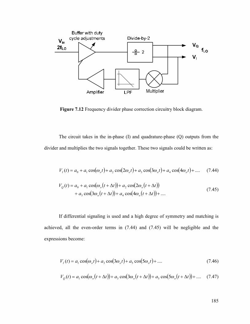
185
Figure 7.12 Frequency divider phase correction circuitry block diagram.
The circuit takes in the in-phase (I) and quadrature-phase (Q) outputs from the
divider and multiplies the two signals together. These two signals could be written as:
( ) ( ) ( ) ( ) ....4cos3cos2coscos)( 43210 +++++= tatatataatV ooooI ωωωω (7.44)
( )( ) ( )( )( )( ) ( )( ) ....4cos3cos
2coscos)(
43
210
+∆++∆++
∆++∆++=
ttattattattaatV
oo
ooQ
ωω
ωω (7.45)
If differential signaling is used and a high degree of symmetry and matching is
achieved, all the even-order terms in (7.44) and (7.45) will be negligible and the
expressions become:
( ) ( ) ( ) ....5cos3coscos)( 531 +++= tatatatV oooI ωωω (7.46)
( )( ) ( )( ) ( )( ) ....5cos 3coscos)( 531 +∆++∆++∆+= ttattattatV oooQ ωωω (7.47)

186
Multiplication of (7.46) and (7.47) gives:
( ) ( ) ( )( ) ( ) ( )( )( ) ( )( ) ( ) ( )( ) ..3cos3coscos3cos
3coscoscoscos)(2331
3121
+∆++∆++
∆++∆+=
tttatttaa
tttaatttatVtV
oooo
ooooIQ
ωωωω
ωωωω (7.48)
Assuming that all the sinusoidal terms will be filtered out later by an integrator
or a low-pass filter, we can then focus on the DC components of (7.48). These DC
components can be expressed as:
( ) ( ) ( ) ( ) ...5cos213cos
21cos
21)( 2
523
21 +∆+∆+∆= tatatatVtV oooDCIQ ωωω (7.49)
In an ideal case, the quadrature-phase signal (VQ) is shifted from the in-phase
signal (VI) by 90° for the fundamental tone (ωo tone), hence we have:
2π
ω =∆ idealo t
oidealt
ωπ
2=∆ (7.50)
If we define δ as the deviation of ∆t from the ideal value, the expression of ∆t
can be expressed as:

187
δωπ
δ +=+∆=∆o
idealtt2
(7.51)
Using (7.49) and (7.51), we then get:
( ) ( ) ( ) ( ) ...5sin213sin
21sin
21)( 2
523
21 +−+−= δωδωδω oooDCIQ aaatVtV (7.52)
If ωoδ is small (for example, less than 10°), (7.52) could be estimated as in
(7.53). Note that higher-order terms (7ωoδ or higher) might be grossly overestimated but
can be neglected in certain cases depending on the values of an. (for example, in the case
of a square wave where a7 is 1/7):
( ) ( ) ( ) ( ) ...25
23
21)( 2
523
21 +−+−≈ δωδωδω oooDCIQ aaatVtV (7.53)
If VQ(t) and VI(t) are square waves, which is a good approximation in most
cases, we then get:
( ) ( ) ( ) ( ) ( )
( )δω
δωδωδωδω
o
ooooSquareDCIQ
K
tVtV
1
,
-
...141
101
61
21)(
=
−+−+−≈ (7.54)
where K1 is a finite positive coefficient. This means that the DC portion of the
multiplier output voltage is proportional to δ with negative coefficient.

188
The delay correction circuitry could be implemented in different ways as long as
it can adjust the zero-crossing points of the divider input signal. In this particular
implementation, the delay is corrected by adjusting the rise and fall time of the inverters
used in a buffering stage before the divider. The simplified schematic of the adjustment
mechanism is shown in figure 7.13 below.
Vin2fLO Vout
VDD
Cload
Vcontrol
M1
M2
M3
Figure 7.13 An inverter with a delay adjustment circuitry.
In figure 7.13, the pull-down resistance is a series combination of the on-
resistance of M1 and the on-resistance of M2. During the pull-down, the gate of M1 is
tied to VDD while the gate of M2 is tied to a control voltage Vcontrol. Assuming a square
law, the on-resistance of a MOS transistor in triode mode is given by:
( )thControl
ON
VVL
WkR
−=
'
1 (7.55)

189
where k’ is a constant that depends on the process technology. W and L are the width
and length of the transistor. If the control voltage consists of a “static” part (VC) and
dynamic part (vc), the pull-down resistance could be:
( )cthD
ON
vVVL
WkR
−−=
'
1 (7.56)
( )cOD
ON
vVL
WkR
−=
'
1 (7.57)
where VOD is the overdrive voltage of the transistor. The total on-resistance of the
combined pull-down path will be:
( )cOD
pull
vVL
WkRR
−+=
'1
1 (7.58)
Since the time delay in pull-up and pull-down is linearly proportional to the
capacitance and resistance of the pull-down path, we can then write:
( )
−+=
cOD
pulldown
vVL
WkRKT
'1
1 (7.59)

190
where Kpull depends on the output capacitance of the stage and the characteristics of the
input signals. If we define downt∆ as the deviation of pull-down time from the case when
vc=0, we then get:
( )
+−
−+=∆
OD
pull
cOD
pulldown
VL
WkRK
vVL
WkRKt
'1
'1
11 (7.60)
+−
++≈∆
OD
pullOD
c
OD
pulldown
VL
WkRK
Vv
VL
WkRKt
'1
'1
111
cdelay
OD
cpulldown vK
VL
Wk
vKt =≈∆
2' (7.61)
Using (7.54) and (7.61), we can draw a simplified mathematical model of the
phase correction loop, as shown in figure 7.14.
Figure 7.14 A simplified model of the IQ phase correction loop

191
Although this diagram ignores the frequency response that controls the dynamics
of the loop, it captures the main part of the loop that regulates the phase error. The
closed-loop DC transfer function, from the phase error at the input to the phase error at
the output, is given by:
odelayin
out
KKt ωδ
111
+=
∆ (7.62)
From (7.62), it is clear that a lower phase error could be achieved by increasing
loopgain. Since this is a feedback system, loop stability could be an issue and should be
considered in the design. In this work, the frequency response is compensated by
placing a dominant RC pole at the output of the IQ multiplier. In addition, the accuracy
of the compensation is affected by mismatches and compensation of devices in the
system, especially the comparison devices (the IQ multiplier and the first amplifier
afterwards). In the final implementation, this phase correction could be turned off
entirely using a digital bit.
7.4 Experimental Results
The circuit was fabricated in a 0.13 µm CMOS technology provided by Infineon
Technologies, and the die microphotograph is shown in figure 7.15. The chip size
including all pads is 1.5 mm x 1.5 mm. Active areas for the LNA, mixer core, and
dividers are approximately 0.1 mm2 in total, and the transimpedance amplifiers occupy
0.6 mm2.

192
Measurements were done on a PCB with encapsulated chip-on-board. The board
has differential RF inputs and differential 2fLO inputs. Off-board baluns were used to
provide differential drives. At the output of the receiver, a differential-to-single-ended
buffer was added to isolate the loading effects seen in the mixer output stage. These
buffers were implemented using ADA4899-1 chips from analog devices [7.9]. The test
boards were built with FR4 material. Figure 7.16 shows a complete photograph of the
assembled test board.
Figure 7.15 Die microphotograph

193
The chip consumes 32 mA at 0.5 GHz fLO and 35 mA at 2.5 GHz fLO from a 1.5
V voltage supply including all the currents drawn from bias circuitry. The 2fLO signal
needs to be -5 dBm at 1 GHz and 10 dBm at 5 GHz in order to maintain front-end
functionality. These power levels are measured at the SMA connector inputs. The
divider works up to 5.2 GHz (2.6 GHz output).
Figure 7.16 Assembled test board
Figure 7.17 shows plots of the input S11 referring to a 100 Ω differential source
impedance. The S11 measurements were done in both high-gain and low-gain modes.
For the high-gain mode, S11 matches better than -10 dB from 0.5 GHz to 3.8 GHz. In the
low-gain mode, S11 matches better than -7 dB up to 3.6 GHz. The S11 results include
parasitics due to the connector and test boards. The results suggest that the designed
front-end would not need any off-chip matching components except a balun or a band-
pass filter that are required for the intended application.

194
Figure 7.18 shows conversion gain (in high-gain mode) at a function of LO
frequency for baseband frequencies of 1 MHz with a 3 dB bandwidth setting of 2 MHz.
The results include variations due to impedance mismatches at the LNA inputs. The
voltage gain of the front-end is approximately 3 dB lower than the power gain.
-25
-20
-15
-10
-5
0
0 0.5 1 1.5 2 2.5 3 3.5 4 4.5 5Frequency (GHz)
S11
(dB
)
High Gain
Low Gain
Figure 7.17 S11 of the receiver in both gain modes
Figure 7.19 shows conversion gain plots against baseband frequency at different
bandwidth settings. The LO frequency in this measurement is fixed at 1.5 GHz, and the
baseband 3-dB bandwidth can be tuned from 1 MHz to 5 MHz. In addition, harmonic
mixing was measured with 2 GHz RF input signal while varying the LO frequency to
have harmonics located at 2 GHz. The conversion gains of 3fLO, 5fLO, and 7fLO are
9.5 dB, 14 dB, and 17 dB below the conversion gain at fLO, respectively.
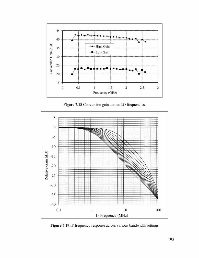
195
15
20
25
30
35
40
45
0 0.5 1 1.5 2 2.5 3
Con
vers
ion
Gai
n (d
B)
Frequency (GHz)
High Gain
Low Gain
Figure 7.18 Conversion gain across LO frequencies.
-40
-35
-30
-25
-20
-15
-10
-5
0
5
0.1 1 10 100
Rel
ativ
e Gai
n (d
B)
IF Frequency (MHz)
Figure 7.19 IF frequency response across various bandwidth settings

196
The in-band two-tone third-order input intercept point (IIP3) was done with input
tones at 330 kHz and 230 kHz offsets from fLO of 1.5 GHz. The normal IIP3 is -6.5 dBm
while the tuned IIP3 is +4 dBm as shown in figure 7.20. The out-of-band IIP3 was
measured with input tones at 4 MHz and 8.2 MHz, and the normal value is -7 dBm. In
low-gain mode, the normal IIP3 is +4 dBm for both in-band and out-of-band tones.
The measured in-band IIP2 with the tones at 330 kHz and 230 kHz offsets is
+48 dBm, while the out-of-band IIP2 with the tones at 4 MHz and 4.2 MHz offsets is
+60 dBm. IIP2 in low-gain mode is higher than +80 dBm. The measurements become
increasingly difficult as IIP2 increases, due to limitations in the dynamic range of the test
equipment. Also, it is possible that the measured in-band IIP2 is limited by the on-board
buffers or the spectrum analyzer.
Noise was measured at various LO and RF frequencies using a noise figure
meter. At 1.5 GHz fLO and 1 MHz baseband, the measured double-sideband noise figure
(DSB NF) is 5.8 dB including all the balun, cable, board losses, and input mismatches.
The estimated loss of the balun and cable (obtained from separate cable and balun
measurements using a network analyzer) is 2.2 dB, and the de-embedded DSB NF is
5.8 dB – 2.2 dB = 3.6 dB. The 3.6 dB DSB NF still includes any board and SMA
connector losses, since it is not possible to directly measure the loss on the PCB. Plots
of de-embedded NF versus baseband for various RF bands are shown in figure 7.21.
DSB NF is approximately 18 dB at 1.5 GHz RF and 1 MHz baseband offset in the low-
gain mode.

197
-100
-80
-60
-40
-20
0
20
40
60
-50 -40 -30 -20 -10 0 10
Output Power (dBm)
Input Power (dBm)
Fundamental
IM3
Figure 7.20 IM3 plot for IIP3 calculations of the circuit
3.2
3.4
3.6
3.8
4.0
4.2
0 2 4 6 8 10
DSB
NF
(dB
)
Baseband Frequency (MHz)
2 GHz
0.5 GHz
1.0 GHz
1 GHz
2.5 GHz
Figure 7.21 De-embedded DSB-NF at various frequencies

198
Figure 7.22 shows the plot of measured LO leakage at the RF port in high-gain
mode, which is below -100 dBm for an entire operating frequency range. During the
measurements, the LO leakage does not change with gain mode, implying that it is not
dominated by the signal path isolation but rather by other mechanisms such as supply
and ground coupling.
-130-125-120-115-110-105-100-95-90
0 0.5 1 1.5 2 2.5 3
LO P
ower
at th
e RF
Port
(dB
m)
LO frequeny ( GHz)
Figure 7.22 Measured LO-RF leakage at various frequencies.
7.5 References
[7.1] J.-H.C. Zhan and S.S. Taylor, “A 5GHz Resistive-Feedback CMOS LNA for
Low-Cost Multi-Standard Applications,” ISSCC Dig. Tech. Papers, pp. 200-201,
Feb. 2006.
[7.2] S.C. Blaakmeer et al., “An Inductorless Wideband Balun-LNA in 65nm CMOS
with balanced output, Proc. ESSCIRC, pp. 364-367, Sept., 2007.

199
[7.3] P. R. Gray, R.G. Meyer, P. J. Hurst, and S. H. Lewis. Analysis and Design of
Analog Integrated Circuits, Fourth Edition, Wiley, New York, 2001.
[7.4] B. Kim, J.-S. Ko, and K. Lee, “A New Linearization Technique for MOSFET
RF Amplifier Using Multiple Gated Transistors,” IEEE Microw. Guided Wave
Lett., vol. 10, no. 9, pp. 371–373, Sep. 2000.
[7.5] T. Kim, B. Kim, and K. Lee, “Highly Linear Receiver Front-End Adopting
MOSFET Transconductance Linearization by Multiple Gated Transistors,” IEEE
J. Solid-State Circuits, vol. 39, Jan. 2004, pp. 223-229.
[7.6] N. Poobuapheun, W-H. Chen, Z. Boos, A. M. Niknejad, “A 1.5 V 0.7-2.5GHz
CMOS Quadrature Demodulator for Multi-Band Direct-Conversion Receivers,”
IEEE J. Solid-State Circuits, vol. 42, Aug. 2007, pp. 1669-1677.
[7.7] Ilku Nam, et al., “CMOS RF Amplifier and Mixer Circuits Utilizing
Complementary Characteristics of Parallel Combined NMOS and PMOS
Devices,” IEEE Transactions on Microwave Theory and Techniques, vol. 53,
Issue 5, pp. 1662-1671, May 2005.
[7.8] S. Navid, F. Behbahani, A. Hajimiri, R. Gaethke, and M. Delurio, “Level-
Locked Loop, A Technique for Broadband Quadrature Signal Generation,” in
Proc. IEEE Custom Integrated Circuits Conf., pp. 411-414, May 1997.
[7.9] http://www.analog.com/en/prod/0,,759_786_ADA4899%252D1,00.html
200
8
Conclusion
8.1 Introduction
This research focused on issues surrounding the design of a multi-band, multi-
standard receiver, specifically, a wideband LNA and mixer designs that cover all
frequency bands from 0.7–2.5 GHz. This chapter summarizes the work presented in this
dissertation and concludes with a discussion of future research topics.
8.2 Summary and Contributions
In Chapter 2 we reviewed receiver fundamentals, starting with the concepts of
selectivity and sensitivity, followed by a review of basic receiver architectures,
including homodyne and heterodyne. We also compared several receiver architectures
for multi-band receivers that use broadband front-ends. A promising way to implement
such a receiver is with multiple broadband receiver front-ends, each of which covers a
group of frequencies in an allocated sub-band. This yields a good compromise without
using multiple narrow-band front-ends, which would occupy a large area; or using a
broadband front-end, which would be susceptible to high levels of out-of-band
interference. We also discussed requirements and estimated performance.

201
Chapter 3 reviewed noise sources, basic LNA architectures, and advanced
architectures for multi-band operations. Chapter 4 presented the design of the broadband
CMOS LNA, which was fabricated and measured in an IBM 0.18 µm technology
process. The LNA achieves -3 dB bandwidth from 1–2 GHz with 16 mA bias current
and 17 dB peak voltage gain. The noise figure is below 4 dB for the same input
frequency range and bias current, with a minimum value of 2.7 dB around 1.2 GHz. The
LNA has -10 dB or better input matching for the entire bandwidth range, even if the bias
current varies from 2–16 mA. As a result, it is suitable for dynamic broadband operation
in multi-band, multi-mode receivers.
We found some discrepancies between simulations and measurement results of
the LNA. A major problem is the accuracy of noise modeling. Because the gate noise is
not accurately modeled in the modeled transistor, its noise contribution could be
considerably underestimated. In addition, the frequency response mismatches might
result from unexpected parasitics causing narrow LNA bandwidth, as observed in the
measurements. These problems can be solved by careful layout, modeling, and parasitic
calculations.
In Chapter 5 we discussed basic concepts of the mixer, important mixer
specifications, mixer implementations in CMOS technologies, and quadrature signal
generation. The best way to implement a mixer is by using switches, which can be
implemented easily using MOS transistors. Compared to its single-balanced counterpart,
a double-balanced mixer (either passive or active) performs better in key areas such as
port isolation and IM2. However, a single-balance mixer is simpler, consumes less
current, and should be used when the specifications can be met. In addition, because of

202
the high level of 1/f noise in CMOS devices, a passive mixer has strong advantages for
use in direct-conversion receivers.
Quadrature signal generation is essential in any receivers that use quadrature
demodulation. There are several ways to obtain quadrature signals, including divide-by-
two circuits, a quadrature-coupled oscillator, and polyphone filters. The choice is driven
primarily by the process technology (device speed and process variations), operating
frequency/frequencies, and power consumption requirements.
Chapter 6 presented an analysis and design of a low 1/f noise inductorless
quadrature demodulator. We used a fully differential complementary pair to increase the
efficiency of the transconductance. The circuit operates over a wide range of
frequencies, including the 0.7–2.5 GHz frequency bands. Mixer gain can be reduced and
linearity can be increased by reducing the feedback impedance of the transimpedance
stage at the mixer output, at the cost of increasing the noise figure in the system. The
feedback resistors and capacitors can be made programmable by using MOS switches,
which also increases design flexibility.
Chapter 7 covered the design and analysis of a wideband receiver front-end in
0.13 µm CMOS technology. The front-end employs a wideband resistive feedback LNA
with gain adjustments. A source-follower stage was inserted between the LNA and the
mixer to increase electrical reverse isolation and reduce LO leakage from the mixer to
the LNA input. The mixer architecture is similar to the one presented in Chapter 6, but
uses multi-gated transistors at the mixer transconductance stage. The multi-gated
topology permits tuning to increase front-end linearity without bias current penalties.
The front-end operates from 0.3–2.6 GHz with a 1–5 MHz baseband bandwidth. The

203
chip employs no inductors and achieves a conversion voltage gain of 38 dB with a 3.6
dB DSB noise figure. The default IIP3 of -6.5 dBm can be increased to +4 dBm in high-
gain mode when the circuit is properly tuned. In addition, the circuit achieves +48 dBm
IIP2 in high-gain mode. The chip consumes 32–35 mA from a 1.5 V supply.
An important consideration when implementing an integrated front-end using the
architecture presented in Chapters 6 and 7 is that in most receivers, the LO is generated
with an integrated voltage-controlled oscillator (VCO), which must be designed
properly to minimize LO leakage into other parts of the circuits; this could cause
dynamic DC offsets. This issue can be alleviated by choosing a VCO running frequency
that is not an integer multiple of fLO, as shown in [8.1].
8.3 Future Research Opportunities
This research focuses on designing high-performance, front-end building blocks,
including low-noise amplifiers (LNA) and downconversion mixers, and does not cover
the implementation of a complete receiver. Challenges remain in designing a completely
reconfigurable, low-cost, multi-band, multi-standard receiver chip, at both the system
and circuit levels.
For example, such a receiver would require a highly reconfigurable frequency
synthesizer that can be adjusted for different output frequencies, loop bandwidths, and
phase noise levels. Designing such a synthesizer with the lowest possible cost in CMOS
technologies would be an interesting research topic.
Another interesting topic for research would be the high-level implementation of
a complete front-end to improve overall noise, linearity, and selectivity. For example,

204
the mixer presented in Chapters 6 and 7 exhibits a high level of harmonic conversion
gain (from 3fLO, 5fLO, etc. down to near DC). This results in high output noise because
of noise folding, and very high reciprocal mixing from a blocker at the harmonic
frequency bands. In this case, the mixer architecture presented in [8.2] could be utilized
to achieve harmonic rejection.
Finally, the front-end circuit presented in Chapter 7 has several tuning
mechanisms in both analog and digital. However, all the tuning must be done manually
by external control. A research topic on designing a low-cost, multi-band, mixed-signal
front-end with digital interface and calibration would make significant contributions to
this field of study.
8.4 References
[8.1] A. Behzad, et al., “Direct-conversion CMOS transceiver with automatic
frequency control for 802.11a wireless LANs,” in IEEE Int. Solid-State Circuits
Conf. Dig. Tech. Papers, San Francisco, CA, Feb. 2003, pp. 356-499.
[8.2] J. Weldon, et al., “A 1.75-GHz highly integrated narrow-band CMOS transmitter
with harmonic-rejection mixers,” IEEE J. Solid-State Circuits, vol. 36, no. 12,
pp. 2003-2015, December 2001.