LM70 SPI/MICROWIRE 10-Bit plus Sign Digital …edge.rit.edu/content/P07202/public/Electrical/Data...
14
LM70 SPI/MICROWIRE 10-Bit plus Sign Digital Temperature Sensor General Description The LM70 is a temperature sensor, Delta-Sigma analog-to- digital converter with an SPI and MICROWIRE compatible interface available in LLP and MSOP 8-pin packages. The host can query the LM70 at any time to read temperature. A shutdown mode decreases power consumption to less than 10 μA. This mode is useful in systems where low average power consumption is critical. The LM70 has 10-bit plus sign temperature resolution (0.25˚C per LSB) while operating over a temperature range of -55˚C to +150˚C. The LM70’s 2.65V to 5.5V supply voltage range, low supply current and simple SPI interface make it ideal for a wide range of applications. These include thermal management and protection applications in hard disk drives, printers, elec- tronic test equipment, and office electronics. Applications n System Thermal Management n Personal Computers n Disk Drives n Office Electronics n Electronic Test Equipment Features n 0.25˚C temperature resolution. n Shutdown mode conserves power between temperature reading n SPI and MICROWIRE Bus interface n MSOP-8 and LLP-8 packages save space n UL Recognized Component Key Specifications j Supply Voltage 2.65V to 5.5V j Supply Current operating 260 μA (typ) 490 μA (max) shutdown 12 μA (typ) j Temperature Accuracy -40˚C to 85˚C ±2˚C(max) -10˚C to 65˚C +1.5/-2˚C(max) -55˚C to 125˚C +3/-2˚C(max) -55˚C to 150˚C +3.5/-2˚C(max) Simplified Block Diagram 10122301 February 2006 LM70 SPI/MICROWIRE ™ 10-Bit plus Sign Digital Temperature Sensor © 2006 National Semiconductor Corporation DS101223 www.national.com
Transcript of LM70 SPI/MICROWIRE 10-Bit plus Sign Digital …edge.rit.edu/content/P07202/public/Electrical/Data...

LM70SPI/MICROWIRE 10-Bit plus Sign Digital TemperatureSensorGeneral DescriptionThe LM70 is a temperature sensor, Delta-Sigma analog-to-digital converter with an SPI and MICROWIRE compatibleinterface available in LLP and MSOP 8-pin packages. Thehost can query the LM70 at any time to read temperature. Ashutdown mode decreases power consumption to less than10 µA. This mode is useful in systems where low averagepower consumption is critical.
The LM70 has 10-bit plus sign temperature resolution(0.25˚C per LSB) while operating over a temperature rangeof −55˚C to +150˚C.
The LM70’s 2.65V to 5.5V supply voltage range, low supplycurrent and simple SPI interface make it ideal for a widerange of applications. These include thermal managementand protection applications in hard disk drives, printers, elec-tronic test equipment, and office electronics.
Applicationsn System Thermal Managementn Personal Computersn Disk Drivesn Office Electronicsn Electronic Test Equipment
Featuresn 0.25˚C temperature resolution.n Shutdown mode conserves power between temperature
readingn SPI and MICROWIRE Bus interfacen MSOP-8 and LLP-8 packages save spacen UL Recognized Component
Key Specificationsj Supply Voltage 2.65V to 5.5V
j Supply Current operating 260 µA (typ)
490 µA (max)
shutdown 12 µA (typ)
j TemperatureAccuracy
−40˚C to 85˚C ±2˚C(max)
−10˚C to 65˚C +1.5/−2˚C(max)
−55˚C to 125˚C +3/−2˚C(max)
−55˚C to 150˚C +3.5/−2˚C(max)
Simplified Block Diagram
10122301
February 2006LM
70S
PI/M
ICR
OW
IRE
™10-B
itplus
Sign
DigitalTem
peratureS
ensor
© 2006 National Semiconductor Corporation DS101223 www.national.com

Connection DiagramsMSOP-8 LLP-8
10122302
TOP VIEWNS Package Number MUA08A
10122325
TOP VIEWNS Package Number LDA08A
Ordering Information
Order NumberPackageMarking
NS PackageNumber
Supply Voltage Transport Media
LM70CILD-3 T33 LLP-8, LDA08A 2.65V to 3.6V 1000 Units in Tape and Reel
LM70CILDX-3 T33 LLP-8, LDA08A 2.65V to 3.6V 4500 Units in Tape and Reel
LM70CILD-5 T35 LLP-8, LDA08A 4.5V to 5.5V 1000 Units in Tape and Reel
LM70CILDX-5 T35 LLP-8, LDA08A 4.5V to 5.5V 4500 Units in Tape and Reel
LM70CIMM-3 T04C MSOP-8, MUA08A 2.65V to 3.6V 1000 Units in Tape and Reel
LM70CIMMX-3 T04C MSOP-8, MUA08A 2.65V to 3.6V 3500 Units in Tape and Reel
LM70CIMM-5 T03C MSOP-8, MUA08A 4.5V to 5.5V 1000 Units in Tape and Reel
LM70CIMMX-5 T03C MSOP-8, MUA08A 4.5V to 5.5V 3500 Units in Tape and Reel
Pin Descriptions
Label SOP-8Pin #
LLP-8Pin #
Function Typical Connection
SI/O 1 1 Input/Output - Serial bus bi-directional data line.Schmitt trigger input.
From and to Controller
SC 2 3 Clock - Serial bus clock Schmitt trigger inputline.
From Controller
GND 4 7 Power Supply Ground Ground
V+ 5 5 Positive Supply Voltage Input DC Voltage from 2.65V to 5.5V. Bypasswith a 0.1 µF ceramic capacitor.
CS 7 8 Chip Select input. From Controller
NC 3, 6, 8 2, 4, 6 No Connect These pins are not connected to theLM70 die in any way.
LM70
www.national.com 2

Typical Application
10122303
FIGURE 1. COP Microcontroller Interface
LM70
www.national.com3
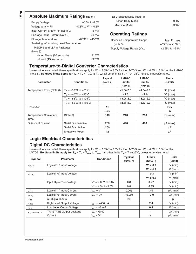
Absolute Maximum Ratings (Note 1)
Supply Voltage −0.3V to 6.0V
Voltage at any Pin −0.3V to V+ + 0.3V
Input Current at any Pin (Note 2) 5 mA
Package Input Current (Note 2) 20 mA
Storage Temperature −65˚C to +150˚C
Soldering Information, Lead Temperature
MSOP-8 and LLP-8 Packages(Note 3)
Vapor Phase (60 seconds)Infrared (15 seconds)
215˚C220˚C
ESD Susceptibility (Note 4)
Human Body Model 3000V
Machine Model 300V
Operating RatingsSpecified Temperature Range TMIN to TMAX
(Note 5) −55˚C to +150˚C
Supply Voltage Range (+VS) +2.65V to +5.5V
Temperature-to-Digital Converter CharacteristicsUnless otherwise noted, these specifications apply for V+ = 2.65V to 3.6V for the LM70-3 and V+ = 4.5V to 5.5V for the LM70-5(Note 6). Boldface limits apply for TA = TJ = TMIN to TMAX; all other limits TA = TJ=+25˚C, unless otherwise noted.
Parameter ConditionsTypical(Note 7)
LM70-5Limits
(Note 8)
LM70-3Limits
(Note 8)
Units(Limit)
Temperature Error (Note 6) TA = −10˚C to +65˚C +1.5/−2.0 +1.5/−2.0 ˚C (max)
TA = −40˚C to +85˚C ±2.0 ±2.0 ˚C (max)
TA = −55˚C to +125˚C +3.0/−2.0 +3.0/−2.0 ˚C (max)
TA = −55˚C to +150˚C +3.5/−2.0 +3.5/−2.0 ˚C (max)
Resolution 110.25
Bits˚C
Temperature ConversionTime
(Note 9) 140 210 210 ms (max)
Quiescent Current Serial Bus Inactive 260 490 490 µA (max)
Serial Bus Active 260 µA
Shutdown Mode 12 µA
Logic Electrical CharacteristicsDigital DC CharacteristicsUnless otherwise noted, these specifications apply for V+ = 2.65V to 3.6V for the LM70-3 and V+ = 4.5V to 5.5V for theLM70-5. Boldface limits apply for TA = TJ = TMIN to TMAX; all other limits TA = TJ=+25˚C, unless otherwise noted.
Symbol Parameter ConditionsTypical(Note 7)
Limits(Note 8)
Units(Limit)
VIN(1) Logical “1” Input Voltage V+ x 0.7 V (min)
V+ + 0.3 V (max)
VIN(0) Logical “0” Input Voltage −0.3 V (min)
V+ x 0.3 V (max)
Input Hysteresis Voltage V+ = 2.65V to 3.6V 0.8 0.27 V (min)
V+ = 4.5V to 5.5V 0.8 0.35 V (min)
IIN(1) Logical “1” Input Current VIN = V+ 0.005 3.0 µA (max)
IIN(0) Logical “0” Input Current VIN = 0V −0.005 −3.0 µA (min)
CIN All Digital Inputs 20 pF
VOH High Level Output Voltage IOH = −400 µA 2.4 V (min)
VOL Low Level Output Voltage IOL = +2 mA 0.4 V (max)
IO_TRI-STATE TRI-STATE Output LeakageCurrent
VO = GNDVO = V+
−1+1
µA (min)µA (max)
LM70
www.national.com 4

Logic Electrical Characteristics (Continued)
Serial Bus Digital Switching CharacteristicsUnless otherwise noted, these specifications apply for V+ = 2.65V to 3.6V for the LM70-3 and V+ = 4.5V to 5.5V for theLM70-5, CL (load capacitance) on output lines = 100 pF unless otherwise specified. Boldface limits apply for TA = TJ = TMIN
to TMAX; all other limits TA = TJ = +25˚C, unless otherwise noted.
Symbol Parameter ConditionsTypical(Note 7)
Limits(Note 8)
Units(Limit)
t1 SC (Clock) Period 0.16DC
µs (min)(max)
t2 CS Low to SC (Clock) High Set-Up Time 100 ns (min)
t3 CS Low to Data Out (SO) Delay 70 ns (max)
t4 SC (Clock) Low to Data Out (SO) Delay 70 ns (max)
t5 CS High to Data Out (SO) TRI-STATE 200 ns (min)
t6 SC (Clock) High to Data In (SI) Hold Time 60 ns (min)
t7 Data In (SI) Set-Up Time to SC (Clock) High 30 ns (min)
Timing Diagrams
10122304
FIGURE 2. Data Output Timing Diagram
10122305
FIGURE 3. TRI-STATE Data Output Timing Diagram
10122306
FIGURE 4. Data Input Timing Diagram
LM70
www.national.com5

Electrical CharacteristicsNote 1: Absolute Maximum Ratings indicate limits beyond which damage to the device may occur. DC and AC electrical specifications do not apply when operatingthe device beyond its rated operating conditions.
Note 2: When the input voltage (VI) at any pin exceeds the power supplies (VI < GND or VI > +VS) the current at that pin should be limited to 5 mA. The 20 mAmaximum package input current rating limits the number of pins that can safely exceed the power supplies with an input current of 5 mA to four.
Note 3: See the section titled “Surface Mount” found in a current National Semiconductor Linear Data Book for other methods of soldering surface mount devices.
Note 4: Human body model, 100 pF discharged through a 1.5 kΩ resistor. Machine model, 200 pF discharged directly into each pin.
Note 5: The life expectancy of the LM70 will be reduced when operating at elevated temperatures. LM70 θJA (thermal resistance, junction-to-ambient) whenattached to a printed circuit board with 2 oz. foil is summarized in the table below:
Device NumberNS Package
NumberThermal
Resistance (θJA)
LM70CILD LDA08A 51.3˚C/W
LM70CIMM MUA08A 200˚C/W
Note 6: Both part numbers of the LM70 will operate properly over the V+ supply voltage range of 2.65V to 5.5V. The temperature error for temperature ranges of−10˚C to +65˚C, −40˚C to +85˚C, −55˚C to +125˚C and −55˚C to +150˚C include error induced by power supply variation of ±5% from the nominal value.Temperature error will increase by ±0.3˚C for a power supply voltage (V+) variation of ±10% from the nominal value.
Note 7: Typicals are at TA = 25˚C and represent most likely parametric norm.
Note 8: Limits are guaranteed to National’s AOQL (Average Outgoing Quality Level).
Note 9: This specification is provided only to indicate how often temperature data is updated. The LM70 can be read at any time without regard to conversion state(and will yield last conversion result). A conversion in progress will not be interrupted. The output shift register will be updated at the completion of the read and anew conversion restarted.
Note 10: For best accuracy, minimize output loading. Higher sink currents can affect sensor accuracy with internal heating. This can cause an error of 0.64˚C at fullrated sink current and saturation voltage based on junction-to-ambient thermal resistance.
LM70
www.national.com 6

Electrical Characteristics (Continued)
TRI-STATE Test Circuit
10122308
FIGURE 5. Temperature-to-Digital Transfer Function (Non-linear scale for clarity)
10122307
FIGURE 6.
LM70
www.national.com7

Typical Performance CharacteristicsAverage Power-On Reset Voltage vs Temperature Static Supply Current vs Temperature
10122323 10122321
Temperature Error
10122322
LM70
www.national.com 8

1.0 Functional DescriptionThe LM70 temperature sensor incorporates a band-gap typetemperature sensor and 10-bit plus sign ∆Σ ADC (Delta-Sigma Analog-to-Digital Converter). Compatibility of theLM70’s three wire serial interface with SPI and MICROWIREallows simple communications with common microcontrol-lers and processors. Shutdown mode can be used to opti-mize current drain for different applications. A manufacture’sID register identifies the LM70 as National Semiconductorproduct.
1.1 POWER UP AND POWER DOWN
The LM70 always powers up in a known state. The power updefault condition is continuous conversion mode. Immediatlyafter power up the LM70 will output an erroneous code untilthe first temperature conversion has completed.
When the supply voltage is less than about 1.6V (typical),the LM70 is considered powered down. As the supply volt-age rises above the nominal 1.6V power up threshold, theinternal registers are reset to the power up default statedescribed above.
1.2 SERIAL BUS INTERFACE
The LM70 operates as a slave and is compatible with SPI orMICROWIRE bus specifications. Data is clocked out on thefalling edge of the serial clock (SC), while data is clocked inon the rising edge of SC. A complete transmit/receive com-munication will consist of 32 serial clocks. The first 16 clockscomprise the transmit phase of communication, while thesecond 16 clocks are the receive phase.
When CS is high SI/O will be in TRISTATE®. Communicationshould be initiated by taking chip select (CS) low. Thisshould not be done when SC is changing from a low to highstate. Once CS is low the serial I/O pin (SI/O) will transmitthe first bit of data. The master can then read this bit with therising edge of SC. The remainder of the data will be clockedout by the falling edge of SC. Once the 14 bits of data (onesign bit, ten temperature bits and 3 high bits) are transmittedthe SI/O line will go into TRI-STATE. CS can be taken high atany time during the transmit phase. If CS is brought low inthe middle of a conversion the LM70 will complete the con-version and the output shift register will be updated after CSis brought back high.
The receive phase of a communication starts after 16 SCperiods. CS can remain low for 32 SC cycles. The LM70 willread the data available on the SI/O line on the rising edge ofthe serial clock. Input data is to an 8-bit shift register. Thepart will detect the last eight bits shifted into the register. Thereceive phase can last up to 16 SC periods. All ones must beshifted in order to place the part into shutdown. A zero in anylocation will take the LM70 out of shutdown. The followingcodes only should be transmitted to the LM70:
• 00 hex (normal operation)
• 01 hex (normal operation)
• 03 hex (normal operation)
• 07 hex (normal operation)
• 0F hex (normal operation)
• 1F hex (normal operation)
• 3F hex(normal operation)
• 7F hex(normal operation)
• FF hex (Shutdown, transmit manufacturer’s ID)
.
any others may place the part into a Test Mode. Test Modesare used by National Semiconductor to thoroughly test thefunction of the LM70 during production testing. Only eightbits have been defined above since only the last eight trans-mitted, before CS is taken HIGH, are detected by the LM70
The following communication can be used to determine theManufacturer’s/Device ID and then immediately place thepart into continuous conversion mode. With CS continuouslylow:
• Read 16 bits of temperature data
• Write 16 bits of data commanding shutdown
• Read 16 bits of Manufacture’s/Device ID data
• Write 8 to 16 bits of data commanding Conversion Mode
• Take CS HIGH.
Note that 250 ms will have to pass for a conversion tocomplete before the LM70 actually transmits temperaturedata.
1.3 TEMPERATURE DATA FORMAT
Temperature data is represented by a 11-bit, two’s comple-ment word with an LSB (Least Significant Bit) equal to0.25˚C:
Temperature Digital Output
Binary Hex
+150˚C 0100 1011 0001 1111 4B 1Fh
+125˚C 0011 1110 1001 1111 3E 9Fh
+25˚C 0000 1100 1001 1111 0B 9Fh
+0.25˚C 0000 0000 0011 1111 00 3Fh
0˚C 0000 0000 0001 1111 00 1Fh
−0.25˚C 1111 1111 1111 1111 FF FFh
−25˚C 1111 0011 1001 1111 F3 9Fh
−55˚C 1110 0100 1001 1111 E4 9Fh
Note: The last two bits are TRI-STATE and depicted as onein the table.
The first data byte is the most significant byte with mostsignificant bit first, permitting only as much data as neces-sary to be read to determine temperature condition. Forinstance, if the first four bits of the temperature data indicatean overtemperature condition, the host processor could im-mediately take action to remedy the excessive tempera-tures.
1.4 SHUTDOWN MODE/MANUFACTURER’S ID
Shutdown mode is enabled by writing XX FF to the LM70 asshown in Figure 7c and discussed in Section 1.2. The serialbus is still active when the LM70 is in shutdown. Currentdraw drops to less than 10 µA between serial communica-tions. When in shutdown mode the LM70 always will output1000 0001 0000 00XX. This is the manufacturer’s ID/DeviceID information. The first 5-bits of the field (1000 0XXX) arereserved for manufacturer’s ID.
LM70
www.national.com9

1.0 Functional Description (Continued)
1.5 INTERNAL REGISTER STRUCTURE
The LM70 has three registers, the temperature register, theconfiguration register and the manufacturer’s/device identifi-cation register. The temperature and manufacturer’s/deviceidentification registers are read only. The configuration reg-ister is write only.
1.5.1 CONFIGURATION REGISTER
(Selects shutdown or continuous conversion modes):
(Write Only):
D15 D14 D13 D12 D11 D10 D9 D8 D7 D6 D5 D4 D3 D2 D1 D0
X X X X X X X X Shutdown
D0-D15 set to XX FF hex enables shutdown mode.
D0-D15 set to XX 00 hex enables continuous conversionmode.
Note: setting D0-D15 to any other values may place theLM70 into a manufacturer’s test mode, upon which the LM70
will stop responding as described. These test modes are tobe used for National Semiconductor production testing only.See Section 1.2 Serial Bus Interface for a complete discus-sion.
1.5.2 TEMPERATURE REGISTER(Read Only):
D15 D14 D13 D12 D11 D10 D9 D8 D7 D6 D5 D4 D3 D2 D1 D0
MSB Bit 9 Bit 8 Bit 7 Bit 6 Bit 5 Bit 4 Bit 3 Bit 2 Bit 1 LSB 1 1 1 X X
D0–D1: Undefined. TRI-STATE will be output on SI/0.
D2–D4: Always set high.
D5–D15: Temperature Data. One LSB = 0.25˚C. Two’scomplement format.
1.5.3 MANUFACTURER’S/DEVICE ID REGISTER(Read Only):
D15 D14 D13 D12 D11 D10 D9 D8 D7 D6 D5 D4 D3 D2 D1 D0
1 0 0 0 0 0 0 1 0 0 0 0 0 0 X X
D0–D1: Undefined. TRI-STATE will be output on SI/0.
D2-D4: Always set LOW.
D5–D15: Manufacturer’s ID Data. This register is accessedwhenever the LM70 is in shutdown mode.
LM70
www.national.com 10

2.0 Serial Bus Timing Diagrams
3.0 Application HintsTo get the expected results when measuring temperaturewith an integrated circuit temperature sensor like the LM70,it is important to understand that the sensor measures itsown die temperature. For the LM70, the best thermal pathbetween the die and the outside world is through the LM70’spins. In the MSOP-8 package the ground pin is connected tothe back side of the LM70 die and thus has the most effecton the die temperature. Although the other pins will alsohave some effect on the LM70die temperature and thereforeshould not be discounted. The LM70 will provide an accuratemeasurement of the temperature of the printed circuit boardon which it is mounted, because the pins represent a goodthermal path to the die. A less efficient thermal path exists
between the plastic package and the LM70 die. If the ambi-ent air temperature is significantly different from the printedcircuit board temperature, it will have a small effect on themeasured temperature.
In probe-type applications, the LM70 can be mounted insidea sealed-end metal tube, and can then be dipped into a bathor screwed into a threaded hole in a tank. As with any IC, theLM70 and accompanying wiring and circuits must be keptinsulated and dry, to avoid leakage and corrosion. This isespecially true if the circuit may operate at cold temperatureswhere condensation can occur. Printed-circuit coatings andvarnishes such as Humiseal and epoxy paints or dips areoften used to insure that moisture cannot corrode the LM70or its connections.
10122314
a) Reading Continuous Conversion - Single Eight-Bit Frame
10122315
b) Reading Continuous Conversion - Two Eight-Bit Frames
10122318
c) Writing Shutdown Control
FIGURE 7. Timing Diagrams
LM70
www.national.com11

4.0 Typical Applications
10122320
FIGURE 8. Temperature monitor using Intel 196 processor
10122319
FIGURE 9. LM70 digital input control using micro-controller’s general purpose I/O.
LM70
www.national.com 12

Physical Dimensions inches (millimeters) unless otherwise noted
8-Lead Molded Mini Small Outline Package (MSOP)(JEDEC REGISTRATION NUMBER M0-187)
Order Number LM70CIMM-3, LM70CIMMX-3, LM70CIMM-5 or LM70CIMMX-5NS Package Number MUA08A
8-Lead Molded Leadless Leadframe PackageOrder Number LM70CILD-3, LM70CILDX-3, LM70CILD-5 or LM70CILDX-5
NS Package Number LDA08A
LM70
www.national.com13

Notes
National does not assume any responsibility for use of any circuitry described, no circuit patent licenses are implied and National reservesthe right at any time without notice to change said circuitry and specifications.
For the most current product information visit us at www.national.com.
LIFE SUPPORT POLICY
NATIONAL’S PRODUCTS ARE NOT AUTHORIZED FOR USE AS CRITICAL COMPONENTS IN LIFE SUPPORT DEVICES OR SYSTEMSWITHOUT THE EXPRESS WRITTEN APPROVAL OF THE PRESIDENT AND GENERAL COUNSEL OF NATIONAL SEMICONDUCTORCORPORATION. As used herein:
1. Life support devices or systems are devices or systemswhich, (a) are intended for surgical implant into the body, or(b) support or sustain life, and whose failure to perform whenproperly used in accordance with instructions for useprovided in the labeling, can be reasonably expected to resultin a significant injury to the user.
2. A critical component is any component of a life supportdevice or system whose failure to perform can be reasonablyexpected to cause the failure of the life support device orsystem, or to affect its safety or effectiveness.
BANNED SUBSTANCE COMPLIANCE
National Semiconductor manufactures products and uses packing materials that meet the provisions of the Customer ProductsStewardship Specification (CSP-9-111C2) and the Banned Substances and Materials of Interest Specification (CSP-9-111S2) and containno ‘‘Banned Substances’’ as defined in CSP-9-111S2.
Leadfree products are RoHS compliant.
National SemiconductorAmericas CustomerSupport CenterEmail: [email protected]: 1-800-272-9959
National SemiconductorEurope Customer Support Center
Fax: +49 (0) 180-530 85 86Email: [email protected]
Deutsch Tel: +49 (0) 69 9508 6208English Tel: +44 (0) 870 24 0 2171Français Tel: +33 (0) 1 41 91 8790
National SemiconductorAsia Pacific CustomerSupport CenterEmail: [email protected]
National SemiconductorJapan Customer Support CenterFax: 81-3-5639-7507Email: [email protected]: 81-3-5639-7560
www.national.com
LM70
SP
I/MIC
RO
WIR
E™
10-B
itpl
usS
ign
Dig
italT
empe
ratu
reS
enso
r