LM5113 5A, 100V Half-Bridge Gate Driver for Enhancement ...
23
LM5113 www.ti.com SNVS725F – JUNE 2011 – REVISED APRIL 2013 LM5113 5A, 100V Half-Bridge Gate Driver for Enhancement Mode GaN FETs Check for Samples: LM5113 1FEATURES DESCRIPTION 2• Independent High-Side and Low-Side TTL The LM5113 is designed to drive both the high-side Logic Inputs and the low-side enhancement mode Gallium Nitride • 1.2A/5A Peak Source/Sink Current (GaN) FETs in a synchronous buck or a half bridge • High-Side Floating Bias Voltage Rail Operates configuration. The floating high-side driver is capable up to 100VDC of driving a high-side enhancement mode GaN FET operating up to 100V. The high-side bias voltage is • Internal Bootstrap Supply Voltage Clamping generated using a bootstrap technique and is • Split Outputs for Adjustable Turn-on/Turn-off internally clamped at 5.2V, which prevents the gate Strength voltage from exceeding the maximum gate-source • 0.6Ω /2.1Ω Pull-down/Pull-up Resistance voltage rating of enhancement mode GaN FETs. The inputs of the LM5113 are TTL logic compatible, and • Fast Propagation Times (28ns Typical) can withstand input voltages up to 14V regardless of • Excellent Propagation Delay Matching (1.5ns the VDD voltage. The LM5113 has split gate outputs, Typical) providing flexibility to adjust the turn-on and turn-off • Supply Rail Under-Voltage Lockout strength independently. • Low Power Consumption In addition, the strong sink capability of the LM5113 maintains the gate in the low state, preventing TYPICAL APPLICATIONS unintended turn-on during switching. The LM5113 can operate up to several MHz. The LM5113 is • Current Fed Push-Pull converters available in a standard WSON-10 pin package and a • Half and Full-Bridge converters 12-bump DSBGA package. The WSON-10 pin package contains an exposed pad to aid power • Synchronous Buck converters dissipation. The DSBGA package offers a compact • Two-switch Forward converters footprint and minimized package inductance. • Forward with Active Clamp converters PACKAGES • WSON-10 (4 mm x 4 mm) • DSBGA (2 mm x 2 mm) 1 Please be aware that an important notice concerning availability, standard warranty, and use in critical applications of Texas Instruments semiconductor products and disclaimers thereto appears at the end of this data sheet. 2All trademarks are the property of their respective owners. PRODUCTION DATA information is current as of publication date. Copyright © 2011–2013, Texas Instruments Incorporated Products conform to specifications per the terms of the Texas Instruments standard warranty. Production processing does not necessarily include testing of all parameters.
Transcript of LM5113 5A, 100V Half-Bridge Gate Driver for Enhancement ...
LM5113
www.ti.com SNVS725F –JUNE 2011–REVISED APRIL 2013
LM5113 5A, 100V Half-Bridge Gate Driver for Enhancement Mode GaN FETsCheck for Samples: LM5113
1FEATURESDESCRIPTION
2• Independent High-Side and Low-Side TTLThe LM5113 is designed to drive both the high-sideLogic Inputsand the low-side enhancement mode Gallium Nitride
• 1.2A/5A Peak Source/Sink Current (GaN) FETs in a synchronous buck or a half bridge• High-Side Floating Bias Voltage Rail Operates configuration. The floating high-side driver is capable
up to 100VDC of driving a high-side enhancement mode GaN FEToperating up to 100V. The high-side bias voltage is• Internal Bootstrap Supply Voltage Clampinggenerated using a bootstrap technique and is
• Split Outputs for Adjustable Turn-on/Turn-off internally clamped at 5.2V, which prevents the gateStrength voltage from exceeding the maximum gate-source
• 0.6Ω /2.1Ω Pull-down/Pull-up Resistance voltage rating of enhancement mode GaN FETs. Theinputs of the LM5113 are TTL logic compatible, and• Fast Propagation Times (28ns Typical)can withstand input voltages up to 14V regardless of
• Excellent Propagation Delay Matching (1.5ns the VDD voltage. The LM5113 has split gate outputs,Typical) providing flexibility to adjust the turn-on and turn-off
• Supply Rail Under-Voltage Lockout strength independently.• Low Power Consumption In addition, the strong sink capability of the LM5113
maintains the gate in the low state, preventingTYPICAL APPLICATIONS unintended turn-on during switching. The LM5113
can operate up to several MHz. The LM5113 is• Current Fed Push-Pull convertersavailable in a standard WSON-10 pin package and a
• Half and Full-Bridge converters 12-bump DSBGA package. The WSON-10 pinpackage contains an exposed pad to aid power• Synchronous Buck convertersdissipation. The DSBGA package offers a compact• Two-switch Forward convertersfootprint and minimized package inductance.
• Forward with Active Clamp converters
PACKAGES• WSON-10 (4 mm x 4 mm)• DSBGA (2 mm x 2 mm)
1
Please be aware that an important notice concerning availability, standard warranty, and use in critical applications ofTexas Instruments semiconductor products and disclaimers thereto appears at the end of this data sheet.
2All trademarks are the property of their respective owners.
PRODUCTION DATA information is current as of publication date. Copyright © 2011–2013, Texas Instruments IncorporatedProducts conform to specifications per the terms of the TexasInstruments standard warranty. Production processing does notnecessarily include testing of all parameters.
LOH
UVLO
HOHLEVELSHIFT
HB
HS
VDD
VSS
HI
LI
HOL
LOL
UVLO & CLAMP
LM5113
SNVS725F –JUNE 2011–REVISED APRIL 2013 www.ti.com
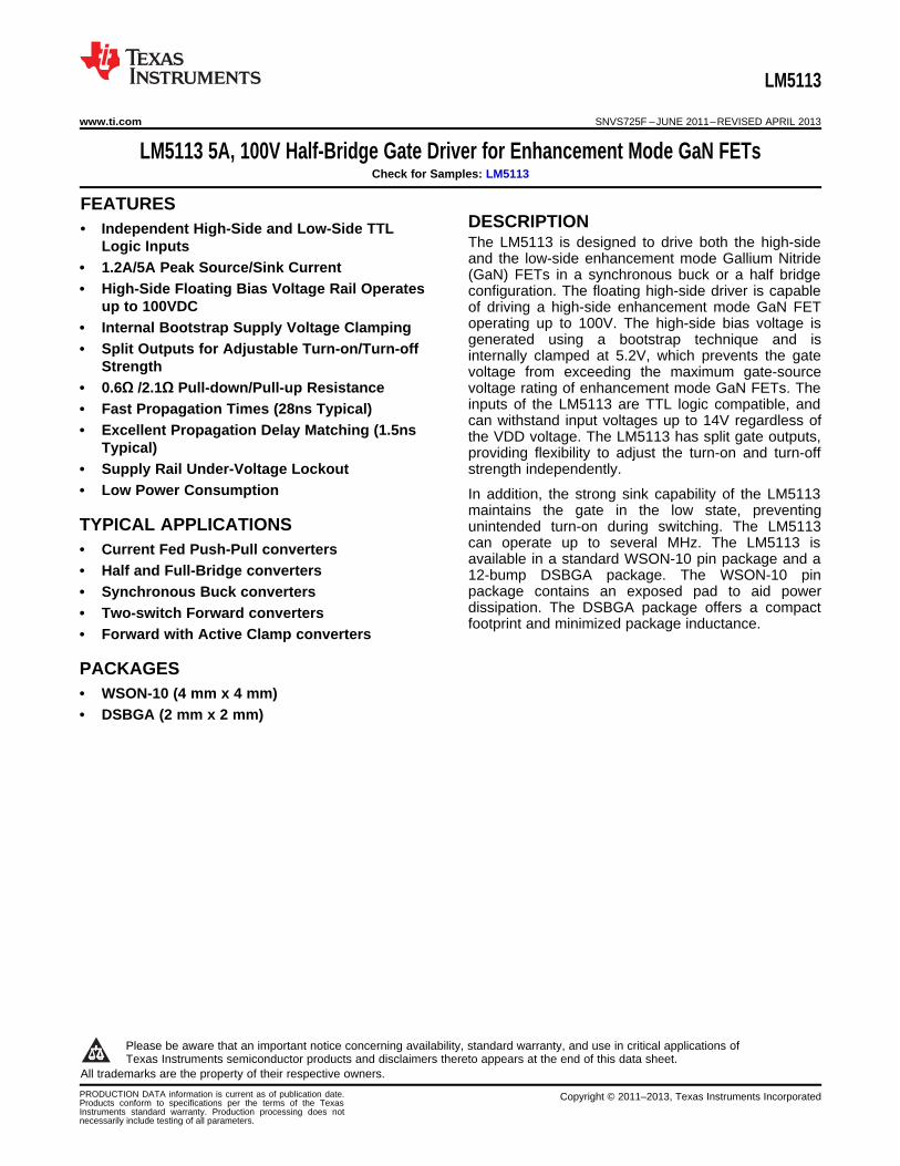
Typical Application
Figure 1.
Truth TableHI LI HOH HOL LOH LOL
L L Open L Open L
L H Open L H Open
H L H Open Open L
H H H Open H Open
2 Submit Documentation Feedback Copyright © 2011–2013, Texas Instruments Incorporated
Product Folder Links: LM5113
VDD LI
HI
VDD
HSHBHOHHOL
HS
LOH
LOL VSSA
B
C
D
1 2 3 4
Top View
VDDLI
HI
VDD
HS HB HOH HOL
HS
LOH
LOLVSS A
B
C
D
1234
Bump Side
1
2
3
4
9
6
7
8
VDD
HB
HOH
HOL
HI
LI
VSS
LOH
HS 5
10
LOL
Exposed Pad
LM5113
www.ti.com SNVS725F –JUNE 2011–REVISED APRIL 2013
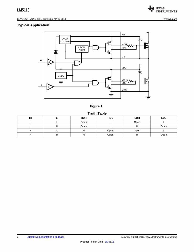
Connection Diagram
Figure 2. WSON PackagePackage Number DPR0010A
DSBGA PackagePackage Number YFX0012FLA
PIN DESCRIPTIONSPin Number Name Description Applications Information
DSBGA WSON-10
A3, C4 (1) 1 VDD 5V Positive gate drive supply Locally decouple to VSS using low ESR/ESLcapacitor located as close to the IC as possible.
D3 2 HB High-side gate driver bootstrap Connect the positive terminal of the bootstraprail capacitor to HB and the negative terminal to HS.
The bootstrap capacitor should be placed asclose to the IC as possible.
D2 3 HOH High-side gate driver turn-on Connect to the gate of high-side GaN FET with aoutput short, low inductance path. A gate resistor can be
used to adjust the turn-on speed.
D1 4 HOL High-side gate driver turn-off Connect to the gate of high-side GaN FET with aoutput short, low inductance path. A gate resistor can be
used to adjust the turn-off speed.
C1, D4 (1) 5 HS High-side GaN FET source Connect to the bootstrap capacitor negativeconnection terminal and the source of the high-side GaN
FET.
B4 6 HI High-side driver control input The LM5113 inputs have TTL type thresholds.Unused inputs should be tied to ground and notleft open.
A4 7 LI Low-side driver control input The LM5113 inputs have TTL type thresholds.Unused inputs should be tied to ground and notleft open.
(1) A3 and C4, C1 and D4 are internally connected.
Copyright © 2011–2013, Texas Instruments Incorporated Submit Documentation Feedback 3
Product Folder Links: LM5113
LM5113
SNVS725F –JUNE 2011–REVISED APRIL 2013 www.ti.com
PIN DESCRIPTIONS (continued)
Pin Number Name Description Applications Information
DSBGA WSON-10
A2 8 VSS Ground return All signals are referenced to this ground.
A1 9 LOL Low-side gate driver sink-current Connect to the gate of the low-side GaN FET withoutput a short, low inductance path. A gate resistor can
be used to adjust the turn-off speed.
B1 10 LOH Low-side gate driver source- Connect to the gate of high-side GaN FET with acurrent output short, low inductance path. A gate resistor can be
used to adjust the turn-on speed.
EP Exposed Pad It is recommended that the exposed pad on thebottom of the package be soldered to groundplane on the PC board to aid thermal dissipation.
These devices have limited built-in ESD protection. The leads should be shorted together or the device placed in conductive foamduring storage or handling to prevent electrostatic damage to the MOS gates.
Absolute Maximum Ratings (1)
VDD to VSS −0.3V to 7V
HB to HS −0.3V to 7V
LI or HI Input −0.3V to 15V
LOH, LOL Output −0.3V to VDD +0.3V
HOH, HOL Output VHS −0.3V to VHB +0.3V
HS to VSS −5V to +100V
HB to VSS 0 to 107V
HB to VDD 0 to 100V
Junction Temperature +150°C
Storage Temperature Range −55°C to +150°C
ESD Rating HBM 2 kV
(1) Absolute Maximum Ratings indicate limits beyond which damage to the component may occur. Operating Ratings are conditions underwhich operation of the device is ensured. Operating Ratings do not imply ensured performance limits. For ensured performance limitsand associated test conditions, see the Electrical Characteristics tables.
Recommended Operating ConditionsVDD +4.5V to +5.5V
LI or HI Input 0V to +14V
HS −5V to 100V
HB VHS +4V to VHS +5.5V
HS Slew Rate <50 V/ns
Junction Temperature −40°C to +125°C
Electrical CharacteristicsLimits in standard type are for TJ = 25°C only; limits in boldface type apply over the junction temperature (TJ) range of -40°Cto +125°C. Minimum and Maximum limits are ensured through test, design, or statistical correlation. Typical values representthe most likely parametric norm at TJ = 25°C, and are provided for reference purposes only. Unless otherwise specified, VDD =VHB = 5V, VSS = VHS = 0V, No Load on LOL and HOL or HOH and HOL (1).
Symbol Parameter Conditions Min Typ Max Units
SUPPLY CURRENTS
IDD VDD Quiescent Current LI = HI = 0V 0.07 0.1 mA
IDDO VDD Operating Current f = 500 kHz 2.0 3.0 mA
IHB Total HB Quiescent Current LI = HI = 0V 0.08 0.1 mA
(1) Min and Max limits are 100% production tested at 25°C. Limits over the operating temperature range are ensured through correlationusing Statistical Quality Control (SQC) methods. Limits are used to calculate Average Outgoing Quality Level (AOQL).
4 Submit Documentation Feedback Copyright © 2011–2013, Texas Instruments Incorporated
Product Folder Links: LM5113
LM5113
www.ti.com SNVS725F –JUNE 2011–REVISED APRIL 2013
Electrical Characteristics (continued)Limits in standard type are for TJ = 25°C only; limits in boldface type apply over the junction temperature (TJ) range of -40°Cto +125°C. Minimum and Maximum limits are ensured through test, design, or statistical correlation. Typical values representthe most likely parametric norm at TJ = 25°C, and are provided for reference purposes only. Unless otherwise specified, VDD =VHB = 5V, VSS = VHS = 0V, No Load on LOL and HOL or HOH and HOL(1).
Symbol Parameter Conditions Min Typ Max Units
IHBO Total HB Operating Current f = 500 kHz 1.5 2.5 mA
IHBS HB to VSS Current, Quiescent HS = HB = 100V 0.1 8 µA
IHBSO HB to VSS Current, Operating f = 500 kHz 0.4 1.0 mA
INPUT PINS
VIR Input Voltage Threshold Rising Edge 1.89 2.06 2.18 V
VIF Input Voltage Threshold Falling Edge 1.48 1.66 1.76 V
VIHYS Input Voltage Hysteresis 400 mV
RI Input Pulldown Resistance 100 200 300 kΩUNDER VOLTAGE PROTECTION
VDDR VDD Rising Threshold 3.2 3.8 4.5 V
VDDH VDD Threshold Hysteresis 0.2 V
VHBR HB Rising Threshold 2.5 3.2 3.9 V
VHBH HB Threshold Hysteresis 0.2 V
BOOTSTRAP DIODE
VDL Low-Current Forward Voltage IVDD-HB = 100 µA 0.45 0.65 V
VDH High-Current Forward Voltage IVDD-HB = 100 mA 0.90 1.00 V
RD Dynamic Resistance IVDD-HB = 100 mA 1.85 3.60 ΩHB-HS Clamp Regulation Voltage 4.7 5.2 5.45 V
LOW & HIGH SIDE GATE DRIVER
VOL Low-Level Output Voltage IHOL = ILOL = 100 mA 0.06 0.10 V
VOH High-Level Output Voltage IHOH = ILOH = 100 mA 0.21 0.31 VVOH = VDD – LOH or VOH = HB – HOH
IOHL Peak Source Current HOH, LOH = 0V 1.2 A
IOLL Peak Sink Current HOL, LOL = 5V 5 A
IOHLK High-Level Output Leakage Current HOH, LOH = 0V 1.5 µA
IOLLK Low-Level Output Leakage Current HOL, LOL = 5V 1.5 µA
THERMAL RESISTANCE
θJA Junction to Ambient (2) WSON-10 40 °C/W
12-bump DSBGA 80 °C/W
(2) Four layer board with Cu finished thickness 1.5/1/1/1.5 oz. Maximum die size used. 5x body length of Cu trace on PCB top. 50 x 50mmground and power planes embedded in PCB. See Application Note AN-1187 SNOA401.
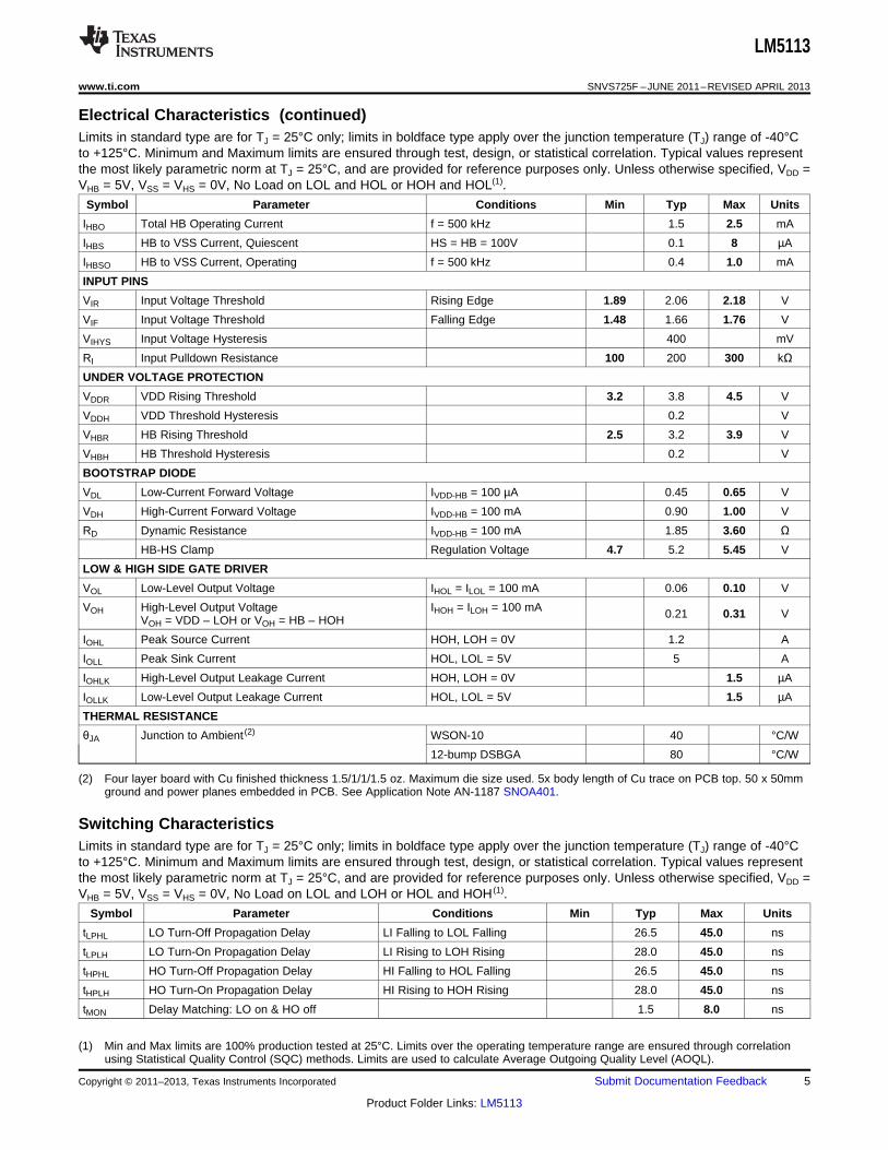
Switching CharacteristicsLimits in standard type are for TJ = 25°C only; limits in boldface type apply over the junction temperature (TJ) range of -40°Cto +125°C. Minimum and Maximum limits are ensured through test, design, or statistical correlation. Typical values representthe most likely parametric norm at TJ = 25°C, and are provided for reference purposes only. Unless otherwise specified, VDD =VHB = 5V, VSS = VHS = 0V, No Load on LOL and LOH or HOL and HOH (1).
Symbol Parameter Conditions Min Typ Max Units
tLPHL LO Turn-Off Propagation Delay LI Falling to LOL Falling 26.5 45.0 ns
tLPLH LO Turn-On Propagation Delay LI Rising to LOH Rising 28.0 45.0 ns
tHPHL HO Turn-Off Propagation Delay HI Falling to HOL Falling 26.5 45.0 ns
tHPLH HO Turn-On Propagation Delay HI Rising to HOH Rising 28.0 45.0 ns
tMON Delay Matching: LO on & HO off 1.5 8.0 ns
(1) Min and Max limits are 100% production tested at 25°C. Limits over the operating temperature range are ensured through correlationusing Statistical Quality Control (SQC) methods. Limits are used to calculate Average Outgoing Quality Level (AOQL).
Copyright © 2011–2013, Texas Instruments Incorporated Submit Documentation Feedback 5
Product Folder Links: LM5113
LI
HI
tHPLHtLPLH
tHPHLtLPHL
LO
HO
LI
HI
tMOFFtMON
LO
HO
LM5113
SNVS725F –JUNE 2011–REVISED APRIL 2013 www.ti.com
Switching Characteristics (continued)Limits in standard type are for TJ = 25°C only; limits in boldface type apply over the junction temperature (TJ) range of -40°Cto +125°C. Minimum and Maximum limits are ensured through test, design, or statistical correlation. Typical values representthe most likely parametric norm at TJ = 25°C, and are provided for reference purposes only. Unless otherwise specified, VDD =VHB = 5V, VSS = VHS = 0V, No Load on LOL and LOH or HOL and HOH(1).
Symbol Parameter Conditions Min Typ Max Units
tMOFF Delay Matching: LO off & HO on 1.5 8.0 ns
tHRC HO Rise Time (0.5V - 4.5V) CL = 1000 pF 7.0 ns
tLRC LO Rise Time (0.5V – 4.5V) CL = 1000 pF 7.0 ns
tHFC HO Fall Time (0.5V - 4.5V) CL = 1000 pF 1.5 ns
tLFC LO Fall Time (0.5V - 4.5V) CL = 1000 pF 1.5 ns
tPW Minimum Input Pulse Width that Changes 10 nsthe Output
tBS Bootstrap Diode Reverse Recovery Time IF = 100mA, 40 nsIR = 100mA
Timing Diagram
Figure 3. Timing Diagram
6 Submit Documentation Feedback Copyright © 2011–2013, Texas Instruments Incorporated
Product Folder Links: LM5113
LM5113
www.ti.com SNVS725F –JUNE 2011–REVISED APRIL 2013
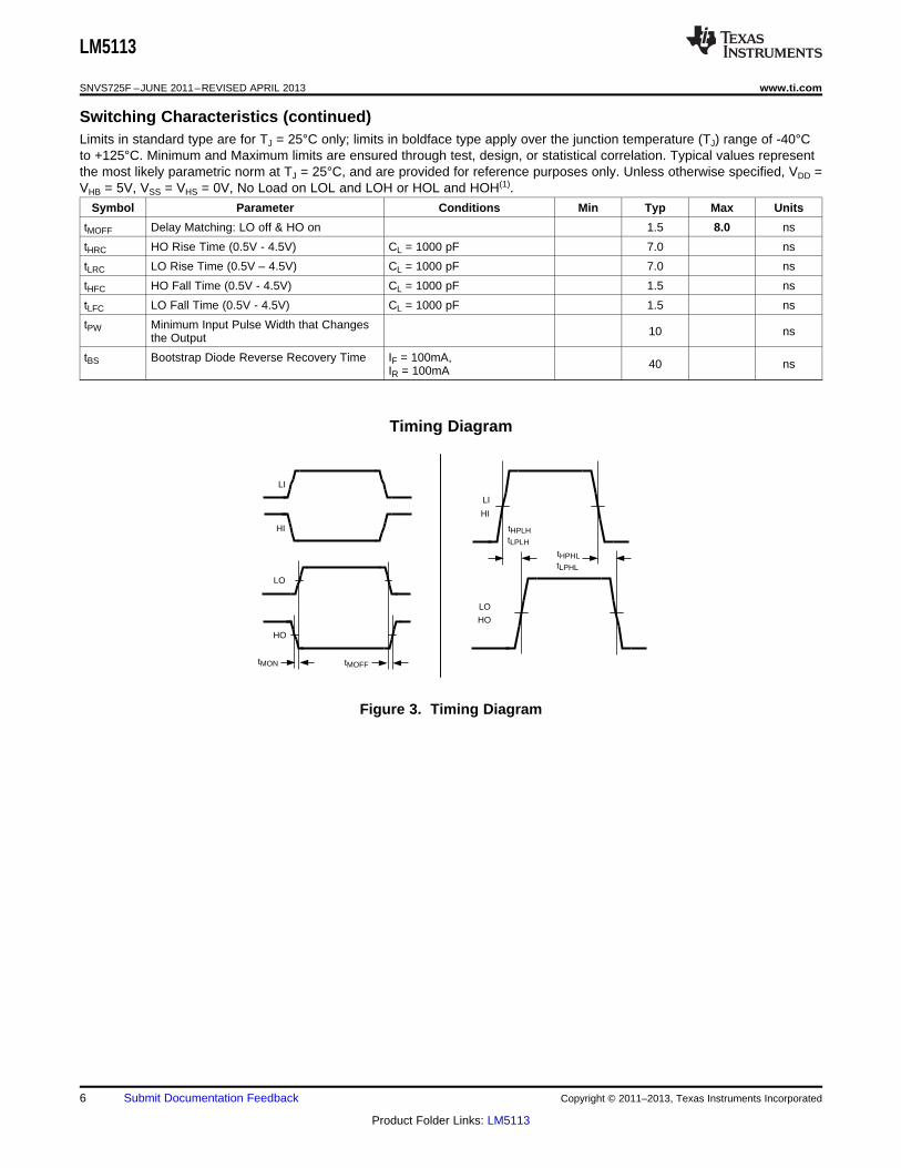
Typical Performance Characteristics
Peak Source Current Peak Sink Currentvs Output Voltage vs Output Voltage
Figure 4. Figure 5.
IDDO IHBOvs Frequency vs Frequency
Figure 6. Figure 7.
IDD IHBvs Temperature vs Temperature
Figure 8. Figure 9.
Copyright © 2011–2013, Texas Instruments Incorporated Submit Documentation Feedback 7
Product Folder Links: LM5113

LM5113
SNVS725F –JUNE 2011–REVISED APRIL 2013 www.ti.com
Typical Performance Characteristics (continued)UVLO Rising Thresholds UVLO Falling Thresholds
vs Temperature vs Temperature
Figure 10. Figure 11.
Input Thresholds Input Threshold Hysteresisvs Temperature vs Temperature
Figure 12. Figure 13.
Propagation DelayBootstrap Diode Forward Voltage vs Temperature
Figure 14. Figure 15.
8 Submit Documentation Feedback Copyright © 2011–2013, Texas Instruments Incorporated
Product Folder Links: LM5113
LM5113
www.ti.com SNVS725F –JUNE 2011–REVISED APRIL 2013
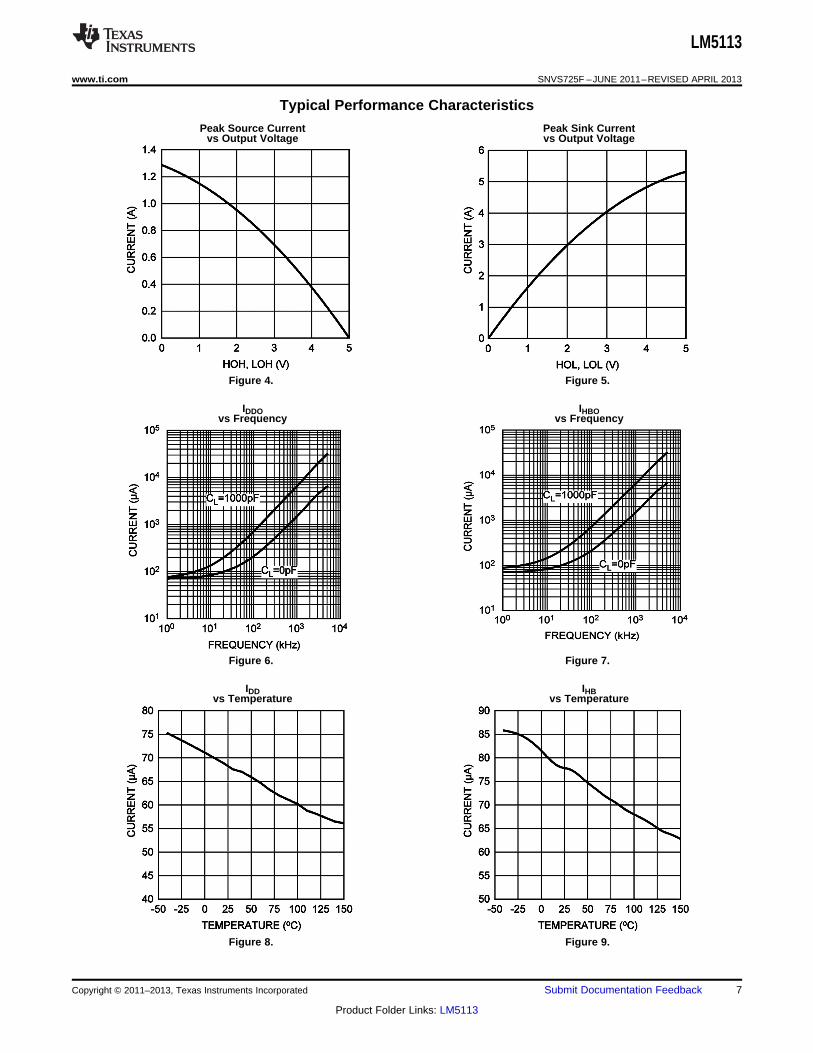
Typical Performance Characteristics (continued)LO&HO Gate Drive — High/Low Level Output Voltage HB Regulation Voltage
vs Temperature vs Temperature
Figure 16. Figure 17.
(1) Note Unless otherwise specified, VDD = VHB = 5V, VSS = VHS = 0V.
Copyright © 2011–2013, Texas Instruments Incorporated Submit Documentation Feedback 9
Product Folder Links: LM5113

LM5113
SNVS725F –JUNE 2011–REVISED APRIL 2013 www.ti.com
Detailed Operating Description
The LM5113 is designed to drive both the high-side and the low-side enhancement mode Gallium Nitride FETs ina synchronous buck or a half-bridge configuration. The outputs of the LM5113 are independently controlled withTTL input thresholds. The inputs of the LM5113 can withstand voltages up to 14V regardless of the VDD voltage,and can be directly connected to the outputs of PWM controllers.
The high side driver uses the floating bootstrap capacitor voltage to drive the high-side FET. As shown inFigure 1, the bootstrap capacitor is recharged through an internal bootstrap diode each cycle when the HS pin ispulled below the VDD voltage. For inductive load applications the HS node will fall to a negative potential,clamped by the low side FET.
Due to the intrinsic feature of enhancement mode GaN FETs the source-to-drain voltage, when the gate is pulledlow, is usually higher than a diode forward voltage drop. This can lead to an excessive bootstrap voltage that candamage the high-side GaN FET. The LM5113 solves this problem with an internal clamping circuit that preventsthe bootstrap voltage from exceeding 5.2V typical.
The output pull-down and pull-up resistance of LM5113 is optimized for enhancement mode GaN FETs toachieve high frequency, efficient operation. The 0.6Ω pull-down resistance provides a robust low impedance turn-off path necessary to eliminate undesired turn-on induced by high dv/dt or high di/dt. The 2.1Ω pull-up resistancehelps reduce the ringing and over-shoot of the switch node voltage. The split outputs of the LM5113 offerflexibility to adjust the turn-on and turn-off speed by independently adding additional impedance in either the turn-on path and/or the turn-off path.
The LM5113 has an Under-voltage Lockout (UVLO) on both the VDD and bootstrap supplies. When the VDDvoltage is below the threshold voltage of 3.8V, both the HI and LI inputs are ignored, to prevent the GaN FETsfrom being partially turned on. Also if there is sufficient VDD voltage, the UVLO will actively pull the LOL andHOL low. When the HB to HS bootstrap voltage is below the UVLO threshold of 3.2V, only HOL is pulled low.Both UVLO threshold voltages have 200mV of hysteresis to avoid chattering.
Bypass Capacitor
The VDD bypass capacitor provides the gate charge for the low-side and high-side transistors and to absorb thereverse recovery charge of the bootstrap diode. The required bypass capacitance can be calculated as follows:
(1)
QgH and QgL are gate charge of the high-side and low-side transistors respectively. Qrr is the reverse recoverycharge of the bootstrap diode, which is typically around 4nC. ΔV is the maximum allowable voltage drop acrossthe bypass capacitor. A 0.1uF or larger value, good quality, ceramic capacitor is recommended. The bypasscapacitor should be placed as close to the pins of the IC as possible to minimize the parasitic inductance.
Bootstrap Capacitor
The bootstrap capacitor provides the gate charge for the high-side switch, dc bias power for HB under-voltagelockout circuit, and the reverse recovery charge of the bootstrap diode. The required bypass capacitance can becalculated as follows:
(2)
IHB is the quiescent current of the high-side driver. ton is the maximum on-time period of the high-side transistor.A good quality, ceramic capacitor should be used for the bootstrap capacitor. It is recommended to place thebootstrap capacitor as close to the HB and HS pins as possible.
Power Dissipation
The power consumption of the driver is an important measure that determines the maximum achievableoperating frequency of the driver. It should be kept below the maximum power dissipation limit of the package atthe operating temperature. The total power dissipation of the LM5113 is the sum of the gate driver losses and thebootstrap diode power loss.
The gate driver losses are incurred by charge and discharge of the capacitive load. It can be approximated as
10 Submit Documentation Feedback Copyright © 2011–2013, Texas Instruments Incorporated
Product Folder Links: LM5113
LM5113
www.ti.com SNVS725F –JUNE 2011–REVISED APRIL 2013
(3)
CLoadH and CLoadL are the high-side and the low-side capacitive loads respectively. It can also be calculated withthe total input gate charge of the high-side and the low-side transistors as
(4)
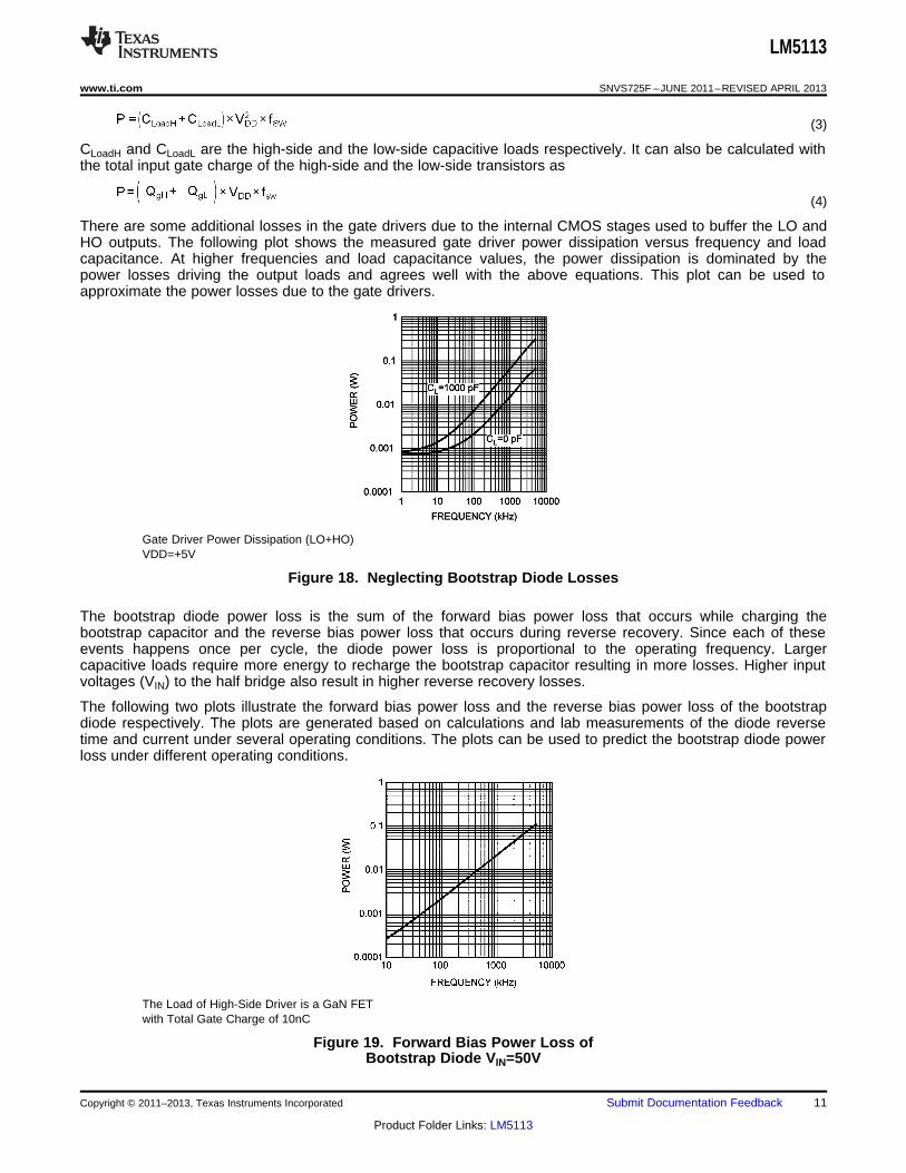
There are some additional losses in the gate drivers due to the internal CMOS stages used to buffer the LO andHO outputs. The following plot shows the measured gate driver power dissipation versus frequency and loadcapacitance. At higher frequencies and load capacitance values, the power dissipation is dominated by thepower losses driving the output loads and agrees well with the above equations. This plot can be used toapproximate the power losses due to the gate drivers.
Gate Driver Power Dissipation (LO+HO)VDD=+5V
Figure 18. Neglecting Bootstrap Diode Losses
The bootstrap diode power loss is the sum of the forward bias power loss that occurs while charging thebootstrap capacitor and the reverse bias power loss that occurs during reverse recovery. Since each of theseevents happens once per cycle, the diode power loss is proportional to the operating frequency. Largercapacitive loads require more energy to recharge the bootstrap capacitor resulting in more losses. Higher inputvoltages (VIN) to the half bridge also result in higher reverse recovery losses.
The following two plots illustrate the forward bias power loss and the reverse bias power loss of the bootstrapdiode respectively. The plots are generated based on calculations and lab measurements of the diode reversetime and current under several operating conditions. The plots can be used to predict the bootstrap diode powerloss under different operating conditions.
The Load of High-Side Driver is a GaN FETwith Total Gate Charge of 10nC
Figure 19. Forward Bias Power Loss ofBootstrap Diode VIN=50V
Copyright © 2011–2013, Texas Instruments Incorporated Submit Documentation Feedback 11
Product Folder Links: LM5113

(TJ - TA)TJA
P =
LM5113
SNVS725F –JUNE 2011–REVISED APRIL 2013 www.ti.com
The Load of High-Side Driver is a GaN FETwith Total Gate Charge of 10nC
Figure 20. Reverse Recovery Power Loss ofBootstrap Diode VIN=50V
The sum of the driver loss and the bootstrap diode loss is the total power loss of the IC. For a given ambienttemperature, the maximum allowable power loss of the IC can be defined as
(5)
Layout Considerations
Small gate capacitance and miller capacitance enable enhancement mode GaN FETs to operate with fastswitching speed. The induced high dv/dt and di/dt, coupled with a low gate threshold voltage and limitedheadroom of enhancement mode GaN FETs gate voltage, make the circuit layout crucial to the optimumperformance. Following are some hints.1. The first priority in designing the layout of the driver is to confine the high peak currents that charge and
discharge the GaN FETs gate into a minimal physical area. This will decrease the loop inductance andminimize noise issues on the gate terminal of the GaN FETs. The GaN FETs should be placed close to thedriver.
2. The second high current path includes the bootstrap capacitor, the local ground referenced VDD bypasscapacitor and low-side GaN FET. The bootstrap capacitor is recharged on a cycle-by-cycle basis through thebootstrap diode from the ground referenced VDD capacitor. The recharging occurs in a short time intervaland involves high peak current. Minimizing this loop length and area on the circuit board is important toensure reliable operation.
3. The parasitic inductance in series with the source of the high-side FET and the low-side FET can imposeexcessive negative voltage transients on the driver. It is recommended to connect HS pin and VSS pin to therespective source of the high-side and low-side transistors with a short and low-inductance path.
4. The parasitic source inductance, along with the gate capacitor and the driver pull-down path, can form a LCRresonant tank, resulting in gate voltage oscillations. An optional resistor or ferrite bead can be used to dampthe ringing.
5. Low ESR/ESL capacitors must be connected close to the IC, between VDD and VSS pins and between theHB and HS pins to support the high peak current being drawn from VDD during turn-on of the FETs. It ismost desirable to place the VDD decoupling capacitor and the HB to HS bootstrap capacitor on the sameside of the PC board as the driver. The inductance of vias can impose excessive ringing on the IC pins.
6. To prevent excessive ringing on the input power bus, good decoupling practices are required by placing lowESR ceramic capacitors adjacent to the GaN FETs.
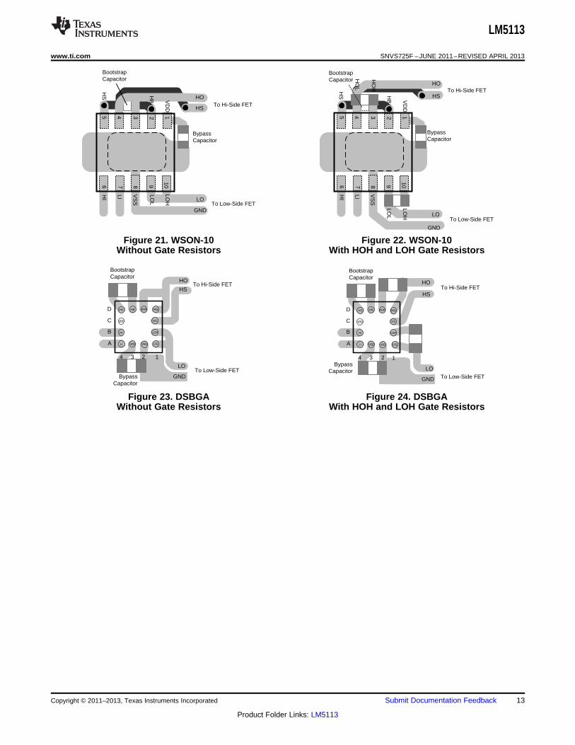
The following figures show recommended layout patterns for WSON-10 package and DSBGA packagerespectively. Two cases are considered: (1) Without any gate resistors; (2) With an optional turn-on gate resistor.It should be noted that 0402 DSBGA package is assumed for the passive components in the drawings. Forinformation on DSBGA package assembly, refer to Application Note AN-1112 SNVA009.
12 Submit Documentation Feedback Copyright © 2011–2013, Texas Instruments Incorporated
Product Folder Links: LM5113
A
B
C
D
1
To Hi-Side FETHO
To Low-Side FETLO
GNDBypass Capacitor
Bootstrap Capacitor
34
HS
2
VDDLI
HI
VDD
HS HB HOH HOL
LOH
LOLVSS
HS
A
B
C
D
12
To Hi-Side FETHO
To Low-Side FETLO
GND
Bypass Capacitor
Bootstrap Capacitor
HS
34
VDDLI
HI
VDD
HS HB HOH HOL
LOH
LOLVSS
HS
To Low-Side FET
HI
LI
VS
S
LOH
LOL
9 10
To Hi-Side FET
LO
GND
HS
6 7 8
125
VD
D
HB
Bypass Capacitor
4
HS
Bootstrap Capacitor
HO
HO
H
HO
L
3To Low-Side FET
HI
LI
VS
S
LOH
LOL
9 10
To Hi-Side FET
LO
GND
HO
HS
6 7 8
12345
VD
D
HB
Bootstrap Capacitor
Bypass Capacitor
HS
LM5113
www.ti.com SNVS725F –JUNE 2011–REVISED APRIL 2013
Figure 21. WSON-10 Figure 22. WSON-10Without Gate Resistors With HOH and LOH Gate Resistors
Figure 23. DSBGA Figure 24. DSBGAWithout Gate Resistors With HOH and LOH Gate Resistors
Copyright © 2011–2013, Texas Instruments Incorporated Submit Documentation Feedback 13
Product Folder Links: LM5113
LM5113
SNVS725F –JUNE 2011–REVISED APRIL 2013 www.ti.com
REVISION HISTORY
Changes from Revision E (April 2013) to Revision F Page
• Changed layout of National Data Sheet to TI format .......................................................................................................... 13
14 Submit Documentation Feedback Copyright © 2011–2013, Texas Instruments Incorporated
Product Folder Links: LM5113
PACKAGE OPTION ADDENDUM
www.ti.com 10-Dec-2020
Addendum-Page 1
PACKAGING INFORMATION
Orderable Device Status(1)
Package Type PackageDrawing
Pins PackageQty
Eco Plan(2)
Lead finish/Ball material
(6)
MSL Peak Temp(3)
Op Temp (°C) Device Marking(4/5)
Samples
LM5113SD/NOPB NRND WSON DPR 10 1000 RoHS & Green SN Level-1-260C-UNLIM -40 to 125 L5113
LM5113SDE/NOPB NRND WSON DPR 10 250 RoHS & Green SN Level-1-260C-UNLIM -40 to 125 L5113
LM5113SDX/NOPB NRND WSON DPR 10 4500 RoHS & Green SN Level-1-260C-UNLIM -40 to 125 L5113
LM5113TME/NOPB NRND DSBGA YFX 12 250 RoHS & Green SNAGCU Level-1-260C-UNLIM 5113
LM5113TMX/NOPB NRND DSBGA YFX 12 3000 RoHS & Green SNAGCU Level-1-260C-UNLIM 5113 (1) The marketing status values are defined as follows:ACTIVE: Product device recommended for new designs.LIFEBUY: TI has announced that the device will be discontinued, and a lifetime-buy period is in effect.NRND: Not recommended for new designs. Device is in production to support existing customers, but TI does not recommend using this part in a new design.PREVIEW: Device has been announced but is not in production. Samples may or may not be available.OBSOLETE: TI has discontinued the production of the device.
(2) RoHS: TI defines "RoHS" to mean semiconductor products that are compliant with the current EU RoHS requirements for all 10 RoHS substances, including the requirement that RoHS substancedo not exceed 0.1% by weight in homogeneous materials. Where designed to be soldered at high temperatures, "RoHS" products are suitable for use in specified lead-free processes. TI mayreference these types of products as "Pb-Free".RoHS Exempt: TI defines "RoHS Exempt" to mean products that contain lead but are compliant with EU RoHS pursuant to a specific EU RoHS exemption.Green: TI defines "Green" to mean the content of Chlorine (Cl) and Bromine (Br) based flame retardants meet JS709B low halogen requirements of <=1000ppm threshold. Antimony trioxide basedflame retardants must also meet the <=1000ppm threshold requirement.
(3) MSL, Peak Temp. - The Moisture Sensitivity Level rating according to the JEDEC industry standard classifications, and peak solder temperature.
(4) There may be additional marking, which relates to the logo, the lot trace code information, or the environmental category on the device.
(5) Multiple Device Markings will be inside parentheses. Only one Device Marking contained in parentheses and separated by a "~" will appear on a device. If a line is indented then it is a continuationof the previous line and the two combined represent the entire Device Marking for that device.
(6) Lead finish/Ball material - Orderable Devices may have multiple material finish options. Finish options are separated by a vertical ruled line. Lead finish/Ball material values may wrap to twolines if the finish value exceeds the maximum column width.
Important Information and Disclaimer:The information provided on this page represents TI's knowledge and belief as of the date that it is provided. TI bases its knowledge and belief on informationprovided by third parties, and makes no representation or warranty as to the accuracy of such information. Efforts are underway to better integrate information from third parties. TI has taken andcontinues to take reasonable steps to provide representative and accurate information but may not have conducted destructive testing or chemical analysis on incoming materials and chemicals.TI and TI suppliers consider certain information to be proprietary, and thus CAS numbers and other limited information may not be available for release.
PACKAGE OPTION ADDENDUM
www.ti.com 10-Dec-2020
Addendum-Page 2
In no event shall TI's liability arising out of such information exceed the total purchase price of the TI part(s) at issue in this document sold by TI to Customer on an annual basis.
OTHER QUALIFIED VERSIONS OF LM5113 :
• Automotive: LM5113-Q1
NOTE: Qualified Version Definitions:
• Automotive - Q100 devices qualified for high-reliability automotive applications targeting zero defects

TAPE AND REEL INFORMATION
*All dimensions are nominal
Device PackageType
PackageDrawing
Pins SPQ ReelDiameter
(mm)
ReelWidth
W1 (mm)
A0(mm)
B0(mm)
K0(mm)
P1(mm)
W(mm)
Pin1Quadrant
LM5113SD/NOPB WSON DPR 10 1000 178.0 12.4 4.3 4.3 1.3 8.0 12.0 Q1
LM5113SDE/NOPB WSON DPR 10 250 178.0 12.4 4.3 4.3 1.3 8.0 12.0 Q1
LM5113SDX/NOPB WSON DPR 10 4500 330.0 12.4 4.3 4.3 1.3 8.0 12.0 Q1
LM5113TME/NOPB DSBGA YFX 12 250 178.0 8.4 1.85 2.01 0.76 4.0 8.0 Q1
LM5113TMX/NOPB DSBGA YFX 12 3000 178.0 8.4 1.85 2.01 0.76 4.0 8.0 Q1
PACKAGE MATERIALS INFORMATION
www.ti.com 21-Oct-2021
Pack Materials-Page 1
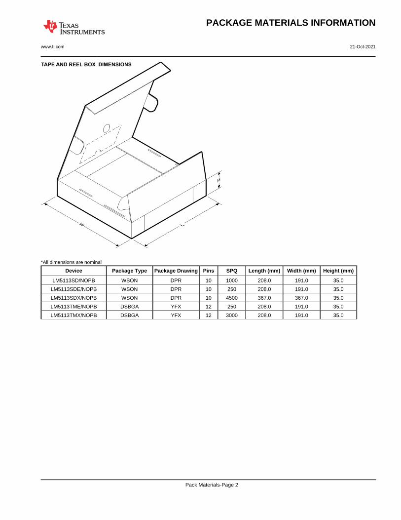
*All dimensions are nominal
Device Package Type Package Drawing Pins SPQ Length (mm) Width (mm) Height (mm)
LM5113SD/NOPB WSON DPR 10 1000 208.0 191.0 35.0
LM5113SDE/NOPB WSON DPR 10 250 208.0 191.0 35.0
LM5113SDX/NOPB WSON DPR 10 4500 367.0 367.0 35.0
LM5113TME/NOPB DSBGA YFX 12 250 208.0 191.0 35.0
LM5113TMX/NOPB DSBGA YFX 12 3000 208.0 191.0 35.0
PACKAGE MATERIALS INFORMATION
www.ti.com 21-Oct-2021
Pack Materials-Page 2
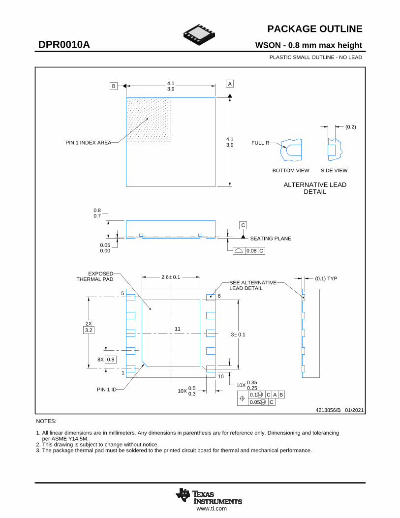
www.ti.com
PACKAGE OUTLINE
C
10X 0.350.25
3 0.1
2.6 0.1
0.80.7
8X 0.8
10X 0.50.3
(0.1) TYP
2X3.2
0.050.00
B 4.13.9
A
4.13.9
(0.2)
WSON - 0.8 mm max heightDPR0010APLASTIC SMALL OUTLINE - NO LEAD
4218856/B 01/2021
PIN 1 INDEX AREA
SEATING PLANE
0.08 C
1
5 6
10
PIN 1 ID0.1 C A B0.05 C
THERMAL PADEXPOSED
SEE ALTERNATIVELEAD DETAIL
11
NOTES: 1. All linear dimensions are in millimeters. Any dimensions in parenthesis are for reference only. Dimensioning and tolerancing per ASME Y14.5M. 2. This drawing is subject to change without notice. 3. The package thermal pad must be soldered to the printed circuit board for thermal and mechanical performance.
SCALE 3.000
20.000
FULL R
ALTERNATIVE LEADDETAIL
BOTTOM VIEW SIDE VIEW
www.ti.com
EXAMPLE BOARD LAYOUT
(R0.05) TYP
8X (0.8)
0.07 MINALL AROUND0.07 MAX
ALL AROUND
(2.6)
(3.8)
10X (0.3)
10X (0.6)
(3)
( 0.2) VIATYP
(1.25)
(1.05)
WSON - 0.8 mm max heightDPR0010APLASTIC SMALL OUTLINE - NO LEAD
4218856/B 01/2021
SYMM
1
56
10
SYMM
LAND PATTERN EXAMPLEEXPOSED METAL SHOWN
SCALE:15X
11
NOTES: (continued) 4. This package is designed to be soldered to a thermal pad on the board. For more information, see Texas Instruments literature number SLUA271 (www.ti.com/lit/slua271).
SOLDER MASKOPENINGSOLDER MASK
METAL UNDER
SOLDER MASKDEFINED
EXPOSEDMETAL
METALEDGE
SOLDER MASKOPENING
SOLDER MASK DETAILS
NON SOLDER MASKDEFINED
(PREFERRED)
EXPOSEDMETAL
www.ti.com
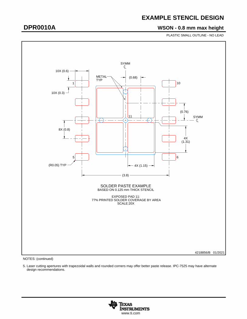
EXAMPLE STENCIL DESIGN
10X (0.3)
10X (0.6)
8X (0.8)
4X(1.31)
4X (1.15)
(0.76)
(3.8)
(R0.05) TYP
(0.68)
WSON - 0.8 mm max heightDPR0010APLASTIC SMALL OUTLINE - NO LEAD
4218856/B 01/2021
NOTES: (continued) 5. Laser cutting apertures with trapezoidal walls and rounded corners may offer better paste release. IPC-7525 may have alternate design recommendations.
SOLDER PASTE EXAMPLEBASED ON 0.125 mm THICK STENCIL
EXPOSED PAD 11:
77% PRINTED SOLDER COVERAGE BY AREASCALE:20X
SYMM
1
5 6
10
SYMM
METALTYP
11
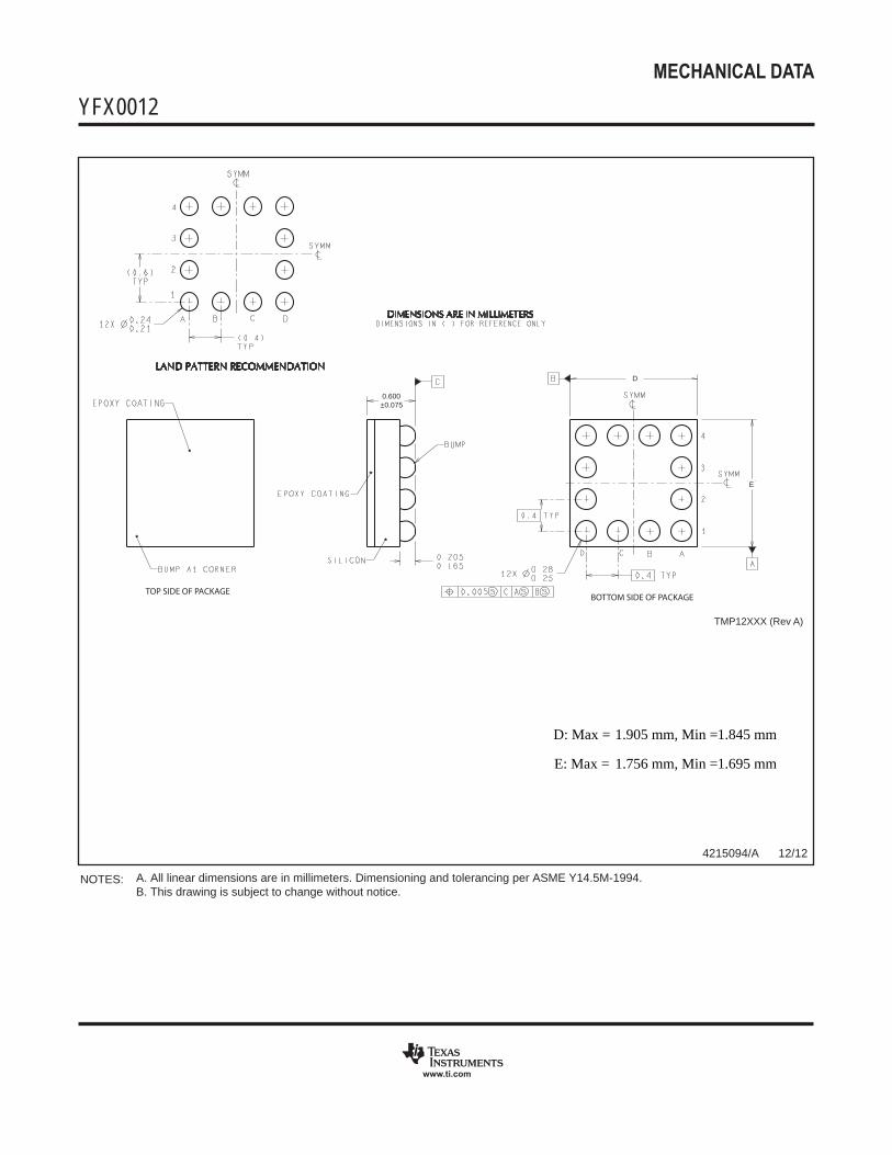
MECHANICAL DATA
YFX0012xxx
www.ti.com
TMP12XXX (Rev A)
TOP SIDE OF PACKAGEBOTTOM SIDE OF PACKAGE
A. All linear dimensions are in millimeters. Dimensioning and tolerancing per ASME Y14.5M-1994.B. This drawing is subject to change without notice.
NOTES:
4215094/A 12/12
0.600±0.075
D
E
D: Max =
E: Max =
1.905 mm, Min =
1.756 mm, Min =
1.845 mm
1.695 mm

IMPORTANT NOTICE AND DISCLAIMERTI PROVIDES TECHNICAL AND RELIABILITY DATA (INCLUDING DATA SHEETS), DESIGN RESOURCES (INCLUDING REFERENCE DESIGNS), APPLICATION OR OTHER DESIGN ADVICE, WEB TOOLS, SAFETY INFORMATION, AND OTHER RESOURCES “AS IS” AND WITH ALL FAULTS, AND DISCLAIMS ALL WARRANTIES, EXPRESS AND IMPLIED, INCLUDING WITHOUT LIMITATION ANY IMPLIED WARRANTIES OF MERCHANTABILITY, FITNESS FOR A PARTICULAR PURPOSE OR NON-INFRINGEMENT OF THIRD PARTY INTELLECTUAL PROPERTY RIGHTS.These resources are intended for skilled developers designing with TI products. You are solely responsible for (1) selecting the appropriate TI products for your application, (2) designing, validating and testing your application, and (3) ensuring your application meets applicable standards, and any other safety, security, regulatory or other requirements.These resources are subject to change without notice. TI grants you permission to use these resources only for development of an application that uses the TI products described in the resource. Other reproduction and display of these resources is prohibited. No license is granted to any other TI intellectual property right or to any third party intellectual property right. TI disclaims responsibility for, and you will fully indemnify TI and its representatives against, any claims, damages, costs, losses, and liabilities arising out of your use of these resources.TI’s products are provided subject to TI’s Terms of Sale or other applicable terms available either on ti.com or provided in conjunction with such TI products. TI’s provision of these resources does not expand or otherwise alter TI’s applicable warranties or warranty disclaimers for TI products.TI objects to and rejects any additional or different terms you may have proposed. IMPORTANT NOTICE
Mailing Address: Texas Instruments, Post Office Box 655303, Dallas, Texas 75265Copyright © 2021, Texas Instruments Incorporated


![Application Brochure A265 - Patriot Supply1].pdf · Electrical Essential Control Settings ... 115 V (ac) Class II Transformer L Do not apply power 12 13 Com – 5A 5A 5A 5A 5A 5A](https://static.fdocuments.in/doc/165x107/5eaeca02e603423ba506622e/application-brochure-a265-patriot-1pdf-electrical-essential-control-settings.jpg)