100V N-Channel MOSFET
5
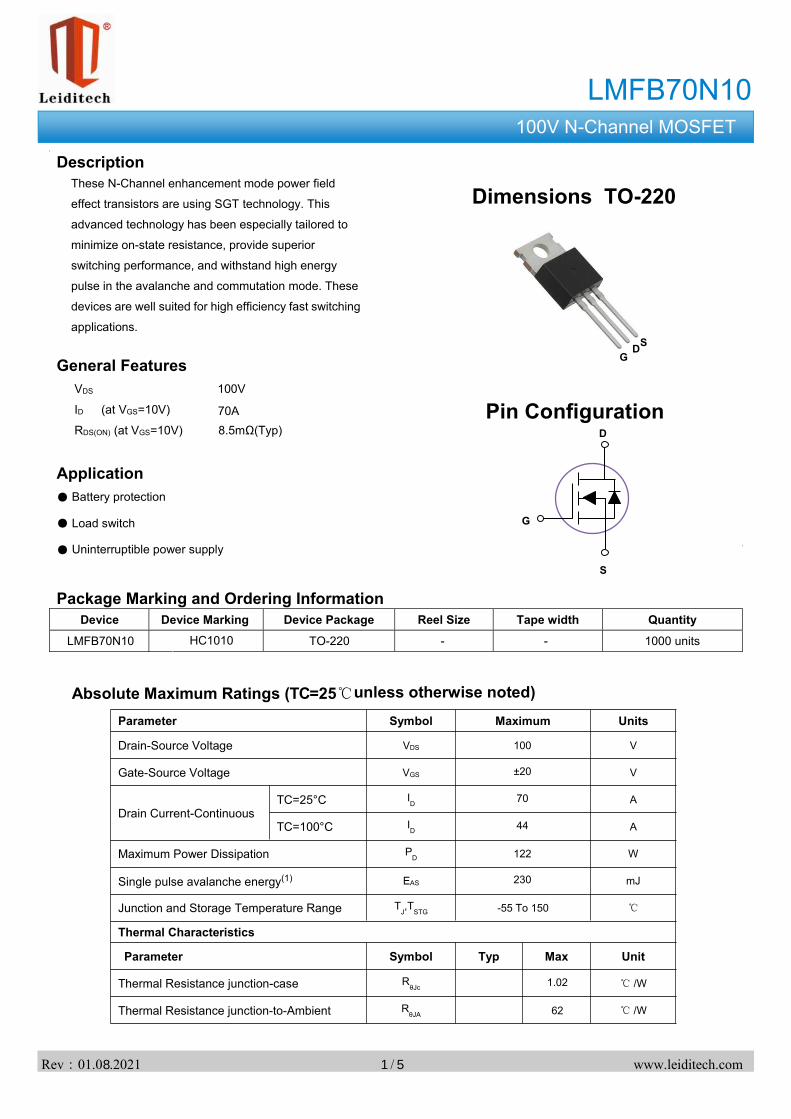
LMFB70N10 100V N-Channel MOSFET Description General Features Application ● ● Package Marking and Ordering Information Device Marking Device Device Package Reel Size Tape width Quantity HC1010 LMFB70N10 TO-220 1000 units Dimensions TO-220 Pin Configuration www.leiditech.com Absolute Maximum Ratings (TC=25℃ unless otherwise noted) - - Rev : 01.0 .2021 / 15 8 G D S Battery protection Load switch Uninterruptible power supply ● D G S These N-Channel enhancement mode power field effect transistors are using SGT technology. This advanced technology has been especially tailored to minimize on-state resistance, provide superior switching performance, and withstand high energy pulse in the avalanche and commutation mode. These devices are well suited for high efficiency fast switching applications. VDS 100V ID (at VGS=10V) 70A RDS(ON) (at VGS=10V) 8.5mΩ(Typ) Parameter Symbol Maximum Units Drain-Source Voltage VDS 100 V Gate-Source Voltage VGS ±20 V Drain Current-Continuous TC=25°C I D 70 A TC=100°C I D 44 A Maximum Power Dissipation P D 122 W Single pulse avalanche energy (1) EAS 230 mJ Junction and Storage Temperature Range T J ,T STG -55 To 150 ℃ Thermal Characteristics Parameter Symbol Typ Max Unit Thermal Resistance junction-case R θJc 1.02 ℃ /W Thermal Resistance junction-to-Ambient R θJA 62 ℃ /W
Transcript of 100V N-Channel MOSFET
LMFB70N10100V N-Channel MOSFET
Description
General Features
Application
Package Marking and Ordering Information Device Marking Device Device Package Reel Size Tape width Quantity
HC1010LMFB70N10 TO-220 1000 units
Dimensions TO-220
Pin Configuration
www.leiditech.com
Absolute Maximum Ratings (TC=25unless otherwise noted)
- -
Rev : 01.0 .2021 /1 58
G D S
Battery protection
Load switch
Uninterruptible power supply
D
G
S
These N-Channel enhancement mode power field
effect transistors are using SGT technology. This
advanced technology has been especially tailored to
minimize on-state resistance, provide superior
switching performance, and withstand high energy
pulse in the avalanche and commutation mode. These
devices are well suited for high efficiency fast switching
applications.
VDS 100V
ID (at VGS=10V) 70ARDS(ON) (at VGS=10V) 8.5mΩ(Typ)
Parameter Symbol Maximum Units
Drain-Source Voltage VDS 100 V
Gate-Source Voltage VGS ±20 V
Drain Current-ContinuousTC=25°C I
D 70 A
TC=100°C ID 44 A
Maximum Power Dissipation PD 122 W
Single pulse avalanche energy(1) EAS 230 mJ
Junction and Storage Temperature Range TJ,T
STG -55 To 150
Thermal Characteristics
Parameter Symbol Typ Max Unit
Thermal Resistance junction-case RθJc 1.02 /W
Thermal Resistance junction-to-Ambient RθJA 62 /W
www.leiditech.com
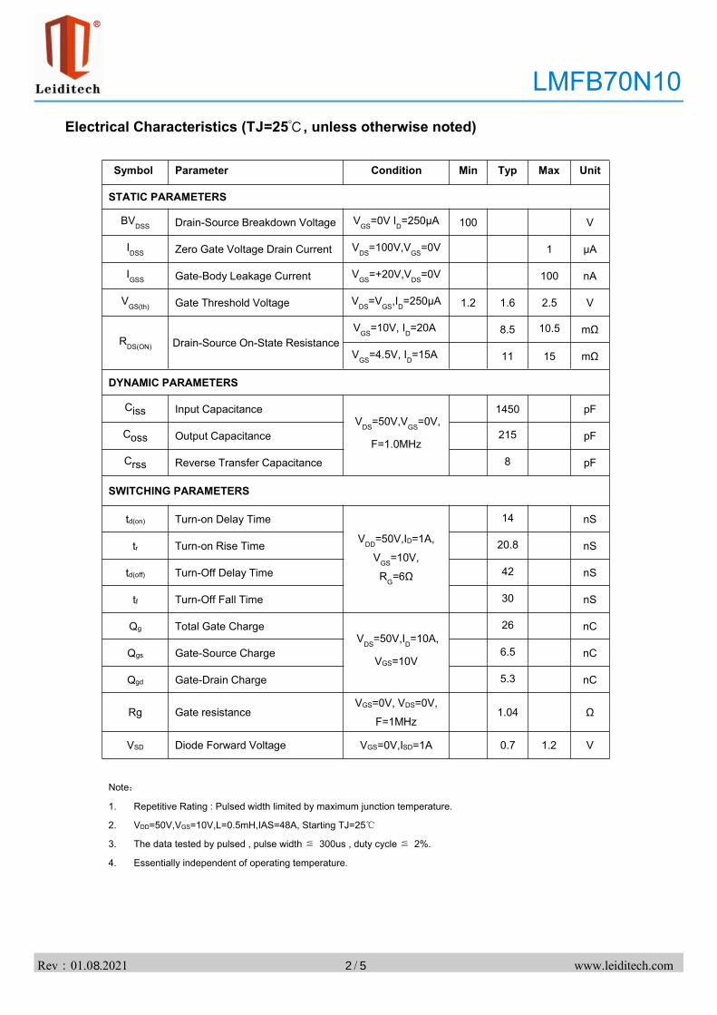
Electrical Characteristics (TJ=25 , unless otherwise noted)
Rev : 01.0 .2021 /2 58
Symbol Parameter Condition Min Typ Max Unit
STATIC PARAMETERS
BVDSS Drain-Source Breakdown Voltage VGS=0V ID=250μA 100 V
IDSS Zero Gate Voltage Drain Current VDS=100V,VGS=0V 1 μA
IGSS Gate-Body Leakage Current VGS=+20V,VDS=0V 100 nA
VGS(th) Gate Threshold Voltage VDS=VGS,ID=250μA 1.2 1.6 2.5 V
RDS(ON) Drain-Source On-State ResistanceVGS=10V, ID=20A 8.5 10.5 mΩ
VGS=4.5V, ID=15A 11 15 mΩ
DYNAMIC PARAMETERS
Ciss Input CapacitanceVDS=50V,VGS=0V,
F=1.0MHz
1450 pF
Coss Output Capacitance 215 pF
Crss Reverse Transfer Capacitance 8 pF
SWITCHING PARAMETERS
td(on) Turn-on Delay Time
VDD=50V,ID=1A,
VGS=10V,
RG=6Ω
14 nS
tr Turn-on Rise Time 20.8 nS
td(off) Turn-Off Delay Time 42 nS
tf Turn-Off Fall Time 30 nS
Qg Total Gate ChargeVDS=50V,ID=10A,
VGS=10V
26 nC
Qgs Gate-Source Charge 6.5 nC
Qgd Gate-Drain Charge 5.3 nC
Rg Gate resistanceVGS=0V, VDS=0V,
F=1MHz1.04 Ω
VSD Diode Forward Voltage VGS=0V,ISD=1A 0.7 1.2 V
Note:
1. Repetitive Rating : Pulsed width limited by maximum junction temperature.
2. VDD=50V,VGS=10V,L=0.5mH,IAS=48A, Starting TJ=25
3. The data tested by pulsed , pulse width ≦ 300us , duty cycle ≦ 2%.
4. Essentially independent of operating temperature.
LMFB70N10
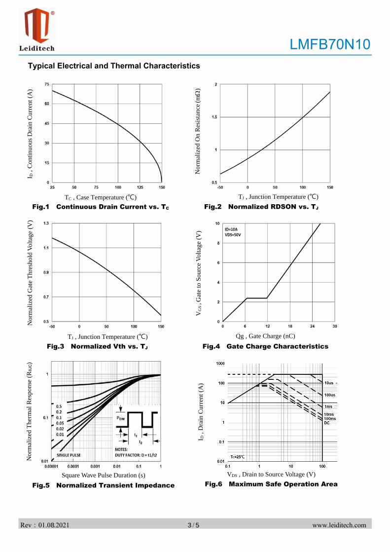
Typical Electrical and Thermal Characteristics
www.leiditech.comRev : 01.0 .2021 /3 58
I D ,
Co
nti
nu
ou
s D
rain
Cu
rren
t (A
)
TC , Case Temperature ()
Fig.1 Continuous Drain Current vs. TC
TJ , Junction Temperature ()
Fig.2 Normalized RDSON vs. TJ
No
rmal
ized
On
Res
ista
nce
(m
)
TJ , Junction Temperature ()
Fig.3 Normalized Vth vs. TJ
No
rmal
ized
Gat
e T
hre
sho
ld V
olt
age (
V)
Qg , Gate Charge (nC)
Fig.4 Gate Charge Characteristics
VG
S ,
Gat
e to
So
urc
e V
olt
age
(V)
Square Wave Pulse Duration (s)
Fig.5 Normalized Transient Impedance
VDS , Drain to Source Voltage (V)
Fig.6 Maximum Safe Operation Area
No
rmal
ized
Th
erm
al R
esp
on
se (
RθJ
C)
I D ,
Dra
in C
urr
ent
(A)
LMFB70N10
www.leiditech.comRev : 01.0 .2021 /4 58
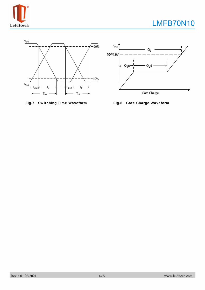
Td(on) Tr
Ton
Td(off) Tf
Toff
VDS
VGS
90%
10%
Fig.7 Switching Time Waveform Fig.8 Gate Charge Waveform
LMFB70N10
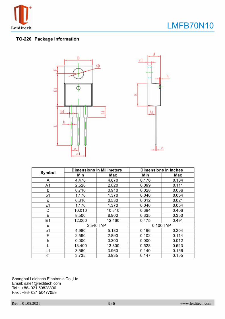
TO-220 Package Information
Shanghai Leiditech Electronic Co.,Ltd Email: [email protected] Tel : +86- 021 50828806 Fax : +86- 021 50477059
www.leiditech.comRev : 01.0 .2021 /5 58
Min Max Min MaxA 4.470 4.670 0.176 0.184
A1 2.520 2.820 0.099 0.111b 0.710 0.910 0.028 0.036
b1 1.170 1.370 0.046 0.054c 0.310 0.530 0.012 0.021c1 1.170 1.370 0.046 0.054D 10.010 10.310 0.394 0.406E 8.500 8.900 0.335 0.350
E1 12.060 12.460 0.475 0.491e
e1 4.980 5.180 0.196 0.204F 2.590 2.890 0.102 0.114h 0.000 0.300 0.000 0.012L 13.400 13.800 0.528 0.543
L1 3.560 3.960 0.140 0.156Φ 3.735 3.935 0.147 0.155
Symbol Dimensions In Millimeters Dimensions In Inches
0.100 TYP2.540 TYP
LMFB70N10