LM3722/LM3723/LM3724 5-PinMicroprocessor Reset … · LM3722, LM3723, LM3724 SNVS154E – MAY...
24
GND VCC PP LM3724 PUSHBUTTON SWITCH RESET INPUT MR VCC GND VCC RESET RL GND VCC PP LM3722 LM3723 PUSHBUTTON SWITCH RESET INPUT *(RESET) RESET MR VCC GND VCC LM3722, LM3723, LM3724 www.ti.com SNVS154E – MAY 2001 – REVISED MARCH 2013 LM3722/LM3723/LM3724 5-Pin Microprocessor Reset Circuits Check for Samples: LM3722, LM3723, LM3724 1FEATURES DESCRIPTION The LM3722/LM3723/LM3724 microprocessor 2• Precise Monitoring of 2.5V, 3.3V, and 5V supervisory circuits monitor the power supplies in Supply Voltages microprocessor and digital systems. They provide a • Fully Specified Over Temperature reset to the microprocessor during power-up, power- – Industrial: −40°C to +85°C down, brown-out conditions, and manual reset. – Extended: −40°C to +125°C The LM3722/LM3723/LM3724 asserts a reset signal whenever the supply decreases below the factory- • 100 ms Minimum Power-On Reset pulse Width, programmed reset threshold. Reset will be asserted 190 ms Typical: for at least 100ms even after V CC rises above the – Active-Low RESET Output (LM3722) reset threshold. – Active-High RESET Output (LM3723) The LM3722 has an active-low RESET push-pull – Active-Low RESET Open Drain Output output. The LM3723 has an active-high RESET push- (LM3724) pull output. The LM3724 has an active-low open-drain • Guaranteed RESET Output Valid for V CC ≥ 1V RESET output. • Low Supply Current, 6μA Typical Three standard reset voltage options are available, • Power Supply Transient Immunity suitable for monitoring 5V, 3.3V, and 2.5V supply voltages. Additional reset voltages are also available; • Compatible with MAX811/812 Applications contact Texas Instruments for details. APPLICATIONS With a low supply current of only 6μA, the LM3722/LM3723/LM3724 are ideal for use in portable • Microprocessor Systems equipment. The LM3722/LM3723/LM3724 are • Computers available in the 5-pin SOT-23 package. • Controllers • Intelligent Instruments • Portable/Battery-Powered Equipment Typical Application Circuits Figure 1. Typical Application Circuit Figure 2. Typical Application Circuit with R L Connection 1 Please be aware that an important notice concerning availability, standard warranty, and use in critical applications of Texas Instruments semiconductor products and disclaimers thereto appears at the end of this data sheet. 2All trademarks are the property of their respective owners. PRODUCTION DATA information is current as of publication date. Copyright © 2001–2013, Texas Instruments Incorporated Products conform to specifications per the terms of the Texas Instruments standard warranty. Production processing does not necessarily include testing of all parameters.
Transcript of LM3722/LM3723/LM3724 5-PinMicroprocessor Reset … · LM3722, LM3723, LM3724 SNVS154E – MAY...

GND
VCC
PPLM3724
PUSHBUTTON
SWITCH
RESET
INPUTMR
VCC
GND
VCC
RESET
RL
GND
VCC
PPLM3722
LM3723
PUSHBUTTON
SWITCH
RESET
INPUT*(RESET)RESET
MR
VCC
GND
VCC
LM3722, LM3723, LM3724
www.ti.com SNVS154E –MAY 2001–REVISED MARCH 2013
LM3722/LM3723/LM3724 5-Pin Microprocessor Reset CircuitsCheck for Samples: LM3722, LM3723, LM3724
1FEATURES DESCRIPTIONThe LM3722/LM3723/LM3724 microprocessor
2• Precise Monitoring of 2.5V, 3.3V, and 5Vsupervisory circuits monitor the power supplies inSupply Voltagesmicroprocessor and digital systems. They provide a
• Fully Specified Over Temperature reset to the microprocessor during power-up, power-– Industrial: −40°C to +85°C down, brown-out conditions, and manual reset.– Extended: −40°C to +125°C The LM3722/LM3723/LM3724 asserts a reset signal
whenever the supply decreases below the factory-• 100 ms Minimum Power-On Reset pulse Width,programmed reset threshold. Reset will be asserted190 ms Typical:for at least 100ms even after VCC rises above the– Active-Low RESET Output (LM3722)reset threshold.
– Active-High RESET Output (LM3723)The LM3722 has an active-low RESET push-pull– Active-Low RESET Open Drain Output output. The LM3723 has an active-high RESET push-
(LM3724) pull output. The LM3724 has an active-low open-drain• Guaranteed RESET Output Valid for VCC ≥ 1V RESET output.• Low Supply Current, 6µA Typical Three standard reset voltage options are available,• Power Supply Transient Immunity suitable for monitoring 5V, 3.3V, and 2.5V supply
voltages. Additional reset voltages are also available;• Compatible with MAX811/812 Applicationscontact Texas Instruments for details.
APPLICATIONS With a low supply current of only 6µA, theLM3722/LM3723/LM3724 are ideal for use in portable• Microprocessor Systemsequipment. The LM3722/LM3723/LM3724 are
• Computers available in the 5-pin SOT-23 package.• Controllers• Intelligent Instruments• Portable/Battery-Powered Equipment
Typical Application Circuits
Figure 1. Typical Application Circuit Figure 2. Typical Application Circuit with RLConnection
1
Please be aware that an important notice concerning availability, standard warranty, and use in critical applications ofTexas Instruments semiconductor products and disclaimers thereto appears at the end of this data sheet.
2All trademarks are the property of their respective owners.
PRODUCTION DATA information is current as of publication date. Copyright © 2001–2013, Texas Instruments IncorporatedProducts conform to specifications per the terms of the TexasInstruments standard warranty. Production processing does notnecessarily include testing of all parameters.
VCC
Reset Comparator
22k
Low Line
Comparator
OPEN for LM3724
CONNECT for
LM3722/LM3723
+
-
Manual Reset
Comparator
Reset Logic and
One-Shot Timer
+
-
1.225V
Reference
MR
RESET/
RESET
GND VCC
LM3722
LM3723
LM3724
1
2
3 4
5
MR*(RESET)RESET
GND
LM3722, LM3723, LM3724
SNVS154E –MAY 2001–REVISED MARCH 2013 www.ti.com
Connection Diagram
*( ) are for LM3723
Figure 3. SOT-23-5
PIN DESCRIPTIONSPIN NAME FUNCTION
1 GND Ground reference
2 GND Ground reference, device substrate, connect to ground.
RESET Active-low output. RESET remains low while VCC is below the reset threshold voltage, and for 190LM3722/LM3724 ms after VCC rises above the reset threshold voltage.
3RESET Active-high output. RESET remains high while VCC is below the reset threshold, and for 190 msLM3723 after VCC rises above the reset threshold.
Active-low input. Reset is asserted whenever this pin is pulled low and remains asserted for 190 ms4 MR after the MR pin goes high. May be left open.
5 VCC Supply Voltage (+5V, +3.3V, or +2.5V, nominal)
Block Diagram
Figure 4. LM3722/LM3723/LM3724 Block Diagram
2 Submit Documentation Feedback Copyright © 2001–2013, Texas Instruments Incorporated
Product Folder Links: LM3722 LM3723 LM3724
LM3722, LM3723, LM3724
www.ti.com SNVS154E –MAY 2001–REVISED MARCH 2013
These devices have limited built-in ESD protection. The leads should be shorted together or the device placed in conductive foamduring storage or handling to prevent electrostatic damage to the MOS gates.
Absolute Maximum Ratings (1) (2)
VCC, MR −0.3V to 6.0V
RESET, RESET −0.3V to (VCC+ 0.3V)
Input Current, VCC Pin 20mA
Output Current, RESET, RESET Pin 20mA
ESD Rating (3) 2kV
Continuous Power Dissipation (TA = +70°C)
SOT-23 (4) 320mW
Operating Temperature Range
Industrial: −40°C to +85°C
Extended: −40°C to +125°C
Maximum Junction Temperature 125°C
Storage Temperature Range −65°C to +160°C
Lead Temperature (soldering, 10sec) +300°C
(1) Absolute Maximum Ratings are limits beyond which damage to the device may occur. Operating Ratings are conditions under which thedevice operates correctly. Operating ratings do not imply guaranteed performance limits. For guaranteed performance limits andassociated test conditions, see the Electrical Characteristics.
(2) If Military/Aerospace specified devices are required, please contact the Texas Instruments Sales Office/Distributors for availability andspecifications.
(3) The human body model is a 100pF capacitor discharged through a 1.5kΩ resistor into each pin.(4) At elevated temperatures, devices must be derated based on package thermal resistance. The device in the SOT-23-5 package must be
derated at 4.5mW/°C at ambient temperatures above 70°C. The device has internal thermal protection.
Electrical CharacteristicsTypical values are at TA = +25°C. Limits with standard typeface are for TA = +25°C, and limits in boldface type apply for theoperating temperature range (−40°C to +85°C) for LM372_IM5X, and (−40°C to +125°C) for LM372_EM5X, unless otherwisenoted. (1)
Symbol Parameter Conditions Min Typ Max Units
VCC VCC Range 1.0 5.5 V
LM372 _ -4.63 VCC = 5.5V 8 15 µASupply CurrentICC LM372 _ -3.08 VCC = 3.6V 7 10(ILOAD = 0A)
LM372 _ -2.32 VCC = 2.5V 6 10
4.54 4.63 4.72LM372 _ -4.63 4.50 4.75
3.03 3.08 3.14VTH Reset Threshold LM372 _ -3.08 V3.00 3.15
2.27 2.32 2.37LM372 _ -2.32 2.25 2.40
VTH Reset Threshold Temperature 30 ppm/°CTempco Coefficient
tRD VCC to Reset Delay (2) VCC = VTH to (VTH − 100mV) 20 µs
tRP Reset Active Timeout Period 100 190 560 ms
tMR MR Minimum Pulse Width 10 µs
tMD MR to Reset Propagation Delay 2 µs
MR Glitch Immunity (3) 100 ns
(1) Production testing done at TA = +25°C. Limits over the operating temperature range are guaranteed through correlation using StatisticalQuality Control (SQC) methods.
(2) RESET Output for LM3722 and LM3724, RESET output for LM3723.(3) Glitches of 100 ns or less typically will not generate a reset pulse.
Copyright © 2001–2013, Texas Instruments Incorporated Submit Documentation Feedback 3
Product Folder Links: LM3722 LM3723 LM3724

LM3722, LM3723, LM3724
SNVS154E –MAY 2001–REVISED MARCH 2013 www.ti.com
Electrical Characteristics (continued)Typical values are at TA = +25°C. Limits with standard typeface are for TA = +25°C, and limits in boldface type apply for theoperating temperature range (−40°C to +85°C) for LM372_IM5X, and (−40°C to +125°C) for LM372_EM5X, unless otherwisenoted. (1)
Symbol Parameter Conditions Min Typ Max Units
VIH 2.3VCC > VTH(MAX), LM372_ -4.63
VIL 0.8MR Input Threshold V
VIH 0.7 VCCVCC > VTH(MAX), LM372_ -3.08, LM372_ -2.32
VIL 0.25 VCC
MR Pull-Up Resistance 22 kΩVCC = VTH min, ISINK = 1.2mA, (LM3722- 0.32.32/3.08)RESET Output Voltage LowVOL V(LM3722) VCC = VTH min, ISINK = 3.2mA, (LM3722-4.63) 0.4
VCC > 1V, ISINK = 50µA 0.3
VCC > VTH max, ISOURCE = 500µA, (LM3722- 0.8VCCRESET Output Voltage High 2.32/3.08)VOH V(LM3722)
VCC > VTH max, ISOURCE = 800µA, (LM3722-4.63) VCC−1.5
VCC = VTH max, ISINK = 1.2mA 0.3(LM3723 -2.32/3.08)RESET Output Voltage LowVOL V(LM3723) VCC = VTH max, ISINK = 3.2mA 0.4(LM3723 -4.63)
VOH RESET Output Voltage High 0.8VCC V1.8V < VCC < VTH min, ISOURCE = 150µA(LM3723)
VOL RESET Output Voltage Low VCC = VTH min, ISINK = 1.2 mA 0.3 V(LM3724) (LM3724 -2.32/3.08)
VCC = VTH min, ISINK = 3.2 mA 0.4(LM3724 -4.63)
VCC > 1V, ISINK = 50µA 0.3
IIN RESET Output Leakage Current 0.5 µAVCC > VTH, RESET = 5.5V(LM3724)
4 Submit Documentation Feedback Copyright © 2001–2013, Texas Instruments Incorporated
Product Folder Links: LM3722 LM3723 LM3724

VO
L (m
V)
SINK CURRENT (mA)
VCC = 2.5V
VCC = 3.3V
VCC = 5V
0
600
700
500
400
300
200
100
0.1 1.0 3.0 10.00.3-40 -20 0 20 40 600.995
0.996
0.997
0.998
0.999
1.000
1.001
1.002
1.003
1.004
1.005
80TEMPERATURE (oC)
NO
RM
ALI
ZE
D V
TH
0.95
0.975
1
1.025
1.05
2 3 4 5 6
VCC (V)
NO
RM
ALIZ
ED
RE
SE
T T
IME
OU
T
150
160
170
180
190
200
210
RE
SE
T T
IME
OU
T (
ms)
-40 -20 0 20 40 60 80
TEMPERATURE (oC)
0
3
4
5
6
8
9
VCC (V)
I CC
(PA
)
0 1 2 3 4 5
7
2
1
6 -400
2
4
6
8
10
-15 10 35 60 85
TEMPERATURE (oC)
SU
PP
LY C
UR
RE
NT
(P
A)
VCC = 5.5V
VCC = 3.6V
VCC = 2.5V
LM3722, LM3723, LM3724
www.ti.com SNVS154E –MAY 2001–REVISED MARCH 2013
Typical Performance Characteristics
Supply Current Supply Currentvs vs
VCC Temperature
Figure 5. Figure 6.
Reset Timeout Reset Timeoutvs vs
VCC Temperature
Figure 7. Figure 8.
Normalized VTH LM3724 VOLvs vs
Temperature Current
Figure 9. Figure 10.
Copyright © 2001–2013, Texas Instruments Incorporated Submit Documentation Feedback 5
Product Folder Links: LM3722 LM3723 LM3724

700
600
500
400
300
200
100
00.0 0.5 1.0 1.5 2.0
RE
SE
T V
OLT
AG
E (
mV
)
VCC (V)
10 k: Pull-Up Resistor
LM3722, LM3723, LM3724
SNVS154E –MAY 2001–REVISED MARCH 2013 www.ti.com
Typical Performance Characteristics (continued)LM3724 Low VCC Characteristics
Figure 11.
6 Submit Documentation Feedback Copyright © 2001–2013, Texas Instruments Incorporated
Product Folder Links: LM3722 LM3723 LM3724

LM3722, LM3723, LM3724
www.ti.com SNVS154E –MAY 2001–REVISED MARCH 2013
Timing Diagram
Figure 12. Timing Diagram
Circuit Information
RESET OUTPUT
The reset input of a µP initializes the device into a known state. The LM3722/LM3723/LM3724 microprocessorvoltage monitoring circuits assert a forced reset output to prevent code execution errors during power-up, power-down, and brownout conditions.
RESET is guaranteed valid for VCC ≥ 1V. Once VCC exceeds the reset threshold, an internal timer maintains theoutput for the reset timeout period. After this interval, reset goes high and the microprocessor initializes itself intoa known state. The LM3722 and LM3724 offer an active-low RESET; the LM3723 offers an active-high RESET.
As VCC drops below the reset threshold (such as during a brownout), the reset activates (see the NEGATIVE-GOING VCC TRANSIENTS section). When VCC again rises above the reset threshold, the internal timer starts.Reset holds until VCC exceeds the reset threshold for longer than the reset timeout period. After this time, resetreleases.
Additionally, the Manual Reset input (MR) will initiate a forced reset. See the MANUAL RESET INPUT (MR)section.
The LM3722/LM3723/LM3724 reset outputs ignore short duration glitches on VCC and MR. See the ApplicationsInformation section for details.
RESET THRESHOLD
The LM3722/LM3723/LM3724 are available with reset voltages of 4.63V, 3.08V, and 2.32V which are suitable formonitoring 5.0V, 3.3V, and 2.5V supplies respectively. Other reset thresholds in the 2.20V to 5.0V range, in 10mV steps, are available; contact Texas Instruments for details.
Copyright © 2001–2013, Texas Instruments Incorporated Submit Documentation Feedback 7
Product Folder Links: LM3722 LM3723 LM3724
LM3722, LM3723, LM3724
SNVS154E –MAY 2001–REVISED MARCH 2013 www.ti.com
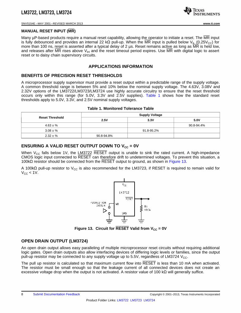
MANUAL RESET INPUT (MR)
Many µP-based products require a manual reset capability, allowing the operator to initiate a reset. The MR inputis fully debounced and provides an internal 22 kΩ pull-up. When the MR input is pulled below VIL (0.25VCC) formore than 100 ns, reset is asserted after a typical delay of 2 µs. Reset remains active as long as MR is held low,and releases after MR rises above VIH and the reset timeout period expires. Use MR with digital logic to assertreset or to daisy chain supervisory circuits.
APPLICATIONS INFORMATION
BENEFITS OF PRECISION RESET THRESHOLDS
A microprocessor supply supervisor must provide a reset output within a predictable range of the supply voltage.A common threshold range is between 5% and 10% below the nominal supply voltage. The 4.63V, 3.08V and2.32V options of the LM3722/LM3723/LM3724 use highly accurate circuitry to ensure that the reset thresholdoccurs only within this range (for 5.0V, 3.3V and 2.5V supplies). Table 1 shows how the standard resetthresholds apply to 5.0V, 3.3V, and 2.5V nominal supply voltages.
Table 1. Monitored Tolerance Table
Supply VoltageReset Threshold
2.5V 3.3V 5.0V
4.63 ± % 90.8-94.4%
3.08 ± % 91.8-95.2%
2.32 ± % 90.8-94.8%
ENSURING A VALID RESET OUTPUT DOWN TO VCC = 0V
When VCC falls below 1V, the LM3722 RESET output is unable to sink the rated current. A high-impedanceCMOS logic input connected to RESET can therefore drift to undetermined voltages. To prevent this situation, a100kΩ resistor should be connected from the RESET output to ground, as shown in Figure 13.
A 100kΩ pull-up resistor to VCC is also recommended for the LM3723, if RESET is required to remain valid forVCC < 1V.
Figure 13. Circuit for RESET Valid from VCC = 0V
OPEN DRAIN OUTPUT (LM3724)
An open drain output allows easy paralleling of multiple microprocessor reset circuits without requiring additionallogic gates. Open drain outputs also allow interfacing devices of differing logic levels or families, since the outputpull-up resistor may be connected to any supply voltage up to 5.5V, regardless of LM3724 VCC.
The pull up resistor is calculated so that maximum current flow into RESET is less than 10 mA when activated.The resistor must be small enough so that the leakage current of all connected devices does not create anexcessive voltage drop when the output is not activated. A resistor value of 100 kΩ will generally suffice.
8 Submit Documentation Feedback Copyright © 2001–2013, Texas Instruments Incorporated
Product Folder Links: LM3722 LM3723 LM3724

0
100
200
300
400
500
600
0 20 40 60 80 100 120 140 160 180 200
Ove
rdriv
e (m
V)
Max Transient Duration (Ps)
LM3722, LM3723, LM3724
www.ti.com SNVS154E –MAY 2001–REVISED MARCH 2013
NEGATIVE-GOING VCC TRANSIENTS
The LM3722/LM3723/LM3724 are relatively immune to short negative-going transients or glitches on VCC.Figure 14 shows the maximum pulse width a negative-going VCC transient can have without causing a resetpulse. In general, as the magnitude of the transient increases, going further below the threshold, the maximumallowable pulse width decreases. Typically, a VCC transient that goes 125 mV below the reset threshold and lasts40 µs or less will not cause a reset pulse. A 0.1 µF bypass capacitor mounted as close as possible to the VCC pinwill provide additional transient rejection.
Figure 14. Maximum Transient Duration without Causing a Reset Pulse vs. Reset Comparator Overdrive
INTERFACING TO µPS WITH BIDIRECTIONAL RESET PINS
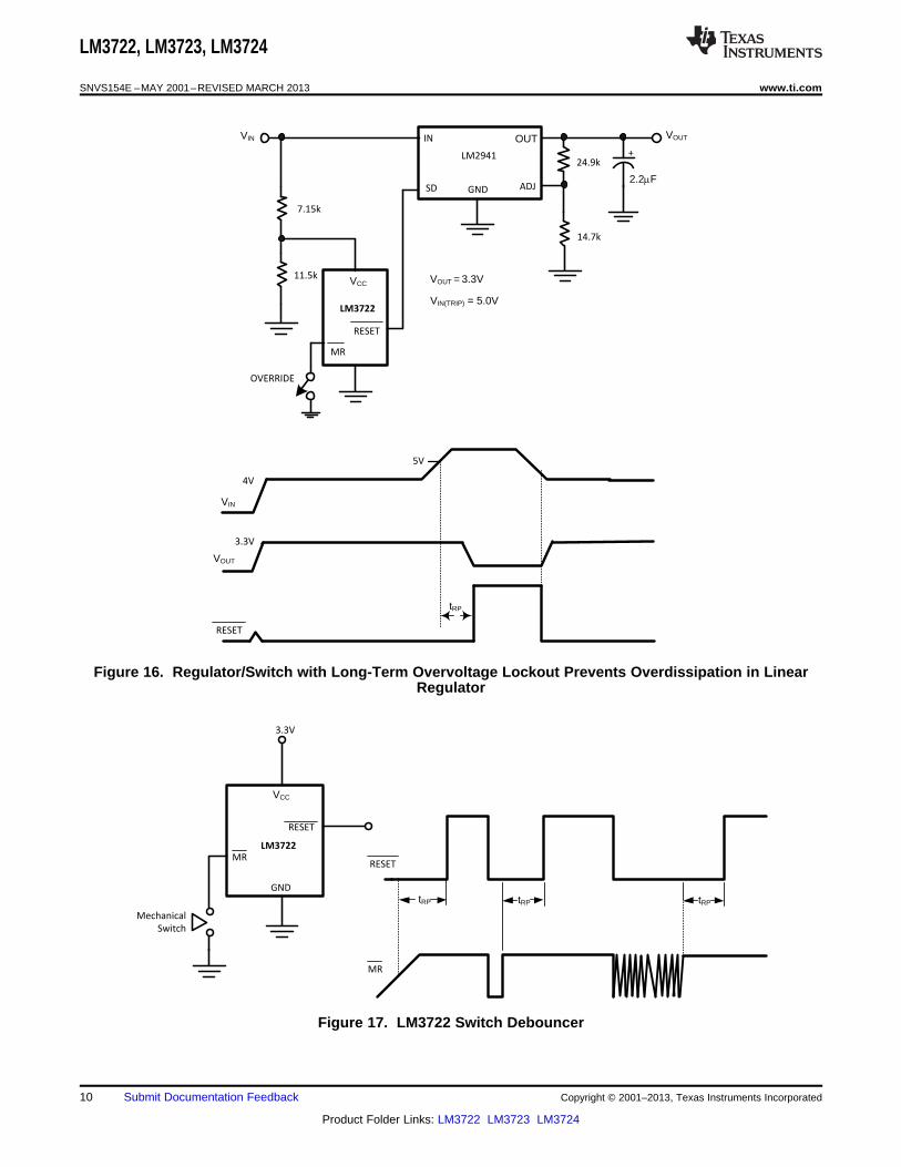
Microprocessors with bidirectional reset pins, such as the Motorola 68HC11 series, can be connected to theLM3722 RESET output. To ensure a correct output on the LM3722 even when the microprocessor reset pin is inthe opposite state, connect a 4.7kΩ resistor between the LM3722 RESET output and the µP reset pin, as shownin Figure 15. Buffer the LM3722 RESET output to other system components.
Typical Application Circuits
Figure 15. Interfacing to Microprocessors with Bidirectional Reset I/O
Copyright © 2001–2013, Texas Instruments Incorporated Submit Documentation Feedback 9
Product Folder Links: LM3722 LM3723 LM3724
GND
3.3V
Mechanical
Switch
VCC
LM3722
RESET
MRRESET
MR
tRP tRP tRP
VCC
MR
LM2941
IN
SD
VIN OUT
OVERRIDE
5V
3.3V
VIN
VOUT
tRP
GND ADJ
VOUT
11.5k
7.15k
24.9k
14.7k
RESET
RESET
VOUT = 3.3V
VIN(TRIP) = 5.0V
2.2PF
+
4V
LM3722
LM3722, LM3723, LM3724
SNVS154E –MAY 2001–REVISED MARCH 2013 www.ti.com
Figure 16. Regulator/Switch with Long-Term Overvoltage Lockout Prevents Overdissipation in LinearRegulator
Figure 17. LM3722 Switch Debouncer
10 Submit Documentation Feedback Copyright © 2001–2013, Texas Instruments Incorporated
Product Folder Links: LM3722 LM3723 LM3724
RESET
VIN
R
C
VOUT
LOAD
MTP50P03HDL
VCC
GND
VIN
VOUT
RESET
tRP
LM3723
LM3722, LM3723, LM3724
www.ti.com SNVS154E –MAY 2001–REVISED MARCH 2013
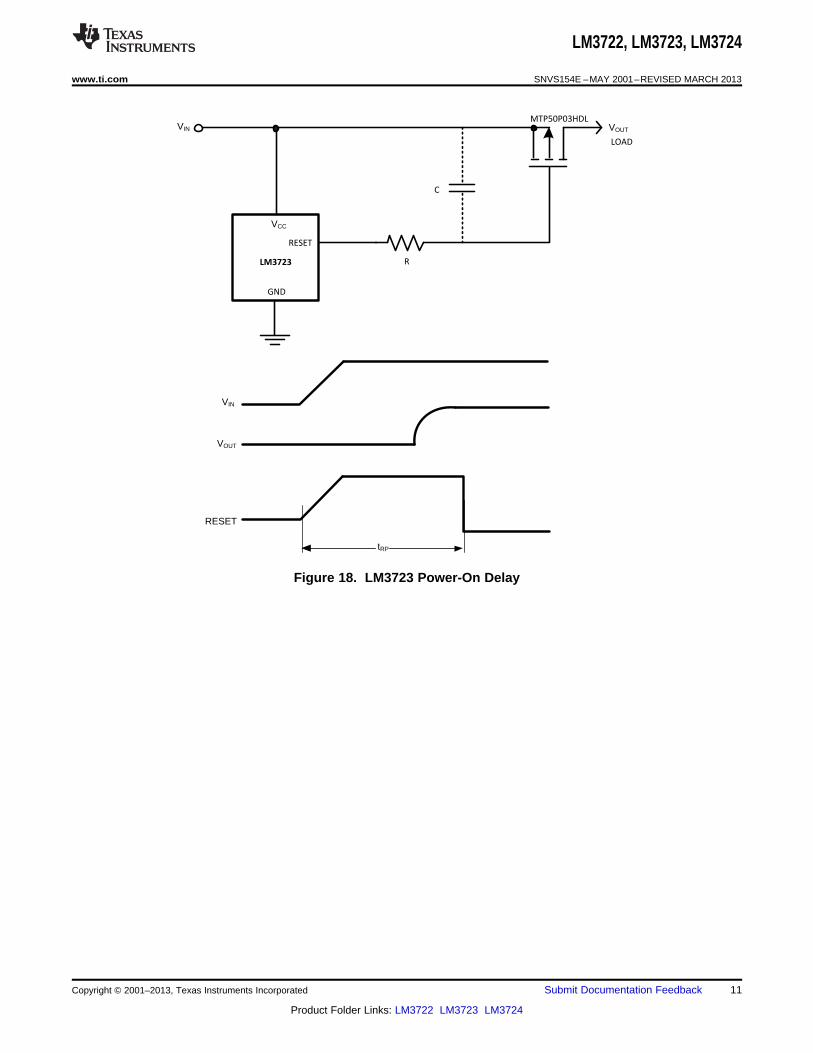
Figure 18. LM3723 Power-On Delay
Copyright © 2001–2013, Texas Instruments Incorporated Submit Documentation Feedback 11
Product Folder Links: LM3722 LM3723 LM3724
LM3722, LM3723, LM3724
SNVS154E –MAY 2001–REVISED MARCH 2013 www.ti.com
REVISION HISTORY
Changes from Revision D (March 2013) to Revision E Page
• Changed layout of National Data Sheet to TI format .......................................................................................................... 11
12 Submit Documentation Feedback Copyright © 2001–2013, Texas Instruments Incorporated
Product Folder Links: LM3722 LM3723 LM3724

PACKAGE OPTION ADDENDUM
www.ti.com 8-Oct-2015
Addendum-Page 1
PACKAGING INFORMATION
Orderable Device Status(1)
Package Type PackageDrawing
Pins PackageQty
Eco Plan(2)
Lead/Ball Finish(6)
MSL Peak Temp(3)
Op Temp (°C) Device Marking(4/5)
Samples
LM3724EM5-3.08/NOPB ACTIVE SOT-23 DBV 5 1000 Green (RoHS& no Sb/Br)
CU SN Level-1-260C-UNLIM -40 to 125 R63B
LM3724EM5-4.63/NOPB ACTIVE SOT-23 DBV 5 1000 Green (RoHS& no Sb/Br)
CU SN Level-1-260C-UNLIM -40 to 125 R62B
LM3724IM5-2.32/NOPB ACTIVE SOT-23 DBV 5 1000 Green (RoHS& no Sb/Br)
CU SN Level-1-260C-UNLIM -40 to 85 R50B
LM3724IM5-3.08/NOPB ACTIVE SOT-23 DBV 5 1000 Green (RoHS& no Sb/Br)
CU SN Level-1-260C-UNLIM -40 to 85 R53B
LM3724IM5-4.63/NOPB ACTIVE SOT-23 DBV 5 1000 Green (RoHS& no Sb/Br)
CU SN Level-1-260C-UNLIM -40 to 85 R55B
LM3724IM5X-3.08/NOPB ACTIVE SOT-23 DBV 5 3000 Green (RoHS& no Sb/Br)
CU SN Level-1-260C-UNLIM -40 to 85 R53B
(1) The marketing status values are defined as follows:ACTIVE: Product device recommended for new designs.LIFEBUY: TI has announced that the device will be discontinued, and a lifetime-buy period is in effect.NRND: Not recommended for new designs. Device is in production to support existing customers, but TI does not recommend using this part in a new design.PREVIEW: Device has been announced but is not in production. Samples may or may not be available.OBSOLETE: TI has discontinued the production of the device.
(2) Eco Plan - The planned eco-friendly classification: Pb-Free (RoHS), Pb-Free (RoHS Exempt), or Green (RoHS & no Sb/Br) - please check http://www.ti.com/productcontent for the latest availabilityinformation and additional product content details.TBD: The Pb-Free/Green conversion plan has not been defined.Pb-Free (RoHS): TI's terms "Lead-Free" or "Pb-Free" mean semiconductor products that are compatible with the current RoHS requirements for all 6 substances, including the requirement thatlead not exceed 0.1% by weight in homogeneous materials. Where designed to be soldered at high temperatures, TI Pb-Free products are suitable for use in specified lead-free processes.Pb-Free (RoHS Exempt): This component has a RoHS exemption for either 1) lead-based flip-chip solder bumps used between the die and package, or 2) lead-based die adhesive used betweenthe die and leadframe. The component is otherwise considered Pb-Free (RoHS compatible) as defined above.Green (RoHS & no Sb/Br): TI defines "Green" to mean Pb-Free (RoHS compatible), and free of Bromine (Br) and Antimony (Sb) based flame retardants (Br or Sb do not exceed 0.1% by weightin homogeneous material)
(3) MSL, Peak Temp. - The Moisture Sensitivity Level rating according to the JEDEC industry standard classifications, and peak solder temperature.
(4) There may be additional marking, which relates to the logo, the lot trace code information, or the environmental category on the device.
(5) Multiple Device Markings will be inside parentheses. Only one Device Marking contained in parentheses and separated by a "~" will appear on a device. If a line is indented then it is a continuationof the previous line and the two combined represent the entire Device Marking for that device.
PACKAGE OPTION ADDENDUM
www.ti.com 8-Oct-2015
Addendum-Page 2
(6) Lead/Ball Finish - Orderable Devices may have multiple material finish options. Finish options are separated by a vertical ruled line. Lead/Ball Finish values may wrap to two lines if the finishvalue exceeds the maximum column width.
Important Information and Disclaimer:The information provided on this page represents TI's knowledge and belief as of the date that it is provided. TI bases its knowledge and belief on informationprovided by third parties, and makes no representation or warranty as to the accuracy of such information. Efforts are underway to better integrate information from third parties. TI has taken andcontinues to take reasonable steps to provide representative and accurate information but may not have conducted destructive testing or chemical analysis on incoming materials and chemicals.TI and TI suppliers consider certain information to be proprietary, and thus CAS numbers and other limited information may not be available for release.
In no event shall TI's liability arising out of such information exceed the total purchase price of the TI part(s) at issue in this document sold by TI to Customer on an annual basis.
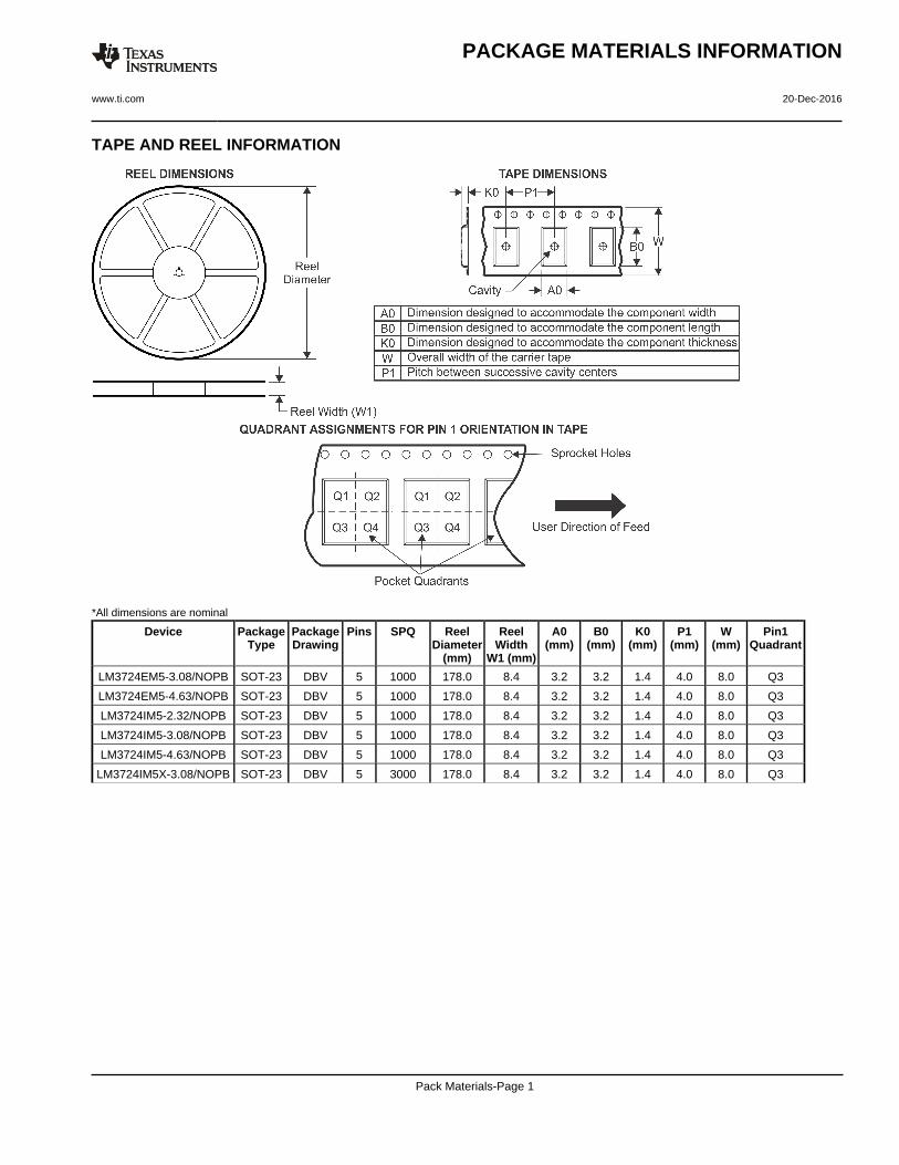
TAPE AND REEL INFORMATION
*All dimensions are nominal
Device PackageType
PackageDrawing
Pins SPQ ReelDiameter
(mm)
ReelWidth
W1 (mm)
A0(mm)
B0(mm)
K0(mm)
P1(mm)
W(mm)
Pin1Quadrant
LM3724EM5-3.08/NOPB SOT-23 DBV 5 1000 178.0 8.4 3.2 3.2 1.4 4.0 8.0 Q3
LM3724EM5-4.63/NOPB SOT-23 DBV 5 1000 178.0 8.4 3.2 3.2 1.4 4.0 8.0 Q3
LM3724IM5-2.32/NOPB SOT-23 DBV 5 1000 178.0 8.4 3.2 3.2 1.4 4.0 8.0 Q3
LM3724IM5-3.08/NOPB SOT-23 DBV 5 1000 178.0 8.4 3.2 3.2 1.4 4.0 8.0 Q3
LM3724IM5-4.63/NOPB SOT-23 DBV 5 1000 178.0 8.4 3.2 3.2 1.4 4.0 8.0 Q3
LM3724IM5X-3.08/NOPB SOT-23 DBV 5 3000 178.0 8.4 3.2 3.2 1.4 4.0 8.0 Q3
PACKAGE MATERIALS INFORMATION
www.ti.com 20-Dec-2016
Pack Materials-Page 1

*All dimensions are nominal
Device Package Type Package Drawing Pins SPQ Length (mm) Width (mm) Height (mm)
LM3724EM5-3.08/NOPB SOT-23 DBV 5 1000 210.0 185.0 35.0
LM3724EM5-4.63/NOPB SOT-23 DBV 5 1000 210.0 185.0 35.0
LM3724IM5-2.32/NOPB SOT-23 DBV 5 1000 210.0 185.0 35.0
LM3724IM5-3.08/NOPB SOT-23 DBV 5 1000 210.0 185.0 35.0
LM3724IM5-4.63/NOPB SOT-23 DBV 5 1000 210.0 185.0 35.0
LM3724IM5X-3.08/NOPB SOT-23 DBV 5 3000 210.0 185.0 35.0
PACKAGE MATERIALS INFORMATION
www.ti.com 20-Dec-2016
Pack Materials-Page 2

www.ti.com
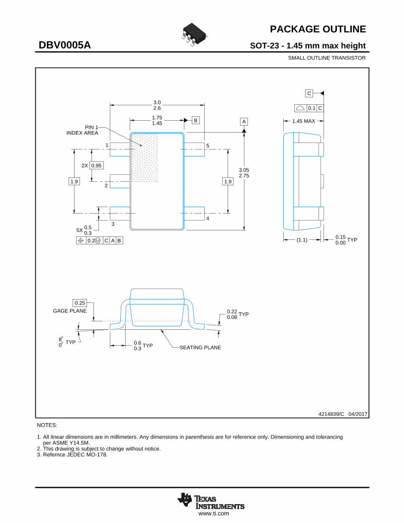
PACKAGE OUTLINE
C
TYP0.220.08
0.25
3.02.6
2X 0.95
1.9
1.45 MAX
TYP0.150.00
5X 0.50.3
TYP0.60.3
TYP80
1.9
A
3.052.75
B1.751.45
(1.1)
SOT-23 - 1.45 mm max heightDBV0005ASMALL OUTLINE TRANSISTOR
4214839/C 04/2017
NOTES: 1. All linear dimensions are in millimeters. Any dimensions in parenthesis are for reference only. Dimensioning and tolerancing per ASME Y14.5M.2. This drawing is subject to change without notice.3. Refernce JEDEC MO-178.
0.2 C A B
1
34
5
2
INDEX AREAPIN 1
GAGE PLANE
SEATING PLANE
0.1 C
SCALE 4.000
www.ti.com
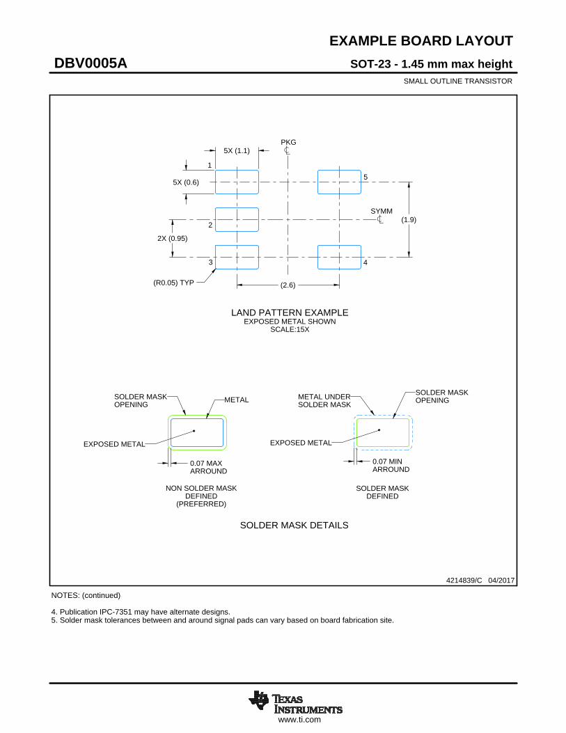
EXAMPLE BOARD LAYOUT
0.07 MAXARROUND
0.07 MINARROUND
5X (1.1)
5X (0.6)
(2.6)
(1.9)
2X (0.95)
(R0.05) TYP
4214839/C 04/2017
SOT-23 - 1.45 mm max heightDBV0005ASMALL OUTLINE TRANSISTOR
NOTES: (continued) 4. Publication IPC-7351 may have alternate designs. 5. Solder mask tolerances between and around signal pads can vary based on board fabrication site.
SYMM
LAND PATTERN EXAMPLEEXPOSED METAL SHOWN
SCALE:15X
PKG
1
3 4
5
2
SOLDER MASKOPENINGMETAL UNDER
SOLDER MASK
SOLDER MASKDEFINED
EXPOSED METAL
METALSOLDER MASKOPENING
NON SOLDER MASKDEFINED
(PREFERRED)
SOLDER MASK DETAILS
EXPOSED METAL

www.ti.com
EXAMPLE STENCIL DESIGN
(2.6)
(1.9)
2X(0.95)
5X (1.1)
5X (0.6)
(R0.05) TYP
SOT-23 - 1.45 mm max heightDBV0005ASMALL OUTLINE TRANSISTOR
4214839/C 04/2017
NOTES: (continued) 6. Laser cutting apertures with trapezoidal walls and rounded corners may offer better paste release. IPC-7525 may have alternate design recommendations. 7. Board assembly site may have different recommendations for stencil design.
SOLDER PASTE EXAMPLEBASED ON 0.125 mm THICK STENCIL
SCALE:15X
SYMM
PKG
1
3 4
5
2

www.ti.com
PACKAGE OUTLINE
C
TYP0.220.08
0.25
3.02.6
2X 0.95
1.9
1.45 MAX
TYP0.150.00
5X 0.50.3
TYP0.60.3
TYP80
1.9
A
3.052.75
B1.751.45
(1.1)
SOT-23 - 1.45 mm max heightDBV0005ASMALL OUTLINE TRANSISTOR
4214839/C 04/2017
NOTES: 1. All linear dimensions are in millimeters. Any dimensions in parenthesis are for reference only. Dimensioning and tolerancing per ASME Y14.5M.2. This drawing is subject to change without notice.3. Refernce JEDEC MO-178.
0.2 C A B
1
34
5
2
INDEX AREAPIN 1
GAGE PLANE
SEATING PLANE
0.1 C
SCALE 4.000

www.ti.com
EXAMPLE BOARD LAYOUT
0.07 MAXARROUND
0.07 MINARROUND
5X (1.1)
5X (0.6)
(2.6)
(1.9)
2X (0.95)
(R0.05) TYP
4214839/C 04/2017
SOT-23 - 1.45 mm max heightDBV0005ASMALL OUTLINE TRANSISTOR
NOTES: (continued) 4. Publication IPC-7351 may have alternate designs. 5. Solder mask tolerances between and around signal pads can vary based on board fabrication site.
SYMM
LAND PATTERN EXAMPLEEXPOSED METAL SHOWN
SCALE:15X
PKG
1
3 4
5
2
SOLDER MASKOPENINGMETAL UNDER
SOLDER MASK
SOLDER MASKDEFINED
EXPOSED METAL
METALSOLDER MASKOPENING
NON SOLDER MASKDEFINED
(PREFERRED)
SOLDER MASK DETAILS
EXPOSED METAL

www.ti.com
EXAMPLE STENCIL DESIGN
(2.6)
(1.9)
2X(0.95)
5X (1.1)
5X (0.6)
(R0.05) TYP
SOT-23 - 1.45 mm max heightDBV0005ASMALL OUTLINE TRANSISTOR
4214839/C 04/2017
NOTES: (continued) 6. Laser cutting apertures with trapezoidal walls and rounded corners may offer better paste release. IPC-7525 may have alternate design recommendations. 7. Board assembly site may have different recommendations for stencil design.
SOLDER PASTE EXAMPLEBASED ON 0.125 mm THICK STENCIL
SCALE:15X
SYMM
PKG
1
3 4
5
2

IMPORTANT NOTICE
Texas Instruments Incorporated (TI) reserves the right to make corrections, enhancements, improvements and other changes to itssemiconductor products and services per JESD46, latest issue, and to discontinue any product or service per JESD48, latest issue. Buyersshould obtain the latest relevant information before placing orders and should verify that such information is current and complete.TI’s published terms of sale for semiconductor products (http://www.ti.com/sc/docs/stdterms.htm) apply to the sale of packaged integratedcircuit products that TI has qualified and released to market. Additional terms may apply to the use or sale of other types of TI products andservices.Reproduction of significant portions of TI information in TI data sheets is permissible only if reproduction is without alteration and isaccompanied by all associated warranties, conditions, limitations, and notices. TI is not responsible or liable for such reproduceddocumentation. Information of third parties may be subject to additional restrictions. Resale of TI products or services with statementsdifferent from or beyond the parameters stated by TI for that product or service voids all express and any implied warranties for theassociated TI product or service and is an unfair and deceptive business practice. TI is not responsible or liable for any such statements.Buyers and others who are developing systems that incorporate TI products (collectively, “Designers”) understand and agree that Designersremain responsible for using their independent analysis, evaluation and judgment in designing their applications and that Designers havefull and exclusive responsibility to assure the safety of Designers' applications and compliance of their applications (and of all TI productsused in or for Designers’ applications) with all applicable regulations, laws and other applicable requirements. Designer represents that, withrespect to their applications, Designer has all the necessary expertise to create and implement safeguards that (1) anticipate dangerousconsequences of failures, (2) monitor failures and their consequences, and (3) lessen the likelihood of failures that might cause harm andtake appropriate actions. Designer agrees that prior to using or distributing any applications that include TI products, Designer willthoroughly test such applications and the functionality of such TI products as used in such applications.TI’s provision of technical, application or other design advice, quality characterization, reliability data or other services or information,including, but not limited to, reference designs and materials relating to evaluation modules, (collectively, “TI Resources”) are intended toassist designers who are developing applications that incorporate TI products; by downloading, accessing or using TI Resources in anyway, Designer (individually or, if Designer is acting on behalf of a company, Designer’s company) agrees to use any particular TI Resourcesolely for this purpose and subject to the terms of this Notice.TI’s provision of TI Resources does not expand or otherwise alter TI’s applicable published warranties or warranty disclaimers for TIproducts, and no additional obligations or liabilities arise from TI providing such TI Resources. TI reserves the right to make corrections,enhancements, improvements and other changes to its TI Resources. TI has not conducted any testing other than that specificallydescribed in the published documentation for a particular TI Resource.Designer is authorized to use, copy and modify any individual TI Resource only in connection with the development of applications thatinclude the TI product(s) identified in such TI Resource. NO OTHER LICENSE, EXPRESS OR IMPLIED, BY ESTOPPEL OR OTHERWISETO ANY OTHER TI INTELLECTUAL PROPERTY RIGHT, AND NO LICENSE TO ANY TECHNOLOGY OR INTELLECTUAL PROPERTYRIGHT OF TI OR ANY THIRD PARTY IS GRANTED HEREIN, including but not limited to any patent right, copyright, mask work right, orother intellectual property right relating to any combination, machine, or process in which TI products or services are used. Informationregarding or referencing third-party products or services does not constitute a license to use such products or services, or a warranty orendorsement thereof. Use of TI Resources may require a license from a third party under the patents or other intellectual property of thethird party, or a license from TI under the patents or other intellectual property of TI.TI RESOURCES ARE PROVIDED “AS IS” AND WITH ALL FAULTS. TI DISCLAIMS ALL OTHER WARRANTIES ORREPRESENTATIONS, EXPRESS OR IMPLIED, REGARDING RESOURCES OR USE THEREOF, INCLUDING BUT NOT LIMITED TOACCURACY OR COMPLETENESS, TITLE, ANY EPIDEMIC FAILURE WARRANTY AND ANY IMPLIED WARRANTIES OFMERCHANTABILITY, FITNESS FOR A PARTICULAR PURPOSE, AND NON-INFRINGEMENT OF ANY THIRD PARTY INTELLECTUALPROPERTY RIGHTS. TI SHALL NOT BE LIABLE FOR AND SHALL NOT DEFEND OR INDEMNIFY DESIGNER AGAINST ANY CLAIM,INCLUDING BUT NOT LIMITED TO ANY INFRINGEMENT CLAIM THAT RELATES TO OR IS BASED ON ANY COMBINATION OFPRODUCTS EVEN IF DESCRIBED IN TI RESOURCES OR OTHERWISE. IN NO EVENT SHALL TI BE LIABLE FOR ANY ACTUAL,DIRECT, SPECIAL, COLLATERAL, INDIRECT, PUNITIVE, INCIDENTAL, CONSEQUENTIAL OR EXEMPLARY DAMAGES INCONNECTION WITH OR ARISING OUT OF TI RESOURCES OR USE THEREOF, AND REGARDLESS OF WHETHER TI HAS BEENADVISED OF THE POSSIBILITY OF SUCH DAMAGES.Unless TI has explicitly designated an individual product as meeting the requirements of a particular industry standard (e.g., ISO/TS 16949and ISO 26262), TI is not responsible for any failure to meet such industry standard requirements.Where TI specifically promotes products as facilitating functional safety or as compliant with industry functional safety standards, suchproducts are intended to help enable customers to design and create their own applications that meet applicable functional safety standardsand requirements. Using products in an application does not by itself establish any safety features in the application. Designers mustensure compliance with safety-related requirements and standards applicable to their applications. Designer may not use any TI products inlife-critical medical equipment unless authorized officers of the parties have executed a special contract specifically governing such use.Life-critical medical equipment is medical equipment where failure of such equipment would cause serious bodily injury or death (e.g., lifesupport, pacemakers, defibrillators, heart pumps, neurostimulators, and implantables). Such equipment includes, without limitation, allmedical devices identified by the U.S. Food and Drug Administration as Class III devices and equivalent classifications outside the U.S.TI may expressly designate certain products as completing a particular qualification (e.g., Q100, Military Grade, or Enhanced Product).Designers agree that it has the necessary expertise to select the product with the appropriate qualification designation for their applicationsand that proper product selection is at Designers’ own risk. Designers are solely responsible for compliance with all legal and regulatoryrequirements in connection with such selection.Designer will fully indemnify TI and its representatives against any damages, costs, losses, and/or liabilities arising out of Designer’s non-compliance with the terms and provisions of this Notice.
Mailing Address: Texas Instruments, Post Office Box 655303, Dallas, Texas 75265Copyright © 2018, Texas Instruments Incorporated