Timing Diagram of 8085
13
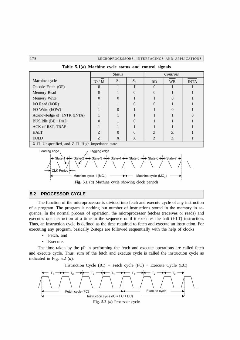
5.1 INTRODUCTION Timing diagram is the display of initiation of read/write and transfer of data operations under the control of 3-status signals IO / M , S 1 , and S 0 . As the heartbeat is required for the survival of the human being, the CLK is required for the proper operation of different sections of the microprocessors. All actions in the microprocessor is controlled by either leading or trailing edge of the clock. If I ask a man to bring 6-bags of wheat, each weighing 100 kg, he may take 6-times to perform this task in going and bringing it. A stronger man might perform the same task in 3- times only. Thus, it depends on the strength of the man to finish the job quickly or slowly. Here, we can assume both weaker and strong men as machine. The weaker man has taken 6-machine cycle (6-times going and coming with one bag each time) to execute the job where as the stronger man has taken only 3-machine cycle for the same job. Similarly, a machine may execute one instruction in as many as 3-machine cycles while the other machine can take only one machine cycle to execute the same instruction. Thus, the machine that has taken only one machine cycle is efficient than the one taking 3-machine cycle. Each machine cycle is composed of many clock cycle. Since, the data and instructions, both are stored in the memory, the μP performs fetch operation to read the instruction or data and then execute the instruction. The μP in doing so may take several cycles to perform fetch and execute operation. The 3-status signals : IO / M , S 1 , and S 0 are generated at the beginning of each machine cycle. The unique combination of these 3-status signals identify read or write operation and remain valid for the duration of the cycle. Table-5.1(a) shows details of the unique combination of these status signals to identify different machine cycles. Thus, time taken by any μP to execute one instruction is calculated in terms of the clock period. The execution of instruction always requires read and writes operations to transfer data to or from the μP and memory or I/O devices. Each read/ write operation constitutes one machine cycle (MC 1 ) as indicated in Fig. 5.1 (a). Each machine cycle consists of many clock periods/ cycles, called T-states. The heartbeat of the microprocessor is the clock period. Each and every operation inside the microprocessor is under the control of the clock cycle. The clock signal determines the time taken by the microprocessor to execute any instruction. The clock cycle shown in Fig. 5.1 (a) has two edges (leading and trailing or lagging). State is defined as the time interval between 2-trailing or leading edges of the clock. Machine cycle is the time required to transfer data to or from memory or I/O devices. 177 TIMING DIAGRAM O 8085 5
Transcript of Timing Diagram of 8085

5.1 INTRODUCTION
Timing diagram is the display of initiation of read/write and transfer of data operations underthe control of 3-status signals IO / M , S1, and S0. As the heartbeat is required for the survivalof the human being, the CLK is required for the proper operation of different sections of themicroprocessors. All actions in the microprocessor is controlled by either leading or trailing edgeof the clock. If I ask a man to bring 6-bags of wheat, each weighing 100 kg, he may take 6-timesto perform this task in going and bringing it. A stronger man might perform the same task in 3-times only. Thus, it depends on the strength of the man to finish the job quickly or slowly. Here,we can assume both weaker and strong men as machine. The weaker man has taken 6-machinecycle (6-times going and coming with one bag each time) to execute the job where as the strongerman has taken only 3-machine cycle for the same job. Similarly, a machine may execute oneinstruction in as many as 3-machine cycles while the other machine can take only one machinecycle to execute the same instruction. Thus, the machine that has taken only one machine cycleis efficient than the one taking 3-machine cycle. Each machine cycle is composed of many clockcycle. Since, the data and instructions, both are stored in the memory, the µP performs fetchoperation to read the instruction or data and then execute the instruction. The µP in doing so maytake several cycles to perform fetch and execute operation. The 3-status signals : IO / M , S1, andS0 are generated at the beginning of each machine cycle. The unique combination of these 3-statussignals identify read or write operation and remain valid for the duration of the cycle. Table-5.1(a)shows details of the unique combination of these status signals to identify different machine cycles.Thus, time taken by any µP to execute one instruction is calculated in terms of the clock period.
The execution of instruction always requires read and writes operations to transfer data toor from the µP and memory or I/O devices. Each read/ write operation constitutes one machinecycle (MC1) as indicated in Fig. 5.1 (a). Each machine cycle consists of many clock periods/cycles, called T-states. The heartbeat of the microprocessor is the clock period. Each and everyoperation inside the microprocessor is under the control of the clock cycle. The clock signaldetermines the time taken by the microprocessor to execute any instruction. The clock cycleshown in Fig. 5.1 (a) has two edges (leading and trailing or lagging). State is defined as the timeinterval between 2-trailing or leading edges of the clock. Machine cycle is the time required totransfer data to or from memory or I/O devices.
177
������� ������� �� � ��
5
178 MICROPROCESSORS, INTERFACINGS AND APPLICATIONS
Table 5.1(a) Machine cycle status and control signals
Status Controls
Machine cycle IO / M S1 S0 RD WR INTAOpcode Fetch (OF) 0 1 1 0 1 1
Memory Read 0 1 0 0 1 1
Memory Write 0 0 1 1 0 1
I/O Read (I/OR) 1 1 0 0 1 1I/O Write (I/OW) 1 0 1 1 0 1
Acknowledge of INTR (INTA) 1 1 1 1 1 0
BUS Idle (BI) : DAD 0 1 0 1 1 1
ACK of RST, TRAP 1 1 1 1 1 1
HALT Z 0 0 Z Z 1
HOLD Z X X Z Z 1
X ⇒ Unspecified, and Z ⇒ High impedance state
Fig. 5.1 (a) Machine cycle showing clock periods
5.2 PROCESSOR CYCLE
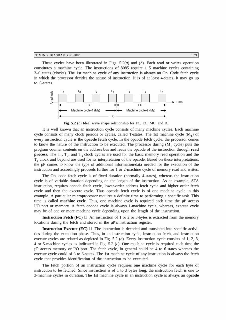
The function of the microprocessor is divided into fetch and execute cycle of any instructionof a program. The program is nothing but number of instructions stored in the memory in se-quence. In the normal process of operation, the microprocessor fetches (receives or reads) andexecutes one instruction at a time in the sequence until it executes the halt (HLT) instruction.Thus, an instruction cycle is defined as the time required to fetch and execute an instruction. Forexecuting any program, basically 2-steps are followed sequentially with the help of clocks
• Fetch, and
• Execute.
The time taken by the µP in performing the fetch and execute operations are called fetchand execute cycle. Thus, sum of the fetch and execute cycle is called the instruction cycle asindicated in Fig. 5.2 (a).
Instruction Cycle (IC) = Fetch cycle (FC) + Execute Cycle (EC)
Fig. 5.2 (a) Processor cycle
TIMING DIAGRAM OF 8085 179
These cycles have been illustrated in Figs. 5.2(a) and (b). Each read or writes operationconstitutes a machine cycle. The instructions of 8085 require 1–5 machine cycles containing3–6 states (clocks). The 1st machine cycle of any instruction is always an Op. Code fetch cyclein which the processor decides the nature of instruction. It is of at least 4-states. It may go upto 6-states.
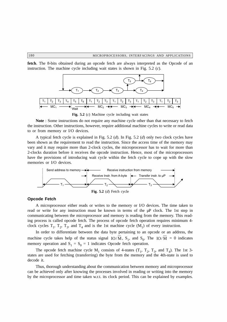
Fig. 5.2 (b) Ideal wave shape relationship for FC, EC, MC, and IC.
It is well known that an instruction cycle consists of many machine cycles. Each machinecycle consists of many clock periods or cycles, called T-states. The 1st machine cycle (M1) ofevery instruction cycle is the opcode fetch cycle. In the opcode fetch cycle, the processor comesto know the nature of the instruction to be executed. The processor during (M1 cycle) puts theprogram counter contents on the address bus and reads the opcode of the instruction through readprocess. The T1, T2, and T3 clock cycles are used for the basic memory read operation and theT4 clock and beyond are used for its interpretation of the opcode. Based on these interpretations,the µP comes to know the type of additional information/data needed for the execution of theinstruction and accordingly proceeds further for 1 or 2-machine cycle of memory read and writes.
The Op. code fetch cycle is of fixed duration (normally 4-states), whereas the instructioncycle is of variable duration depending on the length of the instruction. As an example, STAinstruction, requires opcode fetch cycle, lower-order address fetch cycle and higher order fetchcycle and then the execute cycle. Thus opcode fetch cycle is of one machine cycle in thisexample. A particular microprocessor requires a definite time to performing a specific task. Thistime is called machine cycle. Thus, one machine cycle is required each time the µP accessI/O port or memory. A fetch opcode cycle is always 1-machine cycle, whereas, execute cyclemay be of one or more machine cycle depending upon the length of the instruction.
Instruction Fetch (FC) ⇒ An instruction of 1 or 2 or 3-bytes is extracted from the memorylocations during the fetch and stored in the µP’s instruction register.
Instruction Execute (EC) ⇒ The instruction is decoded and translated into specific activi-ties during the execution phase. Thus, in an instruction cycle, instruction fetch, and instructionexecute cycles are related as depicted in Fig. 5.2 (a). Every instruction cycle consists of 1, 2, 3,4 or 5-machine cycles as indicated in Fig. 5.2 (c). One machine cycle is required each time theµP access memory or I/O port. The fetch cycle, in general could be 4 to 6-states whereas theexecute cycle could of 3 to 6-states. The 1st machine cycle of any instruction is always the fetchcycle that provides identification of the instruction to be executed.
The fetch portion of an instruction cycle requires one machine cycle for each byte ofinstruction to be fetched. Since instruction is of 1 to 3 bytes long, the instruction fetch is one to3-machine cycles in duration. The 1st machine cycle in an instruction cycle is always an opcode
180 MICROPROCESSORS, INTERFACINGS AND APPLICATIONS
fetch. The 8-bits obtained during an opcode fetch are always interpreted as the Opcode of aninstruction. The machine cycle including wait states is shown in Fig. 5.2 (c).
Fig. 5.2 (c) Machine cycle including wait states
Note : Some instructions do not require any machine cycle other than that necessary to fetchthe instruction. Other instructions, however, require additional machine cycles to write or read datato or from memory or I/O devices.
A typical fetch cycle is explained in Fig. 5.2 (d). In Fig. 5.2 (d) only two clock cycles havebeen shown as the requirement to read the instruction. Since the access time of the memory mayvary and it may require more than 2-clock cycles, the microprocessor has to wait for more than2-clocks duration before it receives the opcode instruction. Hence, most of the microprocessorshave the provisions of introducing wait cycle within the fetch cycle to cope up with the slowmemories or I/O devices.
Fig. 5.2 (d) Fetch cycle
Opcode Fetch
A microprocessor either reads or writes to the memory or I/O devices. The time taken toread or write for any instruction must be known in terms of the µP clock. The 1st step incommunicating between the microprocessor and memory is reading from the memory. This read-ing process is called opcode fetch. The process of opcode fetch operation requires minimum 4-clock cycles T1, T2, T3, and T4 and is the 1st machine cycle (M1) of every instruction.
In order to differentiate between the data byte pertaining to an opcode or an address, the
machine cycle takes help of the status signal IO/ M , S1, and S0. The IO/ M = 0 indicatesmemory operation and S1 = S0 = 1 indicates Opcode fetch operation.
The opcode fetch machine cycle M1 consists of 4-states (T1, T2, T3, and T4). The 1st 3-states are used for fetching (transferring) the byte from the memory and the 4th-state is used todecode it.
Thus, thorough understanding about the communication between memory and microprocessorcan be achieved only after knowing the processes involved in reading or writing into the memoryby the microprocessor and time taken w.r.t. its clock period. This can be explained by examples.
TIMING DIAGRAM OF 8085 181
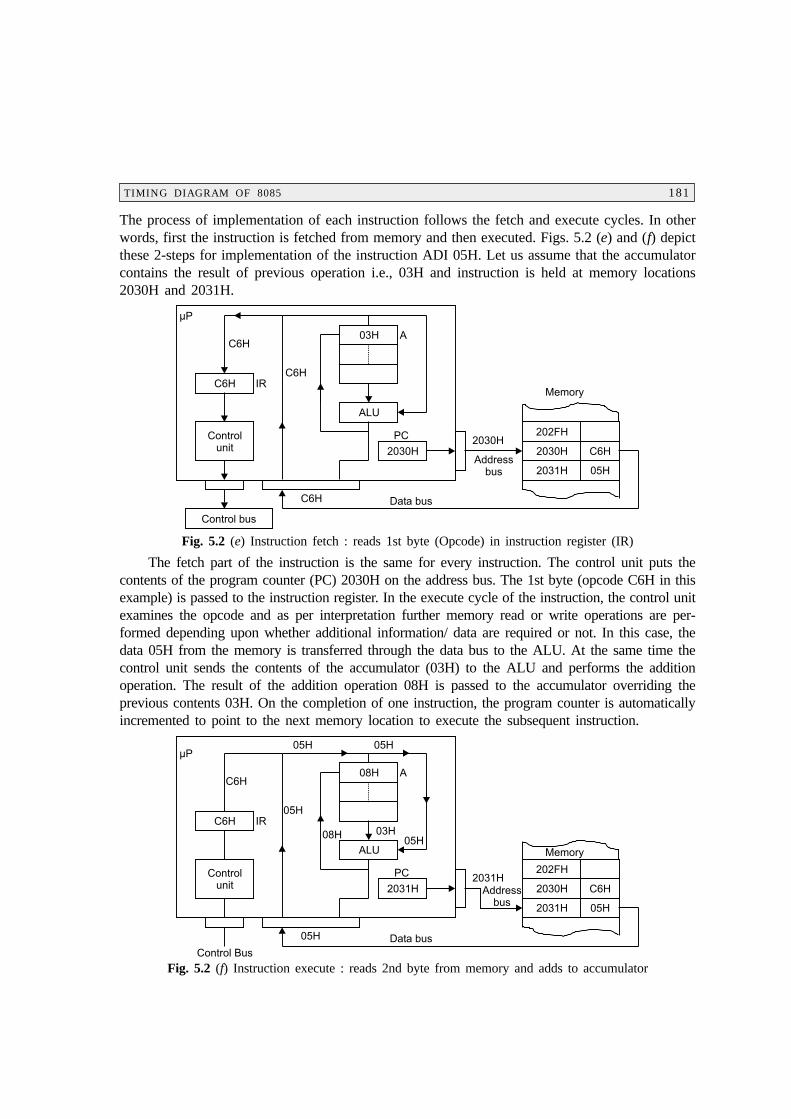
The process of implementation of each instruction follows the fetch and execute cycles. In otherwords, first the instruction is fetched from memory and then executed. Figs. 5.2 (e) and (f) depictthese 2-steps for implementation of the instruction ADI 05H. Let us assume that the accumulatorcontains the result of previous operation i.e., 03H and instruction is held at memory locations2030H and 2031H.
Fig. 5.2 (e) Instruction fetch : reads 1st byte (Opcode) in instruction register (IR)
The fetch part of the instruction is the same for every instruction. The control unit puts thecontents of the program counter (PC) 2030H on the address bus. The 1st byte (opcode C6H in thisexample) is passed to the instruction register. In the execute cycle of the instruction, the control unitexamines the opcode and as per interpretation further memory read or write operations are per-formed depending upon whether additional information/ data are required or not. In this case, thedata 05H from the memory is transferred through the data bus to the ALU. At the same time thecontrol unit sends the contents of the accumulator (03H) to the ALU and performs the additionoperation. The result of the addition operation 08H is passed to the accumulator overriding theprevious contents 03H. On the completion of one instruction, the program counter is automaticallyincremented to point to the next memory location to execute the subsequent instruction.
Fig. 5.2 (f) Instruction execute : reads 2nd byte from memory and adds to accumulator
182 MICROPROCESSORS, INTERFACINGS AND APPLICATIONS
Note : The slope of the edges of the clock pulses has been shown to be much exaggeratedto indicate the existence of rise and fall time.
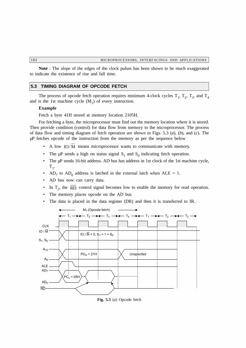
5.3 TIMING DIAGRAM OF OPCODE FETCH
The process of opcode fetch operation requires minimum 4-clock cycles T1, T2, T3, and T4and is the 1st machine cycle (M1) of every instruction.
Example
Fetch a byte 41H stored at memory location 2105H.
For fetching a byte, the microprocessor must find out the memory location where it is stored.Then provide condition (control) for data flow from memory to the microprocessor. The processof data flow and timing diagram of fetch operation are shown in Figs. 5.3 (a), (b), and (c). TheµP fetches opcode of the instruction from the memory as per the sequence below
• A low IO/ M means microprocessor wants to communicate with memory.
• The µP sends a high on status signal S1 and S0 indicating fetch operation.
• The µP sends 16-bit address. AD bus has address in 1st clock of the 1st machine cycle,T1.
• AD7 to AD0 address is latched in the external latch when ALE = 1.
• AD bus now can carry data.
• In T2, the RD control signal becomes low to enable the memory for read operation.
• The memory places opcode on the AD bus
• The data is placed in the data register (DR) and then it is transferred to IR.
Fig. 5.3 (a) Opcode fetch
TIMING DIAGRAM OF 8085 183
• During T3 the RD signal becomes high and memory is disabled.
• During 4T the opcode is sent for decoding and decoded in T4.
• The execution is also completed in T4 if the instruction is single byte.
• More machine cycles are essential for 2- or 3-byte instructions. The 1st machine cycleM1 is meant for fetching the opcode. The machine cycles M2 and M3 are requiredeither to read/ write data or address from the memory or I/O devices.
Example
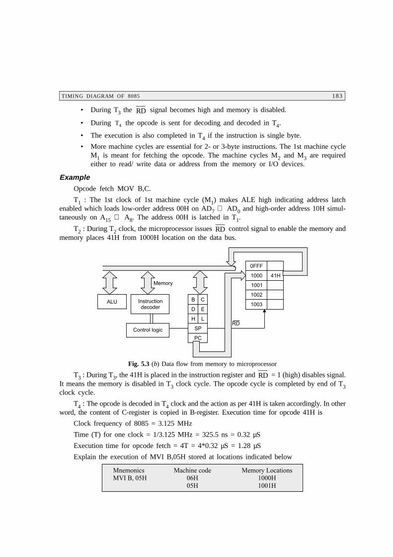
Opcode fetch MOV B,C.
T1 : The 1st clock of 1st machine cycle (M1) makes ALE high indicating address latchenabled which loads low-order address 00H on AD7 ⇔ AD0 and high-order address 10H simul-taneously on A15 ⇔ A8. The address 00H is latched in T1.
T2 : During T2 clock, the microprocessor issues RD control signal to enable the memory andmemory places 41H from 1000H location on the data bus.
Fig. 5.3 (b) Data flow from memory to microprocessor
T3 : During T3, the 41H is placed in the instruction register and RD = 1 (high) disables signal.It means the memory is disabled in T3 clock cycle. The opcode cycle is completed by end of T3clock cycle.
T4 : The opcode is decoded in T4 clock and the action as per 41H is taken accordingly. In otherword, the content of C-register is copied in B-register. Execution time for opcode 41H is
Clock frequency of 8085 = 3.125 MHz
Time (T) for one clock = 1/3.125 MHz = 325.5 ns = 0.32 µS
Execution time for opcode fetch = 4T = 4*0.32 µS = 1.28 µS
Explain the execution of MVI B,05H stored at locations indicated below
184 MICROPROCESSORS, INTERFACINGS AND APPLICATIONS
Fig. 5.3 (c) Opcode fetch (MOV B,C)
Fig. 5.3 (d) Timing diagram for MVI B,05H
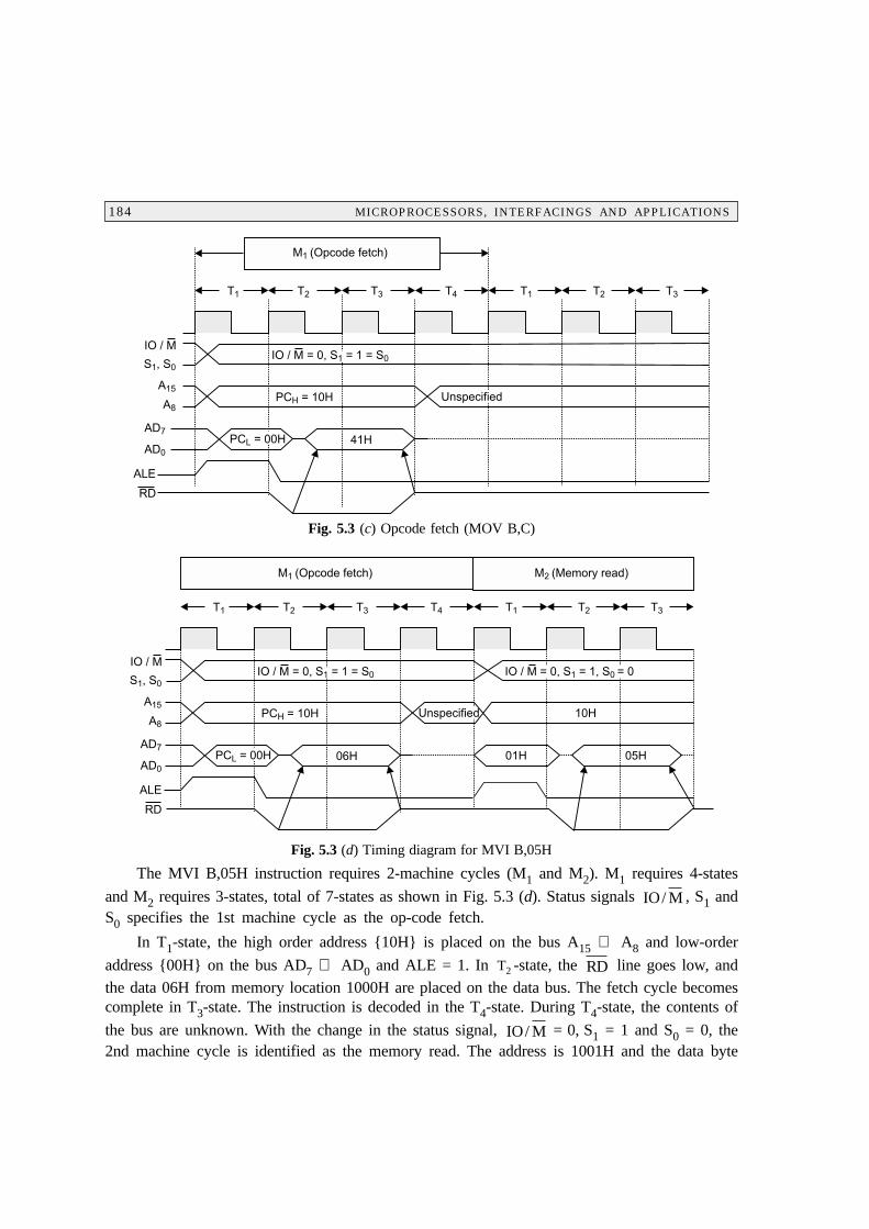
The MVI B,05H instruction requires 2-machine cycles (M1 and M2). M1 requires 4-states
and M2 requires 3-states, total of 7-states as shown in Fig. 5.3 (d). Status signals IO/ M , S1 andS0 specifies the 1st machine cycle as the op-code fetch.
In T1-state, the high order address {10H} is placed on the bus A15 ⇔ A8 and low-order
address {00H} on the bus AD7 ⇔ AD0 and ALE = 1. In 2T -state, the RD line goes low, and
the data 06H from memory location 1000H are placed on the data bus. The fetch cycle becomescomplete in T3-state. The instruction is decoded in the T4-state. During T4-state, the contents of
the bus are unknown. With the change in the status signal, IO/ M = 0, S1 = 1 and S0 = 0, the2nd machine cycle is identified as the memory read. The address is 1001H and the data byte
TIMING DIAGRAM OF 8085 185
[05H] is fetched via the data bus. Both M1 and M2 perform memory read operation, but the M1is called op-code fetch i.e., the 1st machine cycle of each instruction is identified as the opcodefetch cycle. Execution time for MBI B,05H i.e., memory read machine cycle and instruction cycleis
Mnemonic Instruction Byte Machine Cycle T-sstates
MVI B,05H Opcode Opcode Fetch 4
Immediate Data Read Immediate Data 3
7
Clock frequency of 8085 = 3.125 MHz
Time ( T ) for one clock = 1/3.125 MHz = 0.32 µS
Time for Memory Read = 3T = 3*0.320 µS = 0.96 µS
Total Execution time for Instruction = 7T = 7*0.320 µS = 2.24 µS
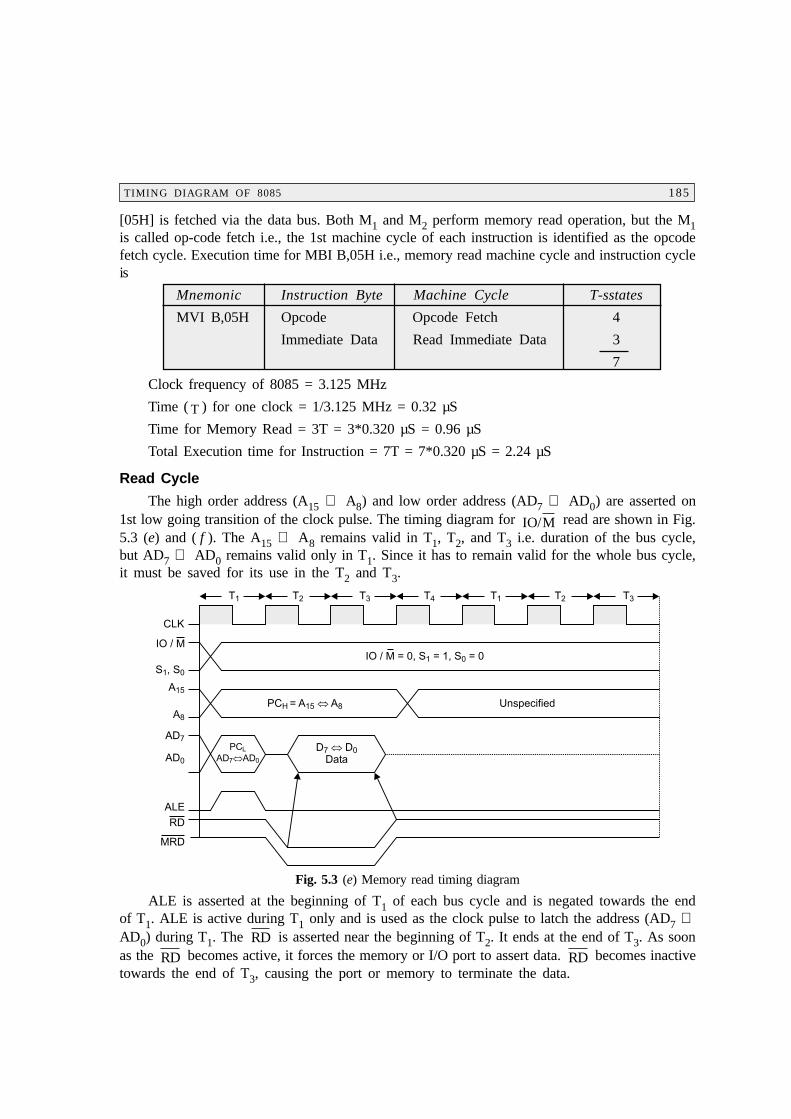
Read Cycle
The high order address (A15 ⇔ A8) and low order address (AD7 ⇔ AD0) are asserted on1st low going transition of the clock pulse. The timing diagram for IO/M read are shown in Fig.5.3 (e) and ( f ). The A15 ⇔ A8 remains valid in T1, T2, and T3 i.e. duration of the bus cycle,but AD7 ⇔ AD0 remains valid only in T1. Since it has to remain valid for the whole bus cycle,it must be saved for its use in the T2 and T3.
Fig. 5.3 (e) Memory read timing diagram
ALE is asserted at the beginning of T1 of each bus cycle and is negated towards the endof T1. ALE is active during T1 only and is used as the clock pulse to latch the address (AD7 ⇔AD0) during T1. The RD is asserted near the beginning of T2. It ends at the end of T3. As soonas the RD becomes active, it forces the memory or I/O port to assert data. RD becomes inactivetowards the end of T3, causing the port or memory to terminate the data.
186 MICROPROCESSORS, INTERFACINGS AND APPLICATIONS
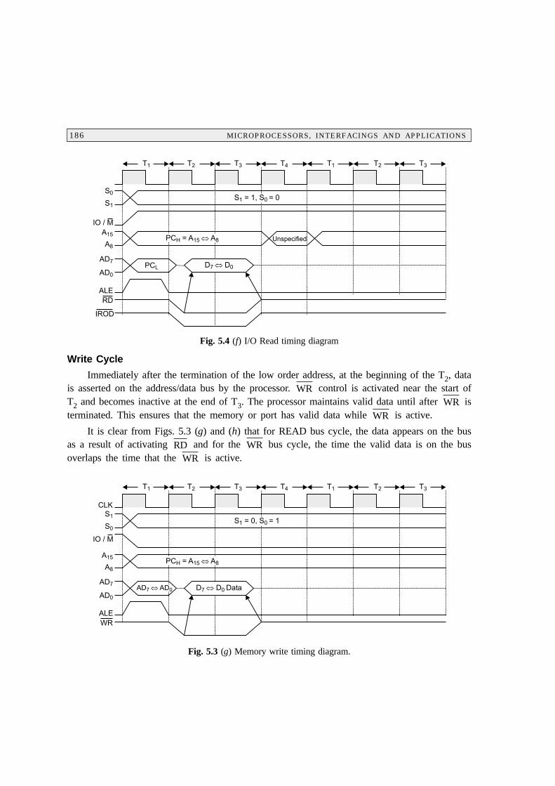
Fig. 5.4 (f) I/O Read timing diagram
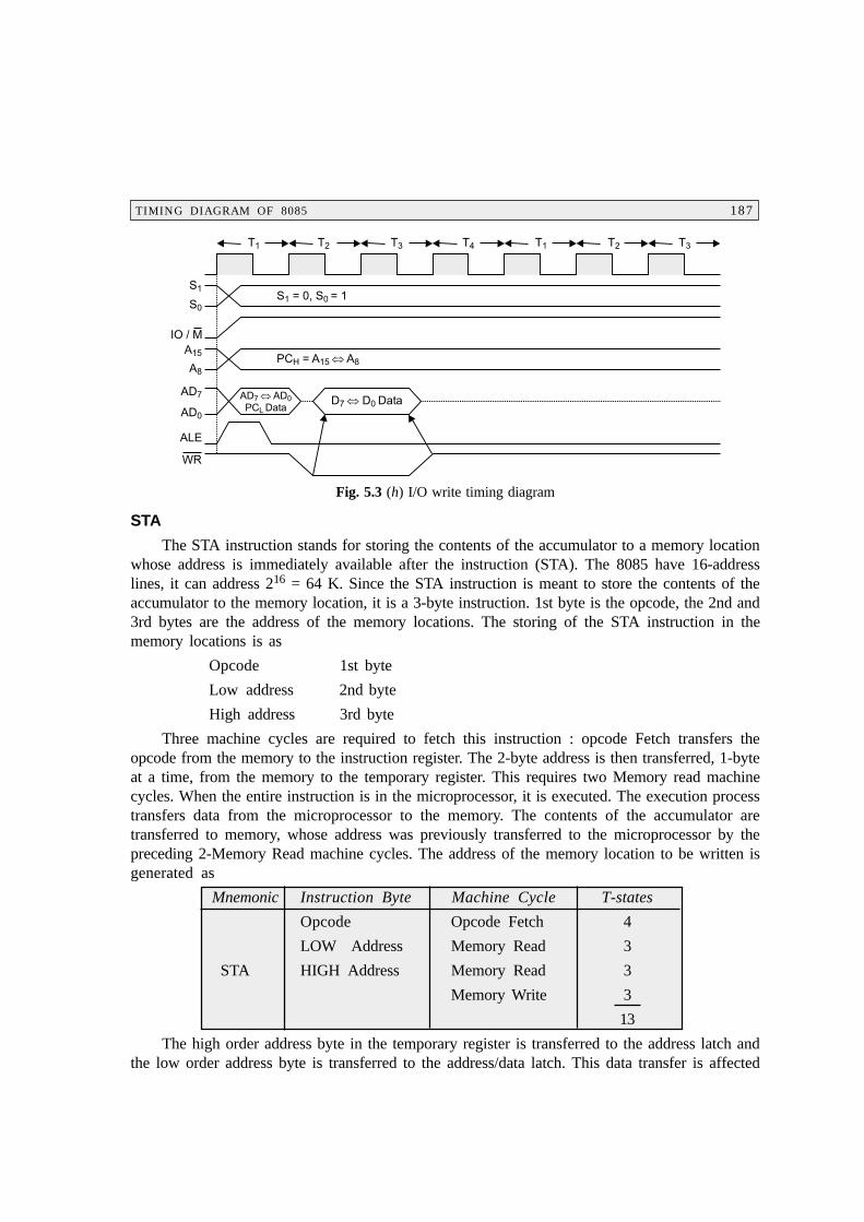
Write Cycle
Immediately after the termination of the low order address, at the beginning of the T2, datais asserted on the address/data bus by the processor. WR control is activated near the start ofT2 and becomes inactive at the end of T3. The processor maintains valid data until after WR isterminated. This ensures that the memory or port has valid data while WR is active.
It is clear from Figs. 5.3 (g) and (h) that for READ bus cycle, the data appears on the busas a result of activating RD and for the WR bus cycle, the time the valid data is on the busoverlaps the time that the WR is active.
Fig. 5.3 (g) Memory write timing diagram.
TIMING DIAGRAM OF 8085 187
Fig. 5.3 (h) I/O write timing diagram
STA
The STA instruction stands for storing the contents of the accumulator to a memory locationwhose address is immediately available after the instruction (STA). The 8085 have 16-addresslines, it can address 216 = 64 K. Since the STA instruction is meant to store the contents of theaccumulator to the memory location, it is a 3-byte instruction. 1st byte is the opcode, the 2nd and3rd bytes are the address of the memory locations. The storing of the STA instruction in thememory locations is as
Opcode 1st byte
Low address 2nd byte
High address 3rd byte
Three machine cycles are required to fetch this instruction : opcode Fetch transfers theopcode from the memory to the instruction register. The 2-byte address is then transferred, 1-byteat a time, from the memory to the temporary register. This requires two Memory read machinecycles. When the entire instruction is in the microprocessor, it is executed. The execution processtransfers data from the microprocessor to the memory. The contents of the accumulator aretransferred to memory, whose address was previously transferred to the microprocessor by thepreceding 2-Memory Read machine cycles. The address of the memory location to be written isgenerated as
Mnemonic Instruction Byte Machine Cycle T-states
Opcode Opcode Fetch 4
LOW Address Memory Read 3
STA HIGH Address Memory Read 3
Memory Write 3
13
The high order address byte in the temporary register is transferred to the address latch andthe low order address byte is transferred to the address/data latch. This data transfer is affected
188 MICROPROCESSORS, INTERFACINGS AND APPLICATIONS
by a Memory Write machine cycle. Thus 3-byte STA instruction has four machine cycles in itsinstruction cycle.
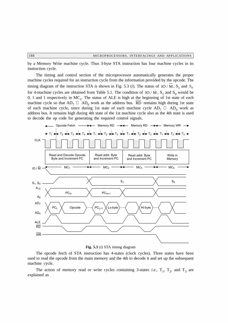
The timing and control section of the microprocessor automatically generates the propermachine cycles required for an instruction cycle from the information provided by the opcode. The
timing diagram of the instruction STA is shown in Fig. 5.3 (i). The status of IO / M , S1 and 0S
for 4-machine cycles are obtained from Table 5.1. The condition of IO / M , S1 and S0 would be0, 1 and 1 respectively in MC1. The status of ALE is high at the beginning of 1st state of eachmachine cycle so that AD7 ⇔ AD0 work as the address bus. RD remains high during 1st stateof each machine cycle, since during 1st state of each machine cycle AD7 ⇔ AD0 work asaddress bus. It remains high during 4th state of the 1st machine cycle also as the 4th state is usedto decode the op code for generating the required control signals.
Fig. 5.3 (i) STA timing diagram
The opcode fetch of STA instruction has 4-states (clock cycles). Three states have beenused to read the opcode from the main memory and the 4th to decode it and set up the subsequentmachine cycle.
The action of memory read or write cycles containing 3-states i.e., T1, T2, and T3 areexplained as
TIMING DIAGRAM OF 8085 189
T1 : During this period the address and control signals for the memory access are set up.
T2 : The µP checks up the READY and HOLD control lines. If READY = 0, indicating aslow memory device, the µP enters in the wait state until READY = 1, indicating DMA request,then only the µP floats the data transfer lines and enters into wait until HOLD = 0.
T3 : In memory read cycles the µP transfers a byte from the data bus to an internal registerand in memory write cycle the µP transfers a byte from an internal register to the data bus.
Thus STA instruction requires 4-machine cycles containing 13-states (clock cycles). With atypical clock of 3 MHz (= 330 ns), the STA instruction requires 13*330 ns = 4.29 ms for itsexecution.
REVIEW QUESTIONS
1. Calculate the execution time required for executing the instructions with the system frequencyof
3 MHz.
MOV A,B
MOV C,D
MOV A,M
MVI A,05H
MVI B,05H
2. With relevant diagram, explain the role of timing and control unit in the operation of microproc-essors.
3. Define (a) Instruction cycle, (b) Machine cycle, (c) Clock cycle.
4. Draw and explain the timing diagram for the memory read instruction.
5. Draw and explain the timing diagram for the I/O write instruction.


![STUDY & EVALUATION SCHEME Diploma in …...Size, The 8085 Microprocessor Unit, Architecture & Description. UNIT-II [8] Pin Diagram of 8085, Addressing Modes of 8085, Data Transfer](https://static.fdocuments.in/doc/165x107/5f7989d5625c5716621e9faf/study-evaluation-scheme-diploma-in-size-the-8085-microprocessor-unit.jpg)


![Scanned by CamScanner - CollegeSpacetest.collegespace.in/Academia... · Q 2 a) Draw the timing diagram for RET instruction. 14] b) The 8085 microprocessor executes program given below,](https://static.fdocuments.in/doc/165x107/5ac87d607f8b9a51678c5044/scanned-by-camscanner-2-a-draw-the-timing-diagram-for-ret-instruction-14-b.jpg)