Linear Voltage Regulator LDO, Ultra Low Noise, High PSRR ...
22
© Semiconductor Components Industries, LLC, 2013 October, 2019 − Rev. 3 1 Publication Order Number: NCV8570B/D NCV8570B Linear Voltage Regulator - LDO, Ultra Low Noise, High PSRR 200 mA The NCV8570B is a 200 mA Low Dropout, Linear Voltage Regulator with ultra low noise characteristics. It’s low noise combined with high Power Supply Rejection Ratio (PSRR) make it especially suited for use in RF, audio or imaging applications. The device is manufactured in an advanced BiCMOS process to provide a powerful combination of low noise and excellent dynamic performance but with very low ground current consumption at full loads. The NCV8570B is stable with small, low value capacitors allowing designers to minimise the total PCB space occupied by the solution. The device is packaged in a small 2x2.2mm DFN6 package as well as in a TSOP-5 package. Features • Ultra Low Noise (typ. 10 mVrms @ V OUT = 1.8 V) • Very High PSRR (typ. 82 dB @ 1 kHz) • Excellent Line and Load Regulation • Stable with Ceramic Output Capacitors as low as 1 mF • Very Low Ground Current (typ. 75 mA @ I OUT = 200 mA) • Low Sleep Mode Current (max. 1 mA) • Active Discharge Circuit • Current Limit and Thermal Shutdown Protection • Output Voltage Options: ♦ 1.8 V, 2.5 V, 2.8 V, 3.0 V, 3.3 V ♦ Contact Factory for Other Voltage Options • NCV Prefix for Automotive and Other Applications Requiring Unique Site and Control Change Requirements; AEC−Q100 Qualified and PPAP Capable • These are Pb−Free Devices Applications • Satellite and HD Radio • Portable/Built−in DVD Entertainment Systems • Noise Sensitive Applications (RF, Video, Audio) • GPS Systems • Camera for Lane Change Detection and Reverse View NCV8570B IN EN OUT BYP GND ON OFF 3 1 2, 5, EPAD 4 6 Figure 1. NCV8570B Typical Application Schematic C OUT 1 mF C noise 10 nF C IN 1 mF V IN V OUT DFN6 2x2.2 http://onsemi.com See detailed ordering, marking and shipping information in the package dimensions section on page 18 of this data sheet. ORDERING INFORMATION DFN6 MN SUFFIX CASE 506BA MARKING DIAGRAMS PIN CONNECTIONS XX = Specific Device Code M = Date Code G = Pb−Free Package* (*Note: Microdot may be in either location) DFN6 (Top View) 1 2 3 6 5 4 EN GND IN BYP GND OUT XX MG G 1 TSOP−5 SN SUFFIX CASE 483 1 5 XXXAYWG G XXX = Specific Device Code A = Assembly Location Y = Year W = Work Week G = Pb−Free Package* (*Note: Microdot may be in either location) 1 5 IN GND EN OUT BYP TSOP−5 (Top View)
Transcript of Linear Voltage Regulator LDO, Ultra Low Noise, High PSRR ...

© Semiconductor Components Industries, LLC, 2013
October, 2019 − Rev. 31 Publication Order Number:
NCV8570B/D
NCV8570B
Linear Voltage Regulator -LDO, Ultra Low Noise, HighPSRR
200 mA
The NCV8570B is a 200 mA Low Dropout, Linear VoltageRegulator with ultra low noise characteristics. It’s low noise combinedwith high Power Supply Rejection Ratio (PSRR) make it especiallysuited for use in RF, audio or imaging applications. The device ismanufactured in an advanced BiCMOS process to provide a powerfulcombination of low noise and excellent dynamic performance but withvery low ground current consumption at full loads.
The NCV8570B is stable with small, low value capacitors allowingdesigners to minimise the total PCB space occupied by the solution.The device is packaged in a small 2x2.2mm DFN6 package as well asin a TSOP-5 package.Features• Ultra Low Noise (typ. 10 �Vrms @ VOUT = 1.8 V)
• Very High PSRR (typ. 82 dB @ 1 kHz)
• Excellent Line and Load Regulation
• Stable with Ceramic Output Capacitors as low as 1 �F
• Very Low Ground Current (typ. 75 �A @ IOUT = 200 mA)
• Low Sleep Mode Current (max. 1 �A)
• Active Discharge Circuit
• Current Limit and Thermal Shutdown Protection
• Output Voltage Options:♦ 1.8 V, 2.5 V, 2.8 V, 3.0 V, 3.3 V♦ Contact Factory for Other Voltage Options
• NCV Prefix for Automotive and Other Applications RequiringUnique Site and Control Change Requirements; AEC−Q100Qualified and PPAP Capable
• These are Pb−Free DevicesApplications• Satellite and HD Radio
• Portable/Built−in DVD Entertainment Systems
• Noise Sensitive Applications (RF, Video, Audio)
• GPS Systems
• Camera for Lane Change Detection and Reverse View
NCV8570B
IN
EN
OUT
BYP
GNDON
OFF
3
1
2, 5, EPAD
4
6
Figure 1. NCV8570B Typical Application Schematic
COUT1 �F
Cnoise10 nF
CIN1 �F
VIN VOUT
DFN6 2x2.2
http://onsemi.com
See detailed ordering, marking and shipping information in thepackage dimensions section on page 18 of this data sheet.
ORDERING INFORMATION
DFN6MN SUFFIX
CASE 506BA
MARKING DIAGRAMS
PIN CONNECTIONS
XX = Specific Device CodeM = Date Code� = Pb−Free Package*
(*Note: Microdot may be in either location)
DFN6(Top View)
1
2
3
6
5
4
EN
GND
IN
BYP
GND
OUT
XX M�
�
1
TSOP−5SN SUFFIXCASE 483
1
5
XXXAYW�
�
XXX = Specific Device CodeA = Assembly LocationY = YearW = Work Week� = Pb−Free Package*
(*Note: Microdot may be in either location)
1 5IN
GND
EN
OUT
BYP
TSOP−5(Top View)
NCV8570B
http://onsemi.com2
RPD
RDIS
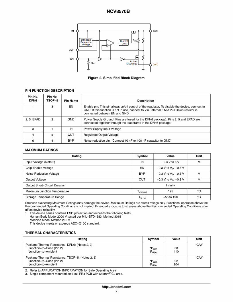
Figure 2. Simplified Block Diagram
PIN FUNCTION DESCRIPTION
Pin No.DFN6
Pin No.TSOP−5 Pin Name Description
1 3 EN Enable pin: This pin allows on/off control of the regulator. To disable the device, connect toGND. If this function is not in use, connect to Vin. Internal 5 M� Pull Down resistor isconnected between EN and GND.
2, 5, EPAD 2 GND Power Supply Ground (Pins are fused for the DFN6 package). Pins 2, 5 and EPAD areconnected together through the lead frame in the DFN6 package.
3 1 IN Power Supply Input Voltage
4 5 OUT Regulated Output Voltage
6 4 BYP Noise reduction pin. (Connect 10 nF or 100 nF capacitor to GND)
MAXIMUM RATINGS
Rating Symbol Value Unit
Input Voltage (Note 2) IN −0.3 V to 6 V V
Chip Enable Voltage EN −0.3 V to VIN +0.3 V
Noise Reduction Voltage BYP −0.3 V to VIN +0.3 V V
Output Voltage OUT −0.3 V to VIN +0.3 V V
Output Short−Circuit Duration Infinity
Maximum Junction Temperature TJ(max) 125 °C
Storage Temperature Range TSTG −55 to 150 °C
Stresses exceeding Maximum Ratings may damage the device. Maximum Ratings are stress ratings only. Functional operation above theRecommended Operating Conditions is not implied. Extended exposure to stresses above the Recommended Operating Conditions mayaffect device reliability.1. This device series contains ESD protection and exceeds the following tests:
Human Body Model 2000 V tested per MIL−STD−883, Method 3015Machine Model Method 200 VThis device meets or exceeds AEC−Q100 standard.
THERMAL CHARACTERISTICS
Rating Symbol Value Unit
Package Thermal Resistance, DFN6: (Notes 2, 3)Junction−to−Case (Pin 2)Junction−to−Ambient
�JL2R�JA
38110
°C/W
Package Thermal Resistance, TSOP−5: (Notes 2, 3)Junction−to−Case (Pin 2)Junction−to−Ambient
�JL2R�JA
92204
°C/W
2. Refer to APPLICATION INFORMATION for Safe Operating Area3. Single component mounted on 1 oz, FR4 PCB with 645mm2 Cu area.

NCV8570B
http://onsemi.com3
ELECTRICAL CHARACTERISTICS (VIN = VOUT + 0.5 V or 2.5 V (whichever is greater), VEN = 1.2 V, CIN = COUT = 1 �F, Cnoise = 10 nF, IOUT = 1 mA, TJ = −40°C to 125°C,unless otherwise specified) (Note 4)
Parameter Test Conditions Symbol Min Typ Max Unit
REGULATOR OUTPUT
Input Voltage Range VIN 2.5 − 5.5 V
Output Voltage 1.8 V2.5 V2.8 V3.0 V3.3 V
VIN = (VOUT + 0.5 V) to 5.5 VIOUT = 1 mA to 200 mA
VOUT 1.7552.43752.7302.9253.2175(−2.5%)
−−−−−
1.8452.56252.8703.0753.3825(+2.5%)
V
Power Supply Ripple Rejection VIN = VOUT +1.0 V,IOUT = 1 mA to 150 mA
f = 120 Hzf = 1 kHzf = 10 kHz
PSRR −−−
808263
−−−
dB
Line Regulation VIN = (VOUT +0.5 V) to 5.5 V, IOUT = 1 mA �VOUT / �VIN −0.1 − 0.1 %/V
Load Regulation IOUT = 1 mA to 200 mA �VOUT / �IOUT − 0.2 5.0 mV
Output Noise Voltage VOUT = 1.8 V,f = 10 Hz to 100 kHz,IOUT = 1 mA to 150 mA
Cnoise = 100 nFCnoise = 10 nF
VN −−
1015
−−
�VRMS
Output Current Limit VOUT = VOUT(NOM) – 0.1 V ILIM 200 310 470 mA
Output Short Circuit Current VOUT = 0V ISC 205 320 490 mA
Dropout Voltage (Note 5) IOUT= 150 mA VOUT(NOM) = 2.5 VVOUT(NOM) = 2.8 VVOUT(NOM) = 3.0 VVOUT(NOM) = 3.3 V
VDO −−−−
100908580
180165150145
mV
Dropout Voltage (Note 5) IOUT= 200 mA VOUT(NOM) = 2.5 VVOUT(NOM) = 2.8 VVOUT(NOM) = 3.0 VVOUT(NOM) = 3.3 V
VDO −−−−
140120115110
230205190185
mV
GENERAL
Ground Current IOUT = 1 mAIOUT = 200 mA
IGND −−
7075
110130
�A
Disable Current VEN = 0 V IDIS − 0.1 1.0 �A
Thermal Shutdown Shutdown, Temperature Increasing TSDU − 150 − °C
Reset, Temperature Decreasing TSDD − 135 − °C
OUTPUT ENABLE
Enable Threshold LowHigh
Vth(EN) −1.2
−−
0.4−
V
Internal Pull−Down Resistance(Note 6)
RPD(EN) 2.5 5.0 10 M�
TIMING
Turn−On Time IOUT = 10 mA, VOUT =0.975 VOUT(NOM)
Cnoise = 10 nFCnoise = 100 nF
tON −−
0.44.0
−−
ms
Turn−Off Time Cnoise = 10nF/100nF,VOUT = 0.1 VOUT(NOM)
IOUT = 1 mAIOUT = 10 mA
tOFF −−
2.00.6
−−
ms
4. Performance guaranteed over the indicated operating temperature range by design and/or characterization tested at TJ = TA = 25°C. Lowduty cycle pulse techniques are used during testing to maintain the junction temperature as close to ambient as possible.
5. Measured when the output voltage falls 100 mV below the nominal output voltage (nominal output voltage is the voltage at the output meas-ured under the condition VIN = VOUT + 0.5 V). In the case of devices having the nominal output voltage VOUT = 1.8 V the minimum inputto output voltage differential is given by the VIN(MIN) = 2.5 V.
6. Expected to disable the device when EN pin is floating.

NCV8570B
http://onsemi.com4
TYPICAL CHARACTERISTICS
1.764
1.776
1.788
1.800
1.812
1.824
1.836
Figure 3. Output Voltage vs. JunctionTemperature, VOUT = 1.8 V
TJ, JUNCTION TEMPERATURE (°C)
Vou
t, O
UT
PU
T V
OLT
AG
E (
V)
VIN = 2.5 V,CIN = COUT = 1 �F,Cnoise = 10 nF
−40 −20 0 20 40 60 80 100 120
2.7440
2.7627
2.7813
2.8000
2.8187
2.8373
2.8560
Vou
t, O
UT
PU
T V
OLT
AG
E (
V)
Figure 4. Output Voltage vs. JunctionTemperature, VOUT = 2.8 V
TJ, JUNCTION TEMPERATURE (°C)
VIN = 3.3 V,CIN = COUT = 1 �F,Cnoise = 10 nF
−40 −20 0 20 40 60 80 100 120
2.94
2.96
2.98
3.00
3.02
3.04
3.06
Vou
t, O
UT
PU
T V
OLT
AG
E (
V)
Figure 5. Output Voltage vs. JunctionTemperature, VOUT = 3.0 V
TJ, JUNCTION TEMPERATURE (°C)
VIN = 3.5 V,CIN = COUT = 1 �F,Cnoise = 10 nF
−40 −20 0 20 40 60 80 100 120

NCV8570B
http://onsemi.com5
TYPICAL CHARACTERISTICS
3.2340
3.2560
3.2780
3.3000
3.3220
3.3440
3.3660
Vou
t, O
UT
PU
T V
OLT
AG
E (
V)
Figure 6. Output Voltage vs. JunctionTemperature, VOUT = 3.3 V
TJ, JUNCTION TEMPERATURE (°C)
VIN = 3.8 V,CIN = COUT = 1 �F,Cnoise = 10 nF
−40 −20 0 20 40 60 80 100 1200
30
60
90
120
150
180
0 40 80 120 160 200
VD
O, D
RO
PO
UT
VO
LTA
GE
(m
V)
IOUT, OUTPUT CURRENT (mA)Figure 7. Dropout Voltage vs. Output Current,
VOUT = 2.8 V
CIN = COUT = 1 �F,Cnoise = 10 nF
TJ = 125°C
TJ = 25°C
TJ = −40°C
0
30
60
90
120
150
180
0 40 80 120 160 200
VD
O, D
RO
PO
UT
VO
LTA
GE
(m
V)
IOUT, OUTPUT CURRENT (mA)
Figure 8. Dropout Voltage vs. Output Current,VOUT = 3.0 V
CIN = COUT = 1 �F,Cnoise = 10 nF
TJ = 125°C
TJ = 25°C
TJ = −40°C
0
30
60
90
120
150
180
0 40 80 120 160 200
VD
O, D
RO
PO
UT
VO
LTA
GE
(m
V)
IOUT, OUTPUT CURRENT (mA)
Figure 9. Dropout Voltage vs. Output Current,VOUT = 3.3 V
CIN = COUT = 1 �F,Cnoise = 10 nF
TJ = 125°C
TJ = 25°C
TJ = −40°C

NCV8570B
http://onsemi.com6
TYPICAL CHARACTERISTICS
0
10
20
30
40
50
60
70
80
90
100
10 100 1k 10k 100k 1M
Figure 10. PSRR vs. Frequency, 1.8 V OutputVoltage Option, COUT = 1 �F, Cnoise = 10 nF
FREQUENCY (Hz)
PS
RR
(dB
)
TA = 25°C,Cnoise = 10 nF,COUT = 1 �F,VOUT = 1.8 V,VIN = 3.0 VDC ± 50 mVAC
IOUT = 10 mA
IOUT = 150 mA
IOUT = 200 mA
0
10
20
30
40
50
60
70
80
90
100
110
10 100 1k 10k 100k 1M
Figure 11. PSRR vs. Frequency, 1.8 V OutputVoltage Option, COUT = 1�F, Cnoise = 100nF
FREQUENCY (Hz)
PS
RR
(dB
)
TA = 25°C,Cnoise = 100 nF,COUT = 1 �F,VOUT = 1.8 V,VIN = 3.0 VDC ± 50 mVAC
IOUT = 10 mA
IOUT = 150 mA
IOUT = 200 mA
0
10
20
30
40
50
60
70
80
90
100
FREQUENCY (Hz)
PS
RR
(dB
)
10 100 1k 10k 100k 1M
Figure 12. PSRR vs. Frequency, 1.8 V OutputVoltage Option, COUT = 4.7 �F, Cnoise = 10 nF
TA = 25°C,Cnoise = 10 nF,COUT = 4.7 �F,VOUT = 1.8 V,VIN = 3.0 VDC ± 50 mVAC
IOUT = 10 mA
IOUT = 150 mA
IOUT = 200 mA
0
10
20
30
40
50
60
70
80
90
100
110
120
10 100 1k 10k 100k 1MFREQUENCY (Hz)
PS
RR
(dB
)
Figure 13. PSRR vs. Frequency, 1.8V OutputVoltage Option, COUT = 4.7�F, Cnoise = 100nF
TA = 25°C,Cnoise = 100 nF,COUT = 4.7 �F,VOUT = 1.8 V,VIN = 3.0 VDC ± 50 mVAC
IOUT = 10 mA
IOUT = 150 mA
IOUT = 200 mA
0
10
20
30
40
50
60
70
80
90
100
110
FREQUENCY (Hz)
PS
RR
(dB
)
10 100 1k 10k 100k 1M
Figure 14. PSRR vs. Frequency, 2.8 V OutputVoltage Option, COUT = 1 �F, Cnoise = 10 nF
TA = 25°C,Cnoise = 10 nF,COUT = 1 �F,VOUT = 2.8 V,VIN = 3.3 VDC ± 50 mVAC
IOUT = 10 mA
IOUT = 150 mA
IOUT = 200 mA
0
10
20
30
40
50
60
70
80
90
100
110
10 100 1k 10k 100k 1MFREQUENCY (Hz)
PS
RR
(dB
)
Figure 15. PSRR vs. Frequency, 2.8 V OutputVoltage Option, COUT = 1 �F, Cnoise = 100 nF
IOUT = 10 mA
IOUT = 150 mA
IOUT = 200 mA
TA = 25°C,Cnoise = 100 nF,COUT = 1 �F,VOUT = 2.8 V,VIN = 3.3 VDC ± 50 mVAC

NCV8570B
http://onsemi.com7
TYPICAL CHARACTERISTICS
0
10
20
30
40
50
60
70
80
90
100
110
Figure 16. PSRR vs. Frequency, 2.8 V OutputVoltage Option, COUT = 4.7 �F, Cnoise = 10 nF
FREQUENCY (Hz)
PS
RR
(dB
)
10 100 1k 10k 100k 1M
IOUT = 10 mA
IOUT = 150 mA
IOUT = 200 mA
TA = 25°C,Cnoise = 10 nF,COUT = 4.7 �F,VOUT = 2.8 V,VIN = 3.3 VDC ± 50 mVAC
0
10
20
30
40
50
60
70
80
90
100
110
Figure 17. PSRR vs. Frequency, 2.8 V OutputVoltage Option, COUT = 4.7 �F, Cnoise = 100 nF
FREQUENCY (Hz)
PS
RR
(dB
)
10 100 1k 10k 100k 1M
IOUT = 10 mA
IOUT = 150 mA
IOUT = 200 mA
TA = 25°C,Cnoise = 100 nF,COUT = 4.7 �F,VOUT = 2.8 V,VIN = 3.3 VDC ± 50 mVAC
0.01
0.10
1.0
10
Figure 18. Output Noise vs. Frequency, COUT =1 �F, Cnoise = 10 nF, IOUT = 50 mA
FREQUENCY (Hz)
10 100 1k 10k 100k 1M
OU
TP
UT
VO
LTA
GE
NO
ISE
(�V
/√H
Z)
IOUT = 50 mA,COUT = 1 �F,Cnoise = 10 nFVIN = VOUT = +0.5 V or2.5 V, whichever is higher
VOUT = 1.8 V10 Hz − 100 kHz IntegralNoise: Vn = 14.9 �Vrms
VOUT = 3.3 V10 Hz − 100 kHz IntegralNoise: Vn = 25.3 �Vrms
VOUT = 2.8 V10 Hz − 100 kHz IntegralNoise: Vn = 22.6 �Vrms
0.01
0.10
1.0
10
Figure 19. Output Noise vs. Frequency, COUT =1 �F, Cnoise = 100 nF, IOUT = 50 mA
FREQUENCY (Hz)
10 100 1k 10k 100k 1M
OU
TP
UT
VO
LTA
GE
NO
ISE
(�V
/√H
Z) IOUT = 50 mA,
COUT = 1 �F,Cnoise = 100 nFVIN = VOUT = +0.5 V or2.5 V, whichever is higher
VOUT = 2.8 V10 Hz − 100 kHz IntegralNoise: Vn = 11.7 �Vrms
VOUT = 3.3 V10 Hz − 100 kHz IntegralNoise: Vn = 11.9 �Vrms
VOUT = 1.8 V10 Hz − 100 kHz Integral
Noise: Vn = 9.4 �Vrms
0.01
0.10
1.0
10
FREQUENCY (Hz)
OU
TP
UT
VO
LTA
GE
NO
ISE
(�V
/√H
Z)
Figure 20. Output Noise vs. Frequency, COUT =1 �F, Cnoise = 10 nF, IOUT = 200 mA
10 100 1k 10k 100k 1M
IOUT = 200 mA,COUT = 1 �F,Cnoise = 10 nFVIN = VOUT = +0.5 V or2.5 V, whichever is higher
VOUT = 1.8 V10 Hz − 100 kHz Integral
Noise: Vn = 15 �Vrms
VOUT = 3.3 V10 Hz − 100 kHz IntegralNoise: Vn = 22.85 �Vrms
VOUT = 2.8 V10 Hz − 100 kHz IntegralNoise: Vn = 22.7 �Vrms
0.01
0.10
1.0
10
FREQUENCY (Hz)10 100 1k 10k 100k 1M
OU
TP
UT
VO
LTA
GE
NO
ISE
(�V
/√H
Z)
Figure 21. Output Noise vs. Frequency, COUT =1 �F, Cnoise = 100 nF, IOUT = 200 mA
VOUT = 1.8 V10 Hz − 100 kHz Integral
Noise: Vn = 9.5 �Vrms
VOUT = 3.3 V10 Hz − 100 kHz Integral
Noise: Vn = 12 �Vrms
VOUT = 2.8 V10 Hz − 100 kHz IntegralNoise: Vn = 11.7 �Vrms
IOUT = 200 mA,COUT = 1 �F,Cnoise = 100 nFVIN = VOUT = +0.5 V or2.5 V, whichever is higher

NCV8570B
http://onsemi.com8
TYPICAL CHARACTERISTICS
5
10
15
20
25
30
35
0 50 100 150 200 250 300 350 400 450 500
Figure 22. Output Noise vs. Noise BypassCapacitance, COUT = 1 �F, VOUT = 3.3 V, IOUT =
200 mA
Cnoise, NOISE BYPASS CAPACITOR (nF)
10 H
Z to
100
kH
z R
MS
OU
TP
UT
NO
ISE
(�V
rms)
TA = 25°C,COUT = 1 �F,VOUT = 3.3 V,IOUT = 200 mAVIN = 3.8 V
Figure 23. Output Noise vs. OutputCapacitance, Cnoise = 100 nF, VOUT = 3.3 V,
IOUT = 200 mA
0
2
4
6
8
10
12
14
16
18
20
1 3 5 7 9 11 13 15 17 19 21
10 H
Z to
100
kH
z R
MS
OU
TP
UT
NO
ISE
(�V
rms)
COUT, OUTPUT CAPACITOR (�F)
TA = 25°C,Cnoise = 100 nF,VOUT = 3.3 V,IOUT = 200 mAVIN = 3.8 V
10
12
14
16
18
20
22
24
26
28
30
0 25 50 75 100 125 150 175 200
10 H
Z to
100
kH
z R
MS
OU
TP
UT
NO
ISE
(�V
rms)
IOUT, OUTPUT CURRENT (mA)
Figure 24. Output Noise vs. Load Current,Cnoise = 10 nF, COUT = 1 �F
VOUT = 3.3 V
VOUT = 2.8 V
VOUT = 1.8 V
TA = 25°C, Cnoise = 10 nF, COUT = 1 �F,VIN = VOUT + 0.5 V or 2.5 V, whichever is higher
5
6
7
8
9
10
11
12
13
14
15
0 25 50 75 100 125 150 175 200IOUT, OUTPUT CURRENT (mA)
Figure 25. Output Noise vs. Load Current,Cnoise = 100 nF, COUT = 1 �F
10 H
Z to
100
kH
z R
MS
OU
TP
UT
NO
ISE
(�V
rms)
TA = 25°C, Cnoise = 100 nF, COUT = 1 �F,VIN = VOUT + 0.5 V or 2.5 V, whichever is higher
VOUT = 3.3 V
VOUT = 2.8 V
VOUT = 1.8 V
1.60
1.65
1.70
1.75
1.80
1.85
0 40 80 120 160 200 240 280 320 360 400
0
100
200
300
VO
UT,
OU
TP
UT
VO
LTA
GE
(V
)
t, TIME (�s)
Figure 26. Load Transient Response, VOUT =1.8 V, COUT = 4.7 �F, Cnoise = 100 nF
I OU
T, O
UT
PU
T C
UR
RE
NT
(m
A)
1 mA200 mA
COUT = 4.7 �F, VIN = 2.5 V, Cnoise = 100 nF,dIOUT/dt = 200 mA / 1 �s

NCV8570B
http://onsemi.com9
TYPICAL CHARACTERISTICS
1.60
1.65
1.70
1.75
1.80
1.85
1.90
0 40 80 120 160 200 240 280 320 360 400
0
100
200
300
VO
UT,
OU
TP
UT
VO
LTA
GE
(V
)
t, TIME (�s)
Figure 27. Load Transient Response, VOUT =1.8 V, COUT = 1 �F, Cnoise = 100 nF
I OU
T, O
UT
PU
T C
UR
RE
NT
(m
A)
1 mA200 mA
VO
UT,
OU
TP
UT
VO
LTA
GE
(V
)
t, TIME (�s)
Figure 28. Load Transient Response, VOUT =3.3 V, COUT = 4.7 �F, Cnoise = 100 nF
I OU
T, O
UT
PU
T C
UR
RE
NT
(m
A)
1 mA
200 mA
3.10
3.15
3.20
3.25
3.30
3.35
3.40
0 40 80 120 160 200 240 280 320 360 400
0
100
200
300
VO
UT,
OU
TP
UT
VO
LTA
GE
(V
)
t, TIME (�s)Figure 29. Load Transient Response, VOUT =
3.3 V, COUT = 1 �F, Cnoise = 100 nF
I OU
T, O
UT
PU
T C
UR
RE
NT
(m
A)
1 mA200 mA
3.10
3.15
3.20
3.25
3.30
3.35
3.40
0 40 80 120 160 200 240 280 320 360 400
0
100
200
300
COUT = 1 �F, VIN = 2.5 V, Cnoise = 100 nF,dIOUT/dt = 200 mA / 1 �s
COUT = 4.7 �F, VIN = 3.8 V, Cnoise = 100 nF,dIOUT/dt = 200 mA / 1 �s
COUT = 1 �F, VIN = 3.8 V, Cnoise = 100 nF,dIOUT/dt = 200 mA / 1 �s

NCV8570B
http://onsemi.com10
TYPICAL CHARACTERISTICS
1.780
1.785
1.790
1.795
1.800
1.805
1.810
0 20 40 60 80 100 120 140 160 180 200
2.5
3.0
3.5
4.0
VO
UT,
OU
TP
UT
VO
LTA
GE
(V
)
t, TIME (�s)Figure 30. Line Transient Response,
VOUT = 1.8 V, COUT = 1 �F, IOUT = 30 mA
VIN
, IN
PU
T V
OLT
AG
E (
V)
VIN = 2.5 V
VIN = 3.5 V
1.780
1.785
1.790
1.795
1.800
1.805
1.810
0 20 40 60 80 100 120 140 160 180 200
2.5
3.0
3.5
4.0
VO
UT,
OU
TP
UT
VO
LTA
GE
(V
)
t, TIME (�s)Figure 31. Line Transient Response,
VOUT = 1.8 V, COUT = 1 �F, IOUT = 200 mA
VIN
, IN
PU
T V
OLT
AG
E (
V)
VIN = 2.5 V
VIN = 3.5 V
COUT = 1 �F, VIN = 2.5 V, Cnoise = 100 nF,IOUT = 30 mA, dVIN/dt = 1 V / 1 �s
COUT = 1 �F, VIN = 2.5 V, Cnoise = 100 nF, IOUT = 200 mA,dVIN/dt = 1 V / 1 �s
2.980
2.985
2.990
2.995
3.000
3.005
3.010
0 20 40 60 80 100 120 140 160 180 200
3.5
4.0
4.5
5.0
VO
UT,
OU
TP
UT
VO
LTA
GE
(V
)
t, TIME (�s)Figure 32. Line Transient Response,
VOUT = 3.0 V, COUT = 1 �F, IOUT = 30 mA
VIN
, IN
PU
T V
OLT
AG
E (
V)
VIN = 3.5 V
VIN = 4.5 V
COUT = 1 �F, VIN = 3.5 V, Cnoise = 100 nF, IOUT = 30 mA,dVIN/dt = 1 V / 1 �s

NCV8570B
http://onsemi.com11
TYPICAL CHARACTERISTICS
2.980
2.985
2.990
2.995
3.000
3.005
3.010
0 20 40 60 80 100 120 140 160 180 200
3.5
4.0
4.5
5.0
VO
UT,
OU
TP
UT
VO
LTA
GE
(V
)
t, TIME (�s)Figure 33. Line Transient Response,
VOUT = 3.0 V, COUT = 1 �F, IOUT = 200 mA
VIN
, IN
PU
T V
OLT
AG
E (
V)
VIN = 3.5 V
VIN = 4.5 V
COUT = 1 �F, VIN = 3.5 V, Cnoise = 100 nF, IOUT = 200 mA,dVIN/dt = 1 V / 1 �s
−1.0
0.0
1.0
2.0
3.0
4.0
0 2 4 6 8 10 12 14 16
0.0
1.9
3.8
5.7
VO
UT,
OU
TP
UT
VO
LTA
GE
(V
)
t, TIME (ms)Figure 34. Turn−On Response
VOUT = 3.3 V, COUT = 1 �F, IOUT = 30 mA
VE
N, E
NA
BLE
VO
LTA
GE
(V
)VEN = 3.8 V
Cnoise = 47 nF
Cnoise = 100 nF
Cnoise = 220 nF
Cnoise = 10 nF
COUT = 1 �F,VIN = 3.8 V
VEN = 0 V
−1.0
0.0
1.0
2.0
3.0
4.0
0 2 4 6 8 10 12 14 16
0.00
1.75
3.50
5.25
VO
UT,
OU
TP
UT
VO
LTA
GE
(V
)
t, TIME (ms)Figure 35. Turn−On Response
VOUT = 3 V, COUT = 1 �F, IOUT = 30 mA
VE
N, E
NA
BLE
VO
LTA
GE
(V
)VEN = 3.5 V
VEN = 0 V
Cnoise = 47 nF
Cnoise = 220 nF
Cnoise = 10 nF
COUT = 1 �F,VIN = 3.5 V
Cnoise = 100 nF

NCV8570B
http://onsemi.com12
TYPICAL CHARACTERISTICS
−0.5
0.0
0.5
1.0
1.5
2.0
0 1 2 3 4 5 6 7 8 9 10
0
1
2
3
VO
UT,
OU
TP
UT
VO
LTA
GE
(V
)
t, TIME (ms)Figure 36. Turn−On Response
VOUT = 1.8 V, COUT = 1 �F, IOUT = 30 mA
VE
N, E
NA
BLE
VO
LTA
GE
(V
)
VEN = 2.5 V
VEN = 0 V
Cnoise = 47 nF
Cnoise = 220 nF
Cnoise = 10 nF
COUT = 1 �F,VIN = 2.5 V
Cnoise = 100 nF
−1.0
0.0
1.0
2.0
3.0
4.0
0 1 2 3 4 5 6 7 8 9 10
0.0
1.9
3.8
5.7
VO
UT,
OU
TP
UT
VO
LTA
GE
(V
)
t, TIME (ms)Figure 37. Turn−Off Response
VOUT = 3.3 V, COUT = 1 �F
VE
N, E
NA
BLE
VO
LTA
GE
(V
)
VEN = 3.8 V
VEN = 0 V
RRLOAD = 22 �
Cnoise = 10 nF,TJ = 25°C
RRLOAD = 110 �
RRLOAD = 3.3 k�
−1.0
0.0
1.0
2.0
3.0
0 1 2 3 4 5 6 7 8 9 10
0.00
1.75
3.50
5.25
VO
UT,
OU
TP
UT
VO
LTA
GE
(V
)
t, TIME (ms)Figure 38. Turn−Off Response
VOUT = 3 V, COUT = 1 �F
VE
N, E
NA
BLE
VO
LTA
GE
(V
)
VEN = 3.5 V
VEN = 0 V
Cnoise = 10 nF,TJ = 25°C
RRLOAD = 20 �
RRLOAD = 100 �
RRLOAD = 3 k�

NCV8570B
http://onsemi.com13
TYPICAL CHARACTERISTICS
−0.5
0.0
0.5
1.0
1.5
2.0
0 1 2 3 4 5 6 7 8 9 10
0
1.25
2.5
3.75
VO
UT,
OU
TP
UT
VO
LTA
GE
(V
)
t, TIME (ms)Figure 39. Turn−Off Response
VOUT = 1.8 V, COUT = 1 �F
VE
N, E
NA
BLE
VO
LTA
GE
(V
)
VEN = 2.5 V
VEN = 0 V
Cnoise = 10 nF,TJ = 25°C
RRLOAD = 12 �
RRLOAD = 60 �
RRLOAD = 1.8 k�
0
2
4
6
8
10
12
0 20 40 60 80 100 120 140 160 180 200 220 240
t ON
, TU
RN−
ON
TIM
E (
ms)
Cnoise, NOISE BYPASS CAPACITANCE (nF)Figure 40. Turn−On Time vs. Noise Bypass
Capacitance, COUT = 1 �F, IOUT = 0 mA −200 mA
VOUT = 3.3 V
VOUT = 3 V
VOUT = 1.8 V
TJ = 25°C,IOUT = 0 mA − 200 mA
−1
0
1
2
3
4
0.0 0.1 0.2 0.3 0.4 0.5 0.6 0.7 0.8 0.9 1.0
0
200
400
600
800
VO
UT,
OU
TP
UT
VO
LTA
GE
(V
)
I OU
T, O
UT
PU
T C
UR
RE
NT
(m
A)
t, TIME (ms)Figure 41. Short−Circuit Protection,
VOUT = 3 V, COUT = 1 �F, Cnoise = 100 nF
Short−Circuit
IOUT = 325 mA
VOUT = 0 V
NormalOperation
IOUT = 1 mA
VOUT = 3 V
IOUT = 1 mACnoise = 100 nF
−1.0
0
1.0
2.0
3.0
4.0
0.0 1.0 2.0 3.0 4.0 5.0 6.0 7.0 8.0 9.0 10.0
0
100
200
300
400
VO
UT,
OU
TP
UT
VO
LTA
GE
(V
)
I OU
T, O
UT
PU
T C
UR
RE
NT
(m
A)
VIN, INPUT VOLTAGE (V)
Figure 42. Short−Circuit Current vs. JunctionTemperature, VOUT = 1.8 V, 3.3 V
NormalOperation
ThermalShutdown IOUT = 200 mA
VOUT = 3 V
IOUT = 200 mACnoise = 100 nF
0.00
0.25
0.50
0.75
1.00
1.25
1.50
1.75
2.00
0 0.5 1 1.5 2 2.5 3 3.5 4 4.5 5 5.5
VO
UT,
OU
TP
UT
VO
LTA
GE
(V
)
VIN, INPUT VOLTAGE (V)
TJ = 25°C
TJ = −40°C
TJ = 125°CIOUT = 10 mACnoise = 100 nF
Figure 43. Thermal Shutdown ProtectionVOUT = 3 V, Cnoise = 100 nF, COUT = 1 �F
Figure 44. Output Voltage vs. Input Voltage,VOUT = 1.8 V, COUT = 1 �F
250
267
283
300
317
333
350
TJ, JUNCTION TEMPERATURE (°C)
I SC
, SH
OR
T−
CIR
CU
IT C
UR
RE
NT
(m
A)
0.0 0.1 0.2 0.3 0.4 0.5 0.6 0.7 0.8 0.9 1.0 −40 −20 0 20 40 60 80 100 120
VIN = VOUT + 0.5 V,CIN = COUT = 1 �F,Cnoise = 10 nF
VOUT = 3.3 V
VOUT = 1.8 V

NCV8570B
http://onsemi.com14
TYPICAL CHARACTERISTICS
0
0.25
0.50
0.75
1.00
1.25
1.50
1.75
2.00
2.25
2.50
2.75
3.00
0 0.5 1 1.5 2 2.5 3 3.5 4 4.5 5 5.5
VO
UT,
OU
TP
UT
VO
LTA
GE
(V
)
VIN, INPUT VOLTAGE (V)
Figure 45. Output Voltage vs. Input Voltage,VOUT = 2.8 V, COUT = 1 �F
TJ = 25°CTJ = −40°C
TJ = 125°C IOUT = 10 mACnoise = 100 nF
00.250.500.751.001.251.501.752.002.252.502.753.003.253.50
0 0.5 1 1.5 2 2.5 3 3.5 4 4.5 5 5.5
VIN, INPUT VOLTAGE (V)
Figure 46. Output Voltage vs. Input Voltage,VOUT = 3.3 V, COUT = 1 �F
VO
UT,
OU
TP
UT
VO
LTA
GE
(V
)
TJ = −40°C
TJ = 125°C
TJ = 25°C
IOUT = 10 mACnoise = 100 nF
1.8081
1.8082
1.8083
1.8084
1.8085
1.8086
1.8087
1.8088
1.8089
1.8090
1.8091
2.5 3 3.5 4 4.5 5 5.5
VO
UT,
OU
TP
UT
VO
LTA
GE
(V
)
VIN, INPUT VOLTAGE (V)
Figure 47. Output Voltage vs. Input Voltage,VOUT = 1.8 V, COUT = 1 �F
TJ = 25°CIOUT = 10 mACnoise = 100 nF
2.8028
2.8029
2.8030
2.8031
2.8032
2.8033
2.8034
2.8035
2.8036
2.8037
2.8038
3 3.5 4 4.5 5 5.5
VO
UT,
OU
TP
UT
VO
LTA
GE
(V
)
VIN, INPUT VOLTAGE (V)
Figure 48. Output Voltage vs. Input Voltage,VOUT = 2.8 V, COUT = 1 �F
TJ = 25°CIOUT = 10 mACnoise = 100 nF
3.3119
3.3120
3.3121
3.3122
3.3123
3.3124
3.3125
3.3126
3.3127
3.3128
3.3129
3.5 4 4.5 5 5.5
VO
UT,
OU
TP
UT
VO
LTA
GE
(V
)
VIN, INPUT VOLTAGE (V)
Figure 49. Output Voltage vs. Input Voltage,VOUT = 3.3 V, COUT = 1 �F
TJ = 25°CIOUT = 10 mACnoise = 100 nF
0
10
20
30
40
50
60
70
80
90
0 0.5 1 1.5 2 2.5 3 3.5 4 4.5 5 5.5
I Q, Q
UIE
SC
EN
T C
UR
RE
NT
(�A
)
VIN, INPUT VOLTAGE (V)
Figure 50. Quiescent Current vs. InputVoltage, VOUT = 2.8 V, COUT = 1 �F
TJ = 25°C
TJ = −40°C
TJ = 125°C
VOUT = 2.8 VCOUT = 1 �F

NCV8570B
http://onsemi.com15
TYPICAL CHARACTERISTICS
0
10
20
30
40
50
60
70
80
90
100
0 0.5 1 1.5 2 2.5 3 3.5 4 4.5 5 5.5
I Q, Q
UIE
SC
EN
T C
UR
RE
NT
(�A
)
VIN, INPUT VOLTAGE (V)
Figure 51. Quiescent Current vs. InputVoltage, VOUT = 3.3 V, COUT = 1 �F
TJ = 25°C
TJ = −40°C
TJ = 125°C
VOUT = 3.3 VCOUT = 1 �F
20
30
40
50
60
70
80
90
100
0 20 40 60 80 100 120 140 160 180 200
CIN = COUT = 1 �F,Cnoise = 10 nF
I Q, Q
UIE
SC
EN
T C
UR
RE
NT
(�A
)
IOUT, OUTPUT CURRENT (mA)
Figure 52. Quiescent Current vs. OutputCurrent, VOUT = 3.3 V
TJ = 25°C
TJ = −40°C
TJ = 125°C
20
30
40
50
60
70
80
90
100
0 20 40 60 80 100 120 140 160 180 200
I Q, Q
UIE
SC
EN
T C
UR
RE
NT
(�A
)
IOUT, OUTPUT CURRENT (mA)
Figure 53. Quiescent Current vs. OutputCurrent, VOUT = 3.0 V
CIN = COUT = 1 �F,Cnoise = 10 nF
TJ = 25°C
TJ = −40°C
TJ = 125°C
20
30
40
50
60
70
80
90
100
0 20 40 60 80 100 120 140 160 180 200
I Q, Q
UIE
SC
EN
T C
UR
RE
NT
(�A
)
CIN = COUT = 1 �F,Cnoise = 10 nF
IOUT, OUTPUT CURRENT (mA)
Figure 54. Quiescent Current vs. OutputCurrent, VOUT = 2.8 V
TJ = 25°C
TJ = −40°C
TJ = 125°C
20
30
40
50
60
70
80
90
100
110
0 20 40 60 80 100 120 140 160 180 200
I Q, Q
UIE
SC
EN
T C
UR
RE
NT
(�A
)
IOUT, OUTPUT CURRENT (mA)
Figure 55. Quiescent Current vs. OutputCurrent, VOUT = 1.8 V
CIN = COUT = 1 �F,Cnoise = 10 nF
TJ = 25°C
TJ = −40°C
TJ = 125°C
0.01
0.1
1
10
0 0.02 0.04 0.06 0.08 0.1 0.12 0.14 0.16 0.18 0.2
VOUT = 1.8 V, 2.8 V, 3.3 V, CIN = COUT = 1 �F,Cnoise = 10 nF, VIN = VOUT + 0.5 V or 2.5 Vwhichever is higher.
IOUT, OUTPUT CURRENT (A)
Figure 56. Output Capacitor ESR vs. OutputCurrent
CO
UT E
SR
, OU
TP
UT
CA
PA
CIT
OR
(�
)
VOUT = 3.3 V
VOUT = 2.8 VVOUT = 1.8 V
Unstable Operation Region
Stable Operation Region

NCV8570B
http://onsemi.com16
APPLICATIONS INFORMATION
GeneralThe NCV8570B is a high performance 200 mA low
dropout linear regulator. This device delivers excellent noiseand dynamic performance consuming only 75 �A (typ)quiescent current at full load, with the PSRR of (typ) 82 dBat 1 kHz. Excellent load transient performance and smallpackage size makes the device ideal for portableapplications.
Logic EN input provides ON/OFF control of the outputvoltage. When the EN is low the device consumes as low astypically 0.1 �A.
Access to the major contributor of noise within theintegrated circuit – Bandgap Reference is provided throughthe BYP pin. This allows bypassing the source of noise bythe noise reduction capacitor and reaching noise levelsbelow 10 �VRMS.
The device is fully protected in case of output short circuitcondition and overheating assuring a very robust design.
Input Capacitor Requirements (CIN)It is recommended to connect a 1 �F ceramic capacitor
between IN pin and GND pin of the device. This capacitorwill provide a low impedance path for unwanted AC signalsor noise present on the input voltage. The input capacitorwill also limit the influence of input trace inductances andPower Supply resistance during sudden load currentchanges. Higher capacitances will improve the line transientresponse.
Output Capacitor Requirements (COUT)The NCV8570B has been designed to work with low ESR
ceramic capacitors on the output. The device will also workwith other types of capacitors until the minimum value ofcapacitance is assured and the capacitor ESR is within thespecified range. Generally it is recommended to use 1 �F orlarger X5R or X7R ceramic capacitor on the output pin.
Noise Bypass Capacitor Requirements (Cnoise)The Cnoise capacitor is connected directly to the high
impedance node. Any loading on this pin like the connectionof oscilloscope probe, or the Cnoise capacitor leakage willcause a voltage drop in regulated output voltage. Theminimum recommended value of noise bypass capacitor is10 nF. Values below 10 nF should be avoided due to possibleTurn−On overshoot. Particular value should be chosenbased on the output noise requirements (Figure 22). Largervalues of Cnoise will improve the output noise and PSRR butwill increase the regulator Turn−On time.
Enable OperationThe enable function is controlled by the logic pin EN. The
voltage threshold of this pin is set between 0.4 V and 1.2 V.Voltage lower than 0.4 V guarantees the device is off.Voltage higher than 1.2 V guarantees the device is on. TheNCV8570B enters a sleep mode when in the off statedrawing less than typically 0.1 �A of quiescent current. The
internal 5 M� pull−down resistor (RPD) assures that thedevice is turned off when EN pin is not connected.
The device can be used as a simple regulator without useof the chip enable feature by tying the EN to the IN pin.
Active DischargeActive discharge circuitry has been implemented to insure
a fast VOUT turn off time. When EN goes low, the activedischarge transistor turns on creating a path to discharge theoutput capacitor COUT through 1 k� (RDIS) resistor.
Turn−On TimeThe Turn−On time of the regulator is defined as the time
needed to reach the output voltage which is 98% VOUT afterassertion of the EN pin. This time is determined by the noisebypass capacitance Cnoise and nominal output voltage levelVOUT according the following formula:
tON [s] � Cnoise [F] �VOUT [V]
68 � 10−6 [A](eq. 1)
Example: Using Cnoise = 100 nF, VOUT = 3 V, COUT = 1 �F,
tON � 100 � 10 −9 �3
68 � 10−6� 4.41 ms
The Turn−On time is independent of the load current andoutput capacitor COUT. To avoid output voltage overshootduring Turn−On please select Cnoise ≥ 10 nF.
Current LimitOutput Current is internally limited within the IC to a
typical 310 mA. The NCV8570B will source this amount ofcurrent measured with a voltage 100 mV lower than thetypical operating output voltage. If the Output Voltage isdirectly shorted to ground (VOUT = 0 V), the short circuitprotection will limit the output current to 320 mA (typ). Thecurrent limit and short circuit protection will work properlyup to VIN = 5.5 V at TA = 25°C. There is no limitation for theshort circuit duration.
Thermal Shutdown When the die temperature exceeds the Thermal Shutdown
threshold (TSDU − 150°C typical), Thermal Shutdown eventis detected and the output (VOUT) is turned off.
The IC will remain in this state until the die temperaturedecreases below the Thermal Shutdown Reset threshold(TSDU − 135°C typical). Once the IC temperature falls belowthe 135°C the LDO is turned−on again.
The thermal shutdown feature provides the protectionfrom a catastrophic device failure due to accidentaloverheating. This protection is not intended to be used as asubstitute for proper heat sinking.
Reverse CurrentThe PMOS pass transistor has an inherent body diode
which will conduct the current in case that the VOUT > VIN.

NCV8570B
http://onsemi.com17
Such condition could exist in the case of pulling the VINvoltage to ground. Then the output capacitor voltage will bepartially discharged through the PMOS body diode. It havebeen verified that the device will not be damaged if theoutput capacitance is less than 22 �F. If however largeroutput capacitors are used or extended reverse currentcondition is anticipated the device may require additionalexternal protection against the excessive reverse current.
Output NoiseIf we neglect the noise coming from the (IN) input pin of
the LDO, the main contributor of noise present on the outputpin (OUT) is the internal bandgap reference. This is becauseany noise which is generated at this node will besubsequently amplified through the error amplifier and thePMOS pass device. Access to the bandgap reference node issupplied through the BYP pin. For the 1.8 V output voltageoption Noise can be reduced from a typical value of15 �Vrms by using 10 nF to less than 10 �Vrms by using a
100 nF from the BYP pin to ground. For more informationplease refer to Figures 22 through 24.
Minimum Load CurrentNCV8570B does not require any minimum load current
for stability. The minimum load current is assured by theinternal circuitry.
Power DissipationFor given ambient temperature TA and thermal resistance
R�JA the maximum device power dissipation can becalculated by:
PD(MAX) �TJ(MAX) � TA
�JA
(eq. 2)
The actual power dissipation can be calculated by theformula:
PD � �VIN � VOUT�IOUT � VINIGND (eq. 3)
150
170
190
210
230
250
270
290
310
0 100 200 300 400 500 600 7000.20
0.25
0.30
0.35
0.40
0.45
0.50
0.55
0.60
Figure 57. Thermal Resistance and MaximumPower Dissipation vs. Copper Area (TSOP−5)
�JA
, JU
NC
TIO
N−
TO−
AM
BIE
NT
TH
ER
MA
L R
ES
ISTA
NC
E (
°C/W
)
PCB COPPER AREA (mm2)
PD(MAX), TA = 25°C,1 oz Cu Thickness
PD
(MA
X),
MA
XIM
UM
PO
WE
R D
ISS
IPA
TIO
N (
W)
PD(MAX), TA = 25°C,2 oz Cu Thickness
�JA, 1 oz Cu Thickness
�JA, 2 oz Cu Thickness
80
100
120
140
160
180
200
220
240
0 100 200 300 400 500 600 7000.40
0.50
0.60
0.70
0.80
0.90
1.00
1.10
1.20
Figure 58. Thermal Resistance and MaximumPower Dissipation vs. Copper Area (DFN6)
�JA
, JU
NC
TIO
N−
TO−
AM
BIE
NT
TH
ER
MA
L R
ES
ISTA
NC
E (
°C/W
)
PCB COPPER AREA (mm2)
PD(MAX), TA = 25°C,1 oz Cu Thickness
PD(MAX), TA = 25°C,2 oz Cu Thickness
�JA, 1 oz Cu Thickness�JA, 2 oz Cu Thickness
PD
(MA
X),
MA
XIM
UM
PO
WE
R D
ISS
IPA
TIO
N (
W)
Load RegulationThe NCV8570B features very good load regulation of
5 mV Max. in 0 mA to 200 mA range. In order to achievethis very good load regulation a special attention to PCBdesign is necessary. The trace resistance from the OUT pinto the point of load can easily approach 100 m� which willcause 20 mV voltage drop at full load current, deterioratingthe excellent load regulation.
Line RegulationThe NCV8570B features very good line regulation of
0.6mV/V (typ). Furthermore the detailed Output Voltage vs.Input Voltage characteristics (Figures 47 through 49) showthat up to VIN = 5 V the Output Voltage deviation is typicallyless than 250 �V for 1.8 V output voltage option and lessthan 150 �V for higher output voltage options. Above theVIN = 5 V the output voltage falls rapidly which leads to thetypical 0.6 mV/V.
Power Supply Rejection RatioThe NCV8570B features excellent Power Supply
Rejection ratio. The PSRR can be tuned by selecting properCnoise and COUT capacitors.
In the frequency range from 10 Hz up to about 10 kHz thelarger noise bypass capacitor Cnoise will help to improve thePSRR. At the frequencies above 10 kHz the addition ofhigher COUT output capacitor will result in improved PSRR.
PCB Layout RecommendationsConnect the input (CIN), output (COUT) and noise bypass
capacitors (Cnoise) as close as possible to the device pins.The Cnoise capacitor is connected to high impedance BYP
pin and thus the length of the trace between the capacitor andthe pin should be as small as possible to avoid noise pickup.In order to minimize the solution size use 0402 or 0603capacitors. To obtain small transient variations and goodregulation characteristics place CIN and COUT capacitorsclose to the device pins and make the PCB traces wide.Larger copper area connected to the pins will also improvethe device thermal resistance.

NCV8570B
http://onsemi.com18
ORDERING INFORMATION
Device*Nominal Output
Voltage Marking Package Shipping†
NCV8570BMN180R2G 1.8 V AK
DFN62 x 2.2
(Pb−Free)3000 / Tape & Reel
NCV8570BMN250R2G 2.5 V AP
NCV8570BMN280R2G 2.8 V AL
NCV8570BMN300R2G 3.0 V AM
NCV8570BMN330R2G 3.3 V AN
NCV8570BSN18T1G 1.8 V ADK
TSOP−5(Pb−Free) 3000 / Tape & Reel
NCV8570BSN25T1G 2.5 V ADZ
NCV8570BSN28T1G 2.8 V ADM
NCV8570BSN30T1G 3.0 V ADN
NCV8570BSN33T1G 3.3 V ADP
†For information on tape and reel specifications, including part orientation and tape sizes, please refer to our Tape and Reel PackagingSpecifications Brochure, BRD8011/D.
*NCV Prefix for Automotive and Other Applications Requiring Unique Site and Control Change Requirements; AEC−Q100 Qualified and PPAPCapable

TSOP−5CASE 483ISSUE N
DATE 12 AUG 2020SCALE 2:1
1
5
XXX M�
�
GENERICMARKING DIAGRAM*
15
0.70.028
1.00.039
� mminches
�SCALE 10:1
0.950.037
2.40.094
1.90.074
*For additional information on our Pb−Free strategy and solderingdetails, please download the ON Semiconductor Soldering andMounting Techniques Reference Manual, SOLDERRM/D.
SOLDERING FOOTPRINT*
*This information is generic. Please refer todevice data sheet for actual part marking.Pb−Free indicator, “G” or microdot “ �”,may or may not be present.
XXX = Specific Device CodeA = Assembly LocationY = YearW = Work Week� = Pb−Free Package
1
5
XXXAYW�
�
Discrete/LogicAnalog
(Note: Microdot may be in either location)
XXX = Specific Device CodeM = Date Code� = Pb−Free Package
NOTES:1. DIMENSIONING AND TOLERANCING PER ASME
Y14.5M, 1994.2. CONTROLLING DIMENSION: MILLIMETERS.3. MAXIMUM LEAD THICKNESS INCLUDES LEAD FINISH
THICKNESS. MINIMUM LEAD THICKNESS IS THEMINIMUM THICKNESS OF BASE MATERIAL.
4. DIMENSIONS A AND B DO NOT INCLUDE MOLDFLASH, PROTRUSIONS, OR GATE BURRS. MOLDFLASH, PROTRUSIONS, OR GATE BURRS SHALL NOTEXCEED 0.15 PER SIDE. DIMENSION A.
5. OPTIONAL CONSTRUCTION: AN ADDITIONALTRIMMED LEAD IS ALLOWED IN THIS LOCATION.TRIMMED LEAD NOT TO EXTEND MORE THAN 0.2FROM BODY.
DIM MIN MAXMILLIMETERS
ABC 0.90 1.10D 0.25 0.50G 0.95 BSCH 0.01 0.10J 0.10 0.26K 0.20 0.60M 0 10 S 2.50 3.00
1 2 3
5 4S
AG
B
D
H
CJ
� �
0.20
5X
C A BT0.102X
2X T0.20
NOTE 5
C SEATINGPLANE
0.05
K
M
DETAIL Z
DETAIL Z
TOP VIEW
SIDE VIEW
A
B
END VIEW
1.35 1.652.85 3.15
MECHANICAL CASE OUTLINE
PACKAGE DIMENSIONS
ON Semiconductor and are trademarks of Semiconductor Components Industries, LLC dba ON Semiconductor or its subsidiaries in the United States and/or other countries.ON Semiconductor reserves the right to make changes without further notice to any products herein. ON Semiconductor makes no warranty, representation or guarantee regardingthe suitability of its products for any particular purpose, nor does ON Semiconductor assume any liability arising out of the application or use of any product or circuit, and specificallydisclaims any and all liability, including without limitation special, consequential or incidental damages. ON Semiconductor does not convey any license under its patent rights nor therights of others.
98ARB18753CDOCUMENT NUMBER:
DESCRIPTION:
Electronic versions are uncontrolled except when accessed directly from the Document Repository.Printed versions are uncontrolled except when stamped “CONTROLLED COPY” in red.
PAGE 1 OF 1TSOP−5
© Semiconductor Components Industries, LLC, 2018 www.onsemi.com

DFN6, 2x2.2, 0.65PCASE 506BA−01
ISSUE ADATE 07 JUL 2008
SCALE 4:1
NOTES:1. DIMENSIONING AND TOLERANCING PER
ASME Y14.5M, 1994.2. CONTROLLING DIMENSION: MILLIMETERS.3. DIMENSION b APPLIES TO PLATED TERMINAL
AND IS MEASURED BETWEEN 0.15 AND0.20 mm FROM TERMINAL.
4. COPLANARITY APPLIES TO THE EXPOSEDPAD AS WELL AS THE TERMINALS.
ÉÉÉÉÉÉ
AB
E
D
D2
E2
BOTTOM VIEW
b
e
6X
0.10 B
0.05
AC
C
K
6X
NOTE 3
2X
0.10 C
PIN ONEREFERENCE
TOP VIEW2X
0.10 C
7X
A
A1
0.08 C
0.10 C
C SEATINGPLANE
SIDE VIEW
L6X1 3
46
1
6
DIM MIN MAXMILLIMETERS
A 0.80 1.00A1 0.00 0.05b 0.20 0.30D 2.00 BSCD2 1.10 1.30E 2.20 BSC
E2 0.70 0.90e 0.65 BSCK 0.20 −−−L 0.25 0.35
L1 0.00 0.10
L1
6X0.581.36
0.96
1
0.350.65PITCH
2.50
6X
DIMENSIONS: MILLIMETERS
*For additional information on our Pb−Free strategy and solderingdetails, please download the ON Semiconductor Soldering andMounting Techniques Reference Manual, SOLDERRM/D.
SOLDERING FOOTPRINT*
GENERICMARKING DIAGRAM*
XX = Specific Device CodeM = Date Code� = Pb−Free Device
XX M�
�
1
*This information is generic. Please referto device data sheet for actual partmarking.Pb−Free indicator, “G” or microdot “ �”,may or may not be present.
L1
DETAIL A
L
ALTERNATE TERMINALCONSTRUCTIONS
ÉÉÇÇA1
A3
L
ÉÉÉÉÉÉÉÉ
DETAIL B
MOLD CMPDEXPOSED Cu
ALTERNATECONSTRUCTIONS
DETAIL B
DETAIL A
PACKAGEOUTLINE
MECHANICAL CASE OUTLINE
PACKAGE DIMENSIONS
ON Semiconductor and are trademarks of Semiconductor Components Industries, LLC dba ON Semiconductor or its subsidiaries in the United States and/or other countries.ON Semiconductor reserves the right to make changes without further notice to any products herein. ON Semiconductor makes no warranty, representation or guarantee regardingthe suitability of its products for any particular purpose, nor does ON Semiconductor assume any liability arising out of the application or use of any product or circuit, and specificallydisclaims any and all liability, including without limitation special, consequential or incidental damages. ON Semiconductor does not convey any license under its patent rights nor therights of others.
98AON23023DDOCUMENT NUMBER:
DESCRIPTION:
Electronic versions are uncontrolled except when accessed directly from the Document Repository.Printed versions are uncontrolled except when stamped “CONTROLLED COPY” in red.
PAGE 1 OF 16 PIN DFN, 2.0X2.2, 0.65P
© Semiconductor Components Industries, LLC, 2019 www.onsemi.com

onsemi, , and other names, marks, and brands are registered and/or common law trademarks of Semiconductor Components Industries, LLC dba “onsemi” or its affiliatesand/or subsidiaries in the United States and/or other countries. onsemi owns the rights to a number of patents, trademarks, copyrights, trade secrets, and other intellectual property.A listing of onsemi’s product/patent coverage may be accessed at www.onsemi.com/site/pdf/Patent−Marking.pdf. onsemi reserves the right to make changes at any time to anyproducts or information herein, without notice. The information herein is provided “as−is” and onsemi makes no warranty, representation or guarantee regarding the accuracy of theinformation, product features, availability, functionality, or suitability of its products for any particular purpose, nor does onsemi assume any liability arising out of the application or useof any product or circuit, and specifically disclaims any and all liability, including without limitation special, consequential or incidental damages. Buyer is responsible for its productsand applications using onsemi products, including compliance with all laws, regulations and safety requirements or standards, regardless of any support or applications informationprovided by onsemi. “Typical” parameters which may be provided in onsemi data sheets and/or specifications can and do vary in different applications and actual performance mayvary over time. All operating parameters, including “Typicals” must be validated for each customer application by customer’s technical experts. onsemi does not convey any licenseunder any of its intellectual property rights nor the rights of others. onsemi products are not designed, intended, or authorized for use as a critical component in life support systemsor any FDA Class 3 medical devices or medical devices with a same or similar classification in a foreign jurisdiction or any devices intended for implantation in the human body. ShouldBuyer purchase or use onsemi products for any such unintended or unauthorized application, Buyer shall indemnify and hold onsemi and its officers, employees, subsidiaries, affiliates,and distributors harmless against all claims, costs, damages, and expenses, and reasonable attorney fees arising out of, directly or indirectly, any claim of personal injury or deathassociated with such unintended or unauthorized use, even if such claim alleges that onsemi was negligent regarding the design or manufacture of the part. onsemi is an EqualOpportunity/Affirmative Action Employer. This literature is subject to all applicable copyright laws and is not for resale in any manner.
PUBLICATION ORDERING INFORMATIONTECHNICAL SUPPORTNorth American Technical Support:Voice Mail: 1 800−282−9855 Toll Free USA/CanadaPhone: 011 421 33 790 2910
LITERATURE FULFILLMENT:Email Requests to: [email protected]
onsemi Website: www.onsemi.com
Europe, Middle East and Africa Technical Support:Phone: 00421 33 790 2910For additional information, please contact your local Sales Representative
◊

Mouser Electronics
Authorized Distributor
Click to View Pricing, Inventory, Delivery & Lifecycle Information: onsemi:
NCV8570BMN180R2G NCV8570BMN280R2G NCV8570BMN300R2G NCV8570BMN330R2G NCV8570BSN18T1G
NCV8570BSN28T1G NCV8570BSN30T1G NCV8570BSN33T1G NCV8570BSN25T1G NCV8570BMN250R2G