Low-Dropout Voltage Regulator (LDO)
30
EEE 433/591 Fall 2013 - Final Project Venepally Jashwanth 1 Final Lab Report Grade: Last Name: Venepally First Name: Jashwanth ID: 1206445964 (10) Objectives / Requirements (50) Opamp (30) Buffer / second stage (30) Load Drive Stage (80) Overall system uncompensated & compensated (50) Comparison / Conclusion Total Grade : _______________ / 250
-
Upload
jashvenepally -
Category
Documents
-
view
246 -
download
0
Transcript of Low-Dropout Voltage Regulator (LDO)

8/13/2019 Low-Dropout Voltage Regulator (LDO)
http://slidepdf.com/reader/full/low-dropout-voltage-regulator-ldo 1/30
EEE 433/591 Fall 2013 - Final Project
Venepally Jashwanth 1
Final Lab Report Grade:
Last Name: Venepally
First Name: Jashwanth
ID: 1206445964
(10) Objectives / Requirements
(50) Opamp
(30) Buffer / second stage
(30) Load Drive Stage
(80) Overall system uncompensated & compensated
(50) Comparison / Conclusion
Total Grade : _______________ / 250

8/13/2019 Low-Dropout Voltage Regulator (LDO)
http://slidepdf.com/reader/full/low-dropout-voltage-regulator-ldo 2/30
EEE 433/591 Fall 2013 - Final Project
Venepally Jashwanth 2
1. Lab Objective:
The objective of this lab is to design a Low Drop-Out voltage regulator with a
regulated voltage of 2.25V. A voltage regulator is needed to maintain a stable voltage for
varying load conditions. It is especially important in portable/mobile devices where the
battery is continuously discharging, it is essential to provide a regulated voltage. Else theelectronic circuitry may get damaged.
A LDO finds application in portable electronics, medical equipment,
telecommunications etc. Absence of a LDO in electronic circuitry may prove to be
catastrophic because of varying voltages. Hence a LDO is very important. It's importance is
only growing with the growth of portable mobile devices.
Requirements:
Voltage supply 2.5 V, 0.35 Micron CMOS Process
Delivers 50 mA current
Output Regulated Voltage of 2.25 V
VRipple <5%
Overall System:
LDO regulator: symbol view
The first stage is a Differential amplifier, followed by buffer and driver stages. It is a closed
loop system with the feedback implemented by a resistor divider circuit. The load has a
capacitance of 100nF and an associated ESR of 0.5m Ohms. The LDO is expected to
maintain a regulated voltage of 2.25V for various load currents. These load currents is
implemented using a current source drawing different currents in the specified range.
The choice of the individual stages and their design is explained in the following sections.

8/13/2019 Low-Dropout Voltage Regulator (LDO)
http://slidepdf.com/reader/full/low-dropout-voltage-regulator-ldo 3/30
EEE 433/591 Fall 2013 - Final Project
Venepally Jashwanth 3
2. Amplifier DesignObjective:
The objective is to design a differential amplifier which serves as the first stage of
LDO. The gain of this amplifier is expected to be high. The requirement is 50-60 dB.
Therefore I have chosen a cascode differential amplifier with 9 transistors to achieve therequired gain because the normal differential amplifier with 5 transistors can provide a
maximum speed of 30dB.
Specifications:
Amplifier : Cascode Differential Amplifier
Gain : 50-60dB
Common mode i/p : 1.125V
Output voltage : vdd/2=1.25
The schematic for the Differential Amplifier is
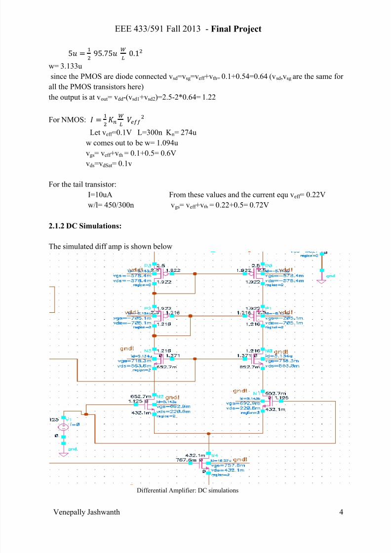
Differential Amplifier
The transistors are marked p0,p1,p2,p3,no,n1,n2,n3,n4 in the schematic.
2.1 DC
2.1.1 Analysis:
The current through the tail transistor is 10uA. Therefore a current of 5uA flows through
each of the two branches of the diff amp.
Let veff =0.1V
The output has to be biased at vdd/2=1.25V.
For PMOS:
8/13/2019 Low-Dropout Voltage Regulator (LDO)
http://slidepdf.com/reader/full/low-dropout-voltage-regulator-ldo 4/30
EEE 433/591 Fall 2013 - Final Project
Venepally Jashwanth 4
w= 3.133u
since the PMOS are diode connected vsd=vsg=veff +vth= 0.1+0.54=0.64 (vsd,vsg are the same for
all the PMOS transistors here)
the output is at vout= vdd-(vsd1+vsd2)=2.5-2*0.64= 1.22
For NMOS:
Let veff =0.1V L=300n K n= 274u
w comes out to be w= 1.094u
vgs= veff +vth = 0.1+0.5= 0.6V
vds=vdSat= 0.1v
For the tail transistor:
I=10uA From these values and the current equ veff = 0.22Vw/l= 450/300n vgs= veff +vth = 0.22+0.5= 0.72V
2.1.2 DC Simulations:
The simulated diff amp is shown below
Differential Amplifier: DC simulations

8/13/2019 Low-Dropout Voltage Regulator (LDO)
http://slidepdf.com/reader/full/low-dropout-voltage-regulator-ldo 5/30
EEE 433/591 Fall 2013 - Final Project
Venepally Jashwanth 5
VGS (mv) IDS (uA) VDS (mv) W(uM)/L(nM)
P0 -705.1 -5.143 -705.1 3.133/300=10.443
P1 -705.1 -5.143 -705.1 3.133/300 =10.443
P2 -578.4 -5.143 -578.4 3.133/300 =10.443
P3 -578.4 -5.143 -578.4 3.133/300 =10.443
N0 629.9 5.143 220.6 1.094/300 = 3.649
N1 629.9 5.143 220.6 1.094/300= 3.649
N2 718.4 5.143 563.6 1.094/300= 3.649
N3 718.4 5.143 563.6 1.094/300= 3.649
N4 757.8 10.27 432.1 450n/300n=1.5
2.1.3. DC Comparisons:
For NMOS: vgs= veff +vth = 0.1+0.5= 0.6V For Tail transistor: vgs=0.22V
vds=vdSat= 0.1v vgs= veff +vth = 0.22+0.5= 0.72V
For PMOS: since the PMOS are diode connected vsd=vsg=veff +vth= 0.1+0.54=0.64 (vsd,vsg are
the same for all the PMOS transistors here)
VGS (mV)
Analysis/
Simulations
IDS (UA)
Analysis/
Simulations
VDS
Analysis/
Simulations
P0 -640/ -705.1 -5/-5.143 -640/ -705.1
P1 -640/ -705.1 -5/-5.143 -640/ -705.1
P2 -640/ -578.4 -5/-5.143 -640/ -578.4
P3 -640/ -578.4 -5/-5.143 -640/ -578.4
N0 600/629.9 5/5.143 100/220.6
N1 600/629.9 5/5.143 100/220.6
N2 600/718.4 5/5.143 100/563.6
N3 600/718.4 5/5.143 100/563.6
N4 720/757.8 10/10.27 220/432.1
The values are close. The error is possibly due to the current equation is an approximation
and further it neglects the channel-length modulation effect.
2.2 AC2.2.1 Analysis:
Output Impedance:
The output impedance can be approximated to be r out= (gmp1*r ds3*r ds1) * (gmn3*r ds3*r ds1)
From cadence: gmp1=68.22u gdsp1=1.103u gdsp3= 1.176u gmn3= 74.14u gds3=2.293u gds1= 3.40u
Therefore r out= 499.4MOhms.
Input Impedance: The current flowing in to the gate is almost zero.
Therefore r in= infnity
Transconductance: Gm=The transconductance for a cascoded diff amp is given by

8/13/2019 Low-Dropout Voltage Regulator (LDO)
http://slidepdf.com/reader/full/low-dropout-voltage-regulator-ldo 6/30
EEE 433/591 Fall 2013 - Final Project
Venepally Jashwanth 6
Gm= -gmp1. gmn1. (r 0p||gmn1r rds1||
) = -gmn1=74.14u
Gain:
Gain: Gm* R out= 74.14u*499M= 80dB
2.2.2 Simulations:
Gain:
gain: 55dB
Input Impedance:
input impedance= 1/1.55E-11=64G Ohms

8/13/2019 Low-Dropout Voltage Regulator (LDO)
http://slidepdf.com/reader/full/low-dropout-voltage-regulator-ldo 7/30
EEE 433/591 Fall 2013 - Final Project
Venepally Jashwanth 7
Output Impedance:
output impedance= 1/9.22E-8=10.8M Ohms
Transconductance: Gm=
transconductance: 1.37E-6
gm Ro Rin gain
Simulations 1.37E-6 10.8M 64G 55dB

8/13/2019 Low-Dropout Voltage Regulator (LDO)
http://slidepdf.com/reader/full/low-dropout-voltage-regulator-ldo 8/30
EEE 433/591 Fall 2013 - Final Project
Venepally Jashwanth 8
2.2.3 Comparison:
gm Ro Rin gainAnalysis 74.4E-6 500M infinity 80dB
Simulations 1.37E-6 10.8M 64G 55dB
2.3 Frequency Response:
2.3.1 Analysis:
The dominant pole is given by
R out( from as calculated in the AC analysis above)= 500M Ohms
cout= cdbp1+cdsn3+cgdn3+cgdp1+cgdn3(1+1/A)= 0.93f( values taken from cadence)
f= 0.34M Hz
2.3.2 Simulations:
Pole freq is around 1M Hz2.3.3 Comparison:
Diff Amp analysis simulations
3-dB pole 0.3 MHz 1MHz

8/13/2019 Low-Dropout Voltage Regulator (LDO)
http://slidepdf.com/reader/full/low-dropout-voltage-regulator-ldo 9/30
EEE 433/591 Fall 2013 - Final Project
Venepally Jashwanth 9
3. Buffer Stage:
Objective:
The objective is to design a buffer stage. Here I implement it using a PMOS buffer.
The buffer is used to avoid the impedance mismatch that exists between a diff amp and
PMOS pass transistor.The output impedance of a cascoded differential amplifier is very high. Connecting
it directly to a driver PMOS transistor would lead to impedance mismatch. Therefore a
voltage buffer is introduced between the two. The buffer stage has high input impedance and
relatively low output impedance. Thus it takes care of impedance matching.
Buffer stage can be implemented by both PMOS or NMOS buffer. The choice of
PMOS buffer is because it operates at relatively low AC voltages at its gate terminal. Since
we are using a cascode Diff Amp in the previous stage, its output AC swing is severely
restricted because of the cascode implementation. So a PMOS buffer would be more
beneficial here.
Specifications:Voltage gain: 1V/V
Input Impedance: High
Output impedance: Low
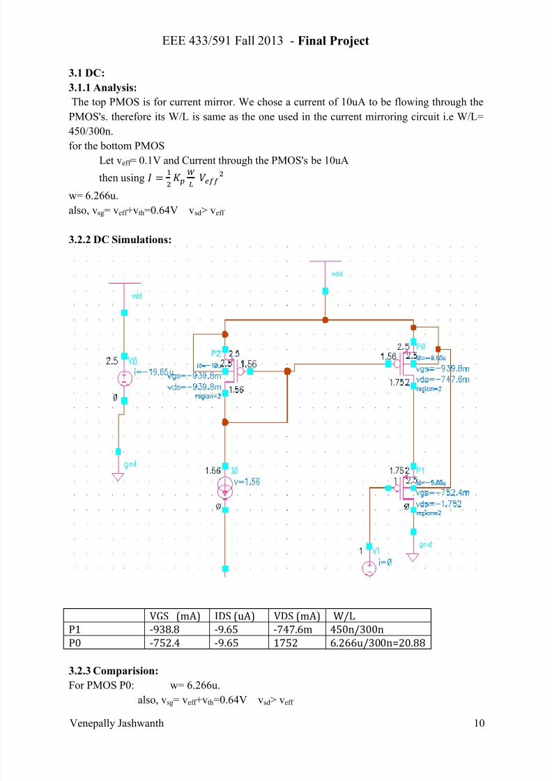
The schematic for buffer is shown below
8/13/2019 Low-Dropout Voltage Regulator (LDO)
http://slidepdf.com/reader/full/low-dropout-voltage-regulator-ldo 10/30
EEE 433/591 Fall 2013 - Final Project
Venepally Jashwanth 10
3.1 DC:
3.1.1 Analysis:
The top PMOS is for current mirror. We chose a current of 10uA to be flowing through the
PMOS's. therefore its W/L is same as the one used in the current mirroring circuit i.e W/L=
450/300n.for the bottom PMOS
Let veff = 0.1V and Current through the PMOS's be 10uA
then using
w= 6.266u.
also, vsg= veff +vth=0.64V vsd> veff
3.2.2 DC Simulations:
VGS (mA) IDS (uA) VDS (mA) W/L
P1 -938.8 -9.65 -747.6m 450n/300n
P0 -752.4 -9.65 1752 6.266u/300n=20.88
3.2.3 Comparision:
For PMOS P0: w= 6.266u.also, vsg= veff +vth=0.64V vsd> veff

8/13/2019 Low-Dropout Voltage Regulator (LDO)
http://slidepdf.com/reader/full/low-dropout-voltage-regulator-ldo 11/30
EEE 433/591 Fall 2013 - Final Project
Venepally Jashwanth 11
P0 VGS (mA) IDS (uA) VDS (mA) W/L
Simulation -752.4 -9.65 1752 6.266u/300n=20.88
Analysis -640m -10u - 6.266u/300n=20.88
3.2 AC
3.2.1 Analysis:
Input Impedance: The current flowing in to the gate is 0
therefore r in= infinity
Output Impedance: r ds0||r ds1
from cadence gds1= 1.853u gds2=1.902u
r out= 0.265MTransconductance: Gm
The transconductance is equal to transconductnce of P0= gm
from Cadence gm=134.5u
AC Voltage Gain:
The AC voltage gain of an amplifier is 1V/V. that is 0dB
3.2.2 AC SIMULATIONS:
Input Impedance:
Input Impedance: 36G

8/13/2019 Low-Dropout Voltage Regulator (LDO)
http://slidepdf.com/reader/full/low-dropout-voltage-regulator-ldo 12/30
EEE 433/591 Fall 2013 - Final Project
Venepally Jashwanth 12
Output Impedance:
output Impedance: 0.84M
Transconductance: gm
gm= 916u

8/13/2019 Low-Dropout Voltage Regulator (LDO)
http://slidepdf.com/reader/full/low-dropout-voltage-regulator-ldo 13/30
EEE 433/591 Fall 2013 - Final Project
Venepally Jashwanth 13
AC gain:
gain=-2.3dB
Parameter gm Ro Rin Gain dBValues 916u 0.84M 36G -2.3
3.2.3 Comparison:
gm Ro Rin Gain dB
Analysis 134.5u 0.26M infinity 0
Simulations 916u 0.84M 36G -2.3
3.3 Frequency Response:
3.3.1 Analysis:
Pole of the buffer as calculated in part 2 of this lab was
taking values from cadence this values turns out to be f p= 41.9M Hz
3.3.2 simulations:
frequency response of buffer: 3-dB pole 515MHz

8/13/2019 Low-Dropout Voltage Regulator (LDO)
http://slidepdf.com/reader/full/low-dropout-voltage-regulator-ldo 14/30
EEE 433/591 Fall 2013 - Final Project
Venepally Jashwanth 14
3.3.3 Comparisons:
Buffer analysis simulations
3-dB pole 41.9M Hz 515MHz
4. Driver Circuit:
Objective:The objective is to design a driver transistor which drives the load. It should be able to
drive a range of currents like 1mA-50mA. Also, the voltage drop across its source-drain
should be less i.e 250mv since we are implementing a low drop-out voltage regulator.
The choice for driver circuit is PMOS source follower. The PMOS source follower is
chosen over NMOS source follower because of the Diff Amp type we have chosen to
implement. The cascode Diff Amp with 9 transistor implementation does not have a large
voltage swing /headroom at its output. This small AC voltage cannot drive a NMOS gate toON state. Whereas for a PMOS no such problem exists because it takes the difference of
Source and Drain voltages.
Requirements:
Current drive: 1mA-50mA
Voltage drop: 250mV
Regulated Voltage: 2.25V
4.1 DC
4.1.1 Analysis:
The output regulated voltage is 2.25V i.e Vdrain=Vd=2.25
Vsource= Vs=2.5V
Vds= 0.25=250m
Vsd> Vsg- |Vtp| ==> Vg > Vd- |Vtp| ==> Vg > 1.71V
Vsg=Vs-Vg< 2.5-1.71= 1.79V
; L=300nM, K p= 95.75u
for I=1mA
upon calculation w turns out to be w= 0.1m
for I=25mA
upon calculation w turns out to be w= 2.5m
for I=25mA
upon calculation w turns out to be w= 5m
For all the cases Vsg and Vsd are shown above

8/13/2019 Low-Dropout Voltage Regulator (LDO)
http://slidepdf.com/reader/full/low-dropout-voltage-regulator-ldo 15/30
EEE 433/591 Fall 2013 - Final Project
Venepally Jashwanth 15
4.2.2 Simulations:
The figures show the DC biasing points of the pass transistor for i=1m,50m,25mA.
The values are tabulated as below.
PASS VGS mV IDS mA VDS mV W/L
For i=1mA -474.9 -1 -249.5 0.1m/300n
For i=25mA -701.6 -25 -250.3 2.5m/300n
For i=50mA -792 -50 -250.6 5m/300n
4.1.3 Comparisons:
VGS Analysis/Simulations IDSAnalysis/
Simulations
VDS (mA)Analysis/
Simulations
For i=1mA <-1.79V/-474.9 -1/-1 -250/-249.5
For i=25mA <-1.79V/-701.6 -25/-25 -250/-250.3
For i=50mA <-1.79V/-792 -50/-50 -250/-250.6
4.2 AC
4.2.1 Analysis:
Input impedance: The current flowing in to the gate is 0.
Therefore r in= infinityOutput impedance: without any load. just for the Pass transistor output impedance = r ds1=
1/gds= 1/41.43m= 24.1 Ohms
Transconductance: The transconcutance is gm= 311.9m A/V
Gain: The gain is gm. r ds = 7.4V/V= 17.5dB

8/13/2019 Low-Dropout Voltage Regulator (LDO)
http://slidepdf.com/reader/full/low-dropout-voltage-regulator-ldo 16/30
EEE 433/591 Fall 2013 - Final Project
Venepally Jashwanth 16
4.2.2 Simulations:
Input impedance:
Input impedance: 1.1M
Output impedance:
Output impedance:158 Ohms

8/13/2019 Low-Dropout Voltage Regulator (LDO)
http://slidepdf.com/reader/full/low-dropout-voltage-regulator-ldo 17/30
EEE 433/591 Fall 2013 - Final Project
Venepally Jashwanth 17
AC gain:
AC gain at low frequency: 34.9dB
Transconductane:
Transconductane= 176m
gm ro gain dB rin
Pass 311.9u 158 Ohms 34.9 1.1M Ohms

8/13/2019 Low-Dropout Voltage Regulator (LDO)
http://slidepdf.com/reader/full/low-dropout-voltage-regulator-ldo 18/30
EEE 433/591 Fall 2013 - Final Project
Venepally Jashwanth 18
4.2.3 Comparisons:
gm Ro Rin Gain dB
Analysis 311.9u 24.1 Ohms infinity 17
Simulations 176m 158 Ohms 1.1M Ohms 34.9
4,3 Frequency response:
4.3.1 Analysis:
The significant pole at the output can be approximated as( as explained in part-2 of the lab
report) :
Taking values from cadence R o= 1/gds=24 Ohms: Cload= 1uF
Therefore f p turns out to be 6.6KHz
4.3.2 Simulations:
Frequency response of pass transistor: pole occurs at 34.5kHz
4.3.3 Comparison:
Pass Transistor analysis simulation
3-dB pole 6.6kHz 34.5kHz

8/13/2019 Low-Dropout Voltage Regulator (LDO)
http://slidepdf.com/reader/full/low-dropout-voltage-regulator-ldo 19/30
EEE 433/591 Fall 2013 - Final Project
Venepally Jashwanth 19
5. Complete System Analysis:
5.1 DC:
For 1mA:
For 25mA:

8/13/2019 Low-Dropout Voltage Regulator (LDO)
http://slidepdf.com/reader/full/low-dropout-voltage-regulator-ldo 20/30
EEE 433/591 Fall 2013 - Final Project
Venepally Jashwanth 20
For 50mA:
For i=1mA
P2 P3 P0 P1 N2 N3 N0 N1 Ntail Pbuff Pdriver
Vgs(mv) -610.8 -610.8 -742 -742.7 720 718.8 692.9 692.8 757 -720 -581.3
Vds(mv) -610.8 -610.8 -742 -691.9 496.2 545.7 218 220.1 432 -1.919 -2.499
Id(uA) -5.135 -5.135 -5.13 -5.135 5.135 5.135 5.135 5.135 10.2 -1.924 -1mA
For i=25mA
P2 P3 P0 P1 N2 N3 N0 N1 Ntail Pbuff Pdriver
Vgs(mv) -610.8 -610.8 -742 -740.8 720 722.2 692.9 693 757 -745.7 -693.1
Vds(mv) -610.8 -610.8 -742 -826.8 496.2 412 219 216.8 432 -1.807 -250
Id(uA) -5.135 -5.135 -5.13 -5.135 5.135 5.135 5.135 5.135 10.2 -1.974 -25mA
For i=50mA
P2 P3 P0 P1 N2 N3 N0 N1 Ntail Pbuff PdriverVgs(mv) -610.8 -610.8 -741 -739.4 720 723.1 692.8 693.1 757 -764.5 -779.5
Vds(mv) -610.8 -610.8 -742 -930.9 496.2 310 219.1 214.1 431 -1.72 -250
Id(uA) -5.132 -5.132 -5.13 -5.132 5.132 5.132 5.132 5.132 10.2 -2.011 -50mA
For all the currents the voltage at the output is regulated at 2.25V. The figures for DC
are shown above the tables.

8/13/2019 Low-Dropout Voltage Regulator (LDO)
http://slidepdf.com/reader/full/low-dropout-voltage-regulator-ldo 21/30
EEE 433/591 Fall 2013 - Final Project
Venepally Jashwanth 21
5.2 AC:
Magnitude and phase plots of the overall system:
for i=1mA
Gain= 91.76dB
Gain crossover: wgx= 2.087MHz
Phase Crossover: w px =1.119MHz
wgx> w px==> Overall system is unstable
Poles: one pole at95.5Hz, 108.7kHz, 1MHz
Zeros: Zero at 949.9Hz

8/13/2019 Low-Dropout Voltage Regulator (LDO)
http://slidepdf.com/reader/full/low-dropout-voltage-regulator-ldo 22/30
EEE 433/591 Fall 2013 - Final Project
Venepally Jashwanth 22
for i=25mA
Gain= 82.55dB
Gain crossover: wgx= 4.659MHz
Phase Crossover: w px =1.018MHz
wgx> w px==> Overall system is unstable
Poles: one pole at 8.598KHz, 637.5kHz,2MHz
Zeros: Zero at 91.56kHz
Phase margin: -248+180=-68
for i=50mA
Gain= 71.61dB

8/13/2019 Low-Dropout Voltage Regulator (LDO)
http://slidepdf.com/reader/full/low-dropout-voltage-regulator-ldo 23/30

8/13/2019 Low-Dropout Voltage Regulator (LDO)
http://slidepdf.com/reader/full/low-dropout-voltage-regulator-ldo 24/30
EEE 433/591 Fall 2013 - Final Project
Venepally Jashwanth 24
Frequency response of buffer for 25mA
Diff Amp Buffer
gain dB 56.87 55.1
3dB pole 484.4k 589.4k
gain crossover 294.9M 23.7M
phase crossover - -
Overall open loop System gain is without compensation: 71.6dBBandwidth: 5.16M Hz
5.3 Transient uncompensated:
vripple= (2.37-2.1)/2.5= 0.108%
Settling time: the system was found to be unstable. In fact it was found to be marginally
stable. So it keeps oscillating.

8/13/2019 Low-Dropout Voltage Regulator (LDO)
http://slidepdf.com/reader/full/low-dropout-voltage-regulator-ldo 25/30
EEE 433/591 Fall 2013 - Final Project
Venepally Jashwanth 25
5.5 Compensated system:
The system above was found to be unstable. Therefore I compensated it with a capacitor. A
capacitor at the output adds an extra pole. Therefore the gain falls faster than in the previous
case. By the time it reaches w px, it would have fallen adequately so that at phase crossover its
gain is less than 1. hence the system stabilizes. The capacitance value that i chose tocompensate is 50uF
5.5.1 AC
The magnitude and phase plots of the overall system:
for 1mA:
for 25mA:

8/13/2019 Low-Dropout Voltage Regulator (LDO)
http://slidepdf.com/reader/full/low-dropout-voltage-regulator-ldo 26/30
EEE 433/591 Fall 2013 - Final Project
Venepally Jashwanth 26
for 50mA:
for 1mA for 25mA for 50mA
gain dB 83.3 82.34 71.6
gain crossover Hz 18.6k 203.6K 243K
phase crossover Hz 1.17M 996.9K 1.057m
phase margin deg 89 68.8 67
poles Hz 1.98,1.047M,10M 1100.4,55.88K,9.7M 102, 243.9K,1.69Mzeros Hz 28.08 304K 1.479K
The magnitude and phase plots for the individual blocks:
at the differential amplifier:

8/13/2019 Low-Dropout Voltage Regulator (LDO)
http://slidepdf.com/reader/full/low-dropout-voltage-regulator-ldo 27/30
EEE 433/591 Fall 2013 - Final Project
Venepally Jashwanth 27
at buffer:
Diff Amp Buffer
gain dB 55.8 54
3dB pole 456.8k 56.1k
gain crossover 294.6M 23.7M
phase crossover - -
5.5.2 Transient response:
the transient response after compensation is given by
Upon zooming in, the same graph looks like
8/13/2019 Low-Dropout Voltage Regulator (LDO)
http://slidepdf.com/reader/full/low-dropout-voltage-regulator-ldo 28/30
EEE 433/591 Fall 2013 - Final Project
Venepally Jashwanth 28
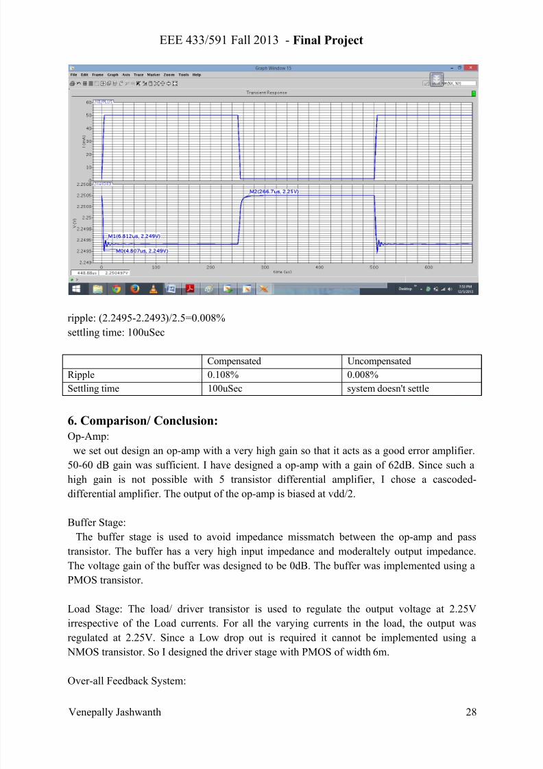
ripple: (2.2495-2.2493)/2.5=0.008%
settling time: 100uSec
Compensated Uncompensated
Ripple 0.108% 0.008%
Settling time 100uSec system doesn't settle
6. Comparison/ Conclusion:
Op-Amp:
we set out design an op-amp with a very high gain so that it acts as a good error amplifier.
50-60 dB gain was sufficient. I have designed a op-amp with a gain of 62dB. Since such a
high gain is not possible with 5 transistor differential amplifier, I chose a cascoded-
differential amplifier. The output of the op-amp is biased at vdd/2.
Buffer Stage:
The buffer stage is used to avoid impedance missmatch between the op-amp and passtransistor. The buffer has a very high input impedance and moderaltely output impedance.
The voltage gain of the buffer was designed to be 0dB. The buffer was implemented using a
PMOS transistor.
Load Stage: The load/ driver transistor is used to regulate the output voltage at 2.25V
irrespective of the Load currents. For all the varying currents in the load, the output was
regulated at 2.25V. Since a Low drop out is required it cannot be implemented using a
NMOS transistor. So I designed the driver stage with PMOS of width 6m.
Over-all Feedback System:

8/13/2019 Low-Dropout Voltage Regulator (LDO)
http://slidepdf.com/reader/full/low-dropout-voltage-regulator-ldo 29/30
EEE 433/591 Fall 2013 - Final Project
Venepally Jashwanth 29
The feedback is used to sample a part of the output voltage to the op-amp so that it can do
corrections necessary so as to maintain the voltage at 2.25V. The feedback circuitry was
implemented using resistor voltage divider circuit. Since we chose to implement it using
resistors, not much variations occur in their values. Hence although variations occur in the
active devices, the passive resistors are not prone to changes. hence the output gain can bemaintained constant.
6.1 DC Parameters:
For the various currents, all the transistors have to be maintained in saturation under all
conditions. also, the output has to be regulated at 2.25V.
The DC operating points of the transistors at various currents in the feedback is shown in the
tables below.
For i=1mA
P2 P3 P0 P1 N2 N3 N0 N1 Ntail Pbuff Pdriver
Vgs(mv) -610.8 -610.8 -742 -742.7 720 718.8 692.9 692.8 757 -720 -581.3
Vds(mv) -610.8 -610.8 -742 -691.9 496.2 545.7 218 220.1 432 -1.919 -2.499
Id(uA) -5.135 -5.135 -5.13 -5.135 5.135 5.135 5.135 5.135 10.2 -1.924 -1mA
For i=25mA
P2 P3 P0 P1 N2 N3 N0 N1 Ntail Pbuff Pdriver
Vgs(mv) -610.8 -610.8 -742 -740.8 720 722.2 692.9 693 757 -745.7 -693.1
Vds(mv) -610.8 -610.8 -742 -826.8 496.2 412 219 216.8 432 -1.807 -250
Id(uA) -5.135 -5.135 -5.13 -5.135 5.135 5.135 5.135 5.135 10.2 -1.974 -25mA
For i=50mA
P2 P3 P0 P1 N2 N3 N0 N1 Ntail Pbuff Pdriver
Vgs(mv) -610.8 -610.8 -741 -739.4 720 723.1 692.8 693.1 757 -764.5 -779.5
Vds(mv) -610.8 -610.8 -742 -930.9 496.2 310 219.1 214.1 431 -1.72 -250
Id(uA) -5.132 -5.132 -5.13 -5.132 5.132 5.132 5.132 5.132 10.2 -2.011 -50mA
6.2 AC Parameters:
The various AC parameters are summarized in the tables below:
Differential Amp Buffer Pass
Gain (dB) f3dB (MHz) P2 P3 Unity BW
Analysis 80 0.3M 41.9M 6.6K -
Simulation 55 1M 515M 34.5K 5.16M
Error % 31 70 91 80
Final Discussion:
An LDO is designed with a regulated voltage of 2.25V. The transient analysis is plotted and
the ripple time is found to be 0.18%. Settling time is 100usec.

8/13/2019 Low-Dropout Voltage Regulator (LDO)
http://slidepdf.com/reader/full/low-dropout-voltage-regulator-ldo 30/30
EEE 433/591 Fall 2013 - Final Project
Output Regulated Voltage: 2.25V
Ripple: 0.18%
Settling time: 100usec
Issues: Initially an LDO was designed but it was found to be unstable. We Did not haveenough phase margin. Then I used compensation techniques to adjust the poles so that the
overall feedback system was stable. I did the compensation using a capacitor of 60uF at the
load. The uncompensated and compensated phase margins was found to be
For uncompensated:
for 1mA for 25mA for 50mA
gain dB 91.76 82.5 71.6
gain crossover Hz 2.087M 4.659M 5.156M
phase crossover Hz 1.119MM 1.028M 1.105M
phase margin deg - - -
For compensated:
for 1mA for 25mA for 50mA
gain dB 83.3 82.34 71.6
gain crossover Hz 18.6k 203.6K 243K
phase crossover Hz 1.17M 996.9K 1.057m
phase margin deg 89 68.8 67
Improvements:
Since the compensation was done using a capacitor at the output, slew rate at the output
decreases. Instead by using lead compensation technique this can be avoided.
To make the system insusceptible to changes in the output load, a high gain error amplifier
may be used.
The settling time was found to be 100usec. In application where this amount of settling time
is not acceptable, I can decrease it by using higher current drive in the LDO and by chooisng
a Q-factor that is optimal.
Result: I have designed an LDO with the required specifications.