Light extraction efficiency enhancement of InGaN...
11
Light extraction efficiency enhancement of InGaN quantum wells light-emitting diodes with polydimethylsiloxane concave microstructures Yik-Khoon Ee, 1,* Pisist Kumnorkaew, 2 Ronald A. Arif, 1 Hua Tong, 1 James F. Gilchrist, 2 and Nelson Tansu 1,+ 1 Center for Optical Technologies, Department of Electrical and Computer Engineering, Lehigh University, Bethlehem, PA 18015, USA 2 Center for Advanced Materials and Nanotechnology, Department of Chemical Engineering, Lehigh University, Bethlehem, PA 18015, USA *[email protected], + [email protected] Abstract: Improvement of light extraction efficiency of InGaN light emitting diodes (LEDs) using polydimethylsiloxane (PDMS) concave microstructures arrays was demonstrated. The size effect of the concave microstructures on the light extraction efficiency of III-Nitride LEDs was studied. Depending on the size of the concave microstructures, ray tracing simulations show that the use of PDMS concave microstructures arrays can lead to increase in light extraction efficiency of InGaN LEDs by 1.5 to 2.0 times. Experiments utilizing 2.0 micron thick PDMS with 1.0 micron diameter of the PDMS concave microstructures arrays demonstrated 1.70 times improvement in light extraction efficiency, which is consistent with improvement of 1.77 times predicted from simulation. The enhancement in light extraction efficiency is attributed to increase in effective photon escape cone due to PDMS concave microstructures arrays. ©2009 Optical Society of America OCIS codes: (230.3670) Light-Emitting Diodes; (230.0250) Optoelectronics. References and links 1. Need Project, Intermediate Energy Infobook, (US Department of Energy, pp. 51, 2008). 2. E. F. Schubert, Light Emitting Diodes, (Cambridge University Press, pp. 145, 2006). 3. S. Nakamura, and S. Pearton, S., and G. Fasol, The Blue Laser Diode, (Springer-Verlag Berlin Heidelberg, pp. 7, 2000). 4. R. A. Arif, Y. K. Ee, and N. Tansu, “Polarization Engineering via Staggered InGaN Quantum Wells for Radiative Efficiency Enhancement of Light Emitting Diodes,” Appl. Phys. Lett. 91(9), 091110 (2007). 5. R. A. Arif, H. Zhao, Y. K. Ee, and N. Tansu, “Spontaneous Emission and Characteristics of Staggered InGaN Quantum Wells Light Emitting Diodes,” IEEE J. Quantum Electron. 44(6), 573–580 (2008). 6. H. Zhao, R. A. Arif, and N. Tansu, “Design Analysis of Staggered InGaN Quantum Wells Light-Emitting Diodes at 500-540 nm,” IEEE J. Sel. Top. Quantum Electron. 15, 1104–1114 (2009). 7. H. Zhao, R. A. Arif, and N. Tansu, “Self Consistent Gain Analysis of Type-II ‘W’ InGaN-GaNAs Quantum Well Lasers,” J. Appl. Phys. 104(4), 043104 (2008). 8. H. Zhao, R. A. Arif, Y. K. Ee, and N. Tansu, “Self-Consistent Analysis of Strain-Compensated InGaN-AlGaN Quantum Wells for Lasers and Light Emitting Diodes,” IEEE J. Quantum Electron. 45(1), 66–78 (2009). 9. C. Huh, K. S. Lee, E. J. Kang, and S. J. Park, “Improved light-output and electrical performance of InGaN-based light-emitting diode by microroughening of the p-GaN surface,” J. Appl. Phys. 93(11), 9383–9385 (2003). 10. T. Fujii, Y. Gao, R. Sharma, E. L. Hu, S. P. DenBaars, and S. Nakamura, “Increase in the extraction efficiency of GaN-based light-emitting diodes via surface roughening,” Appl. Phys. Lett. 84(6), 855–857 (2004). 11. C. F. Lin, Z. J. Yang, J. H. Zheng, and J. J. Dai, “Enhanced light output in nitride-based light-emitting diodes by roughening the mesa sidewall,” IEEE Photon. Technol. Lett. 17(10), 2038–2040 (2005). 12. S. J. Lee, J. Lee, S. Kim, and H. Jeon, “Fabrication of reflective GaN mesa sidewalls for the application to high extraction efficiency LEDs,” Phys. Stat. Solidi (c) 4, 2625- 2628 (2007). 13. T. Kim, A. J. Danner, and K. D. Choquette, “Enhancement in external quantum efficiency of blue light-emitting diode by photonic crystal surface grating,” Electron. Lett. 41(20), 1138–1139 (2005). 14. J. J. Wierer, M. R. Krames, J. E. Epler, N. F. Gardner, J. R. Wendt, M. M. Sigalas, S. R. J. Brueck, D. Li, and M. Shagam, “III-nitride LEDs with photonic crystal structures”, in Proc. SPIE, 5739, 102–107 (2005). #109161 - $15.00 USD Received 1 Apr 2009; revised 20 Jul 2009; accepted 21 Jul 2009; published 24 Jul 2009 (C) 2009 OSA 3 August 2009 / Vol. 17, No. 16 / OPTICS EXPRESS 13747
Transcript of Light extraction efficiency enhancement of InGaN...

Light extraction efficiency enhancement of InGaN quantum wells light-emitting diodes with polydimethylsiloxane concave microstructures
Yik-Khoon Ee,1,*
Pisist Kumnorkaew,2 Ronald A. Arif,
1 Hua Tong,
1 James F. Gilchrist,
2
and Nelson Tansu1,+
1Center for Optical Technologies, Department of Electrical and Computer Engineering, Lehigh University,
Bethlehem, PA 18015, USA 2Center for Advanced Materials and Nanotechnology, Department of Chemical Engineering, Lehigh University,
Bethlehem, PA 18015, USA *[email protected], [email protected]
Abstract: Improvement of light extraction efficiency of InGaN light emitting diodes (LEDs) using polydimethylsiloxane (PDMS) concave microstructures arrays was demonstrated. The size effect of the concave microstructures on the light extraction efficiency of III-Nitride LEDs was studied. Depending on the size of the concave microstructures, ray tracing simulations show that the use of PDMS concave microstructures arrays can lead to increase in light extraction efficiency of InGaN LEDs by 1.5 to 2.0 times. Experiments utilizing 2.0 micro n thick PDMS with 1.0 micron diameter of the PDMS concave microstructures arrays demonstrated 1.70 times improvement in light extraction efficiency, which is consistent with improvement of 1.77 times predicted from simulation. The enhancement in light extraction efficiency is attributed to increase in effective photon escape cone due to PDMS concave microstructures arrays.
©2009 Optical Society of America
OCIS codes: (230.3670) Light-Emitting Diodes; (230.0250) Optoelectronics.
References and links
1. Need Project, Intermediate Energy Infobook, (US Department of Energy, pp. 51, 2008). 2. E. F. Schubert, Light Emitting Diodes, (Cambridge University Press, pp. 145, 2006). 3. S. Nakamura, and S. Pearton, S., and G. Fasol, The Blue Laser Diode, (Springer-Verlag Berlin Heidelberg, pp. 7,
2000). 4. R. A. Arif, Y. K. Ee, and N. Tansu, “Polarization Engineering via Staggered InGaN Quantum Wells for
Radiative Efficiency Enhancement of Light Emitting Diodes,” Appl. Phys. Lett. 91(9), 091110 (2007). 5. R. A. Arif, H. Zhao, Y. K. Ee, and N. Tansu, “Spontaneous Emission and Characteristics of Staggered InGaN
Quantum Wells Light Emitting Diodes,” IEEE J. Quantum Electron. 44(6), 573–580 (2008). 6. H. Zhao, R. A. Arif, and N. Tansu, “Design Analysis of Staggered InGaN Quantum Wells Light-Emitting Diodes
at 500-540 nm,” IEEE J. Sel. Top. Quantum Electron. 15, 1104–1114 (2009). 7. H. Zhao, R. A. Arif, and N. Tansu, “Self Consistent Gain Analysis of Type-II ‘W’ InGaN-GaNAs Quantum Well
Lasers,” J. Appl. Phys. 104(4), 043104 (2008). 8. H. Zhao, R. A. Arif, Y. K. Ee, and N. Tansu, “Self-Consistent Analysis of Strain-Compensated InGaN-AlGaN
Quantum Wells for Lasers and Light Emitting Diodes,” IEEE J. Quantum Electron. 45(1), 66–78 (2009). 9. C. Huh, K. S. Lee, E. J. Kang, and S. J. Park, “Improved light-output and electrical performance of InGaN-based
light-emitting diode by microroughening of the p-GaN surface,” J. Appl. Phys. 93(11), 9383–9385 (2003). 10. T. Fujii, Y. Gao, R. Sharma, E. L. Hu, S. P. DenBaars, and S. Nakamura, “Increase in the extraction efficiency of
GaN-based light-emitting diodes via surface roughening,” Appl. Phys. Lett. 84(6), 855–857 (2004). 11. C. F. Lin, Z. J. Yang, J. H. Zheng, and J. J. Dai, “Enhanced light output in nitride-based light-emitting diodes by
roughening the mesa sidewall,” IEEE Photon. Technol. Lett. 17(10), 2038–2040 (2005). 12. S. J. Lee, J. Lee, S. Kim, and H. Jeon, “Fabrication of reflective GaN mesa sidewalls for the application to high
extraction efficiency LEDs,” Phys. Stat. Solidi (c) 4, 2625- 2628 (2007). 13. T. Kim, A. J. Danner, and K. D. Choquette, “Enhancement in external quantum efficiency of blue light-emitting
diode by photonic crystal surface grating,” Electron. Lett. 41(20), 1138–1139 (2005). 14. J. J. Wierer, M. R. Krames, J. E. Epler, N. F. Gardner, J. R. Wendt, M. M. Sigalas, S. R. J. Brueck, D. Li, and M.
Shagam, “III-nitride LEDs with photonic crystal structures”, in Proc. SPIE, 5739, 102–107 (2005).
#109161 - $15.00 USD Received 1 Apr 2009; revised 20 Jul 2009; accepted 21 Jul 2009; published 24 Jul 2009
(C) 2009 OSA 3 August 2009 / Vol. 17, No. 16 / OPTICS EXPRESS 13747

15. K. McGroddy, A. David, E. Matioli, M. Iza, S. Nakamura, S. DenBaars, J. S. Speck, C. Weisbuch, and E. L. Hu, “Directional emission control and increased light extraction in GaN photonic crystal light emitting diodes,” Appl. Phys. Lett. 93(10), 103502 (2008).
16. H. W. Choi, C. Liu, E. Gu, G. McConnell, J. M. Girkin, I. M. Watson, and M. D. Dawson, “GaN micro-light-emitting diode arrays with monolithically integrated sapphire microlenses,” Appl. Phys. Lett. 84(13), 2253–2255 (2004).
17. J. Q. Xi, H. Luo, A. J. Pasquale, J. K. Kim, and E. F. Schubert, “Enhanced light extraction in GaInN light-emitting diode with pyramid reflector,” IEEE Photon. Technol. Lett. 18(22), 2347–2349 (2006).
18. J. K. Kim, M. F. Schubert, J. Q. Xi, F. W. Mont, and E. F. Schubert, “Enhancement of light extraction in GaInN light-emitting diodes with graded-index indium tin oxide layer”, in Proc. of the Conference on Lasers and Electro-Optics (Baltimore, MD, 2007) Paper No. CTuI1.
19. J. Q. Xi, M. F. Schubert, J. K. Kim, E. F. Schubert, M. Chen, S. Y. Lin, W. Liu, and J. A. Smart, “Optical thin-film materials with low refractive index for broadband elimination of Fresnel reflection,” Nat. Photonics 1, 176–179 (2007).
20. A. J. Fischer, F. W. Mont, J. K. Kim, E. F. Schubert, D. D. Koleske, and M. H. Crawford, “Enhanced Light-Extraction from InGaN Quantum Wells Using Refractive-Index-Matched TiO2”, in Proc. of the Conference on Lasers and Electro-Optics (Baltimore, MD, 2007) Paper No. CTuI2.
21. Y. K. Ee, P. Kumnorkaew, R. A. Arif, J. F. Gilchrist, and N. Tansu, “Enhancement of light extraction efficiency of InGaN quantum wells light emitting diodes using SiO2/polystyrene microlens arrays,” Appl. Phys. Lett. 91(22), 221107 (2007).
22. P. Kumnorkaew, Y. K. Ee, N. Tansu, and J. F. Gilchrist, “Investigation of the deposition of microsphere monolayers for fabrication of microlens arrays,” Langmuir 24(21), 12150–12157 (2008).
23. Y. K. Ee, P. Kumnorkaew, R. A. Arif, H. Tong, H. Zhao, J. F. Gilchrist, and N. Tansu, “Optimization of Light Extraction Efficiency of III-Nitride Light Emitting Diodes with Self-Assembled Colloidal-based Microlenses,” IEEE J. Sel. Top. Quantum Electron. 15, 1218–1225 (2009).
24. E. H. Park, J. Jang, S. Gupta, I. Ferguson, C. H. Kim, S. K. Jeon, and J. S. Park, “Air-voids embedded high efficiency InGaN-light emitting diode,” Appl. Phys. Lett. 93(19), 191103 (2008).
25. R. Horvath, L. R. Lindvold, and N. B. Larsen, “Fabrication of all-polymer freestanding waveguides,” J. Micromech. Microeng. 13(3), 419–424 (2003).
26. B. G. Prevo, and O. D. Velev, “Controlled, rapid deposition of structured coatings from micro- and nanoparticle suspensions,” Langmuir 20(6), 2099–2107 (2004).
27. J. E. Mark, Handbook of Polymers, (Oxford University Press, pp. 424, 1999). 28. J. Zou, D. Kotchetkov, A. A. Balandin, D. I. Florescu, and F. H. Pollak, “Thermal conductivity of GaN films:
Effects of impurities and dislocations,” J. Appl. Phys. 92(5), 2534–2539 (2002). 29. N. Tansu, and L. J. Mawst, “Current Injection Efficiency of 1300-nm InGaAsN Quantum-Well Lasers,” J. Appl.
Phys. 97(5), 054502 (2005).
1. Introduction
The rising energy cost has pushed for technological advances for high energy-efficiency technology. The United States spends more than $37 billion annually on energy for lighting alone [1]. One of the long term strategies adopted to reduce the energy consumption is solid state lighting through the use of light emitting diodes (LEDs). The LED technology represents a disruptive technology that has the potential to displace its less energy efficient lighting devices such as incandescent and fluorescent lamps. High efficiency InGaN quantum wells (QW) LEDs [2–4] in particular have already been used in applications such as full color displays, traffic signals, backlighting for liquid crystal displays as well as solid state lighting.
The external quantum efficiency ( EQEη ) of LEDs can be expressed as the product of
current injection efficiency ( injη ), radiative efficiency ( radη ), and light extraction efficiency
( extractionη ). The light extraction efficiency is defined as the fraction of photons generated in
the active region of semiconductor that escapes into free space. In addition to challenges in achieving high radiative efficiency and current injection efficiency in InGaN QW LEDs [4–8], light extraction efficiency optimization in nitride-based LEDs is important for achieving high-efficiency devices. Unfortunately, the refractive index difference of GaN (n = 2.5) is relatively large compared to air (n = 1). The large refractive indices mismatch results in a narrow escape cone of only 23.5° with escape probability of only 4% from the top surface of the LED devices, with the rest of the optical power trapped within the semiconductor.
To overcome the light extraction limitation in nitride LED, several novel approaches have been pursued [9–20]. One approach is to roughen the top surface of the LEDs, which will lead to enhanced scattering of light generated from the active region at the roughened GaN / air
#109161 - $15.00 USD Received 1 Apr 2009; revised 20 Jul 2009; accepted 21 Jul 2009; published 24 Jul 2009
(C) 2009 OSA 3 August 2009 / Vol. 17, No. 16 / OPTICS EXPRESS 13748

interface. The surface roughening technique could be accomplished by using wet etching [9] or photochemical etching [10], however the roughness obtained using these methods were not uniform thus leading to variation in the light extraction efficiency improvement of the LEDs across the wafer sample. Besides roughening the top surface emission area of the LEDs, other research groups have tried to roughen the mesa sidewalls of the LEDs using photochemical etching [11]. Similarly, the surface of the mesa sidewalls was non-uniform. Another approach to increase the light extraction efficiency of the LEDs was to use an oblique mesa sidewall [12], which can be achieved by using reflowed photoresist and adjusting the flow of CF4 gas during the dry etch process. The improvement of the light extraction efficiency in LED employing oblique mesa sidewall [12] was isolated to the areas in the sidewall regions only. Photonic crystal structures can also be utilized to enhance the light extraction efficiency of LEDs [13–15], but this approach requires the use of electron beam or complex laser holographic lithography due to the small dimensions of the photonic crystal structures. Other approaches to improve light extraction efficiency in III-Nitride LEDs also include sapphire microlens approach [16], nanopyramid approach [17], and grading refractive indices between GaN / air interface with planar materials approach [18–20]. Recently, we demonstrated a novel approach to significantly enhance the light extraction efficiency of III-Nitride LEDs by fabricating SiO2 / polystyrene (PS) microlens arrays [21–23].
Here, we present a novel technique to increase the light extraction efficiency of III-Nitride LEDs using polydimethylsiloxane (PDMS) concave microstructures arrays. In our previous work on SiO2 / PS microlens arrays [21–23], we formed convex lens-like microstructures on top emission area of the LEDs by semi-burying SiO2 microspheres in planar polystyrene by using rapid convective deposition method. In this work, specifically we employed SiO2 microsphere arrays as a template to form concave microstructures arrays in the PDMS layer on top of the LEDs (Fig. 1) by using imprinting method. The use of imprinting method leads to a low cost and scalable approach to enhance the light extraction efficiency of the LEDs. The use of concave microstructures arrays, instead of convex microstructures, on top of LEDs also leads to improved self-focusing effect of the extracted photons. The size effect of the PDMS concave microstructures arrays on the light extraction efficiency of InGaN QWs LEDs has been studied. The experimental and simulation results will be compared with those of planar LEDs.
C-plane Sapphire Substrate
n – Contact
25-Å InxGa1-xN / 120-Å u-GaN
n – GaN template
p – Contact PDMS concavemicrostructures arrays
GaN Buffer
p – GaN
4 x
Fig. 1. Schematic of InGaN QWs LEDs structure utilizing PDMS concave microstructures arrays, on the top emitting InGaN LED.
2. Computation of light extraction efficiency via Monte Carlo ray tracing
To study the effect of PDMS concave microstructures arrays on the light extraction of InGaN QWs LED, simulation studies were conducted using Monte Carlo ray tracings. Monte Carlo technique was used to calculate the light extraction efficiency by treating the entire LED device structure as a physical optics problem, and tracking the rays emanating from the quantum wells active region of the device. Note that wave-optics based modeling will provide improved accuracy in the simulation of the structure. However, Monte Carlo ray tracing is sufficient for simulating our current device structure [24], due to the micron-sized features
#109161 - $15.00 USD Received 1 Apr 2009; revised 20 Jul 2009; accepted 21 Jul 2009; published 24 Jul 2009
(C) 2009 OSA 3 August 2009 / Vol. 17, No. 16 / OPTICS EXPRESS 13749

employed in the our devices. The spontaneous emission of the InGaN QWs were computed and used as the light source in the ray tracing simulation. The interaction of the ray traced photons and carrier transport is carried out in three-dimensions self-consistently. Photon recycling recombination process was also taken into account in the simulation. The quantum wells active domain comprises of 74,000 vertices (20 rays in each vertex) with 1.48 million light rays used in the simulations to minimize statistical error to less than 0.1%. The schematic of the simulation mesh structure of the LED device utilizing the PDMS concave microstructures arrays is shown in Fig. 2(a).
Air
PDMS
PDMS Concave Microstructures Arrays
Define LED physical structure, and input material parameters
Define LED device simulation parameters
Compute spontaneous emission from active
regions: 4 period quantum wells
Raytracing of emission from active regions
Terminate rays after preset minimum
intensity has been reached
Light extraction efficiency obtainedfrom outgoing rays
Photon recycling, Photon re-absorption processes included
(a) (b)
Fig. 2. (a) Schematic of InGaN QWs LEDs simulation mesh structure utilizing PDMS concave microstructures arrays on the top emission surface, and (b) flow chart of Monte Carlo ray tracing simulation to calculate the light extraction efficiency of the LED.
The LED structure in the simulation comprises of a 100µm x 100µm mesa size LED device structure grown on 2.5µm n-GaN virtual template on 400µm thick sapphire substrate. The active region consists of 4 periods of 2.5nm InGaN/GaN QWs, capped with 0.1µm p-doped GaN used as the top contact layer. Finally, a layer of PDMS concave microstructures was designed on top of the emission region. The flow chart of the Monte Carlo simulation is shown in Fig. 2(b). First the physical LED structure was defined, together with the input material parameters such as refractive index. The refractive index of PDMS (Sylgard 184) used in the simulation was 1.43 [25]. Additional LED ray tracing parameters such as number of rays per vertex, minimum intensity of ray before raytracing terminates were also defined. Ray tracing of the photons starts with the spontaneous emission from the active region, which comprises of a 4-period InGaN QWs. Tracing of the trapped rays were terminated after a preset minimum intensity has been reached. Light extraction efficiency was then obtained from the analysis of the outgoing rays from the LED structure. To provide useful comparison in our studies, the ratio of the light extraction efficiency of the III-Nitride LED employing PDMS concave microstructure arrays with that of planar LED is compared for various microstructure diameter (dconcave) and PDMS layer thicknesses with various emission wavelengths.
To investigate the size effect of PDMS concave microstructures arrays on the light extraction efficiency of III-nitride LEDs, ray tracing simulation was done for LEDs with light emission area coated with PDMS concave microstructures arrays. Figures 3(a) and 3(b) show the ratios of the light extraction efficiencies of the LEDs with concave microstructures arrays compared to the planar LED, with PDMS layer thicknesses of 3.0µm and 2.0µm, respectively.
#109161 - $15.00 USD Received 1 Apr 2009; revised 20 Jul 2009; accepted 21 Jul 2009; published 24 Jul 2009
(C) 2009 OSA 3 August 2009 / Vol. 17, No. 16 / OPTICS EXPRESS 13750
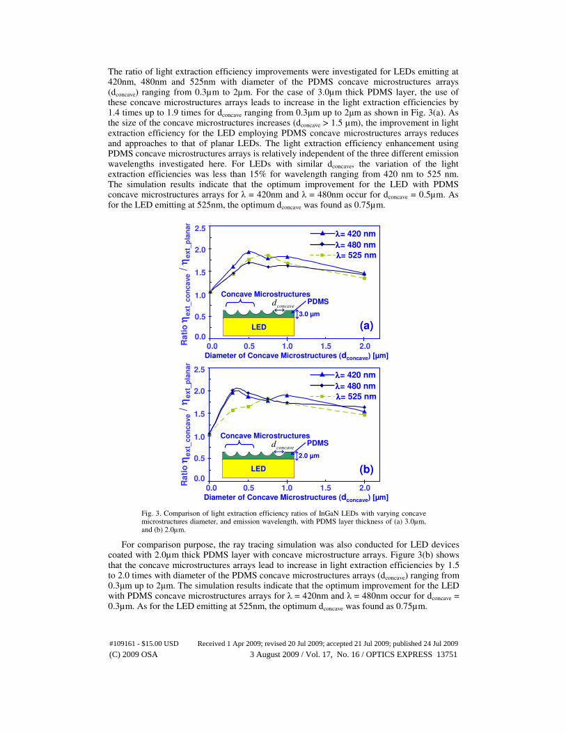
The ratio of light extraction efficiency improvements were investigated for LEDs emitting at 420nm, 480nm and 525nm with diameter of the PDMS concave microstructures arrays (dconcave) ranging from 0.3µm to 2µm. For the case of 3.0µm thick PDMS layer, the use of these concave microstructures arrays leads to increase in the light extraction efficiencies by 1.4 times up to 1.9 times for dconcave ranging from 0.3µm up to 2µm as shown in Fig. 3(a). As the size of the concave microstructures increases (dconcave > 1.5 µm), the improvement in light extraction efficiency for the LED employing PDMS concave microstructures arrays reduces and approaches to that of planar LEDs. The light extraction efficiency enhancement using PDMS concave microstructures arrays is relatively independent of the three different emission wavelengths investigated here. For LEDs with similar dconcave, the variation of the light extraction efficiencies was less than 15% for wavelength ranging from 420 nm to 525 nm. The simulation results indicate that the optimum improvement for the LED with PDMS concave microstructures arrays for λ = 420nm and λ = 480nm occur for dconcave = 0.5µm. As for the LED emitting at 525nm, the optimum dconcave was found as 0.75µm.
0.0
0.5
1.0
1.5
2.0
2.5
0.00 1.00 2.00
LED
Concave MicrostructuresPDMS
λλλλ= 420 nm
ηex
t_m
icro
len
sη
ext_
pla
nar
λλλλ= 480 nmλλλλ= 525 nm
2.5
2.0
1.5
1.0
0.5
0.0
Rat
io ηη ηη
ext_
con
cave
/ ηη ηηex
t_p
lan
ar
0.0 0.5 1.0 1.5 2.0Diameter of Concave Microstructures (dconcave) [µm]
3.0 µmconcaved
0.0
0.5
1.0
1.5
2.0
2.5
0.00 1.00 2.00
LED
Concave MicrostructuresPDMS
λλλλ= 420 nm
ηex
t_m
icro
len
sη
ext_
pla
nar
λλλλ= 480 nmλλλλ= 525 nm
2.5
2.0
1.5
1.0
0.5
0.0
Rat
io ηη ηη
ext_
con
cave
/ ηη ηηex
t_p
lan
ar
0.0 0.5 1.0 1.5 2.0Diameter of Concave Microstructures (dconcave) [µm]
2.0 µmconcaved
(a)
(b)
Fig. 3. Comparison of light extraction efficiency ratios of InGaN LEDs with varying concave microstructures diameter, and emission wavelength, with PDMS layer thickness of (a) 3.0µm, and (b) 2.0µm.
For comparison purpose, the ray tracing simulation was also conducted for LED devices coated with 2.0µm thick PDMS layer with concave microstructure arrays. Figure 3(b) shows that the concave microstructures arrays lead to increase in light extraction efficiencies by 1.5 to 2.0 times with diameter of the PDMS concave microstructures arrays (dconcave) ranging from 0.3µm up to 2µm. The simulation results indicate that the optimum improvement for the LED with PDMS concave microstructures arrays for λ = 420nm and λ = 480nm occur for dconcave = 0.3µm. As for the LED emitting at 525nm, the optimum dconcave was found as 0.75µm.
#109161 - $15.00 USD Received 1 Apr 2009; revised 20 Jul 2009; accepted 21 Jul 2009; published 24 Jul 2009
(C) 2009 OSA 3 August 2009 / Vol. 17, No. 16 / OPTICS EXPRESS 13751

3. Experimental works and discussions
A monolayer of SiO2 microsphere arrays was first deposited on a glass slide using the low-cost rapid convective deposition technique [21,22,26]. The schematic of the rapid convective deposition technique is shown in Fig. 4. 10µL of the monosized SiO2 colloidal suspension was injected to the corner between the deposition blade and substrate. The deposition blade and the glass slide forms a wedge. The deposition blade was then swept across the glass slide with a linear motor. The strategy behind using colloidal self-assembly is to exploit the tendency of monosized sub-micrometer spheres to spontaneously arrange into a close-packed two-dimension (2D) crystal. Strong capillary forces at solid/air/water interface induce crystallization of microspheres into a two-dimension array.
Fig. 4. Schematic of rapid convective deposition of SiO2 microspheres on glass substrate.
To deposit a monolayer SiO2 microspheres, optimal deposition speed has to be utilized. Above the critical deposition speed, a sub-monolayer of SiO2 microsphere arrays was obtained, and multilayers of SiO2 microspheres were deposited for slower deposition speeds. Details of the optimization studies on the monolayer SiO2 microspheres deposition conditions and deposition speed can be found in reference 22. The confocal laser scanning micrograph (CLSM) of the monolayer SiO2 microsphere arrays on the glass substrate is shown in Fig. 5.
10 µm10 µm
Fig. 5. Confocal laser scanning microscopy images of monolayer SiO2 microspheres arrays on glass substrate, used as imprinting template for forming PDMS concave microstructures arrays.
The deposited SiO2 microsphere arrays described above served as a template for forming the concave microstructures on PDMS via soft-lithography. In our approach to form the concave microstructures on top of the LED structure, the LED wafer was pre-patterned with 3.6 µm thick photoresist (PR 1813) to cover the p- and n-metal contacts of the LEDs. The p-metal for the LEDs used in this experiment was Ni/Au (20/300nm) with radial fan-out design for current spreading, and the n-metal was Ti/Au (20/300nm). The patterned photoresist will be subsequently used as a lift off mask for PDMS. The photoresist is sufficiently thick to create a discontinuity in the subsequent PDMS layer to enable the lift off process. A 3.0 µm
#109161 - $15.00 USD Received 1 Apr 2009; revised 20 Jul 2009; accepted 21 Jul 2009; published 24 Jul 2009
(C) 2009 OSA 3 August 2009 / Vol. 17, No. 16 / OPTICS EXPRESS 13752

layer of PDMS was then spin-coated on the LED wafer at 5000 rpm for 60 seconds. The PDMS-coated LED wafer was then imprinted by the monolayer SiO2 microsphere arrays template with a pressure of 1.5 Newton/m2. The PDMS-coated wafer was heated to a temperature of 80°C for 45 minutes to cure the PDMS layer. It is important to note that once the PDMS has been cured, the structure is stable up to a temperature of 200°C. The SiO2 microsphere arrays template was then removed, leaving concave microstructures arrays imprinted on the PDMS layer. The PDMS on the metal contact regions were then lifted off in acetone under ultrasonic agitation for 15 seconds, exposing both p- and n-metal contact pads. The controlled surface roughness from the PDMS concave arrays on the top surface of the LEDs allows the light rays emanating from the QW to diffuse out from the LEDs structure, leading to increase in the light extraction efficiency of the devices. These deposition process schematic of the PDMS microstructures arrays was shown in Fig. 6.
Deposition of close-packed monolayer SiO2microspheres on glass via rapid convection deposition
LED sample with spin-coated PDMS
Glass
1. Imprinting Template Preparation
LED Structure
PDMS
LED Structure
PDMS
2. LED Sample Surface Preparation
Imprinting of PDMS coated LED sample with SiO2microspheres template
LED Structure
PDMS
LED Structure
PDMS
3. Micro-concave structures Imprinting
Glass
Imprinted PDMS with concave microstructures after 45 mins curing at 800C
4. Imprinted PDMS with Micro-concave Structures
LED Structure
PDMS
LED Structure
PDMS
LED Structure
PDMS
Fig. 6. Process flow of depositing PDMS concave microstructures arrays on InGaN QWsLEDs.
n–contact
Sapphire Substrate
p–contact
InGaN QWs LED
PDMSconcave microstructures
1 µm
Fig. 7. Scanning electron microscopy micrograph of PDMS concave microstructures arrays on InGaN QW LEDs.
The InGaN QWs LEDs were grown by metalorganic chemical vapor deposition reactor (MOCVD), and the details on the growth conditions can be obtained from reference 21. The scanning electron microscopy (SEM) micrograph of the PDMS concave microstructures arrays fabricated on top of the LED structures was shown in Fig. 7. As shown in the SEM micrograph, the concave microstructures arrays are uniform and 2-D hexagonal close-packed arrays.
#109161 - $15.00 USD Received 1 Apr 2009; revised 20 Jul 2009; accepted 21 Jul 2009; published 24 Jul 2009
(C) 2009 OSA 3 August 2009 / Vol. 17, No. 16 / OPTICS EXPRESS 13753

0
200
400
600
0 20 40 60 80
Rel
ativ
e O
utp
ut
Po
wer
(ar
b. u
nit
s)
+60 %
with concave microstructures without concave microstructures
InGaN QW LED-A
λpeak = 490 nm
60.0
40.0
0.0
20.0
0 20 40 60 80Current Density (A/cm2)
T = 300K
0
200
400
600
800
0 30 60 90 120
Rel
ativ
e O
utp
ut
Po
wer
(ar
b. u
nit
s)
+70 %
with concave microstructures without concave microstructures
InGaN QWs LED-B
λpeak = 450 nm
60.0
40.0
0.0
20.0
T = 300K
80.0
0 20 40 60 80Current Density (A/cm2)
(a)
(b)
Fig. 8. Comparison of electroluminescence intensity of InGaN QW LEDs, with and without (a) 3.0µm thick PDMS layer (LED-A), and (b) 2.0µm thick PDMS layer (LED-B) with dconcave = 1.0µm concave microstructures arrays.
The electroluminescence measurements were conducted on LEDs with and without PDMS concave microstructures arrays. The PDMS concave microstructures arrays were coated on two types of InGaN LEDs devices (LED-A and LED-B) with the same LED structure, but different emission wavelength. LED-A emission wavelength is 490nm, and LED-B emission wavelength is 450nm. The optical output power of the four period InGaN MQWs LEDs, with injection current density ranging from 0 to 80A/cm2 are shown in Fig. 8(a) and Fig. 8(b). Figure 8(a) shows the optical output power of LED-A, and Fig. 8(b) shows the optical output power of LED-B. The LED devices were measured under continuous wave condition at room
temperature. The on-wafer output power of the LEDs with an area of 1.25 x 10⁻³ cm2 was measured in a dark room for both coated and uncoated LEDs. The LED-A was coated with 3.0µm thick PDMS layer with dconcave = 1.0µm concave microstructures arrays, and LED-B was coated with 2.0µm thick PDMS layer with dconcave = 1.0µm concave microstructures arrays. From Fig. 8(a), the coated LED-A exhibited a 1.60 times improvement in the output power as compared to that of the planar uncoated LED-A at injection current density of 80 A/cm2. This improvement is in good agreement with simulated enhancement of 1.63 times. Figure 8(b) shows that the coated LED-B exhibited a 1.70 times improvement in the output power as compared to that of the planar uncoated LED-B at injection current density of 80 A/cm2. This improvement is also in good agreement with simulated enhancement of 1.77 times.
Note that the Monte Carlo ray tracing simulation (section 2) shows that the light extraction efficiency of the LED is slightly improved by employing a thinner PDMS layer design. In addition to the predicted improvement from theory, the improvement measured from the
#109161 - $15.00 USD Received 1 Apr 2009; revised 20 Jul 2009; accepted 21 Jul 2009; published 24 Jul 2009
(C) 2009 OSA 3 August 2009 / Vol. 17, No. 16 / OPTICS EXPRESS 13754

LED-B with thinner PDMS layer can also be partly attributed to the reduction in the light absorption from the use of thinner PDMS layer.
The electroluminescence spectra of LED-A and LED-B at the injection current density level of 80 A/cm2 are shown in Fig. 9. The peak emission wavelengths measured from LED-A and LED-B are 490nm, and 450nm, respectively. The LED-A was coated with 3.0µm thick PDMS layer with dconcave = 1.0µm concave microstructures arrays, and the LED-B was coated with 2.0µm thick PDMS layer with dconcave = 1.0µm concave microstructures arrays. From Fig. 9, the LED-A and LED-B exhibited a 1.60 times, and 1.70 times improvement in the output power as compared to that of the planar uncoated LED, respectively.
0
20000
40000
60000
80000
100000
400 440 480 520 560
with concave
microstructures
without concave
microstructures
T = 300K
400 440 480 520Wavelength (λλλλ) [nm]
EL
Inte
nsi
ty (
arb
. un
it)
6.0
4.0
2.0
0.0
8.0
560
10.0
LED-ALED-B
Fig. 9. Comparison of electroluminescence spectra of LED-A and LED-B coated with PDMS concave microstructures arrays and uncoated sample, at the injection current density level of 80 A/cm2.
Figures 10(a) and 10(b) show the micrograph images of the LED-B device operating at a current injection level of 100 mA without any coating, and with 2.0µm thick PDMS with dconcave = 1.0µm concave microstructures arrays, respectively. The photomicrographs were taken with the same camera setting with f-number f/2.8 and shutter speed of 1/160 of a second. As shown in Fig. 10(b), it is clearly observed that higher intensity light emission is coupled out in the top emitting InGaN QWs LED coated with the PDMS concave microstructures arrays.
(b) (a)
Fig. 10. Micrograph images of LED-B (a) without coating, and (b) with 2.0µm thick PDMS dconcave = 1.0µm concave microstructures arrays at current injection level of 100mA.
#109161 - $15.00 USD Received 1 Apr 2009; revised 20 Jul 2009; accepted 21 Jul 2009; published 24 Jul 2009
(C) 2009 OSA 3 August 2009 / Vol. 17, No. 16 / OPTICS EXPRESS 13755

Note that the PDMS layer is a polymer that is non-conducting, with a thermal conductivity value of 0.14 W/mK [27]. This is relatively low compared to GaN, which has a thermal conductivity of 170 W/mK [28]. To study the effect of the PDMS layer on LEDs device performance operating at high temperature, the optical output power as a function of injected current density of planar LEDs and LEDs employing PDMS-based concave microstructures arrays were measured on a temperature controlled testing stage. The testing stage temperature was varied from 30°C, 50°C, up to 70°C, and the output power was measured for uncoated and coated LED-B emitting at λpeak = 450nm. Figure 11 shows the output power of the LED-B with 2.0µm thick PDMS layer with dconcave = 1.0µm concave microstructures arrays and uncoated LEDs at different temperatures. As the testing temperature increased from 30°C to 70°C, the output power of the uncoated LED-B and PDMS coated LED-B reduces by 8.1% and 13.2%, respectively, for injection current density at 80 A/cm2. Though the PDMS coated LED-B exhibit a drop of output power by 5.1% more compared to uncoated LED-B, the output power enhancement for PDMS coated LED-B was 70% at room temperature due to light extraction efficiency enhancement from the use of PDMS concave microstructures arrays.
0
200
400
600
800
0 30 60 90 120
Rel
ativ
e O
utp
ut
Po
wer
(ar
b. u
nit
s)
- 13.2 %
with concave microstructures without concave microstructures
InGaN QW LED-B
λpeak = 450 nm
60.0
40.0
0.0
20.0
80.0
300C500C700C
300C500C700C
- 8.1 %
0 20 40 60 80Current Density (A/cm2)
Fig. 11. Electroluminescence intensity of LED-B, with and without 2.0µm thick PDMS layer with dconcave = 1.0µm concave microstructures arrays, with operating temperatures from 30°C to 70°C.
4. Conclusion
Experiments have been conducted to increase the light extraction efficiency of III-Nitride LEDs with PDMS concave microstructures arrays. Ray tracing simulations show that the use of these 3.0µm and 2.0µm thick PDMS layer with concave microstructures arrays lead to increase in the light extraction efficiency of the LEDs by 1.4 - 1.9 times and 1.5 - 2.0 times, respectively. The electrically injected InGaN QWs LEDs were also coated with 3.0µm thick (LED-A) and 2.0µm thick (LED-B) PDMS layer with dconcave = 1.0µm concave microstructures arrays, and the devices showed a 1.60 times and 1.70 times improvement in the light extraction efficiency, respectively. This is in good agreement with the Monte Carlo ray tracing simulation which predicts light extraction efficiency improvement of 1.63 and 1.70 times for LED-A and LED-B, respectively. The refractive index of PDMS (n = 1.43) is very close to the refractive index of conventional LED encapsulates (n = 1.4~1.6), hence most of the light scattered out by the PDMS concave microstructures will be coupled into the LED encapsulate. Though the PDMS material has lower thermal conductivity, the use of PDMS microstructure only leads to minimal degradation of the device performance at high temperature. The use of PDMS concave-microstructures arrays is a low-cost and practical approach to improve light extraction efficiency of III-Nitride LEDs. In addition to the light extraction efficiency optimization, the optimization in radiative efficiency [4–8] and current
#109161 - $15.00 USD Received 1 Apr 2009; revised 20 Jul 2009; accepted 21 Jul 2009; published 24 Jul 2009
(C) 2009 OSA 3 August 2009 / Vol. 17, No. 16 / OPTICS EXPRESS 13756
injection efficiency [6,29] of the InGaN QWs LEDs are important for realizing high-power and high-efficiency nitride LEDs applicable for solid state lighting.
Acknowledgment
The authors would like to acknowledge funding supports from US National Science Foundation – ECCS Award # 0701421, US National Science Foundation – CBET Award # 0828426, US Department of Energy – NETL (DE-FC26-08NT01581), Peter C. Rossin Professorship, and Royal Thai Scholarship funding (for P. K).
#109161 - $15.00 USD Received 1 Apr 2009; revised 20 Jul 2009; accepted 21 Jul 2009; published 24 Jul 2009
(C) 2009 OSA 3 August 2009 / Vol. 17, No. 16 / OPTICS EXPRESS 13757