
Europium Silicate Embeded on InGaN Diode
7
IEEE JOURNAL OF QUANTUM ELECTRONICS, VOL. 46, NO. 9, SEPTEMBER 2010 1381 InGaN/GaN White Light-Emitting Diodes Embedded With Europium Silicate Thin Film Phosphor Eun Hong Kim, Kyoung Chan Kim, Dong Ho Kim, Jong Hyeob Baek, and Tae Geun Kim Abstract —This article describes the successful fabrication of europium-silicate thin film phosphor and its application to InGaN/GaN white light-emitting diodes (LEDs) in order to improve the photometric properties of the LEDs, including their correlated color temperatures (CCT) and color rendering index (CRI). The europium-silicate compounds are deposited on GaN templates grown on sapphire substrates by RF-sputtering and then annealed at 1000 °C in an N 2 ambient to form a thin film phosphor that produces yellow or red emissions. The thin film phosphor is then patterned with stripes to grow a GaN buffer layer by epitaxially laterally overgrown GaN (ELOG) techniques, on which LED structures are grown by metal organic chemical vapor deposition. The ELOG sample shows no pits on the surface, and the full widths at half maximum (FWHMs) of its X-ray rocking curve for the (002) and (102) planes are as low as 249 and 416arcsec, respectively. The optical spectrum from the embedded thin film phosphor is adjusted to have a maximum intensity at 560–600 nm and a FWHM as wide as 90 nm to make up for the low efficiency at these wavelengths of conventional YAG-based yellow phosphor. Finally, we observed a tristimulus coordinate (x, y) = (0.33, 0.39), CCT = 5607 K, and CRI = 77.6 from the white LEDs with thin film phosphor as compared with (x, y) = (0.30, 0.28), CCT = 8467 K, and CRI = 66.52 for the white LEDs without thin film phosphor. Index Terms—Color rendering indices (CRI), correlated color temperatures (CCT), europium-silicate, thin film phosphors, white light-emitting diodes (LEDs). I. Introduction W HITE LIGHT-EMITTING diodes (LEDs) are currently attracting significant attention because of the expecta- tion that they will be used widely in future general lighting systems [1], [2]. White LEDs can be made simply by com- bining blue, green, and red LEDs together [3]–[5]. However, white light produced in this manner would be unstable over Manuscript received December 8, 2009; revised April 9, 2010 and March 27, 2010; accepted April 14, 2010. Date of current version July 23, 2010. This work was supported in part by the National Research Foundation, in part by the Korea government, under Projects F01-2007-000-11760-0, KRF- 2008-D00074, and K20901000002-09E0100-00210, and in part by the IT R and D program of the Ministry of Knowledge Economy, under Project 2009- F-022-01. E. H. Kim, K. C. Kim, D. H. Kim, and T. G. Kim are with the School of Electrical Engineering, Korea University, Seoul 136-075, Korea (e-mail: [email protected]). J. H. Baek is with the Korean Photonics Technology Institute, GwangJu 500-460, Korea. Color versions of one or more of the figures in this paper are available online at http://ieeexplore.ieee.org. Digital Object Identifier 10.1109/JQE.2010.2049195 time because the light output of each of the LED color components experiences different degradation rates. To make a stable white light, a blue LED precoated with a yellow phosphor (Y 1−a Gd a ) 3 (Al 1−b Ga b ) 5 O 12 : Ce 3+ (YAG:Ce) has been developed [6]. The phosphor YAG:Ce emits yellow light when excited by the blue light, and the combination of the yellow light and the blue light is perceived by human eyes as white light. This blue/yellow white light LED, which boasts compact size, high efficiency, long lifetime, low power requirement, and less energy use, has been employed widely in such areas as liquid crystal display back lighting, full-color displays, cell phones, and traffic signals. The broad yellowish emissions of YAG phosphors combined with a blue LED yield white light generation with correlated color temperatures (CCT) of 6000–8000 K, corresponding to the neutral and cool white bands, and color rendering indices (CRI) typically lower than 80. However, if white LEDs are to be put to large-scale use in solid-state illumination lighting applications, they will need to offer warm light with a CCT of less than 6000 K and a CRI of more than 80 [7], [8]. Therefore, it is important to enhance the emission effi- ciency of the phosphors in yellow and red wavelength bands. However, the powdered phosphors widely used as emitters for white LEDs consist of YAG:Ce with emission tails at 600 nm, and, even commonly bound in transparent resin, they typically show very low conversion efficiency in both red and yellow emissions [9]–[12]. Furthermore, powdered materials generally experience problems in color control, color uniformity, and the resistance of the resin to excitation light and heat. To avoid such problems, a thin film phosphor has been developed. Because this thin film phosphor is formed directly on the LED chip or transparent material, it has no need of binder materials, and with the appropriate synthesis method, it has high controllability and homogeneity [13]. We have also developed a thin film phosphor to make warm light either by replacing the YAG phosphor or by selectively enhancing the emission in the yellow and red emissions [14], [15]. For this purpose, in previous work we used RF-sputtering to deposit europium-silicate compounds on GaN on sapphire substrates and then annealed the samples at 1000 °C in N 2 ambient, with the emission efficiency optimized to have a maximum intensity at 560–600 nm. In this paper, we report a possible application of this thin film phosphor in InGaN/GaN LEDs and describe the effect 0018-9197/$26.00 c 2010 IEEE
-
Upload
prakash-babu-shettigar -
Category
Documents
-
view
260 -
download
6
description
europium
Transcript of Europium Silicate Embeded on InGaN Diode

IEEE JOURNAL OF QUANTUM ELECTRONICS, VOL. 46, NO. 9, SEPTEMBER 2010 1381
InGaN/GaN White Light-Emitting DiodesEmbedded With Europium Silicate
Thin Film PhosphorEun Hong Kim, Kyoung Chan Kim, Dong Ho Kim, Jong Hyeob Baek, and Tae Geun Kim
Abstract—This article describes the successful fabrication ofeuropium-silicate thin film phosphor and its application toInGaN/GaN white light-emitting diodes (LEDs) in order toimprove the photometric properties of the LEDs, including theircorrelated color temperatures (CCT) and color rendering index(CRI). The europium-silicate compounds are deposited on GaNtemplates grown on sapphire substrates by RF-sputtering andthen annealed at 1000 °C in an N2 ambient to form a thin filmphosphor that produces yellow or red emissions. The thin filmphosphor is then patterned with stripes to grow a GaN bufferlayer by epitaxially laterally overgrown GaN (ELOG) techniques,on which LED structures are grown by metal organic chemicalvapor deposition. The ELOG sample shows no pits on the surface,and the full widths at half maximum (FWHMs) of its X-rayrocking curve for the (002) and (102) planes are as low as249 and 416 arcsec, respectively. The optical spectrum from theembedded thin film phosphor is adjusted to have a maximumintensity at 560–600 nm and a FWHM as wide as 90 nm to makeup for the low efficiency at these wavelengths of conventionalYAG-based yellow phosphor. Finally, we observed a tristimuluscoordinate (x, y) = (0.33, 0.39), CCT = 5607 K, and CRI = 77.6from the white LEDs with thin film phosphor as compared with(x, y) = (0.30, 0.28), CCT = 8467 K, and CRI = 66.52 for thewhite LEDs without thin film phosphor.
Index Terms—Color rendering indices (CRI), correlated colortemperatures (CCT), europium-silicate, thin film phosphors,white light-emitting diodes (LEDs).
I. Introduction
WHITE LIGHT-EMITTING diodes (LEDs) are currentlyattracting significant attention because of the expecta-
tion that they will be used widely in future general lightingsystems [1], [2]. White LEDs can be made simply by com-bining blue, green, and red LEDs together [3]–[5]. However,white light produced in this manner would be unstable over
Manuscript received December 8, 2009; revised April 9, 2010 and March27, 2010; accepted April 14, 2010. Date of current version July 23, 2010.This work was supported in part by the National Research Foundation, inpart by the Korea government, under Projects F01-2007-000-11760-0, KRF-2008-D00074, and K20901000002-09E0100-00210, and in part by the IT Rand D program of the Ministry of Knowledge Economy, under Project 2009-F-022-01.
E. H. Kim, K. C. Kim, D. H. Kim, and T. G. Kim are with the Schoolof Electrical Engineering, Korea University, Seoul 136-075, Korea (e-mail:[email protected]).
J. H. Baek is with the Korean Photonics Technology Institute, GwangJu500-460, Korea.
Color versions of one or more of the figures in this paper are availableonline at http://ieeexplore.ieee.org.
Digital Object Identifier 10.1109/JQE.2010.2049195
time because the light output of each of the LED colorcomponents experiences different degradation rates. To makea stable white light, a blue LED precoated with a yellowphosphor (Y1−aGda)3 (Al1−bGab)5O12 : Ce3+ (YAG:Ce) hasbeen developed [6]. The phosphor YAG:Ce emits yellow lightwhen excited by the blue light, and the combination of theyellow light and the blue light is perceived by human eyesas white light. This blue/yellow white light LED, whichboasts compact size, high efficiency, long lifetime, low powerrequirement, and less energy use, has been employed widelyin such areas as liquid crystal display back lighting, full-colordisplays, cell phones, and traffic signals. The broad yellowishemissions of YAG phosphors combined with a blue LEDyield white light generation with correlated color temperatures(CCT) of 6000–8000 K, corresponding to the neutral and coolwhite bands, and color rendering indices (CRI) typically lowerthan 80. However, if white LEDs are to be put to large-scaleuse in solid-state illumination lighting applications, they willneed to offer warm light with a CCT of less than 6000 K anda CRI of more than 80 [7], [8].
Therefore, it is important to enhance the emission effi-ciency of the phosphors in yellow and red wavelength bands.However, the powdered phosphors widely used as emittersfor white LEDs consist of YAG:Ce with emission tails at600 nm, and, even commonly bound in transparent resin,they typically show very low conversion efficiency in bothred and yellow emissions [9]–[12]. Furthermore, powderedmaterials generally experience problems in color control, coloruniformity, and the resistance of the resin to excitation lightand heat. To avoid such problems, a thin film phosphor hasbeen developed. Because this thin film phosphor is formeddirectly on the LED chip or transparent material, it has noneed of binder materials, and with the appropriate synthesismethod, it has high controllability and homogeneity [13].
We have also developed a thin film phosphor to make warmlight either by replacing the YAG phosphor or by selectivelyenhancing the emission in the yellow and red emissions [14],[15]. For this purpose, in previous work we used RF-sputteringto deposit europium-silicate compounds on GaN on sapphiresubstrates and then annealed the samples at 1000 °C in N2
ambient, with the emission efficiency optimized to have amaximum intensity at 560–600 nm.
In this paper, we report a possible application of this thinfilm phosphor in InGaN/GaN LEDs and describe the effect
0018-9197/$26.00 c© 2010 IEEE
1382 IEEE JOURNAL OF QUANTUM ELECTRONICS, VOL. 46, NO. 9, SEPTEMBER 2010
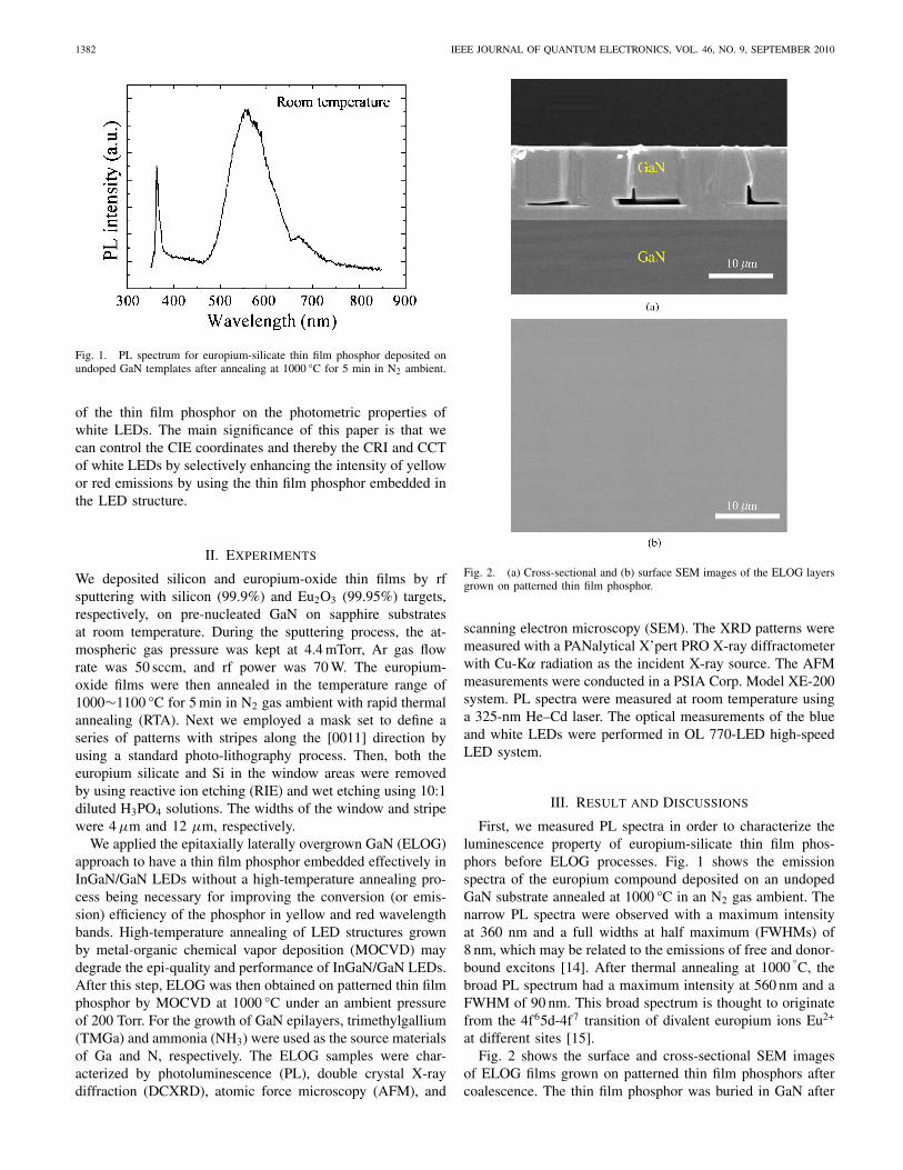
Fig. 1. PL spectrum for europium-silicate thin film phosphor deposited onundoped GaN templates after annealing at 1000 °C for 5 min in N2 ambient.
of the thin film phosphor on the photometric properties ofwhite LEDs. The main significance of this paper is that wecan control the CIE coordinates and thereby the CRI and CCTof white LEDs by selectively enhancing the intensity of yellowor red emissions by using the thin film phosphor embedded inthe LED structure.
II. Experiments
We deposited silicon and europium-oxide thin films by rfsputtering with silicon (99.9%) and Eu2O3 (99.95%) targets,respectively, on pre-nucleated GaN on sapphire substratesat room temperature. During the sputtering process, the at-mospheric gas pressure was kept at 4.4 mTorr, Ar gas flowrate was 50 sccm, and rf power was 70 W. The europium-oxide films were then annealed in the temperature range of1000∼1100 °C for 5 min in N2 gas ambient with rapid thermalannealing (RTA). Next we employed a mask set to define aseries of patterns with stripes along the [0011] direction byusing a standard photo-lithography process. Then, both theeuropium silicate and Si in the window areas were removedby using reactive ion etching (RIE) and wet etching using 10:1diluted H3PO4 solutions. The widths of the window and stripewere 4 µm and 12 µm, respectively.
We applied the epitaxially laterally overgrown GaN (ELOG)approach to have a thin film phosphor embedded effectively inInGaN/GaN LEDs without a high-temperature annealing pro-cess being necessary for improving the conversion (or emis-sion) efficiency of the phosphor in yellow and red wavelengthbands. High-temperature annealing of LED structures grownby metal-organic chemical vapor deposition (MOCVD) maydegrade the epi-quality and performance of InGaN/GaN LEDs.After this step, ELOG was then obtained on patterned thin filmphosphor by MOCVD at 1000 °C under an ambient pressureof 200 Torr. For the growth of GaN epilayers, trimethylgallium(TMGa) and ammonia (NH3) were used as the source materialsof Ga and N, respectively. The ELOG samples were char-acterized by photoluminescence (PL), double crystal X-raydiffraction (DCXRD), atomic force microscopy (AFM), and
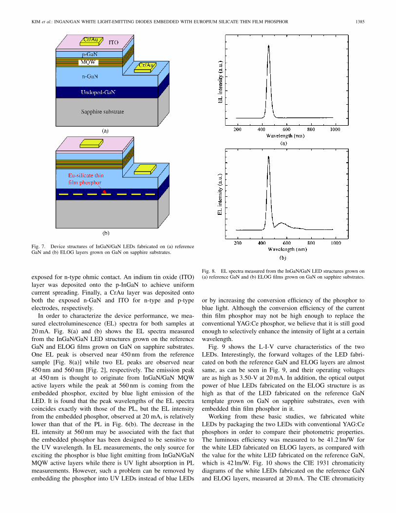
Fig. 2. (a) Cross-sectional and (b) surface SEM images of the ELOG layersgrown on patterned thin film phosphor.
scanning electron microscopy (SEM). The XRD patterns weremeasured with a PANalytical X’pert PRO X-ray diffractometerwith Cu-Kα radiation as the incident X-ray source. The AFMmeasurements were conducted in a PSIA Corp. Model XE-200system. PL spectra were measured at room temperature usinga 325-nm He–Cd laser. The optical measurements of the blueand white LEDs were performed in OL 770-LED high-speedLED system.
III. Result and Discussions
First, we measured PL spectra in order to characterize theluminescence property of europium-silicate thin film phos-phors before ELOG processes. Fig. 1 shows the emissionspectra of the europium compound deposited on an undopedGaN substrate annealed at 1000 °C in an N2 gas ambient. Thenarrow PL spectra were observed with a maximum intensityat 360 nm and a full widths at half maximum (FWHMs) of8 nm, which may be related to the emissions of free and donor-bound excitons [14]. After thermal annealing at 1000 °C, thebroad PL spectrum had a maximum intensity at 560 nm and aFWHM of 90 nm. This broad spectrum is thought to originatefrom the 4f65d-4f7 transition of divalent europium ions Eu2+
at different sites [15].Fig. 2 shows the surface and cross-sectional SEM images
of ELOG films grown on patterned thin film phosphors aftercoalescence. The thin film phosphor was buried in GaN after

KIM et al.: INGAN/GAN WHITE LIGHT-EMITTING DIODES EMBEDDED WITH EUROPIUM SILICATE THIN FILM PHOSPHOR 1383
Fig. 3. 5 × 5 µm2 AFM scan images for (a) reference GaN grown on GaNon sapphire substrates and (b) ELOG grown on patterned thin film phosphor.
3 h of growth, and the surface morphology became smooth.The thickness of the overgrown GaN layer was 8 µm and thethickness of the europium silicate layer was 1.75 mm. Eachblack spot in the overgrown GaN layer shown in Fig. 2(a) is asubsurface void that forms when two growth fronts coalesce.These voids are often observed under lateral growth conditionsin which stripes having vertical side facets develop [16]. AnSEM image of Fig. 2(b) shows that the GaN layer aftercoalescence has a microscopically flat and pit-free surface. Wefurther investigated the surface morphology of ELOG samplesusing AFM and compared them with GaN samples grown onflat thin film phosphor, as shown in Fig. 3(a) and (b). TheAFM image was scanned over 5 × 5 µm2 areas on the (0001)plane, and a microscopically pit-free surface was observedfor both samples. The pits are generally associated with athreading dislocation (TD) [17], and therefore we believe thatthe lateral growth regions are almost free of TD. The root-mean-square (RMS) value of the reference GaN was measuredto be 1.563 nm, compared with values as low as 1.605 nm forthe ELOG sample.
We measured DCXRD to compare the crystalline quality ofthe two samples. Fig. 4 shows double crystal X-ray rockingcurves observed from the (002) and (102) planes for eachsample. Both samples show only one peak, indicating good
Fig. 4. Comparison of X-ray rocking curves, measured from (a) (002) planeand (b) (102) plane, of both the reference GaN grown on GaN on sapphiresubstrates and ELOG grown on patterned thin film phosphor.
epitaxial quality. The FWHMs measured for the (002) planein the reference and ELOG samples were 235 and 249 arcsec,respectively, as shown in Fig. 4(a), whereas those for the(102) plane in the reference and ELOG samples were 405 and416 arcsec, respectively, as shown in Fig. 4(b). Although theFWHMs of the ELOG samples are slightly larger than those ofthe reference samples, the difference is not significant, whichindicates the TD density of the ELOG sample is comparableto that of the reference sample. In general, FWHMs of adiffraction peak are used as an indication of the density ofTD. Next, we again measured the luminescent properties of thepatterned thin film phosphor in order to examine its emissionefficiency after ELOG processes at a target wavelength. Fig. 5shows the PL spectra of the reference GaN and ELOG layersgrown on GaN on sapphire substrates. A narrow PL spectrumwas observed for the reference GaN, with a maximum intensityat 360 nm and a FWHM of 8 nm, as shown in Fig. 5(a),whereas in the ELOG sample, another intense and broademission peak, in addition to the peak with a FWHM of 8 nmat 360 nm, was detected at 550 nm with a FWHM of 90 nm,shown in Fig. 5(b). The narrow peak in the ELOG sample isthought to have the same origin as the peak in the referenceGaN, and the emission peak at 550 nm is thought to originatefrom the 4f65d-4f7 transition of divalent europium ions Eu2+

1384 IEEE JOURNAL OF QUANTUM ELECTRONICS, VOL. 46, NO. 9, SEPTEMBER 2010
Fig. 5. PL spectra of (a) reference GaN grown on GaN on sapphire sub-strates and (b) ELOG grown on patterned thin film phosphor.
in the europium-silicate thin film phosphor, as described inFig. 1 [15].
These results indicate that the proposed ELOG scheme usedfor embedding thin film phosphor into the LED structureworks reasonably well without use of high-temperature anneal-ing processes and thus it can be applied to either replace theconventional YAG phosphor if its intensity is strong enough orenhance the intensity of yellow and red emissions selectivelyalong with YAG phosphor, eventually improving photometricproperties such as the CRI and the CCT of the white LEDswithout sacrificing their crystallinity.
Based on these studies on the ELOG film, we grew epilayersfor InGaN/GaN multiple quantum well (MQW) LEDs on itand measured PL spectra to confirm whether the emissionfrom the thin film phosphor is still strong enough to makewhite light. Fig. 6(a) and (b) shows the PL spectra measuredfrom the InGaN/GaN LED structures grown on the referenceGaN and ELOG films grown on GaN on sapphire substrates.In Fig. 6(a), the little hump at 550 nm in the PL spectra of theELOG sample without europium silicate is observed, whichis thought to be related to yellow defects that are commonlyobserved in GaN. As expected, a strong and broad PL peakwas observed near 550 nm with a FWHM of 90 nm, which isthought to originate from the embedded phosphor, excited byboth UV and blue light emissions, together with a narrow PLpeak at 420 nm, which is likely to come from the InGaN/GaN
Fig. 6. PL spectra measured from the InGaN/GaN LED structures grown on(a) reference GaN and (b) ELOG films grown on GaN on sapphire substrates.
MQW active layers. In general, the absorption coefficient inthe blue spectral range is larger than 2000 cm−1 [18]. The PLpeak of InGaN/GaN LED structures grown on ELOG filmswas shifted to shorter wavelengths as compared to that ofInGaN/GaN LED structures grown on the reference GaN.It is thought to be due to the strain generated during thegrowth of InGaN/GaN MQW active layers on ELOG films.The PL intensity from the thin film phosphor was strongenough to be comparable to more than half of the PL intensityfrom the active layers. Then, we continued to fabricate atop-emitting InGaN/GaN MQW LEDs, and measured lightintensity-current-voltage (L-I-V) characteristics of the twoLEDs fabricated on the reference GaN and ELOG template.
Fig. 7(a) and (b) shows the device structures of In-GaN/GaN LEDs fabricated on the reference GaN and ELOGlayers, grown on GaN on c-plane sapphire substrates. Theeuropium-silicate LED structure was composed of a Si-doped, 8 µm-thick n-type GaN layer embedded with thepatterned thin film phosphor, five-period MQW active layersthat consist of 15 nm-thick In0.01Ga0.99N barriers and 2 nm-thick In0.16Ga0.84N quantum wells, and a Mg-doped 0.14 µmInGaN p-type layer from the bottom. The reference LEDhas the same structure as the europium-silicate LED, exceptfor the patterned thin film phosphor. For the fabrication ofInGaN/GaN MQW LEDs, a 1 µm-depth mesa was formedby inductively coupled plasma RIE and n-GaN was partly
KIM et al.: INGAN/GAN WHITE LIGHT-EMITTING DIODES EMBEDDED WITH EUROPIUM SILICATE THIN FILM PHOSPHOR 1385
Fig. 7. Device structures of InGaN/GaN LEDs fabricated on (a) referenceGaN and (b) ELOG layers grown on GaN on sapphire substrates.
exposed for n-type ohmic contact. An indium tin oxide (ITO)layer was deposited onto the p-InGaN to achieve uniformcurrent spreading. Finally, a CrAu layer was deposited ontoboth the exposed n-GaN and ITO for n-type and p-typeelectrodes, respectively.
In order to characterize the device performance, we mea-sured electroluminescence (EL) spectra for both samples at20 mA. Fig. 8(a) and (b) shows the EL spectra measuredfrom the InGaN/GaN LED structures grown on the referenceGaN and ELOG films grown on GaN on sapphire substrates.One EL peak is observed near 450 nm from the referencesample [Fig. 8(a)] while two EL peaks are observed near450 nm and 560 nm [Fig. 2], respectively. The emission peakat 450 nm is thought to originate from InGaN/GaN MQWactive layers while the peak at 560 nm is coming from theembedded phosphor, excited by blue light emission of theLED. It is found that the peak wavelengths of the EL spectracoincides exactly with those of the PL, but the EL intensityfrom the embedded phosphor, observed at 20 mA, is relativelylower than that of the PL in Fig. 6(b). The decrease in theEL intensity at 560 nm may be associated with the fact thatthe embedded phosphor has been designed to be sensitive tothe UV wavelength. In EL measurements, the only source forexciting the phosphor is blue light emitting from InGaN/GaNMQW active layers while there is UV light absorption in PLmeasurements. However, such a problem can be removed byembedding the phosphor into UV LEDs instead of blue LEDs
Fig. 8. EL spectra measured from the InGaN/GaN LED structures grown on(a) reference GaN and (b) ELOG films grown on GaN on sapphire substrates.
or by increasing the conversion efficiency of the phosphor toblue light. Although the conversion efficiency of the currentthin film phosphor may not be high enough to replace theconventional YAG:Ce phosphor, we believe that it is still goodenough to selectively enhance the intensity of light at a certainwavelength.
Fig. 9 shows the L-I-V curve characteristics of the twoLEDs. Interestingly, the forward voltages of the LED fabri-cated on both the reference GaN and ELOG layers are almostsame, as can be seen in Fig. 9, and their operating voltagesare as high as 3.50-V at 20 mA. In addition, the optical outputpower of blue LEDs fabricated on the ELOG structure is ashigh as that of the LED fabricated on the reference GaNtemplate grown on GaN on sapphire substrates, even withembedded thin film phosphor in it.
Working from these basic studies, we fabricated whiteLEDs by packaging the two LEDs with conventional YAG:Cephosphors in order to compare their photometric properties.The luminous efficiency was measured to be 41.2 lm/W forthe white LED fabricated on ELOG layers, as compared withthe value for the white LED fabricated on the reference GaN,which is 42 lm/W. Fig. 10 shows the CIE 1931 chromaticitydiagrams of the white LEDs fabricated on the reference GaNand ELOG layers, measured at 20 mA. The CIE chromaticity

1386 IEEE JOURNAL OF QUANTUM ELECTRONICS, VOL. 46, NO. 9, SEPTEMBER 2010
Fig. 9. L-I-V characteristics of InGaN/GaN blue LEDs fabricated with GaNon sapphire substrates and with ELOG on patterned thin film phosphor.
Fig. 10. Coordinates of white LEDs with the reference GaN layer and ELOGon patterned thin film phosphor at 20 mA, plotted in the CIE 1931 chromaticitydiagram.
coordinate, the CCT, and the CRI were calculated to be (0.30,0.28), 8467 K, and 66.52, respectively, for the white LEDsfabricated on the reference GaN layers, as compared withthe values for the white LEDs fabricated on ELOG layers,which are (0.33, 0.39), 5607 K, and 77.60, respectively. Here,we found that tristimulus coordinates shift to the red sideof the CIE chromaticity diagram from (0.30, 0.28) to (0.33,0.39), the CCT decreases from 8467 K to 5607 K, and the CRIincreases from 66.52 to 77.60. These changes are thought to becaused by the thin film phosphor with a maximum conversionefficiency at 560 nm, embedded in the InGaN/GaN blue LEDstructure. Further efforts to improve the conversion efficiencyof the thin film phosphor in red emissions will make it moreuseful in solid-state lighting applications.
IV. Conclusion
We used europium-silicate compounds to fabricate a thinfilm phosphor that emits with maximum intensity at 560 nm
and applied this to InGaN/GaN LEDs to examine its effecton the photometric properties of white LEDs. Followingthe ELOG concept we embedded the thin film phosphoreffectively in InGaN/GaN LEDs using MOCVD without ahigh-temperature annealing process; this annealing is typicallyneeded to improve the conversion efficiency of the thin filmphosphor in the yellow or red wavelength bands. After this weused MOCVD to grow epilayers for InGaN/GaN blue LEDs,and we investigated their structural and optical characteristicswith SEM, AFM, DCXRD, and PL measurements. Accordingto AFM observations, the ELOG sample showed no pits onthe surface, and its RMS value was as low as 1.605 nmfor 5 × 5 µm2 areas. We observed the FWHM of the X-rayrocking curves from the (002) and (102) planes of the ELOGsample to be 249 and 416 arcsec, respectively, and the PLspectrum from the thin film phosphor was measured to have amaximum intensity at 550 nm and a FWHM of 90 nm. Finally,we investigated the photometric properties of the white LEDsfabricated on the reference GaN and ELOG layers and foundthat, for those LEDs fabricated on the ELOG layers, the CCThad improved from 8467 K to 5607 K and the CRI had changedfrom 66.52 to 77.60.
References
[1] U. Kaufmann, M. Kunzer, K. Köhler, H. Obloh, W. Pletschen, P.Schlotter, R. Schmidt, J. Wagner, A. Ellens, W. Rossner, and M.Kobusch, “Ultraviolet pumped tricolor phosphor blend white emittingLEDs,” Phys. Status Solidi A, vol. 188, no. 1, pp. 143–146, Nov. 2001.
[2] N. Shibata, T. Uemura, H. Yamaguchi, and T. Yasukawa, “Ultravioletpumped tricolor phosphor blend white emitting LEDs,” Phys. StatusSolidi A, vol. 192, no. 2, pp. 254–260, Aug. 2002.
[3] M. Yamada, Y. Narukawa, and T. Mukai, “Phosphor free high-luminous-efficiency white light-emitting diodes composed of InGaN multiquantumwell,” Jpn. J. Appl. Phys. pt. 2, vol. 41, no. 3A, pp. L246–L248, Mar.2002.
[4] R. Mueller-Mach and G. O. Mueller, “White light emitting diodes forillumination,” in Proc. SPIE, vol. 3938. 2000, pp. 30–40.
[5] G. O. Mueller and R. Mueller-Mach, “Illumination grade white LEDs,”in Proc. SPIE, vol. 4776. 2002, pp. 122–130.
[6] S. Nakamura and G. Fasol, The Blue Laser Diode: GaN Based LightEmitters and Lasers. Heidelberg, Germany: Springer, 1997.
[7] M. R. Krames, O. B. Shchekin, R. Mueller-Mach, G. O. Mueller, L.Zhou, G. Harbers, and M. G. Craford, “Status and future of high-powerlight-emitting diodes for solid-state lighting,” J. Disp. Technol., vol. 3,no. 2, pp. 160–175, 2007.
[8] J. Y. Tsao, “Solid-state lighting: Lamps, chips, and materials for tomor-row,” IEEE Circuits Devices Mag., vol. 20, no. 3, pp. 28–37, May–Jun.2004.
[9] R. Mueller-Mach, G. O. Mueller, M. R. Krames, and T. Trottier, “High-power phosphor-converted light-emitting diodes based on III-nitrides,”IEEE J. Sel. Topics Quantum Electron., vol. 8, no. 2, pp. 339–345,Mar.–Apr. 2002.
[10] R. Mueller-Mach, G. O. Mueller, and M. R. Krames, “Phosphorsmaterials and combinations for illumination grade white pcLED,” inProc. SPIE, vol. 5187. 2004, pp. 115–122.
[11] Y. D. Huk, J. H. Shim, Y. Kim, and Y. R. Do, “Optical properties ofthree-band white light emitting diode,” J. Electrochem. Soc., vol. 150,no. 2, pp. H57–H60, 2003.
[12] J. Zhang, M. Takahashi, Y. Tokuda, and T. Yoko, “Preparation of Eu-doped CaGa S-CaS composite bicolor phosphor for white light emittingdiode,” J. Ceram. Soc. Jpn., vol. 112, no. 9, pp. 511–513, 2004.
[13] J. Bae, K. Shim, B. Moon, S. Kim, J. Jeong, S. Yi, and J. Kim,“Enhanced luminescent characteristics of Y2-xGdxO3:Eu3+ ceramicphosphors by li-doping,” J. Korean Phys. Soc., vol. 46, no. 5, pp. 1193–1197, May 2005.
[14] P. P. Paskov, R. Schifano, T. Paskova, T. Malinauskas, J. P. Bergman,B. Monemar, S. Figge, and D. Hommel, “Structural defect-related

KIM et al.: INGAN/GAN WHITE LIGHT-EMITTING DIODES EMBEDDED WITH EUROPIUM SILICATE THIN FILM PHOSPHOR 1387
emissions in nonpolar a-plane GaN,” Physica B, vol. 376, pp. 473–476,Apr. 2006.
[15] J. Qi, T. Matsumoto, M. Tanaka, and Y. Masumoto, “Electrolumines-cence of europium silicate thin film on silicon,” Appl. Phys. Lett.,vol. 74, pp. 3203–3205, May 1999.
[16] O. Nam, T. Zheleva, M. Bremser, and R. Davis, “Lateral epitaxialovergrowth of GaN films on SiO2 areas via metalorganic vapor phaseepitaxy” J. Electron. Mater., vol. 27, no. 4, pp. 233–237, Apr. 1998.
[17] N. Sharma, P. Thomas, D. Tricker, and C. Humphreys, “Chemicalmapping and formation of V-defects in InGaN multiple quantum wells,”Appl. Phys. Lett., vol. 77, pp. 1274–1276, Aug. 2000.
[18] J. Schones, E. Kaldis, W. Thoni, and P. Wachter, “Optical, mag-netic, and magnetooptical properties of the europium silicate glassEu0.14Si0.31O0.55,” Phys. Stat. Sol. (a), vol. 51, pp. 173–181, Jul.1979.
Eun Hong Kim received the B.S. degree in electronic engineering fromSejong University, Seoul, South Korea, in 2006, and the M.S. degree fromthe School of Electronic Engineering, Korea University, Seoul, in 2009.
He has been involved with thin film deposition since 2006 and hasperformed the Eu silicate thin film phosphor for white LEDs using ELOprocess. He is currently a Research Scientist with the Group of Research andDevelopment, Hynix Semiconductor, Inc., Icheon, Korea. He is working onflash memory devices.
Kyoung Chan Kim received the B.S. and M.S. degrees in electronic materialengineering from Kwangwoon University, Seoul, Korea, in 2003 and 2005,respectively. He is currently working toward the Ph.D. degree in electronicengineering from the Advanced Semiconductor Laboratory, Korea University,Seoul, Korea.
His current research interests include design and fabrication of optical andelectronic devices having quantum structure.
Dong Ho Kim received the B.S. and M.S. degrees in electronic materialsengineering from Kwangwoon University, Seoul, Korea, in 2004 and 2006,respectively. He is currently working toward the Ph.D. degree in compoundsemiconductor based electronic devices from the Advanced SemiconductorLaboratory, School of Electronics and Electrical Engineering, Korea Univer-sity, Seoul.
His current research interests include device design and fabrication ofgallium-nitride optoelectronic devices.
Jong Hyeob Baek received the B.S., M.S., and Ph.D. degrees in materialsscience and engineering from Korea University in 1989, 1991, and 1999,respectively.
He was a Senior Research Staff Member with the Electronics and Telecom-munications Research Institute working on the epitaxial growth of verticalcavity surface emitting lasers from 1991 to 1999. He was a Post-DoctoralFellow with University of California, San Diego. Since 2002, he has beenwith the Korea Photonics Technology Institute, Gwangju, Korea, where he hasbeen working on the advanced epi/chip technologies of high-efficiency, high-power R/G/B/UV LED, mainly focusing on nano based fabrication process,wafer level packaging process, and high ESD electrode design.
Tae Geun Kim received the B.S., M.S., and Ph.D. degrees in electronicsengineering from Korea University, Seoul, Korea, in 1990, 1993, and 1997,respectively.
After graduation, he was with the Department of Electrical and ComputerEngineering, University of California, San Diego, as a Post-Doctoral Fellow,with the Electron Device Division, Electrotechnical Laboratory, Japan, as aNew Energy and Industrial Technology Development Organization Fellow, andwith the Material Device Laboratory, Samsung Advanced Institute of Tech-nology, Calgary, AB, Canada, as a Principal Research Scientist from 1997 to2002. He has been a Professor in the Department of Electronics Engineering,Korea University, Seoul, since then. His current research interests includesemiconductor materials and devices, semiconductor quantum structures andtheir applications to lasers and memories.