LECTURE NOTESvemu.org/uploads/lecture_notes/03_01_2020_65460003.pdfDepartment of Electrical and...
106
Subject code:15A02503 Power Electronics DEPT.OF EEE VEMUIT Page 1 LECTURE NOTES ON POWER ELECTRONICS III B. Tech I Semester (JNTUA-R15) Dr.D.CHANDRA SEKHAR, M.TECH,P.hD,MISTE. PROFESSOR, HOD,EEE. Department of Electrical and Electronics Engineering VEMU INSTITUTE OF TECHNOLOGY::P.KOTHAKOTA NEAR PAKALA, CHITTOOR-517112 (Approved by AICTE, New Delhi & Affiliated to JNTUA, Anantapuramu)
Transcript of LECTURE NOTESvemu.org/uploads/lecture_notes/03_01_2020_65460003.pdfDepartment of Electrical and...
Subject code:15A02503 Power Electronics
DEPT.OF EEE VEMUIT Page 1
LECTURE NOTES
ON
POWER ELECTRONICS
III B. Tech I Semester (JNTUA-R15)
Dr.D.CHANDRA SEKHAR, M.TECH,P.hD,MISTE.
PROFESSOR, HOD,EEE.
Department of Electrical and Electronics Engineering VEMU INSTITUTE OF TECHNOLOGY::P.KOTHAKOTA
NEAR PAKALA, CHITTOOR-517112
(Approved by AICTE, New Delhi & Affiliated to JNTUA, Anantapuramu)

Subject code:15A02503 Power Electronics
DEPT.OF EEE VEMUIT Page 2
SYLLABUS
UNIT I: POWER SEMI CONDUCTOR DEVICES
Semiconductor Power Diodes, Thyristors – Silicon Controlled Rectifiers (SCR’s) – TRIACs, GTOs -
Characteristics and Principles of Operation and other Thyristors – Classification of Switching Devices
Based on Frequency and Power Handling Capacity-BJT – Power Transistor - Power MOSFET – Power
IGBT -– Basic Theory of Operation of SCR – Static Characteristics – Turn On and Turn Off Methods-
Dynamic Characteristics of SCR - Two Transistor Analogy – Triggering Circuits––– Series and Parallel
Connections of SCR’s – Snubber Circuits – Specifications and Ratings of SCR’s, BJT, IGBT.
UNIT II: PHASE CONTROLLED CONVERTERS
Phase Control Technique – Single Phase Line Commutated Converters – Mid Point and Bridge
Connections – Half Controlled Converters, Fully Controlled Converters with Resistive, RL Loads and
RLE Load– Derivation of Average Load Voltage and Current – Line Commutated Inverters -Active and
Reactive Power Inputs to the Converters without and with Free Wheeling Diode, Effect of Source
Inductance – Numerical Problems. Three Phase Line Commutated Converters – Three Pulse and Six
Pulse Converters – Mid Point and Bridge Connections - Average Load Voltage with R and RL Loads –
Effect of Source Inductance–Dual Converters (Both Single Phase and Three Phase) - Waveforms –
Numerical Problems.
UNIT III: CHOPPERS AND REGULATORS
Commutation Circuits – Time Ratio Control and Current Limit Control Strategies – Step Down and Step
up Choppers Derivation of Load Voltage and Currents with R, RL and RLE Loads- Step Up Chopper –
Load Voltage Expression– Problems. Study of Buck, Boost and Buck-Boost regulators, buck regulator
TPS54160, hysteretic buck regulator e.g.LM3475, Switching Regulator and characteristics of standard
regulator ICs – TPS40200, TPS40210, TPS 7A4901, TPS7A8300
UNIT IV: INVERTERS
Inverters – Single Phase Inverter – Basic Series Inverter – Basic Parallel Capacitor Inverter Bridge
Inverter – Waveforms – Simple Forced Commutation Circuits for Bridge Inverters – Single Phase Half
and Full Bridge Inverters-Pulse Width Modulation Control-Harmonic Reduction Techniques-Voltage
Control Techniques for Inverters – Numerical Problems, Three Phase VSI in 1200 And 1800 Modes of
Conduction.
UNIT V: AC VOLTAGE CONTROLLERS & CYCLO CONVERTERS
AC Voltage Controllers – Single Phase Two SCR’s in Anti Parallel – With R and RL Loads – Modes of
Operation of TRIAC – TRIAC with R and RL Loads – Derivation of RMS Load Voltage, Current and
Power Factor Wave Forms – Firing Circuits -Numerical Problems - Thyristor Controlled Reactors;
Switched Capacitor Networks.
Cyclo Converters – Single Phase Mid Point Cycloconverters with Resistive and Inductive Load
(Principle of Operation only) – Bridge Configuration of Single Phase Cycloconverter (Principle of
Operation only) – Waveforms
.
TEXT BOOKS:
1. Power Electronics, M. D. Singh and K. B. Khanchandani, Mc Graw Hill Education (India) Pvt.
Ltd., 2nd Edition, 2007, 23rd Reprint 2015.
2. Power Electronics: Circuits, Devices and Applications, Muhammad H. Rashid, Pearson, 3rd
Edition, 2014, 2nd Impression 2015.
REFERENCE BOOKS:

Subject code:15A02503 Power Electronics
DEPT.OF EEE VEMUIT Page 3
1. Power Electronics, K. R. Varmah, Chikku Abraham, CENGAGE Learning, 1st Edition, 2016.
2. Power Electronics, P. S. Bimbhra, Khanna Publishers, 2012.
3. Power Electronics: Devices, Circuits, and Industrial Applications, V. R. Moorthi, OXFORD
University Press, 1st Edition, 2005, 12th Impression 2012.
Subject code:15A02503 Power Electronics
DEPT.OF EEE VEMUIT Page 4
UNIT-I
POWER SEMICONDUCTOR DEVICES
Subject code:15A02503 Power Electronics
DEPT.OF EEE VEMUIT Page 5
Main power source
Power
Electronic
circuit
Load
POWER ELECTRONICS
The control of electric motor drives requires control of electric power. Power electronics have
eased the concept of power control. Power electronics signifies the word power electronics
and control or we can say the electronic that deal with power equipment for power control.
Ref signal
Power electronics based on the switching of power semiconductor devices. With the
development of power semiconductor technology, the power handling capabilities and
switching speed of power devices have been improved tremendously.
Power Semiconductor Devices
The first SCR was developed in late 1957. Power semiconductor devices are broadly
categorized into 3 types:
1. Power diodes (600V,4500A)
2. Transistors
3. Thyristors (10KV,300A,30MW)
Thyristor is a four layer three junction pnpn semiconductor switching device. It has 3
terminals these are anode, cathode and gate. SCRs are solid state device, so they are compact,
possess high reliability and have low loss.
Control
Circuit
Feedback Signal
Digital
Circuit
Subject code:15A02503 Power Electronics
DEPT.OF EEE VEMUIT Page 6
SCR is made up of silicon, it act as a rectifier; it has very low resistance in the forward
direction and high resistance in the reverse direction. It is a unidirectional device.
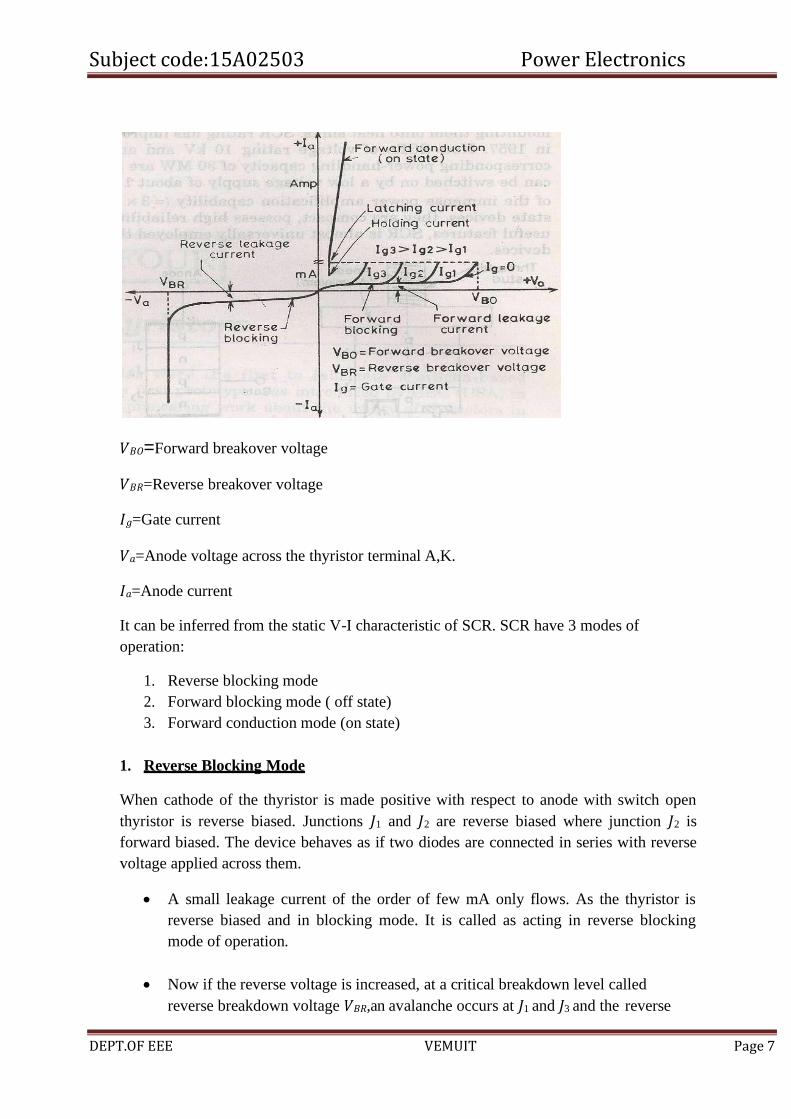
Static V-I characteristics of a Thyristor
The circuit diagram for obtaining static V-I characteristics is as shown
Anode and cathode are connected to main source voltage through the load. The gate and
cathode are fed from source 𝐸𝑆.
A typical SCR V-I characteristic is as shown below:
Subject code:15A02503 Power Electronics
DEPT.OF EEE VEMUIT Page 7
𝑉𝐵𝑂=Forward breakover voltage
𝑉𝐵𝑅=Reverse breakover voltage
𝐼𝑔=Gate current
𝑉𝑎=Anode voltage across the thyristor terminal A,K.
𝐼𝑎=Anode current
It can be inferred from the static V-I characteristic of SCR. SCR have 3 modes of
operation:
1. Reverse blocking mode
2. Forward blocking mode ( off state)
3. Forward conduction mode (on state)
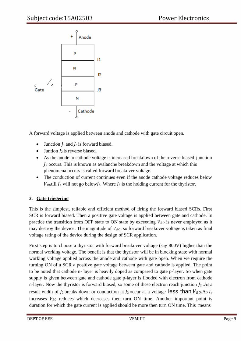
1. Reverse Blocking Mode
When cathode of the thyristor is made positive with respect to anode with switch open
thyristor is reverse biased. Junctions 𝐽1 and 𝐽2 are reverse biased where junction 𝐽2 is
forward biased. The device behaves as if two diodes are connected in series with reverse
voltage applied across them.
• A small leakage current of the order of few mA only flows. As the thyristor is
reverse biased and in blocking mode. It is called as acting in reverse blocking
mode of operation.
• Now if the reverse voltage is increased, at a critical breakdown level called
reverse breakdown voltage 𝑉𝐵𝑅,an avalanche occurs at 𝐽1 and 𝐽3 and the reverse

Subject code:15A02503 Power Electronics
DEPT.OF EEE VEMUIT Page 8
current increases rapidly. As a large current associated with 𝑉𝐵𝑅 and hence more
losses to the SCR.
This results in Thyristor damage as junction temperature may exceed its maximum
temperature rise.
2. Forward Blocking Mode
When anode is positive with respect to cathode, with gate circuit open, thyristor is said to
be forward biased.
Thus junction 𝐽1 and 𝐽3 are forward biased and 𝐽2 is reverse biased. As the forward voltage
is increases junction 𝐽2 will have an avalanche breakdown at a voltage called forward
breakover voltage𝑉𝐵𝑂. When forward voltage is less then 𝑉𝐵𝑂thyristor offers high
impedance. Thus a thyristor acts as an open switch in forward blocking mode.
3. Forward Conduction Mode
Here thyristor conducts current from anode to cathode with a very small voltage drop
across it. So a thyristor can be brought from forward blocking mode to forward
conducting mode:
1. By exceeding the forward breakover voltage.
2. By applying a gate pulse between gate and cathode.
During forward conduction mode of operation thyristor is in on state and behave like a
close switch. Voltage drop is of the order of 1 to 2mV. This small voltage drop is due to
ohmic drop across the four layers of the device.
Different turn ON methods for SCR
1. Forward voltage triggering
2. Gate triggering
3. 𝑑𝑣
triggering 𝑑𝑡
4. Light triggering
5. Temperature triggering
1. Forward voltage triggering
Subject code:15A02503 Power Electronics
DEPT.OF EEE VEMUIT Page 9
A forward voltage is applied between anode and cathode with gate circuit open.
• Junction 𝐽1 and 𝐽3 is forward biased.
• Juntion 𝐽2 is reverse biased.
• As the anode to cathode voltage is increased breakdown of the reverse biased junction
𝐽2 occurs. This is known as avalanche breakdown and the voltage at which this
phenomena occurs is called forward breakover voltage.
• The conduction of current continues even if the anode cathode voltage reduces below
𝑉𝐵𝑂till 𝐼𝑎 will not go below𝐼ℎ. Where 𝐼ℎ is the holding current for the thyristor.
2. Gate triggering
This is the simplest, reliable and efficient method of firing the forward biased SCRs. First
SCR is forward biased. Then a positive gate voltage is applied between gate and cathode. In
practice the transition from OFF state to ON state by exceeding 𝑉𝐵𝑂 is never employed as it
may destroy the device. The magnitude of 𝑉𝐵𝑂, so forward breakover voltage is taken as final
voltage rating of the device during the design of SCR application.
First step is to choose a thyristor with forward breakover voltage (say 800V) higher than the
normal working voltage. The benefit is that the thyristor will be in blocking state with normal
working voltage applied across the anode and cathode with gate open. When we require the
turning ON of a SCR a positive gate voltage between gate and cathode is applied. The point
to be noted that cathode n- layer is heavily doped as compared to gate p-layer. So when gate
supply is given between gate and cathode gate p-layer is flooded with electron from cathode
n-layer. Now the thyristor is forward biased, so some of these electron reach junction 𝐽2 .As a
result width of 𝐽2 breaks down or conduction at 𝐽2 occur at a voltage less than 𝑉𝐵𝑂.As 𝐼𝑔
increases 𝑉𝐵𝑂 reduces which decreases then turn ON time. Another important point is
duration for which the gate current is applied should be more then turn ON time. This means
Subject code:15A02503 Power Electronics
DEPT.OF EEE VEMUIT Page 10
that if the gate current is reduced to zero before the anode current reaches a minimum value
known as holding current, SCR can’t turn ON.
In this process power loss is less and also low applied voltage is required for triggering.
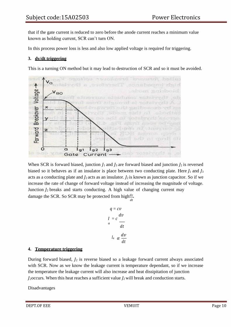
3. dv/dt triggering
This is a turning ON method but it may lead to destruction of SCR and so it must be avoided.
When SCR is forward biased, junction 𝐽1 and 𝐽3 are forward biased and junction 𝐽2 is reversed
biased so it behaves as if an insulator is place between two conducting plate. Here 𝐽1 and 𝐽3
acts as a conducting plate and 𝐽2 acts as an insulator. 𝐽2 is known as junction capacitor. So if we
increase the rate of change of forward voltage instead of increasing the magnitude of voltage.
Junction 𝐽2 breaks and starts conducting. A high value of changing current may
damage the SCR. So SCR may be protected from high𝑑𝑣. 𝑑𝑡
𝑞 = 𝑐𝑣
𝐼 = 𝑐 𝑑𝑣
4. Temperature triggering
𝑎
𝐼𝑎
𝑑𝑡
𝛼 𝑑𝑣
𝑑𝑡
During forward biased, 𝐽2 is reverse biased so a leakage forward current always associated
with SCR. Now as we know the leakage current is temperature dependant, so if we increase
the temperature the leakage current will also increase and heat dissipitation of junction
𝐽2occurs. When this heat reaches a sufficient value 𝐽2 will break and conduction starts.
Disadvantages

Subject code:15A02503 Power Electronics
DEPT.OF EEE VEMUIT Page 11
This type of triggering causes local hot spot and may cause thermal run away of the device.
This triggering cannot be controlled easily.
It is very costly as protection is costly.
5. Light triggering
First a new recess niche is made in the inner p-layer. When this recess is irradiated, then free
charge carriers (electron and hole) are generated. Now if the intensity is increased above a
certain value then it leads to turn ON of SCR. Such SCR are known as Light activated SCR
(LASCR).
Some definitions:
Latching current
The latching current may be defined as the minimum value of anode current which at must
attain during turn ON process to maintain conduction even if gate signal is removed.
Holding current
It is the minimum value of anode current below which if it falls, the SCR will turn OFF.
Switching characteristics of thyristors
The time variation of voltage across the thyristor and current through it during turn on
and turn off process gives the dynamic or switching characteristic of SCR.
Switching characteristic during turn on
Turn on time
It is the time during which it changes from forward blocking state to ON state. Total turn
on time is divided into 3 intervals:
1. Delay time
2. Rise time
3. Spread time
Delay time
If 𝐼𝑔and 𝐼𝑎 represent the final value of gate current and anode current. Then the delay time
can be explained as time during which the gate current attains 0.9 𝐼𝑔 to the instant anode
current reaches 0.1 𝐼𝑔 or the anode current rises from forward leakage current to 0.1 𝐼𝑎.
1. Gate current 0.9 𝐼𝑔 to 0.1 𝐼𝑎.
2. Anode voltage falls from 𝑉𝑎 to 0.9𝑉𝑎.
3. Anode current rises from forward leakage current to 0.1 𝐼𝑎.
Subject code:15A02503 Power Electronics
DEPT.OF EEE VEMUIT Page 12
Rise time (𝒕𝒓)
Time during which
1. Anode current rises from 0.1 𝐼𝑎 to 0.9 𝐼𝑎
2. Forward blocking voltage falls from 0.9𝑉𝑎 to 0.1𝑉𝑎. 𝑉𝑎 is the initial forward blocking
voltage.
Spread time (𝒕𝒑)
1. Time taken by the anode current to rise from 0.9𝐼𝑎 to𝐼𝑎.
2. Time for the forward voltage to fall from 0.1𝑉𝑜 to on state voltage drop of 1 to 1.5V.
During turn on, SCR is considered to be a charge controlled device. A certain amount
of charge is injected in the gate region to begin conduction. So higher the magnitude
of gate current it requires less time to inject the charges. Thus turn on time is reduced
by using large magnitude of gate current.
How the distribution of charge occurs?
As the gate current begins to flow from gate to cathode with the application of gate
signal. Gate current has a non uniform distribution of current density over the cathode
surface. Distribution of current density is much higher near the gate. The density decrease
as the distance from the gate increases. So anode current flows in a narrow region near
gate where gate current densities are highest. From the beginning of rise time the anode
current starts spreading itself. The anode current spread at a rate of 0.1mm/sec. The
spreading anode current requires some time if the rise time is not sufficient then the anode
current cannot spread over the entire region of cathode. Now a large anode current is
applied and also a large anode current flowing through the SCR. As a result turn on losses
is high. As these losses occur over a small conducting region so local hot spots may form
and it may damage the device.
Switching Characteristics During Turn Off
Thyristor turn off means it changed from ON to OFF state. Once thyristor is oON there is
no role of gate. As we know thyristor can be made turn OFF by reducing the anode
current below the latching current. Here we assume the latching current to be zero
ampere. If a forward voltage is applied across the SCR at the moment it reaches zero then
SCR will not be able to block this forward voltage. Because the charges trapped in the 4-
layer are still favourable for conduction and it may turn on the device. So to avoid such a
case, SCR is reverse biased for some time even if the anode current has reached to zero.
So now the turn off time can be different as the instant anode current becomes zero to the
instant when SCR regains its forward blocking capability.
𝑡𝑞 =𝑡𝑟𝑟+𝑡𝑞𝑟 Where,

Subject code:15A02503 Power Electronics
DEPT.OF EEE VEMUIT Page 13
𝑡𝑞 is the turn off time,𝑡𝑟𝑟 is the reverse recovery time, 𝑡𝑞𝑟 is the gate recovery time
At 𝑡1 anode current is zero. Now anode current builds up in reverse direction with same 𝑑𝑣
slope. This is due to the presence of charge carriers in the four layers. The reverse 𝑑𝑡
recovery current removes the excess carriers from 𝐽1 and 𝐽3 between the instants 𝑡1 and𝑡3. At
instant 𝑡3 the end junction 𝐽1 and 𝐽3 is recovered. But 𝐽2 still has trapped charges which decay
due to recombination only so the reverse voltage has to be maintained for some more
time. The time taken for the recombination of charges between 𝑡3 and 𝑡4 is called gate
recovery time 𝑡𝑞𝑟. Junction 𝐽2 recovered and now a forward voltage can be applied across
SCR.
The turn off time is affected by:
1. Junction temperature
2. Magnitude of forward current 𝑑𝑖 during commutation. 𝑑𝑡
Turn off time decreases with the increase of magnitude of reverse applied voltage.
GTO(Gate turn off thyristor)
Subject code:15A02503 Power Electronics
DEPT.OF EEE VEMUIT Page 14
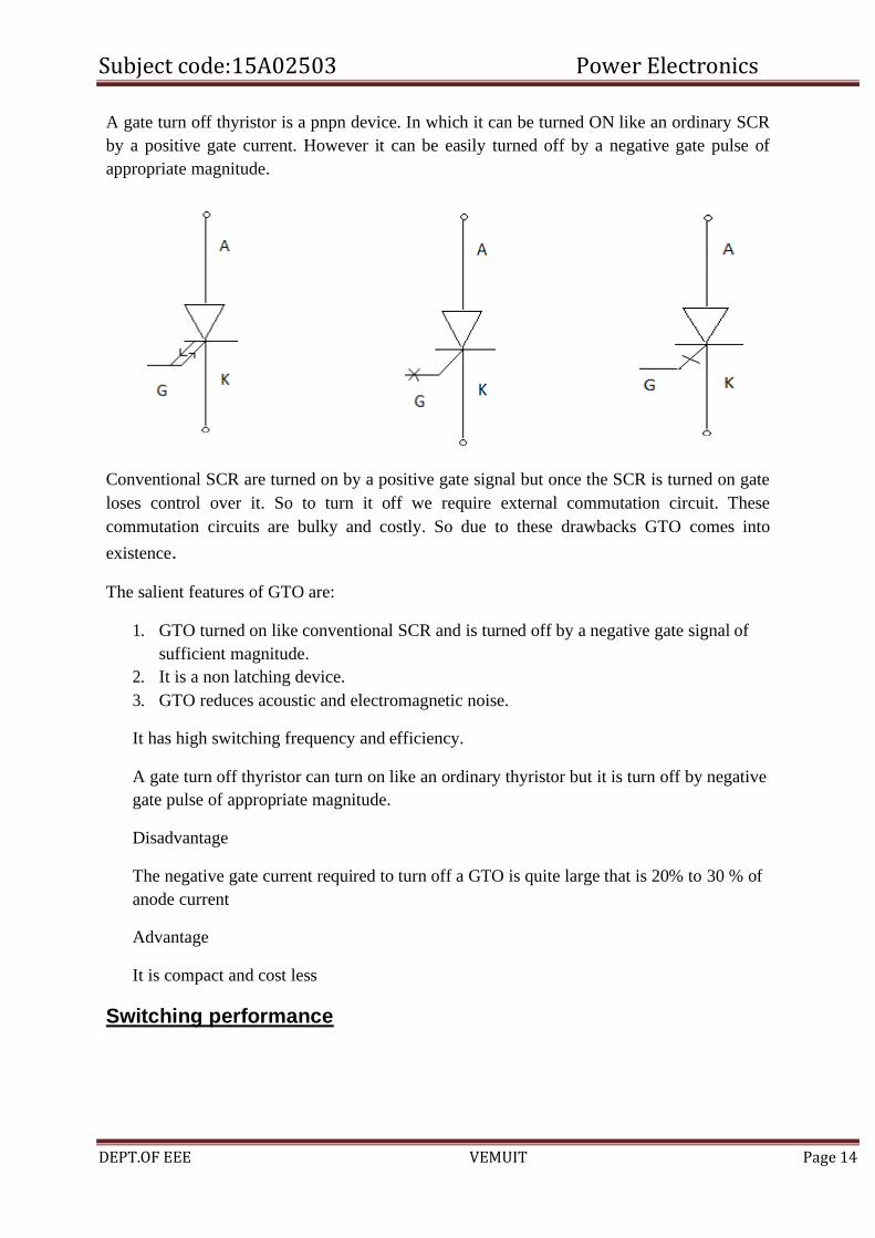
A gate turn off thyristor is a pnpn device. In which it can be turned ON like an ordinary SCR
by a positive gate current. However it can be easily turned off by a negative gate pulse of
appropriate magnitude.
Conventional SCR are turned on by a positive gate signal but once the SCR is turned on gate
loses control over it. So to turn it off we require external commutation circuit. These
commutation circuits are bulky and costly. So due to these drawbacks GTO comes into
existence.
The salient features of GTO are:
1. GTO turned on like conventional SCR and is turned off by a negative gate signal of
sufficient magnitude.
2. It is a non latching device.
3. GTO reduces acoustic and electromagnetic noise.
It has high switching frequency and efficiency.
A gate turn off thyristor can turn on like an ordinary thyristor but it is turn off by negative
gate pulse of appropriate magnitude.
Disadvantage
The negative gate current required to turn off a GTO is quite large that is 20% to 30 % of
anode current
Advantage
It is compact and cost less
Switching performance
Subject code:15A02503 Power Electronics
DEPT.OF EEE VEMUIT Page 15
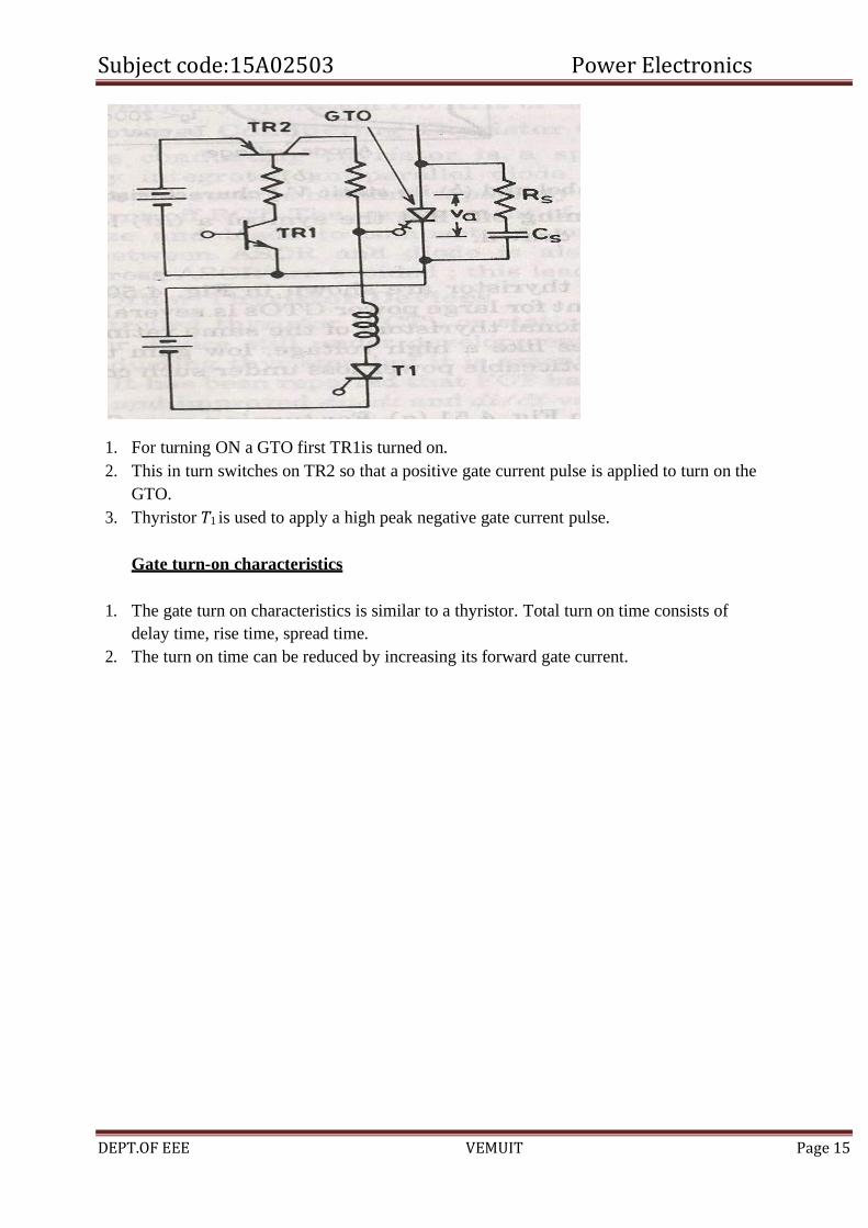
1. For turning ON a GTO first TR1is turned on.
2. This in turn switches on TR2 so that a positive gate current pulse is applied to turn on the
GTO.
3. Thyristor 𝑇1 is used to apply a high peak negative gate current pulse.
Gate turn-on characteristics
1. The gate turn on characteristics is similar to a thyristor. Total turn on time consists of
delay time, rise time, spread time.
2. The turn on time can be reduced by increasing its forward gate current.
Subject code:15A02503 Power Electronics
DEPT.OF EEE VEMUIT Page 16
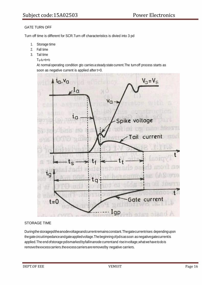
GATE TURN OFF
Turn off time is different for SCR.Turn off characteristics is divied into 3 pd
1. Storage time
2. Fall time
3. Tail time
Tq=ts+tf+tt
At normal operating condition gto carries a steady state current.The turn off process starts as
soon as negative current is applied after t=0.
STORAGE TIME
During the storagepd the anode voltage and current remains constant.The gate current rises depending upon
the gate circuit impedance and gate applied voltage.The beginning of pd is as soon as negative gate current is
applied.The end of storage pd is marked by fall in anode current and rise in voltage,what we have to do is
remove the excess carriers.the excess carriers are removed by negative carriers.
Subject code:15A02503 Power Electronics
DEPT.OF EEE VEMUIT Page 17
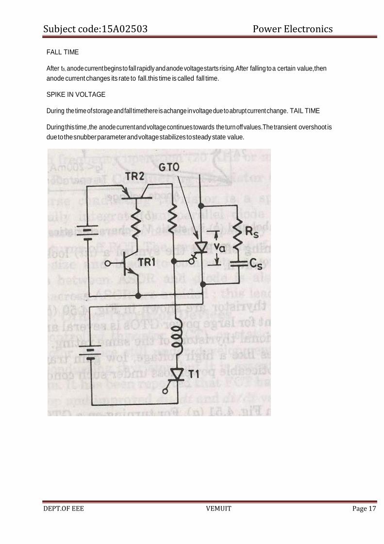
FALL TIME
After ts, anode current begins to fall rapidly and anode voltage starts rising.After falling to a certain value,then
anode current changes its rate to fall.this time is called fall time.
SPIKE IN VOLTAGE
During the time of storage and fall timethere is achange in voltage due to abrupt current change. TAIL TIME
During this time ,the anode current and voltage continues towards the turn off values.The transient overshoot is
due to the snubber parameter and voltage stabilizes to steady state value.
Subject code:15A02503 Power Electronics
DEPT.OF EEE VEMUIT Page 18
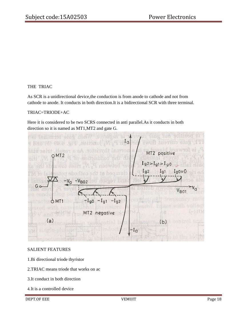
THE TRIAC
As SCR is a unidirectional device,the conduction is from anode to cathode and not from
cathode to anode. It conducts in both direction.It is a bidirectional SCR with three terminal.
TRIAC=TRIODE+AC
Here it is considered to be two SCRS connected in anti parallel.As it conducts in both
direction so it is named as MT1,MT2 and gate G.
SALIENT FEATURES
1.Bi directional triode thyristor
2.TRIAC means triode that works on ac
3.It conduct in both direction
4. It is a controlled device
Subject code:15A02503 Power Electronics
DEPT.OF EEE VEMUIT Page 19
5. Its operation is similar to two devices connected in anti parallel with common gate
connection.
6. It has 3 terminals MT1,MT2 and gate G
Its use is control of power in ac.
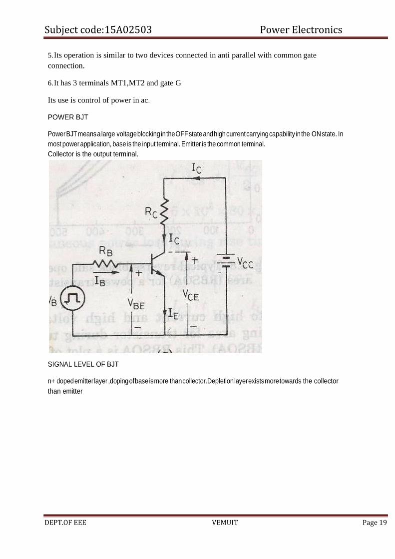
POWER BJT
Power BJT means a large voltage blocking in the OFF state and high current carrying capability in the ON state. In
most power application, base is the input terminal. Emitter is the common terminal.
Collector is the output terminal.
SIGNAL LEVEL OF BJT
n+ doped emitter layer ,doping of base is more than collector.Depletion layer exists more towards the collector
than emitter
Subject code:15A02503 Power Electronics
DEPT.OF EEE VEMUIT Page 20
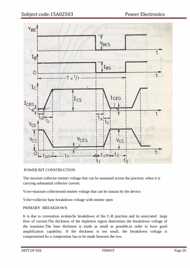
POWER BJT CONSTRUCTION
The maxium collector emitter voltage that can be sustained across the junction, when it is
carrying substantial collector current.
Vceo=maxium collectorand emitter voltage that can be sustain by the device.
Vcbo=collector base breakdown voltage with emitter open
PRIMARY BREAKDOWN
It is due to convention avalanche breakdown of the C-B junction and its associated large
flow of current.The thickness of the depletion region determines the breakdown voltage of
the transistor.The base thickness is made as small as possible,in order to have good
amplification capability. If the thickness is too small, the breakdown voltage is
compromised.So a compromise has to be made between the two.
Subject code:15A02503 Power Electronics
DEPT.OF EEE VEMUIT Page 21
THE DOPING LEVELS-
1.The doping of the emitter layer is quite large.
2.The base doping is moderate.
3.n- region is lightly doped.
4.n+ region doping level is similar to emitter.
1.THICKNESS OF DRIFT REGION-
It determines the breakdown length of the transistor.
2.THE BASE THICKNES –
Small base thickness- good amplification capability
Too small base thickness- the breakdown voltage of the transistor has ti be compromised.
For a relatively thick base,the current gain will be relatively small.so it is increase the
gain.Monolithicesigns for darlington connected BJT pair have been deveploed.
SECONDARY BREAKDOWN
Secondary breakdown is due to large power disspation at localized site within the semi
conductor.
PHYSICS OF BJT OPERATION-
The transistor is assumed to operate in active region. There is no doped collector drift
region. It has importance only in switching operation, in active region of operation.
junction is forward biased and C-B junction is reverse biased. Electrons are injected
into base from the emitter. Holes are injected from base into the emitter.
QUASI SATURATION-
Intially we assume that, the transistor is in active region. Base current is allowed to increase
then lets see what happens.first collector rises in response to base current.So there is a
increase voltage drop across the collector load.So C-E voltage drops.
Because of increase in collector current, there is a increase in voltage in drift region. This
eventually reduces the reverse biased across the C-B junction.so n-p junction get
smaller, at some point the junction become forward bised. So now injection of holes from
base into collector drift region occurs. Charge neutrality requires the electron to be injected
in the drift region of the holes. From where these electron came. Since a large no of
electron is supplied to the C-B junction via injection from emitter and subsequent
diffusion across the base. As excess carrier build up in the drift region begins to occur
quasi saturation region is entered. As the injected carrires increase in the drift region is

Subject code:15A02503 Power Electronics
DEPT.OF EEE VEMUIT Page 22
gradually shotred out and the voltage across the drift region drops. In quasi saturation the
drift region is not completely shorted out by high level injection.Hard saturation obtained
when excess carrier density reaches the n+ side.
During quasi saturation, the rate of the collector fall.Hard saturation occurs when excess
carriers have completely swept across the drift region .
THYRISTOR PROTECTION
OVER VOLTAGE PROTECTION
Over voltage occurring during the switching operation causes the failure of SCR.
INTERNAL OVERVOLTAGE
It is due to the operating condition of SCR.

Subject code:15A02503 Power Electronics
DEPT.OF EEE VEMUIT Page 23
During the commutation of SCR ,when the anode current decays to zero anode current
reverses due to stored changes. First the reverse current rises to peak value, then reverse
current reduces abruptly with large 𝑑𝑖⁄𝑑𝑡. During series inductance of SCR large
transient large voltage i.e 𝐿 𝑑𝑖⁄𝑑𝑡. is generated.
EXTERNAL OVER VOLTAGE
This is due to external supply and load condition. This is because of
1. The interruption of current flow in an inductive circuit.
2. Lightening strokes on the lines feeding the thyristor systems.
Suppose a SCR converter is fed from a transformer, voltage transient occur when
transformer primary will energise or de-energised.
This overvoltages cause random turn ON of a SCR.
The effect of overvoltage is minimized using
1. RC circuits
2. Non linear resistor called voltage clamping device.
Voltage clamping device is a non linear resistor.It is connected between
cathode and anode of SCR. The resistance of voltage clamping device
decreases with increasing voltages. During normal working condition Voltage
clamping (V.C) device has high resistance, drawing only leakage current.
When voltage surge appears voltage clamping device offers a low resistance and it
create a virtual short circuit across the SCR. Hence voltage across SCR is
clamped to a safe value.
Subject code:15A02503 Power Electronics
DEPT.OF EEE VEMUIT Page 24
When surge condition over voltage clamping device returns to high resistance
state.
e.g. of voltage clamping device
1.Seleniumthyrector diodes
2.Metal Oxide varistors
3.Avalanche diode supressors
OVER CURRENT PROTECTION
Long duration operation of SCR, during over current causes the
1.junction temp. of SCR to rise above the rated value,causing permanent
damage to device.
SCR is protected from overcurrent by using
1.Circuit breakers
2.Fast acting fuses
Proper co-ordination is essential because
1..fault current has to be interrupted before SCR gets damaged.
2.only faulty branches of the network has to be replaced.
In stiff supply network,source has negligible impedance.So in such system
the magnitude and rate of rise of current is not limited.Fault current hence
junction temp rises in a few miliseconds.
POINTS TO BE NOTED-
1. Proper coordination between fast acting fuse and thyristor is essential.
2. The fuse is always rated to carry marginal overload current over
definite period.
3. The peak let through current through SCR must be less than sub cycle
rating of the SCR.
4. The voltage across the fuse during arcing time is called arcing or
recovery voltage and is equal to sum of the source voltage and emf
induced in the circuit inductance during arcing time.
5. On abrupt interruption of fuse current, induce emf would be high, which
results in high arcing voltage.
Circuit Breaker (C.B)
has long tripping time. So it is used for protecting the device against continuous
overload current or against the surge current for long duration. In order that fuse
protects the thyristor realiably the 𝐼2𝑡 rating of fuse current must be less than that of
SCR.
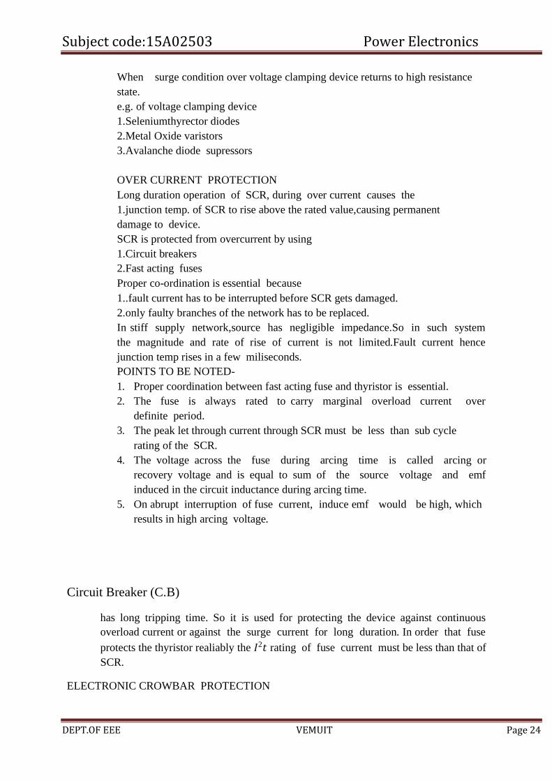
ELECTRONIC CROWBAR PROTECTION
Subject code:15A02503 Power Electronics
DEPT.OF EEE VEMUIT Page 25
For overcurrent protection of power converter using SCR, electronic crowbar are
used. It provide rapid isolation of power converter before any damage occurs.
HEAT PROTECTION- To protect the SCR
1. From the local spots
2. Temp rise
SCRs are mounted over heat sinks.
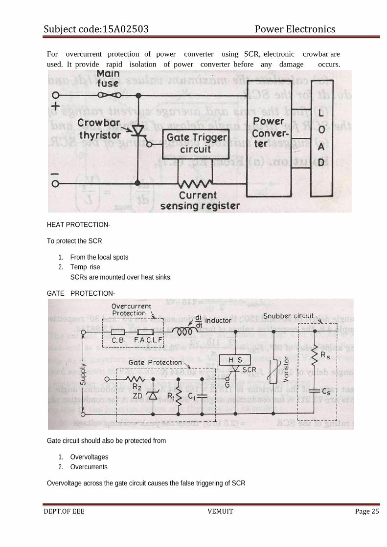
GATE PROTECTION-
Gate circuit should also be protected from
1. Overvoltages
2. Overcurrents Overvoltage across the gate circuit causes the false triggering of SCR
Subject code:15A02503 Power Electronics
DEPT.OF EEE VEMUIT Page 26
Overcurrent raise the junction temperature. Overvoltage protection is by zener diode across
the gate circuit.
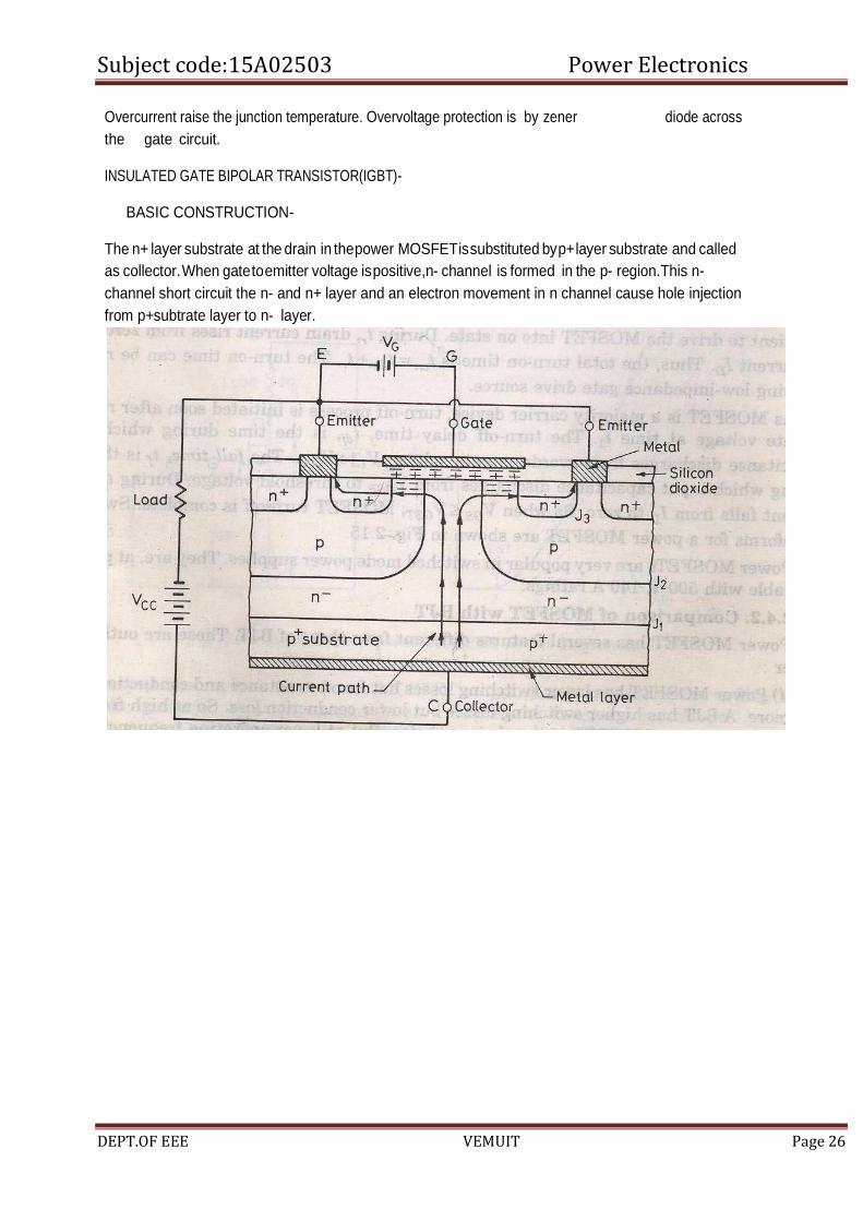
INSULATED GATE BIPOLAR TRANSISTOR(IGBT)-
BASIC CONSTRUCTION-
The n+ layer substrate at the drain in the power MOSFET is substituted by p+ layer substrate and called
as collector. When gate to emitter voltage is positive,n- channel is formed in the p- region.This n-
channel short circuit the n- and n+ layer and an electron movement in n channel cause hole injection
from p+subtrate layer to n- layer.

Subject code:15A02503 Power Electronics
DEPT.OF EEE VEMUIT Page 27
POWER MOSFET
A power MOSFET has three terminal device. Arrow indicates the direction of current
flow. MOSFET is a voltage controlled device. The operation of MOSFET depends on flow
of majority carriers only.
(Circuit diagram) (circuit symbol)
Switching Characteristics:-
The switching characteristic is influenced by
1. Internal capacitance of the device.
2. Internal impedance of the gate drive circuit.
Total turn on time is divided into
1. Turn on delay time
2.Rise time
Turn on time is affected by impedance of gate drive source. During turn on delay time gate
to source voltage attends its threshold value 𝑉𝐺𝑆𝑇.
After 𝑡𝑑𝑛 and during rise time gate to source voltage rise to 𝑉𝐺𝑠𝑝, a voltage which is
sufficient to drive the MOSFET to ON state.
The turn off process is initiated by removing the gate to source voltage. Turn off time is
composed of turn off delay time to fall time.
Turn off delay time
Subject code:15A02503 Power Electronics
DEPT.OF EEE VEMUIT Page 28
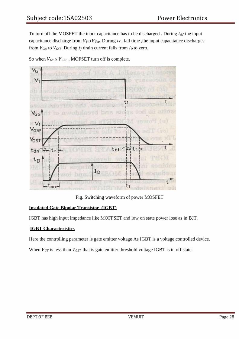
To turn off the MOSFET the input capacitance has to be discharged . During 𝑡𝑑𝑓 the input
capacitance discharge from 𝑉1to 𝑉𝐺𝑠𝑝. During 𝑡𝑓 , fall time ,the input capacitance discharges
from 𝑉𝐺𝑠𝑝 to 𝑉𝐺𝑆𝑇. During 𝑡𝑓 drain current falls from 𝐼𝐷 to zero.
So when 𝑉𝐺𝑠 ≤ 𝑉𝐺𝑆𝑇 , MOFSET turn off is complete.
Fig. Switching waveform of power MOSFET
Insulated Gate Bipolar Transistor (IGBT)
IGBT has high input impedance like MOFFSET and low on state power lose as in BJT.
IGBT Characteristics
Here the controlling parameter is gate emitter voltage As IGBT is a voltage controlled device.
When 𝑉𝐺𝐸 is less than 𝑉𝐺𝐸𝑇 that is gate emitter threshold voltage IGBT is in off state.
Subject code:15A02503 Power Electronics
DEPT.OF EEE VEMUIT Page 29
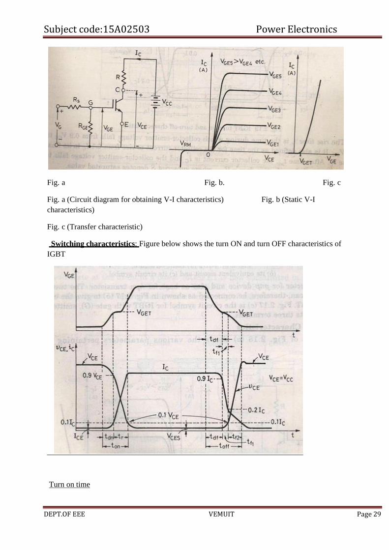
Fig. a Fig. b. Fig. c
Fig. a (Circuit diagram for obtaining V-I characteristics) Fig. b (Static V-I
characteristics)
Fig. c (Transfer characteristic)
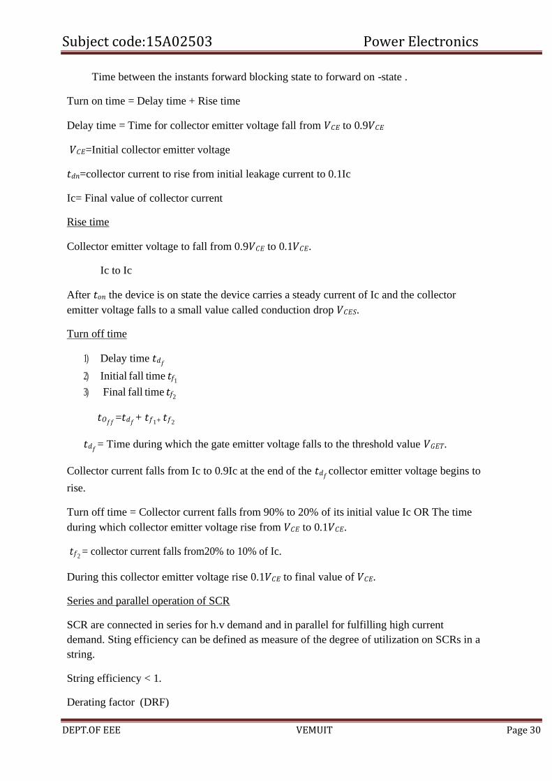
Switching characteristics: Figure below shows the turn ON and turn OFF characteristics of
IGBT
Turn on time
Subject code:15A02503 Power Electronics
DEPT.OF EEE VEMUIT Page 30
Time between the instants forward blocking state to forward on -state .
Turn on time = Delay time + Rise time
Delay time = Time for collector emitter voltage fall from 𝑉𝐶𝐸 to 0.9𝑉𝐶𝐸
𝑉𝐶𝐸=Initial collector emitter voltage
𝑡𝑑𝑛=collector current to rise from initial leakage current to 0.1Ic
Ic= Final value of collector current
Rise time
Collector emitter voltage to fall from 0.9𝑉𝐶𝐸 to 0.1𝑉𝐶𝐸.
Ic to Ic
After 𝑡𝑜𝑛 the device is on state the device carries a steady current of Ic and the collector
emitter voltage falls to a small value called conduction drop 𝑉𝐶𝐸𝑆.
Turn off time
1) Delay time 𝑡𝑑𝑓
2) Initial fall time 𝑡𝑓1
3) Final fall time 𝑡𝑓2
𝑡𝑂𝑓𝑓 =𝑡𝑑𝑓
+ 𝑡𝑓1+ 𝑡𝑓2
𝑡𝑑𝑓 = Time during which the gate emitter voltage falls to the threshold value 𝑉𝐺𝐸𝑇.
Collector current falls from Ic to 0.9Ic at the end of the 𝑡𝑑𝑓 collector emitter voltage begins to
rise.
Turn off time = Collector current falls from 90% to 20% of its initial value Ic OR The time
during which collector emitter voltage rise from 𝑉𝐶𝐸 to 0.1𝑉𝐶𝐸.
𝑡𝑓2 = collector current falls from20% to 10% of Ic.
During this collector emitter voltage rise 0.1𝑉𝐶𝐸 to final value of 𝑉𝐶𝐸.
Series and parallel operation of SCR
SCR are connected in series for h.v demand and in parallel for fulfilling high current
demand. Sting efficiency can be defined as measure of the degree of utilization on SCRs in a
string.
String efficiency < 1.
Derating factor (DRF)
Subject code:15A02503 Power Electronics
DEPT.OF EEE VEMUIT Page 31
1 – string efficiency.
If DRF more then
no. of SCRs will more, so string is more reliable.
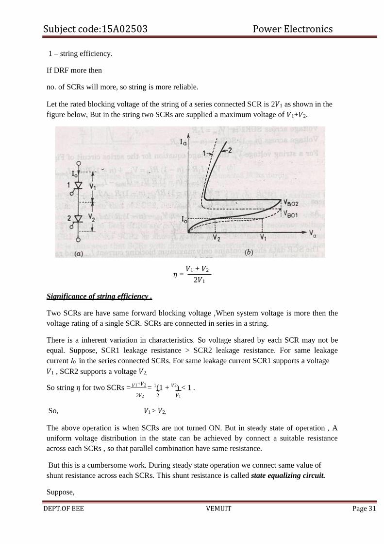
Let the rated blocking voltage of the string of a series connected SCR is 2𝑉1 as shown in the
figure below, But in the string two SCRs are supplied a maximum voltage of 𝑉1+𝑉2.
Significance of string efficiency .
𝜂 = 𝑉1 + 𝑉2
2𝑉1
Two SCRs are have same forward blocking voltage ,When system voltage is more then the
voltage rating of a single SCR. SCRs are connected in series in a string.
There is a inherent variation in characteristics. So voltage shared by each SCR may not be
equal. Suppose, SCR1 leakage resistance > SCR2 leakage resistance. For same leakage
current 𝐼0 in the series connected SCRs. For same leakage current SCR1 supports a voltage
𝑉1 , SCR2 supports a voltage 𝑉2,
So string 𝜂 for two SCRs = 𝑉1+𝑉2 = 1(1 + 𝑉
2) < 1 .
2𝑉2 2 𝑉1
So, 𝑉1 > 𝑉2,
The above operation is when SCRs are not turned ON. But in steady state of operation , A
uniform voltage distribution in the state can be achieved by connect a suitable resistance
across each SCRs , so that parallel combination have same resistance.
But this is a cumbersome work. During steady state operation we connect same value of
shunt resistance across each SCRs. This shunt resistance is called state equalizing circuit.
Suppose,
Subject code:15A02503 Power Electronics
DEPT.OF EEE VEMUIT Page 32
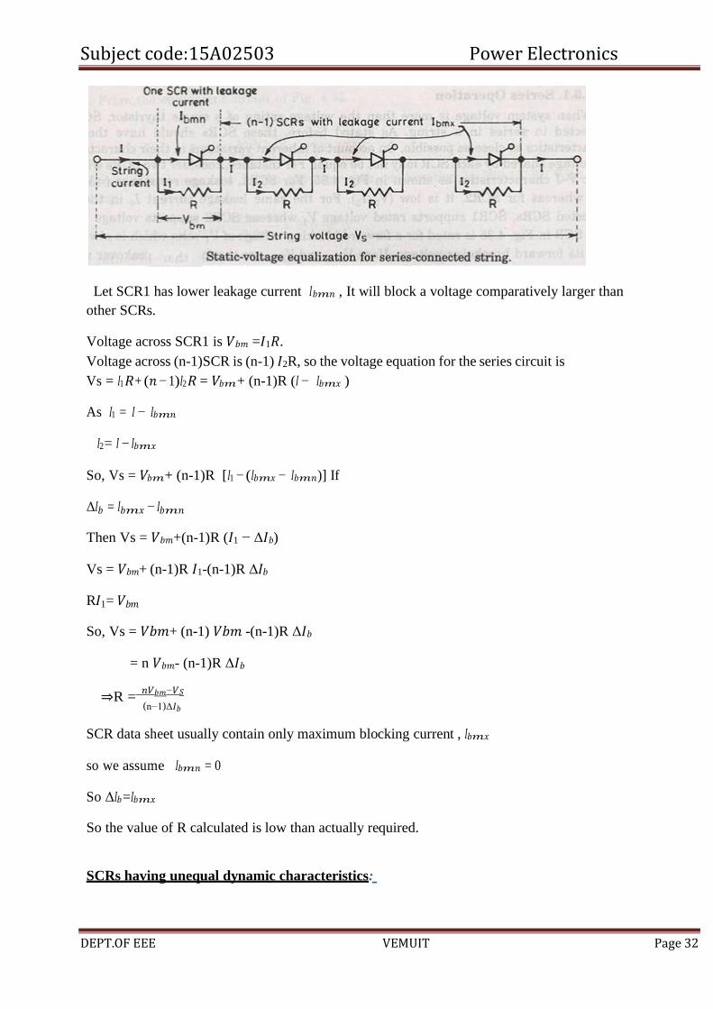
Let SCR1 has lower leakage current 𝐼𝑏𝑚𝑛 , It will block a voltage comparatively larger than
other SCRs.
Voltage across SCR1 is 𝑉𝑏𝑚 =𝐼1𝑅.
Voltage across (n-1)SCR is (n-1) 𝐼2R, so the voltage equation for the series circuit is
Vs = 𝐼1𝑅+ (𝑛 − 1)𝐼2𝑅 = 𝑉𝑏𝑚+ (n-1)R (𝐼 − 𝐼𝑏𝑚𝑥 )
As 𝐼1 = 𝐼 − 𝐼𝑏𝑚𝑛
𝐼2= 𝐼 − 𝐼𝑏𝑚𝑥
So, Vs = 𝑉𝑏𝑚+ (n-1)R [𝐼1 − (𝐼𝑏𝑚𝑥 − 𝐼𝑏𝑚𝑛)] If
Δ𝐼𝑏 = 𝐼𝑏𝑚𝑥 − 𝐼𝑏𝑚𝑛
Then Vs = 𝑉𝑏𝑚+(n-1)R (𝐼1 − Δ𝐼𝑏)
Vs = 𝑉𝑏𝑚+ (n-1)R 𝐼1-(n-1)R Δ𝐼𝑏
R𝐼1= 𝑉𝑏𝑚
So, Vs = 𝑉𝑏𝑚+ (n-1) 𝑉𝑏𝑚 -(n-1)R Δ𝐼𝑏
= n 𝑉𝑏𝑚- (n-1)R Δ𝐼𝑏
⇒R = 𝑛𝑉𝑏𝑚−𝑉𝑆
(n−1)Δ𝐼𝑏
SCR data sheet usually contain only maximum blocking current , 𝐼𝑏𝑚𝑥
so we assume 𝐼𝑏𝑚𝑛 = 0
So Δ𝐼𝑏=𝐼𝑏𝑚𝑥
So the value of R calculated is low than actually required.
SCRs having unequal dynamic characteristics:
Subject code:15A02503 Power Electronics
DEPT.OF EEE VEMUIT Page 33
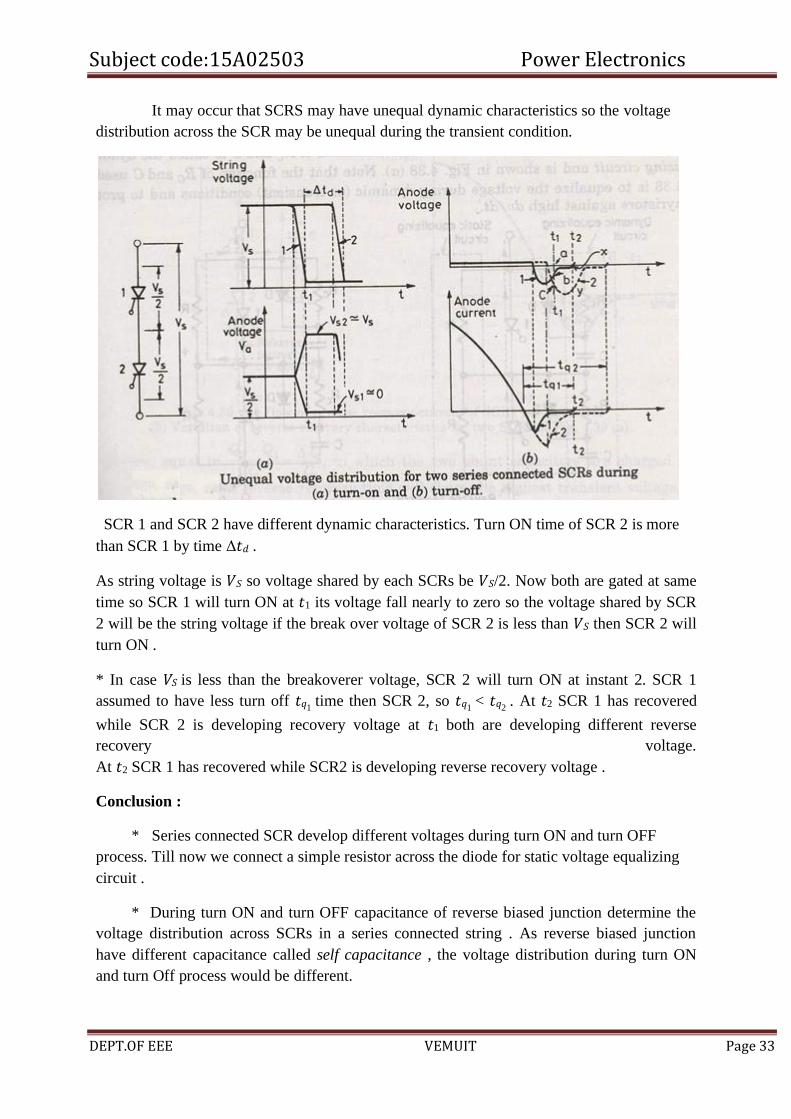
It may occur that SCRS may have unequal dynamic characteristics so the voltage
distribution across the SCR may be unequal during the transient condition.
SCR 1 and SCR 2 have different dynamic characteristics. Turn ON time of SCR 2 is more
than SCR 1 by time Δ𝑡𝑑 .
As string voltage is 𝑉𝑆 so voltage shared by each SCRs be 𝑉𝑆/2. Now both are gated at same
time so SCR 1 will turn ON at 𝑡1 its voltage fall nearly to zero so the voltage shared by SCR
2 will be the string voltage if the break over voltage of SCR 2 is less than 𝑉𝑆 then SCR 2 will
turn ON .
* In case 𝑉𝑆 is less than the breakoverer voltage, SCR 2 will turn ON at instant 2. SCR 1
assumed to have less turn off 𝑡𝑞1 time then SCR 2, so 𝑡𝑞1
< 𝑡𝑞2 . At 𝑡2 SCR 1 has recovered
while SCR 2 is developing recovery voltage at 𝑡1 both are developing different reverse
recovery voltage.
At 𝑡2 SCR 1 has recovered while SCR2 is developing reverse recovery voltage .
Conclusion :
* Series connected SCR develop different voltages during turn ON and turn OFF
process. Till now we connect a simple resistor across the diode for static voltage equalizing
circuit .
* During turn ON and turn OFF capacitance of reverse biased junction determine the
voltage distribution across SCRs in a series connected string . As reverse biased junction
have different capacitance called self capacitance , the voltage distribution during turn ON
and turn Off process would be different.
Subject code:15A02503 Power Electronics
DEPT.OF EEE VEMUIT Page 34
* Under transient condition equal voltage distribution can be achieved by employing
shunt capacitance as this shunt capacitance has the effect of that the resultant of shunt and
self capacitance tend to be equal. The capacitor is used to limits the dv/dt across the SCR
during forward blocking state. When this SCR turned ON capacitor discharges heavy current
through the SCR . The discharge current spike is limited by damping resistor 𝑅𝑐 . 𝑅𝑐 also
damps out high frequency oscilation that may arise due to series combination of 𝑅𝑐 ,C and
series inductor . 𝑅𝑐 & C are called dynamic equalizing circuit
Diode D is used during forward biased condition for more effective charging of the capacitor.
During capacitor discharge 𝑅𝑐 comes into action for limiting current spike and rate of change
of current di/dt .
The R, 𝑅𝑐 & C component also provide path to flow reverse recovery current. When one SCR
regain its voltage blocking capability. The flow of reverse recovery current is necessary as it
facilitates the turning OFF process of series connected SCR string. So C is necessary for both
during turn ON and turn OFF process. But the voltage unbalance during turn OFF time is
more predominant then turn ON time. So choice of C is based on reverse recovery
characteristic of SCR .
Subject code:15A02503 Power Electronics
DEPT.OF EEE VEMUIT Page 35
2
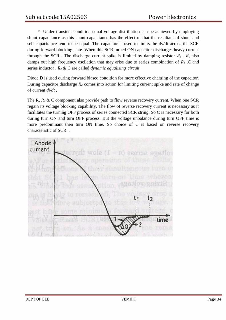
SCR 1 has short recovery time as compared to SCR 2. Δ𝑄 is the difference in reverse
recovery charges of two SCR 1 and SCR 2. Now we assume the SCR 1 recovers fast . i.e it
goes into blocking state so charge Δ𝑄 can pass through C . The voltage induced by 𝑐1 is
𝛥𝑄/C , where is no voltage induced across 𝐶2 .
The difference in voltage to which the two shunt capacitor are charged is 𝛥𝑄/C .
Now thyristor with least recovery time will share the highest transient
voltage say 𝑉𝑏𝑚,
So, 𝑉𝑏𝑚 - 𝑉2 = Δ𝑄/C
So, 𝑉2= 𝑉𝑏𝑚 - Δ𝑄/C
As 𝑉1 = 𝑉𝑏𝑚
𝑉𝑆 = 𝑉1+𝑉2
= 𝑉𝑏𝑚+(𝑉𝑏𝑚 - Δ𝑄/C)
𝑉𝑆 = 2𝑉𝑏𝑚-Δ𝑄/C
⇒ 1 (𝑉 + Δ
𝑄) = 𝑉
2 𝑠 𝐶 𝑏𝑚
⇒ 𝑉2= 𝑉𝑏𝑚 - Δ𝑄/C
1[𝑉𝑠 - Δ𝑄/C]
Now suppose that there are n series SCRs in a string.
Subject code:15A02503 Power Electronics
DEPT.OF EEE VEMUIT Page 36
𝑛
Let us assume that if top SCR has similar to characteristic SCR 1. Then SCR 1 would
support a voltage 𝑉𝑏𝑚
* If the remaining (n-1) SCR has characteristic that of SCR 2 .Then SCR 1
would recover first and support a voltage 𝑉𝑏𝑚 . The charge (n-1) Δ𝑄 from the remaining (n -
1) SCR would pass through C.
𝑉1 = 𝑉𝑏𝑚
𝑉2 = 𝑉𝑏𝑚 - Δ𝑄/C
Voltage across (n-1) slow thyristors
𝑉 = (n-1) (𝑉𝑏𝑚 - Δ𝑄/C)
So, 𝑉𝑆 = V1+(n-1) 𝑉2
= 𝑉𝑏𝑚 + (n-1) (𝑉𝑏𝑚 - Δ𝑄/C)
By simplifing we get ,
Parallel operation:
𝑉𝑏𝑚 = 1 [𝑉𝑠+(n-1) Δ𝑄/C ]
C =[ (n-1) Δ𝑄/( n𝑉𝑏𝑚 -𝑉𝑆)
𝑉2 = (𝑉𝑆 - Δ𝑄/C )/ n .
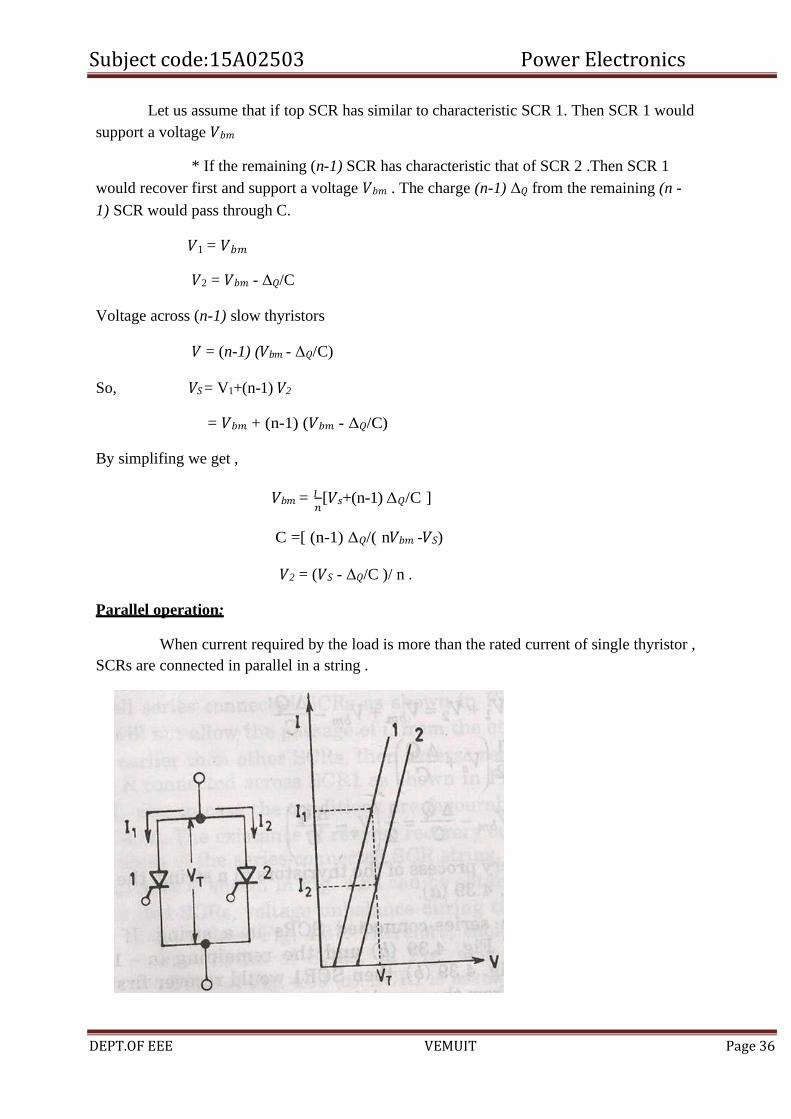
When current required by the load is more than the rated current of single thyristor ,
SCRs are connected in parallel in a string .
Subject code:15A02503 Power Electronics
DEPT.OF EEE VEMUIT Page 37
For equal sharing of current, SCRs must have same 𝑉 − 𝐼characteristics during forward
conduction. 𝑉𝑇 across them must be same. For same 𝑉𝑇 , SCR 1 share 𝐼1and SCR 2 share I2 .
If 𝐼1 is the rated current
𝐼2 < 𝐼1
The total current 𝐼1+𝐼2 and not rated current 2𝐼1.Type equation here.
Thus string efficiency ,
𝐼1+𝐼𝐼2 =
1 (1 +
𝐼𝐼2)
2𝐼1 2 𝐼1
Middle conductor will have more inductance as compared to other two nearby conductor. As
a result less current flow through the middle conductor. Another method is by magnetic
coupling.
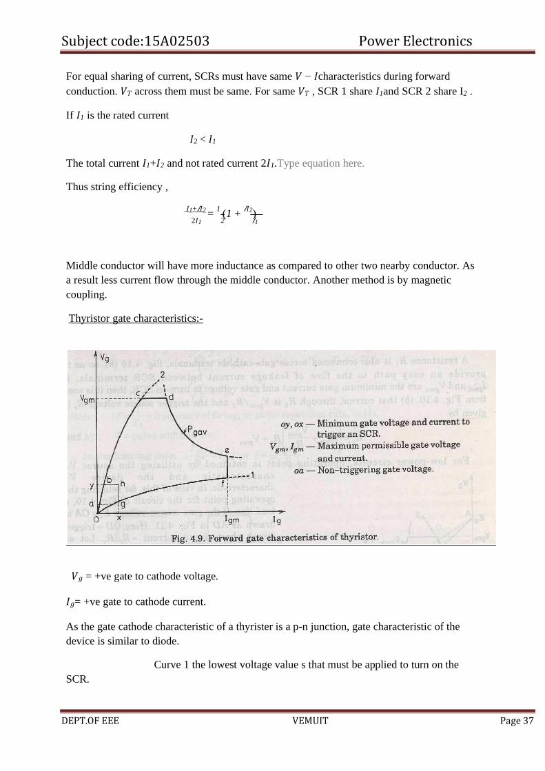
Thyristor gate characteristics:-
𝑉𝑔 = +ve gate to cathode voltage.
𝐼𝑔= +ve gate to cathode current.
As the gate cathode characteristic of a thyrister is a p-n junction, gate characteristic of the
device is similar to diode.
Curve 1 the lowest voltage value s that must be applied to turn on the
SCR.
Subject code:15A02503 Power Electronics
DEPT.OF EEE VEMUIT Page 38
Curve 2 highest possible voltage values that can be safely applied to get circuit.
𝑉gm= Maximum limit for gate voltage .
𝐼gm= Maximum imilt for gate current.
𝑃gav = Rated gate power dissipation for each SCR.
These limits should not be crossed in order to avoid the permanent damage of the
device junction 𝐽3.
OY = Minimum limit of gate voltage to turn ON .
OX = minimum limit of gate current to turn ON.
If 𝑉gm, 𝐼gm, 𝑃gav are exceeded the thyristor will damage so the preferred gate drive area of
SCR is bcdefghb.
oa = The non triggering gate voltage , If firing circuit generates +ve gate
signal prior to the desired instant of triggering the SCR.It should be ensured that this un
wanted signal should be less than the non –triggering voltage oa.
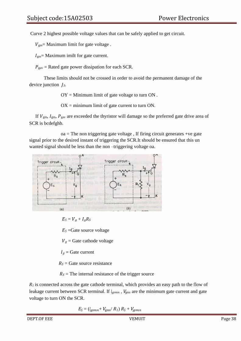
𝐸𝑆 = 𝑉𝑔 + 𝐼𝑔𝑅𝑆
𝐸𝑆 =Gate source voltage
𝑉𝑔 = Gate cathode voltage
𝐼𝑔 = Gate current
𝑅𝑆 = Gate source resistance
𝑅𝑆 = The internal resistance of the trigger source
𝑅1 is connected across the gate cathode terminal, which provides an easy path to the flow of
leakage current between SCR terminal. If 𝐼𝑔𝑚𝑛 , 𝑉gmn are the minimum gate current and gate
voltage to turn ON the SCR.
𝐸𝑆 = (𝐼𝑔𝑚𝑛+ 𝑉gmn/ 𝑅1) 𝑅𝑆 + 𝑉𝑔𝑚𝑛
Subject code:15A02503 Power Electronics
DEPT.OF EEE VEMUIT Page 39
UNIT-II
PHASE CONTROLLED CONVERTERS

Subject code:15A02503 Power Electronics
DEPT.OF EEE VEMUIT Page 40
RECTIFIER
Rectifier are used to convert A.C to D.C supply.
Rectifiers can be classified as single phase rectifier and three phase rectifier. Single phase
rectifier are classified as 1-Փ half wave and 1-Փ full wave rectifier. Three phase rectifier are
classified as 3-Փ half wave rectifier and 3-Փ full wave rectifier. 1-Փ Full wave rectifier are
classified as1-Փ mid point type and 1-Փ bridge type rectifier. 1-Փ bridge type rectifier are
classified as 1-Փ half controlled and 1-Փ full controlled rectifier. 3-Փ full wave rectifier are
again classified as 3-Փ mid point type and 3-Փ bridge type rectifier. 3-Փ bridge type rectifier
are again divided as 3-Փ half controlled rectifier and 3-Փ full controlled rectifier.
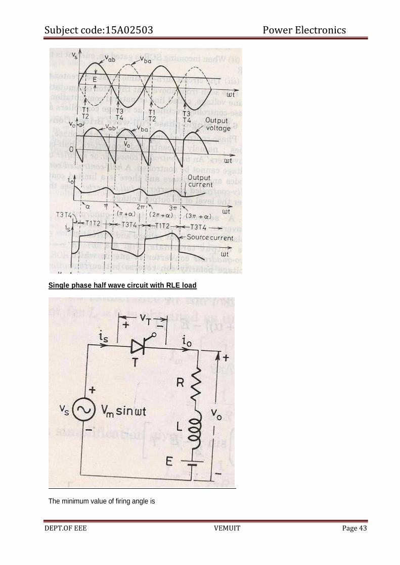
Single phase half wave circuit with R-L load
Output current 𝑖𝑜 rises gradually. After some time 𝑖𝑜 reaches a maximum value and then
begins to decrease.
At π, 𝑣𝑜=0 but 𝑖𝑜 is not zero because of the load inductance L. After π interval SCR is reverse
biased but load current is not less then the holding current.
At β>π, 𝑖𝑜 reduces to zero and SCR is turned off.
At 2π+β SCR triggers again
α is the firing angle.
Subject code:15A02503 Power Electronics
DEPT.OF EEE VEMUIT Page 41
R2 + X
2
Vm
β is the extinction angle.
v = − = conduction angle
Analysis for 𝑉𝑇.
At 𝜔𝑡 = 𝐼,𝑉𝑇 = 𝑉𝑚𝑠𝑖𝑛𝐼
During = 𝐼 𝑡𝑜 𝐼 , 𝑉𝑇 = 0;
When = 𝐼 , 𝑉𝑇 = 𝑉𝑚𝑠𝑖𝑛𝐼;
Vm sin t = Ri0 L di0
dt
is = sin( t−)
Where,
= tan−1 X
R
X = L
Where 𝐼 is the angle by which 𝐼𝑠 lags 𝑉𝑠.
The transient component can be obtained as
Rit + L
di0 = 0 dt
So 𝑖𝑡 = 𝐴𝑒−(𝑅𝑡⁄𝐿)
𝑖0 = 𝑖𝑠 + 𝑖𝑡
𝑉𝑚 sin( 𝜔𝑡 − 𝐼) + 𝐴𝑒−(𝑅𝑡⁄𝐿)
𝑧
Where 𝑧 = √𝑅2 + 𝑋2
At 𝛼 = 𝜔𝑡, 𝑖𝑜 = 0;
0 = 𝑉𝑚
sin( 𝛼 − 𝐼) + 𝐴𝑒−(𝑅𝛼⁄𝐿𝜔); 𝑧
𝐴 = −𝑉𝑚
sin( 𝛼 − 𝐼)𝑒(𝑅𝛼⁄𝐿𝜔)
𝑧
𝑖 = 𝑉𝑚
sin( 𝜔𝑡 − 𝐼) − 𝑉𝑚
sin( 𝛼 − 𝐼)𝑒−𝑅(𝜔𝑡−𝛼)⁄𝐿𝜔
𝑜 𝑧 𝑧
Subject code:15A02503 Power Electronics
DEPT.OF EEE VEMUIT Page 42
Therefore,
𝜔𝑡 = 𝛽, 𝑖0 = 0;
So sin(𝛽 − 𝛼) = sin(𝛼 − 𝐼)𝑒−(𝛽−𝛼)/(𝜔𝐿)
β can obtained from the above equation.
The average load voltage can be given by
1
V0 = 2
Vm sin td (t)
𝑉𝑚 (cos(𝛼) − cos(𝛽)) 2𝜋
Average load current
I0 = Vm
2 R (cos − cos )
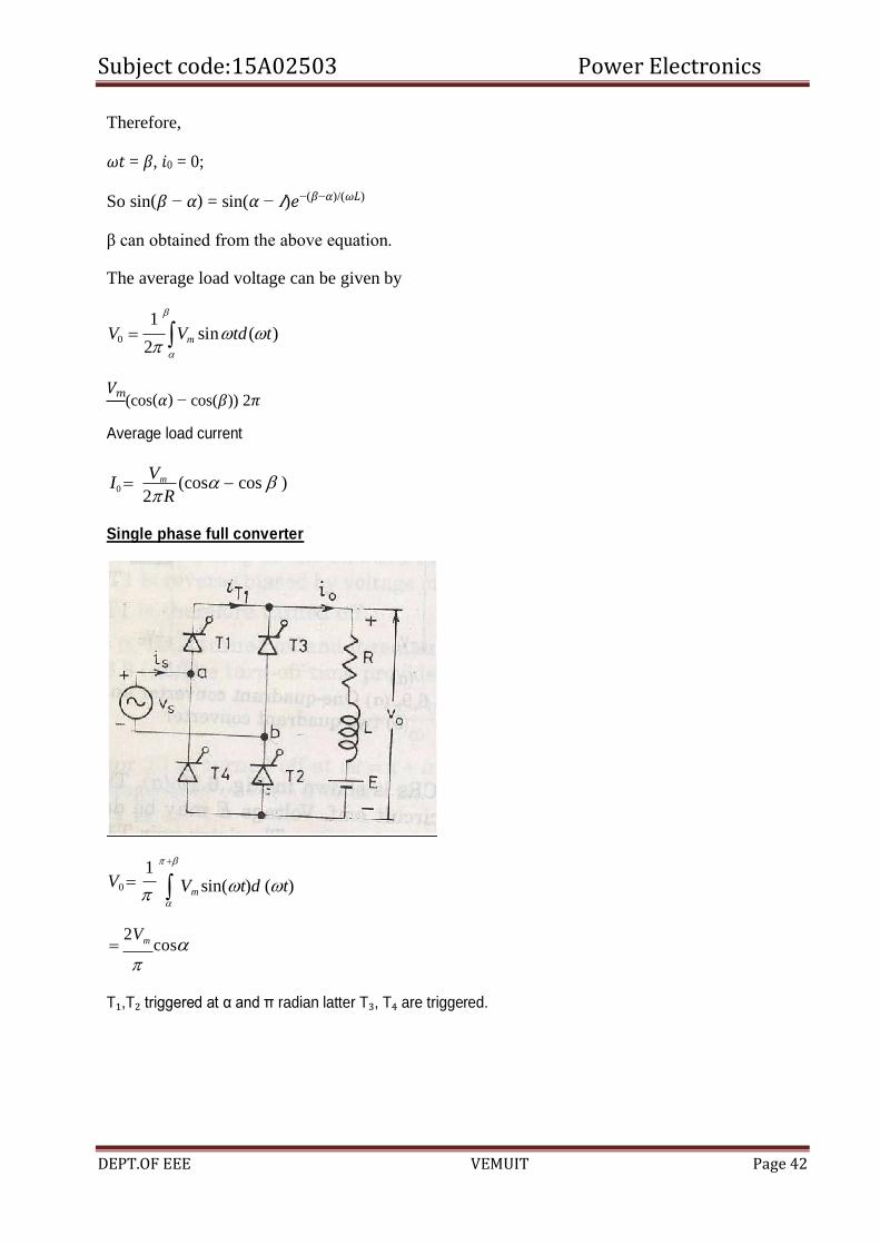
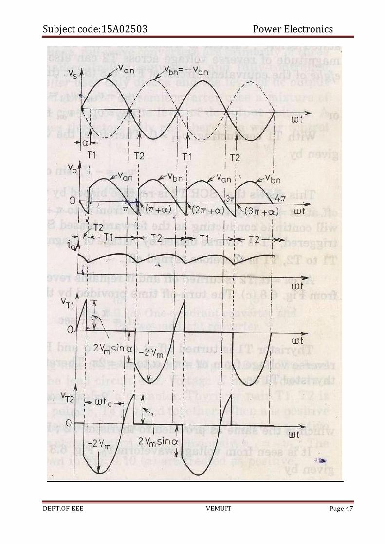
Single phase full converter
1 +
V0 =
Vm sin(t)d (t)
= 2Vm cos
T₁,T₂ triggered at α and π radian latter T₃, T₄ are triggered.
Subject code:15A02503 Power Electronics
DEPT.OF EEE VEMUIT Page 43
Single phase half wave circuit with RLE load
The minimum value of firing angle is
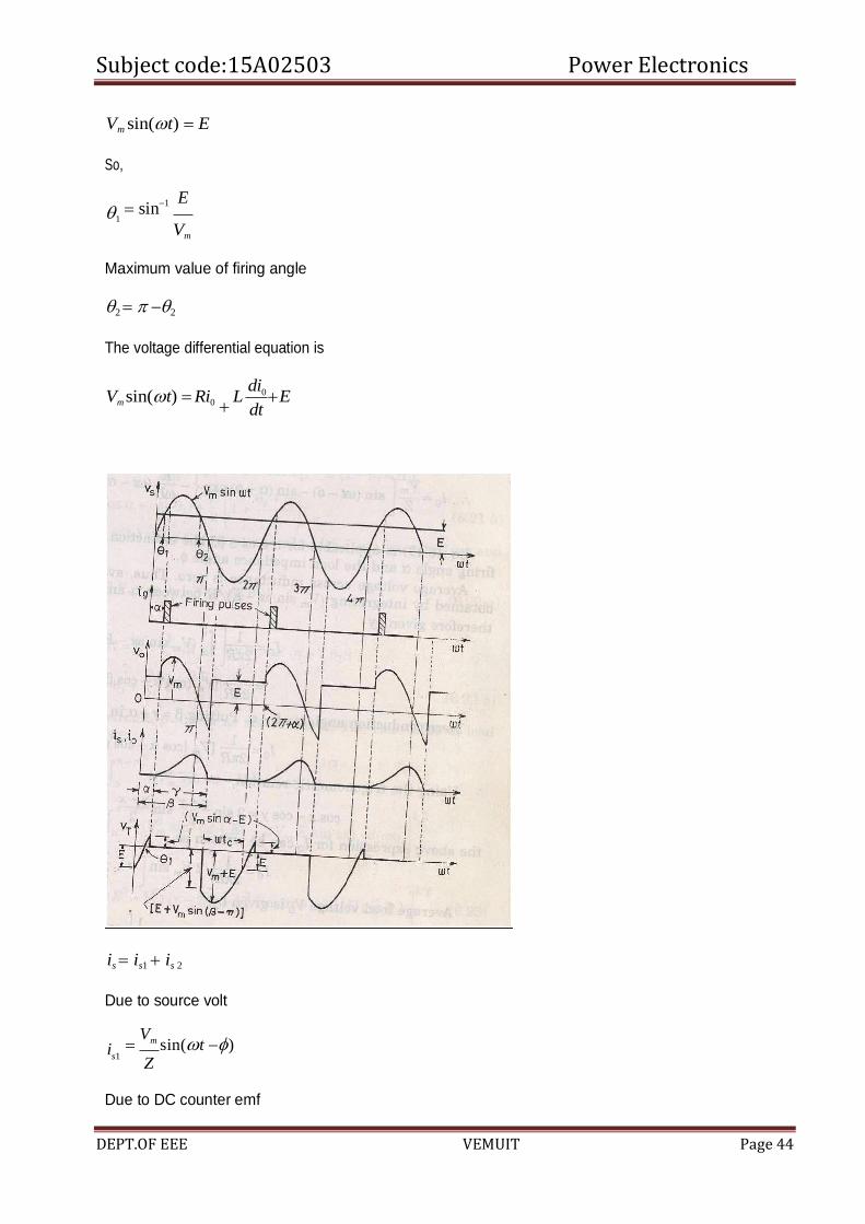
Subject code:15A02503 Power Electronics
DEPT.OF EEE VEMUIT Page 44
Vm sin(t) = E
So,
1
= sin
−1 E
Vm
Maximum value of firing angle
2 = −2
The voltage differential equation is
Vm sin(t) = Ri0 +
L di0 + E dt
is = is1 + is 2
Due to source volt
is1
= Vm sin(t −) Z
Due to DC counter emf
Subject code:15A02503 Power Electronics
DEPT.OF EEE VEMUIT Page 45
t
is 2 = −(E / R)
i = Ae−( R/ L)t
Thus the total current is given by
is1 + is 2 + it
= Vm sin(t −) −
E + Ae
−(R/L) t
Z R
is0
= Vm sin(t −) −
E + Ae
−(R/L) t
Z R
At t = i0 = 0
A = [ E
− V
m sin( −)]e− R L
R Z
So
V { − R
(t − )} E =
{
− R (t − )
i m [sin(t −) − sin( −)e L − [1− e L ] 0
Z R
Average voltage across the inductance is zero. Average value of load current is
I = 1
(V sin t − E) d(t)
0 2 R m
= 1
[V
(cos − cos ) − ( − )]
2 R m
Conduction angle = −
= + v
I0 = 1
2 R [Vm (cos − cos( + v)) − (v)]
cos A − cosB = 2sin A + B
sin A − B
2 2
So
I0 =
1
2 R
[2Vm
sin( + v
) sin v
− E. ] 2 2

Subject code:15A02503 Power Electronics
DEPT.OF EEE VEMUIT Page 46
) sin ]
= E + I0 R
= E+ 1
2 [2Vm sin( +
v ) sin
v − E.
] 2 2
= E(1− v
) + [Vm sin( +
v v
2 2 2
If load inductance L is zero then
= 2
And
v = − = 2 −
But 2 = −1
So = 2 = −1
And v = −1 −
So average current will be
I0 = 1
2 R [Vm (cos − cos( −1 )) − E( −1 − )]
So V0=E+I0R
= Vm (cos + cos ) +
E (1+
1 + )
2 1
2
For no inductance rms value of load current
I = [ 1 −
2 1/2
0 2 R2
(Vm sin( t) − E) d (t )]
Power delivered to load
P = I
2 R + I E
or 0
Supply power factor
I
2 R + I E
Pf = or 0
Vs Ior
Single phase full wave converter:
Subject code:15A02503 Power Electronics
DEPT.OF EEE VEMUIT Page 47
Subject code:15A02503 Power Electronics
DEPT.OF EEE VEMUIT Page 48
V = 1 +
V
sin(t)d (t)
0 m
= 2Vm sin
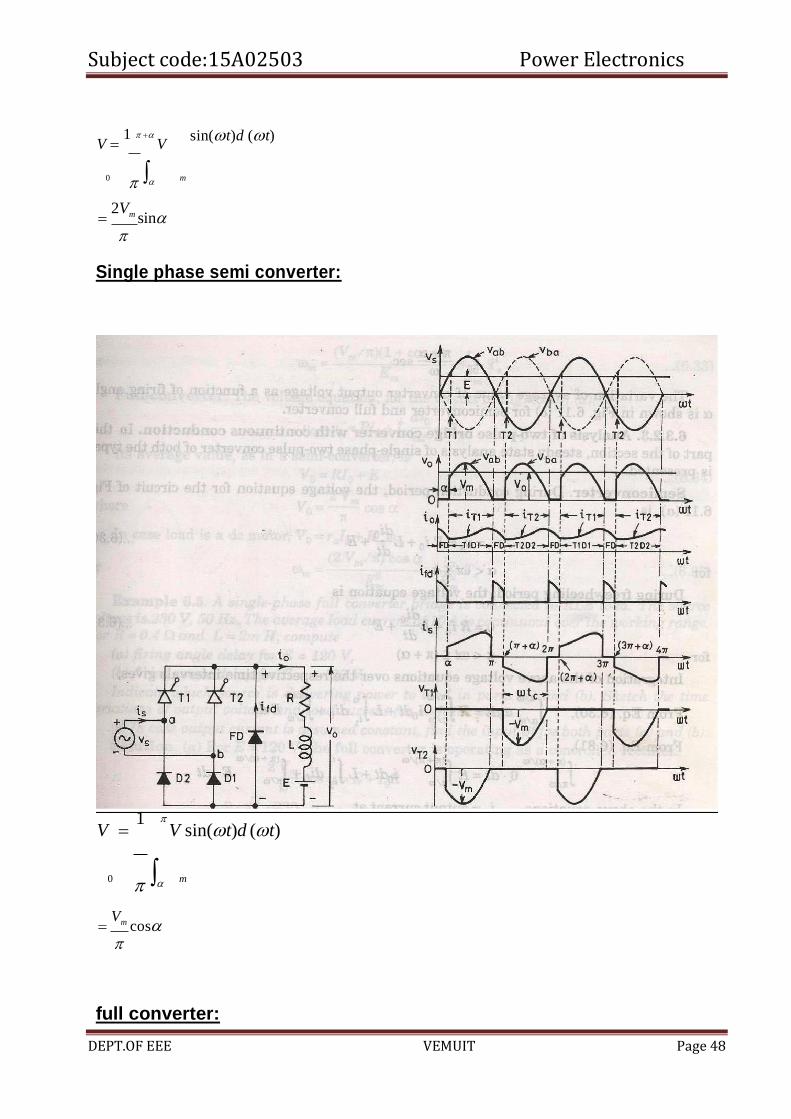
Single phase semi converter:
V = 1
V sin(t)d (t)
0 m
= Vm cos
full converter:

Subject code:15A02503 Power Electronics
DEPT.OF EEE VEMUIT Page 49
2
m
steady state analysis
V = Ri + L di0 + E
s o dt
V0 = RI0 + E
V = 2Vm cos
0
So in case of DC motor load
V0 = ra Ia +mm
2Vm cos − r I
a a
m =
So m
T = m Ia
Ia = Te
Put
Ia =
m
Te
m
(
2Vm ) cos
= − raTe
So m m
Subject code:15A02503 Power Electronics
DEPT.OF EEE VEMUIT Page 50
UNIT-III
CHOPPERS AND REGULATORS
Subject code:15A02503 Power Electronics
DEPT.OF EEE VEMUIT Page 51
0
1
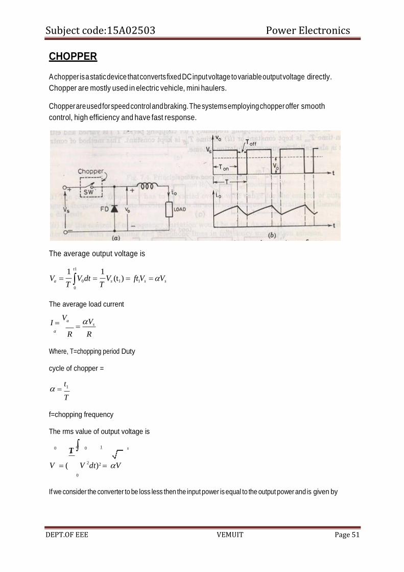
CHOPPER
A chopper is a static device that converts fixed DC input voltage to variable output voltage directly.
Chopper are mostly used in electric vehicle, mini haulers.
Chopper are used for speed control and braking. The systems employing chopper offer smooth
control, high efficiency and have fast response.
The average output voltage is
1 t1
1
Va = T
V0dt = T
Vs (t1 ) = ft1Vs = Vs
The average load current
I = Va
=
Vs
a R R
Where, T=chopping period Duty
cycle of chopper =
= t1
T
f=chopping frequency The rms value of output voltage is
1 0 T 0 s
V = ( V 2dt)2 = V
0
If we consider the converter to be loss less then the input power is equal to the output power and is given by
Subject code:15A02503 Power Electronics
DEPT.OF EEE VEMUIT Page 52
o
I a
1 T
1 T
V 2
Pi = T
V0idt = T R
dt 0 0
1 V 2 V 2
= s (T ) = s
T R R
The effective input resistance seen by the P source is
P = Vs =
Vs = R
i Vs
R
The duty cycle α can be varied by varying t₁ , T of frequency.
Constant frequency operation:
1) The chopping period T is kept constant and on time is varied. The
pulse width modulation ,the width of the pulse is varied.
2) Variable frequency operation, the chopping frequency f is varied.
Frequency modulation, either on time or off time is kept constant.
This type of control generate harmonics at unpredictable frequency and filter design is often difficult.
TYPES OF CHOPPER:
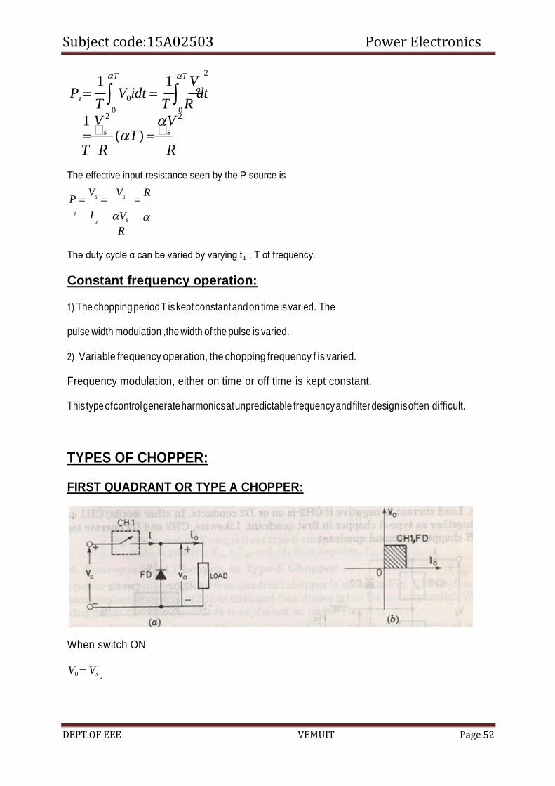
FIRST QUADRANT OR TYPE A CHOPPER:
When switch ON
V0 = Vs .
Subject code:15A02503 Power Electronics
DEPT.OF EEE VEMUIT Page 53
Current i₀ flows in the same direction when switch off. V₀=0,
i₀=0
So, average value of both the load and the current are positive.
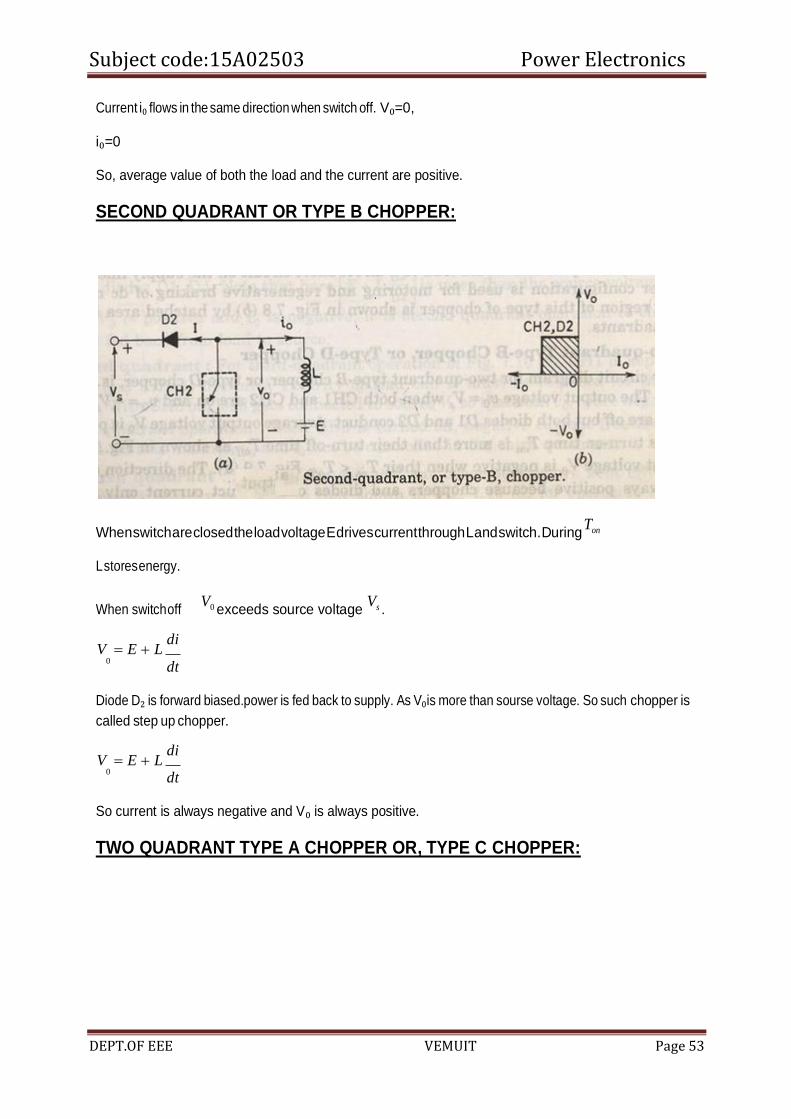
SECOND QUADRANT OR TYPE B CHOPPER:
When switch are closed the load voltage E drives current through L and switch. During Ton
L stores energy.
When switch off
V0 exceeds source voltage
Vs .
V = E + L di
0
dt
Diode D₂ is forward biased.power is fed back to supply. As V₀is more than sourse voltage. So such chopper is
called step up chopper.
V = E + L di
0
dt
So current is always negative and V₀ is always positive.
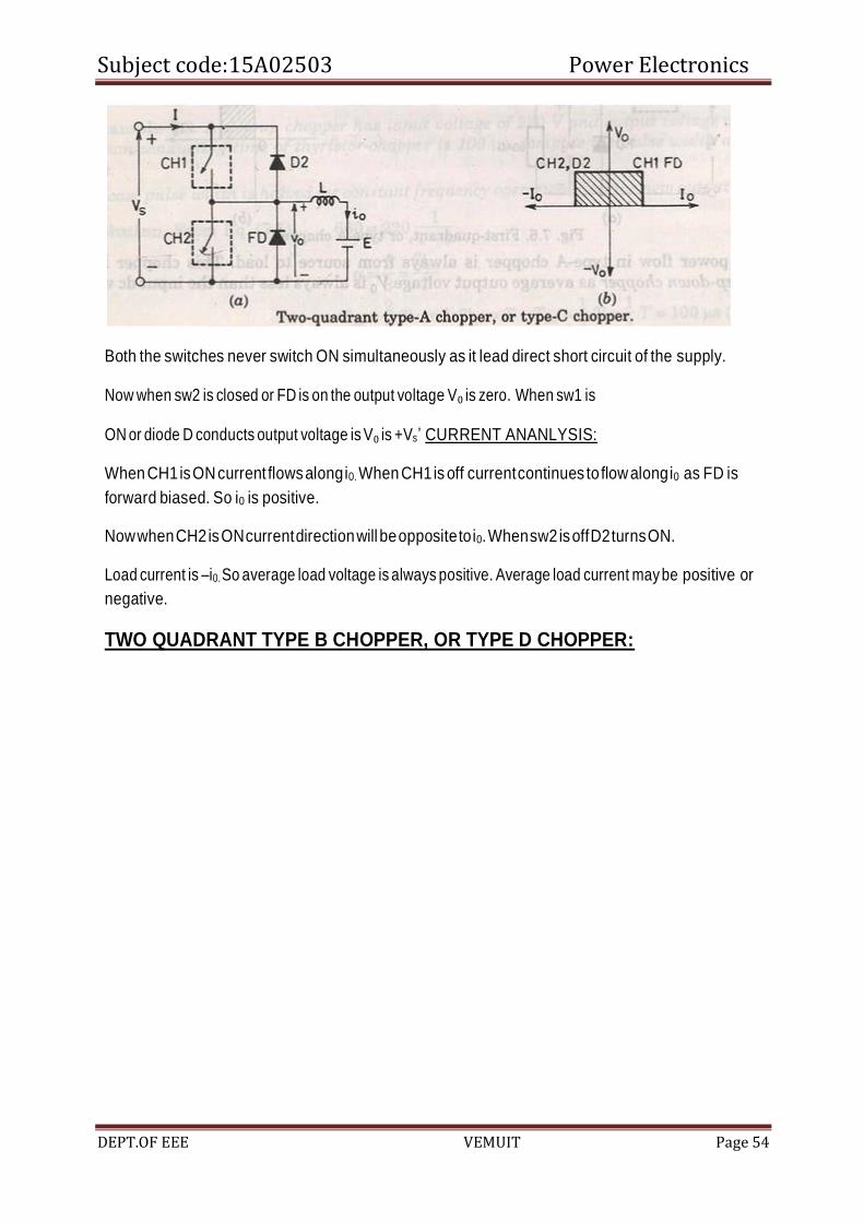
TWO QUADRANT TYPE A CHOPPER OR, TYPE C CHOPPER:
Subject code:15A02503 Power Electronics
DEPT.OF EEE VEMUIT Page 54
Both the switches never switch ON simultaneously as it lead direct short circuit of the supply.
Now when sw2 is closed or FD is on the output voltage V₀ is zero. When sw1 is
ON or diode D conducts output voltage is V₀ is +Vs’ CURRENT ANANLYSIS:
When CH1 is ON current flows along i0. When CH1 is off current continues to flow along i0 as FD is
forward biased. So i0 is positive.
Now when CH2 is ON current direction will be opposite to i0. When sw2 is off D2 turns ON.
Load current is –i0. So average load voltage is always positive. Average load current may be positive or
negative.
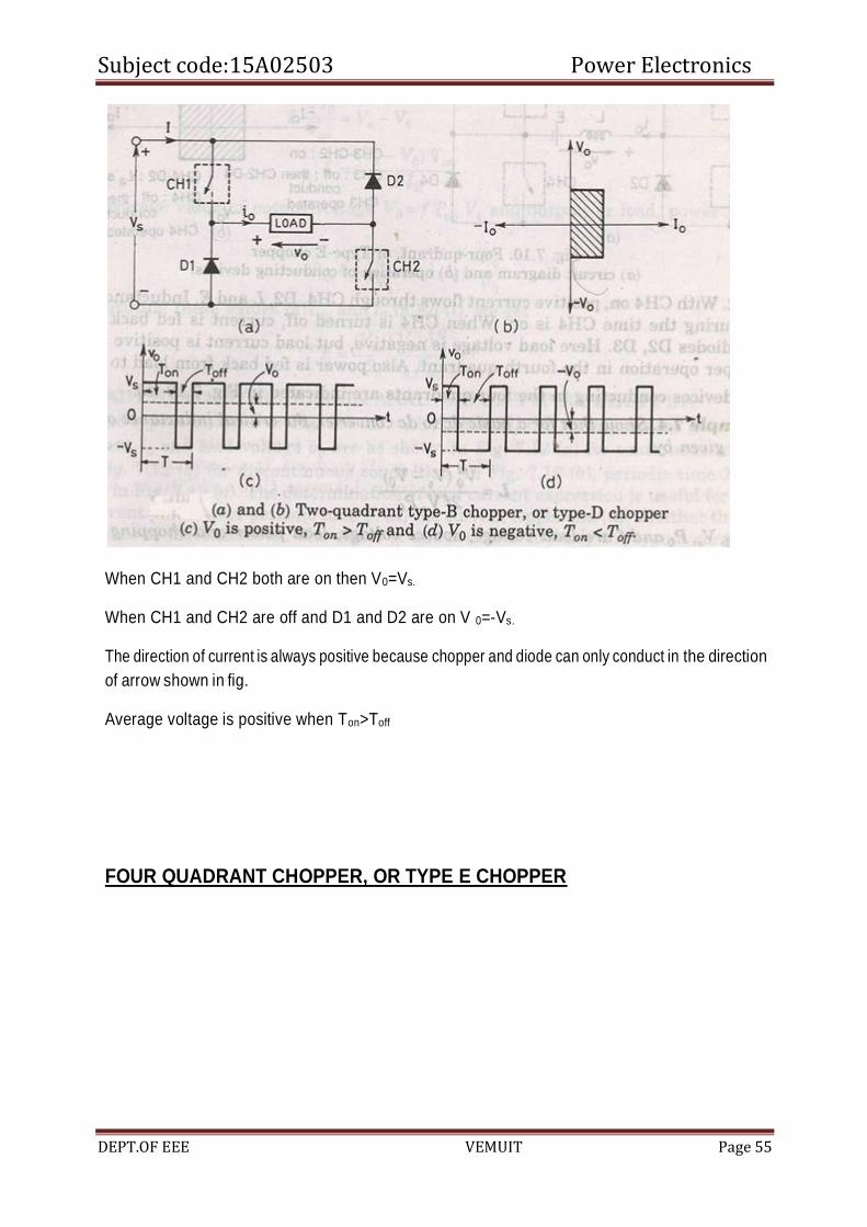
TWO QUADRANT TYPE B CHOPPER, OR TYPE D CHOPPER:
Subject code:15A02503 Power Electronics
DEPT.OF EEE VEMUIT Page 55
When CH1 and CH2 both are on then V0=Vs.
When CH1 and CH2 are off and D1 and D2 are on V 0=-Vs.
The direction of current is always positive because chopper and diode can only conduct in the direction
of arrow shown in fig.
Average voltage is positive when Ton>Toff
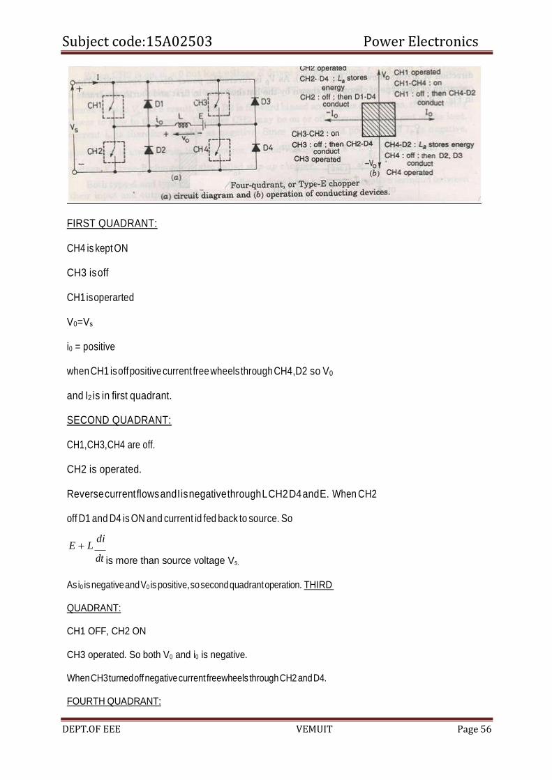
FOUR QUADRANT CHOPPER, OR TYPE E CHOPPER
Subject code:15A02503 Power Electronics
DEPT.OF EEE VEMUIT Page 56
FIRST QUADRANT:
CH4 is kept ON
CH3 is off
CH1 is operarted
V0=Vs
i0 = positive
when CH1 is off positive current free wheels through CH4,D2 so V0
and I2 is in first quadrant.
SECOND QUADRANT:
CH1,CH3,CH4 are off.
CH2 is operated.
Reverse current flows and I is negative through L CH2 D4 and E. When CH2
off D1 and D4 is ON and current id fed back to source. So
E + L di
dt is more than source voltage Vs.
As i0 is negative and V0 is positive, so second quadrant operation. THIRD
QUADRANT:
CH1 OFF, CH2 ON
CH3 operated. So both V0 and i0 is negative.
When CH3 turned off negative current freewheels through CH2 and D4.
FOURTH QUADRANT:

Subject code:15A02503 Power Electronics
DEPT.OF EEE VEMUIT Page 57
2
CH4 is operated other are off.
Positive current flows through CH4 E L D2.
Inductance L stores energy when current fed to source through D3 and D2.V0 is negative.
STEADY STATE ANALYSIS OF PRACTICAL BUCK CHOPPER:
The voltage across the inductor L is e i=Ldi/dt.
V −V = L d (i2 − i1 ) = L
i
t1 t1
t1 = iL
V −V s a .
The inductor current falls linearly from I2 to I1 in time t2 as Vs =0.
So
−Va
=
L(i1 − i2 ) t
2
If I2-I1=ΔI then
−Va = − LI t
2
t = LI
Va .
ΔI=I2-I1= peak to peak ripple current.
I = (Vs −Va ) t1 =
Vat2
L L
Now t1=αT, t2=(1-α)T
V = V t1 = V
a s T
s
Α<1 so it is a step down or buck converter. If the
circuit is lossless then VsIs=Va Ia=αVsIa Is =α Ia.
Now switching period T can be expressed as
s a

Subject code:15A02503 Power Electronics
DEPT.OF EEE VEMUIT Page 58
s
T=1/f= t1+ t2=ΔIL/(Vs-Va) + ΔIL/(Va)
=ΔILVs/Va(Vs-Va)
So peak to peak ripple current
I = Va (Vs −Va )
fLVs
I = Va (1− )
fL
The peak to peak voltage of the capacitor is
Vc =
I
8 fc
So from above equation
V = Va (Vs −Va ) .
Vs (1− )
c 8Lcf
2V 8Lcf
2
Condition for continuous inductor current and capacitor voltage :
If IL is the average inductor current
IL = 2IL ….as
Va = Vs
Vs (1− ) =
fL
I2 − I1 = I
As 2 L
So I = 2IL
Vs (1− )
fL …..eq (2)
Vs (1− ) = 2I
fL L = 2Ia =
2Vs
R
…..eq(4)
Subject code:15A02503 Power Electronics
DEPT.OF EEE VEMUIT Page 59
1
1
As Va = Vs
I = Vs
so a
R
2Ia = 2Vs
R
So equation 4 gives
L = (1− )R
c 2 f
Which is the critical value of inductor
Vc = 2Va
2V = Vs (1− )
= 2V
a 8Lcf
2 s
c = 1−
16Lf 2
Peak to peak ripple voltage of capacitor:
Vc = Vc −Vc (t = 0)
= 1 t1
I dt = 1
t1
I
= Iat1
c 0 c
c 0 a c
t = Va −Vs
So Vaf
t = Va −Vs
Vaf
1− = Vs
Va
1− t1 =
Vs
T Va
t1 = Va −Vs
Va f
Vc
So
= Ia (
Va −Vs )
c Vaf

Subject code:15A02503 Power Electronics
DEPT.OF EEE VEMUIT Page 60
Vc = Ia
fc
Condition for continuous imductor current and capacitor voltage:
If IL= average inductor current then
I = I
L 2
I = Vs
= 2I fL
L = 2Ia = 2Vs
(1− )R
Va = As
Vs
1−
2Ia = 2Vs
(1− ) R
I = 2I = 2I = 2Vs = Vs
So
Lc
L L a
= (1− a)R
2 f
(1− )R fL
Vc = 2Va
Ia = 2V = 2I R
cf a a
c =
2 fR
Subject code:15A02503 Power Electronics
DEPT.OF EEE VEMUIT Page 61
UNIT-IV
INVERTERS
Subject code:15A02503 Power Electronics
DEPT.OF EEE VEMUIT Page 62
⁄
4
01 𝑆
INVERTERS
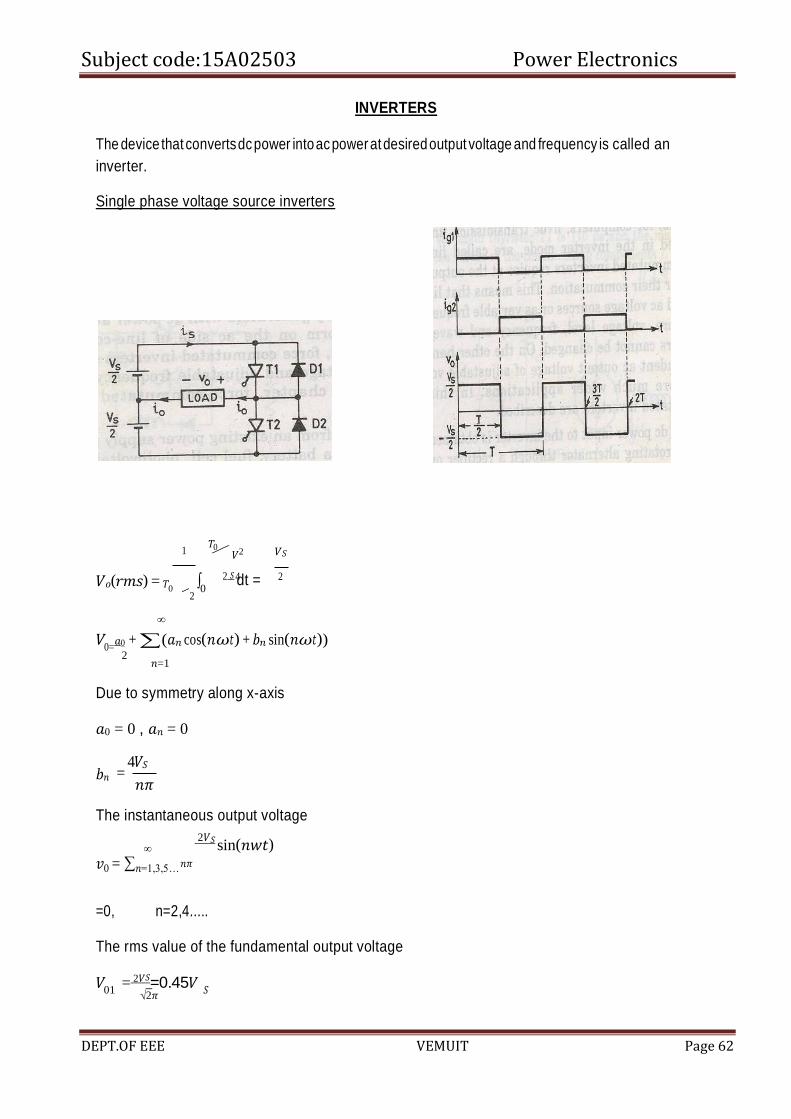
The device that converts dc power into ac power at desired output voltage and frequency is called an
inverter.
Single phase voltage source inverters
1 𝑇0⁄
𝑉2
𝑉𝑆
𝑉𝑜(𝑟𝑚𝑠) = 𝑇0 ∫0
2
2 𝑆 dt =
∞
𝑉0=
𝑎0 + ∑(𝑎𝑛 cos(𝑛𝜔𝑡) + 𝑏𝑛 sin(𝑛𝜔𝑡)) 2
𝑛=1
Due to symmetry along x-axis
𝑎0 = 0 , 𝑎𝑛 = 0
𝑏𝑛 = 4𝑉𝑆
𝑛𝜋
The instantaneous output voltage
∞ 2𝑉𝑆
sin(𝑛𝑤𝑡) 𝑣0 = ∑𝑛=1,3,5… 𝑛𝜋
=0, n=2,4.....
The rms value of the fundamental output voltage
𝑉 = 2𝑉𝑆 =0.45𝑉
√2𝜋
2
Subject code:15A02503 Power Electronics
DEPT.OF EEE VEMUIT Page 63
01 01
1 𝑆
𝑅
So if 𝑉0 = ∑∞ 2𝑉𝑆 sin(𝑛𝑤𝑡)
𝑛=1,3,5… 𝑛𝜋
=∑∞ 2𝑉𝑆 sin(𝑛𝜔𝑡 − 𝜃𝑛)
𝑛=1,3,5…. 𝑛𝜋√𝑅2+(𝑛𝜔𝐿)2
𝑃 = (𝐼 )2𝑅 = [ 2𝑉𝑆
√2𝜋√𝑅2+(𝜔𝐿)2 ]2R
DC Supply Current
Assuming a lossless inverter, the ac power absorbed by the load must be equal to the average
power supplied by the dc source.
∫𝑇 𝑖𝑠(𝑡)𝑑𝑡 = 1 ∫
𝑇 √2𝑉01 sin(𝜔𝑡) √2𝐼0 sin(𝜔𝑡 − 𝜃1) 𝑑𝑡=𝐼𝑆
0 𝑉𝑠 0
𝑉01 =Fundamental rms output output voltage
𝐼0=rms load current
𝜃1=the load angle at the fundamental frequency Single
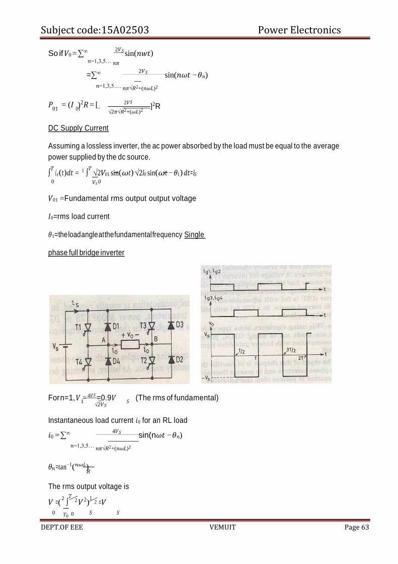
phase full bridge inverter
For n=1, 𝑉 = 4𝑉𝑆 =0.9𝑉 (The rms of fundamental) √2𝑉𝑆
Instantaneous load current 𝑖0 for an RL load
𝑖0 = ∑∞ 4𝑉𝑆 sin(n𝜔𝑡 − 𝜃𝑛) 𝑛=1,3,5… 𝑛𝜋√𝑅2+(𝑛𝜔𝐿)2
𝜃𝑛=tan−1(𝑛𝜔𝐿)
The rms output voltage is 𝑉 =(
2 ∫𝑇⁄2 𝑉2)
1⁄2 =𝑉
0 𝑇0 0 𝑆 𝑆
Subject code:15A02503 Power Electronics
DEPT.OF EEE VEMUIT Page 64
The instantaneous output voltage in a fourier series
𝑣0
∞
= ∑ 4𝑉𝑆
sin(𝑛𝜔𝑡) 𝑛𝜋
𝑛=1,3,5…
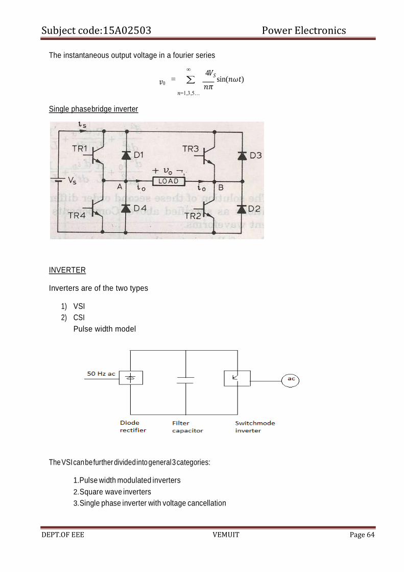
Single phase bridge inverter
INVERTER
Inverters are of the two types
1) VSI
2) CSI
Pulse width model
The VSI can be further divided into general 3 categories:
1.Pulse width modulated inverters
2. Square wave inverters
3. Single phase inverter with voltage cancellation
Subject code:15A02503 Power Electronics
DEPT.OF EEE VEMUIT Page 65
Pulse width modulated inverters
The input dc voltage is of constant magnitude . The diode rectifier is used to rectify the line voltage.The
inverter control the magnitude and frequency of the ac output voltage.
This is achieved by PWM technique of inverter switches and this is called PWM inverters.
The sinusoidal PWM technique is one of the PWM technique to shape the output voltage to as close as
sinusoidal output.
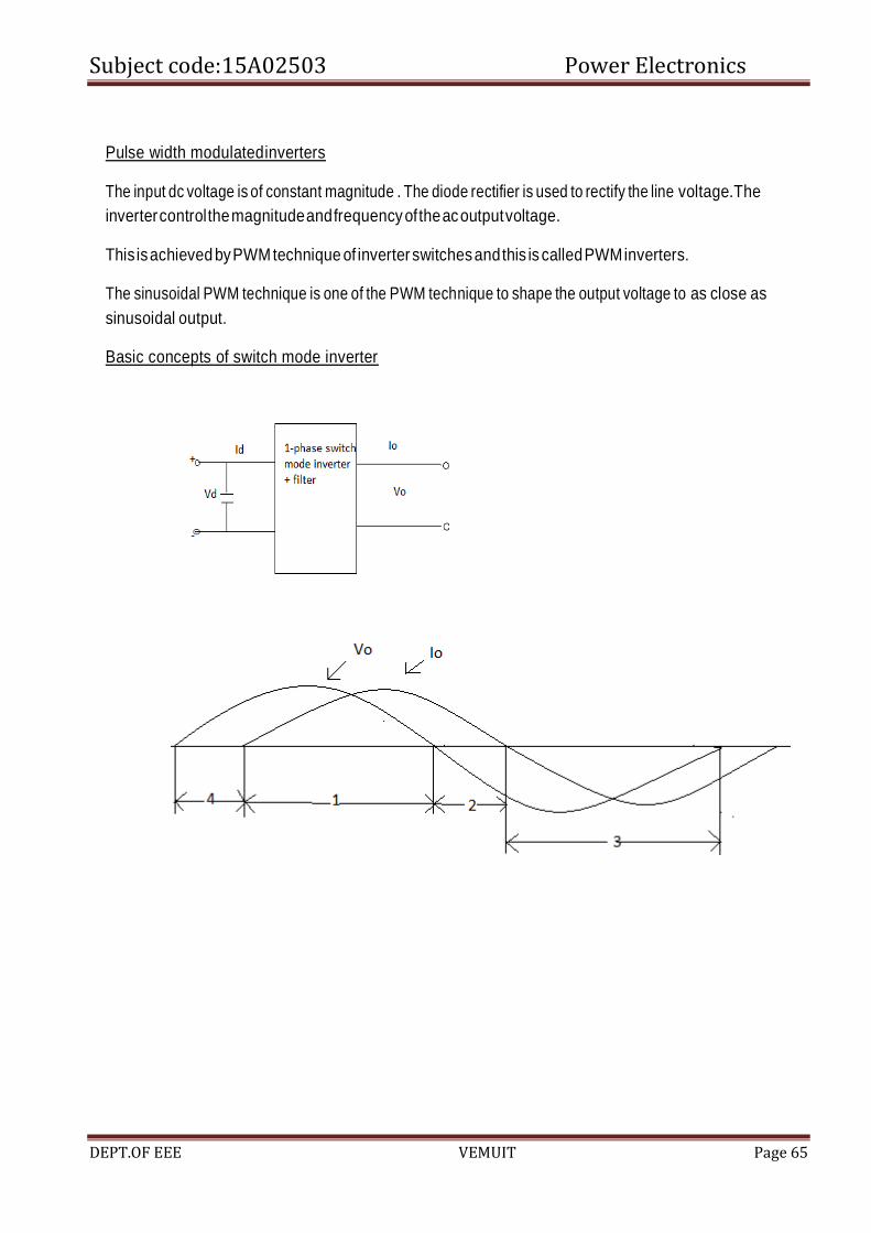
Basic concepts of switch mode inverter

Subject code:15A02503 Power Electronics
DEPT.OF EEE VEMUIT Page 66
During interval 1 𝑣0and 𝑖0 both are positive During
interval 3 𝑣0 and 𝑖0 both are negative
Therefore during 1 and 3 the instantaneous power flow is from dc side to corresponding to inverter
mode of operation.
In contrast during interval 2 and 4 𝑣0 and 𝑖0 are of opposite sign i.e. power flows from ac side to dc
side corresponding to rectifier mode of operation.
Pulse width modulated switching scheme
We require the inverter output to be sinusoidal with magnitude and frequency controllable.
In order to produce sinusoidal output voltage at desired frequency a sinusoidal control signal at
desired frequency is compared with a triangular waveform as show.
The frequency of the triangular waveform established the inverter switching frequency.
The triangular waveform is called carrier waveform. The triangular waveform establishes switching
frequency 𝑓𝑠 , which establishes with which the inverter switches are applied.
The control signal has frequency 𝑓𝑠 and is used to modulate the switch duty ratio.
𝑓1 is the desired fundamental frequency of the output voltage.
The amplitude modulation ratio 𝑚𝑎 is defined as
m 𝑉𝑐𝑜𝑛𝑡𝑟𝑜𝑙
a= 𝑉𝑡𝑟𝑖
Subject code:15A02503 Power Electronics
DEPT.OF EEE VEMUIT Page 67
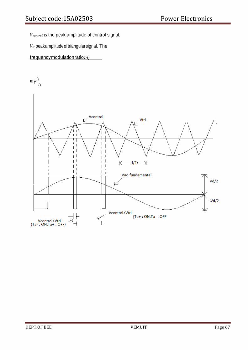
f
𝑉𝑐𝑜𝑛𝑡𝑟𝑜𝑙 is the peak amplitude of control signal.
𝑉𝑡𝑟𝑖 peak amplitude of triangular signal. The
frequency modulation ratio 𝑚𝑓
m = 𝑓𝑠 𝑓1
Subject code:15A02503 Power Electronics
DEPT.OF EEE VEMUIT Page 68
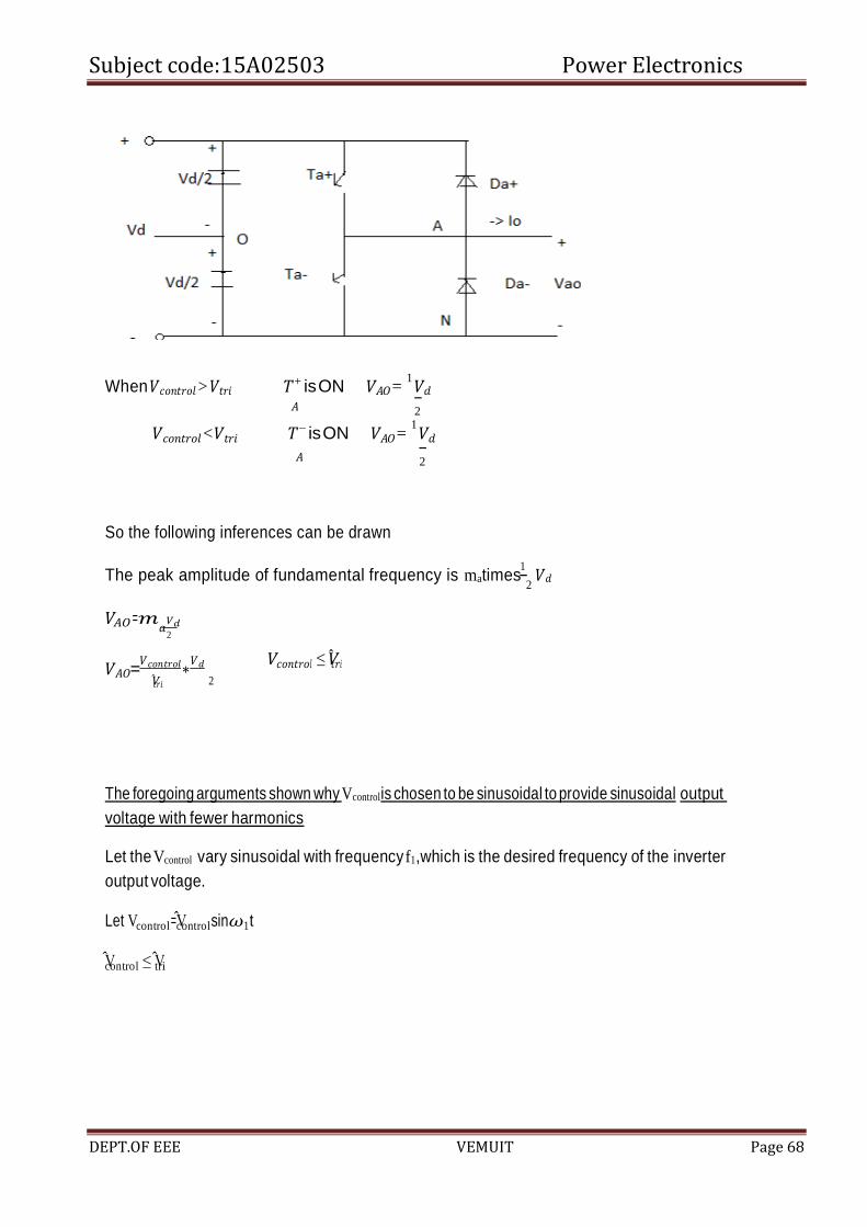
1
2
When 𝑉𝑐𝑜𝑛𝑡𝑟𝑜𝑙 > 𝑉𝑡𝑟𝑖 𝑇+ is ON 𝑉𝐴𝑂 = 1 𝑉𝑑
𝐴 2
𝑉𝑐𝑜𝑛𝑡𝑟𝑜𝑙 < 𝑉𝑡𝑟𝑖 𝑇− is ON 𝑉𝐴𝑂 = 1 𝑉𝑑
𝐴 2
So the following inferences can be drawn
The peak amplitude of fundamental frequency is matimes
2 𝑉𝑑
𝑉𝐴𝑂=𝑚𝑎𝑉𝑑
𝑉𝐴𝑂=𝑉𝑐𝑜𝑛𝑡𝑟𝑜𝑙 ∗
𝑉𝑑 𝑉𝑐𝑜𝑛𝑡𝑟𝑜𝑙 ≤ �̂�𝑡𝑟𝑖 �̂�𝑡𝑟𝑖 2
The foregoing arguments shown why Vcontrolis chosen to be sinusoidal to provide sinusoidal output
voltage with fewer harmonics
Let the Vcontrol vary sinusoidal with frequency f1,which is the desired frequency of the inverter
output voltage.
Let Vcontrol=V̂controlsin𝜔1t
V̂control ≤ V̂tri

Subject code:15A02503 Power Electronics
DEPT.OF EEE VEMUIT Page 69
2
1
�̂�𝑡𝑟𝑖=�̂�𝑡𝑟𝑖
𝑡1 𝑇𝑠⁄4
At t=𝑡1 , 𝑣𝑡𝑟𝑖 =𝑣𝑐𝑜𝑛𝑡𝑟𝑜𝑙
So 𝑣𝑐𝑜𝑛𝑡𝑟𝑜𝑙=
�̂�𝑡𝑟𝑖
𝑡1 𝑇𝑠⁄4
𝑡1=�̂�𝑐𝑜𝑛𝑡𝑟𝑜𝑙*
𝑇𝑆
�̂�𝑡𝑟𝑖 4
𝑇𝑜𝑛=2𝑡1+𝑇𝑆
𝑇 2𝑡1+𝑇𝑆
𝐷1= 𝑜𝑛= 2
𝑇𝑠
=2
+
2
2𝑡1
𝑇𝑠
𝐷 1
1 �̂�𝑐𝑜𝑛𝑡𝑟𝑜𝑙
1=2+
2(
�̂�𝑡𝑟𝑖 )
Three phase inverter
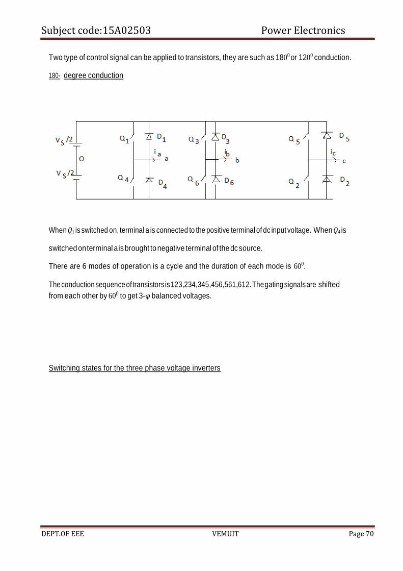
When three single-phase inverters are connected in parallel a three phase inverter is formed.
The gating signal has to be displaced by 1200 with respect to each other so as achieve three phase
balanced voltages.
A 3-phase output can be achieved from a configuration of six transistors and six diodes.
Subject code:15A02503 Power Electronics
DEPT.OF EEE VEMUIT Page 70
Two type of control signal can be applied to transistors, they are such as 1800 or 1200 conduction.
180- degree conduction
When 𝑄1 is switched on, terminal a is connected to the positive terminal of dc input voltage. When 𝑄4 is
switched on terminal a is brought to negative terminal of the dc source.
There are 6 modes of operation is a cycle and the duration of each mode is 600.
The conduction sequence of transistors is 123,234,345,456,561,612. The gating signals are shifted
from each other by 600 to get 3-𝜑 balanced voltages.
Switching states for the three phase voltage inverters
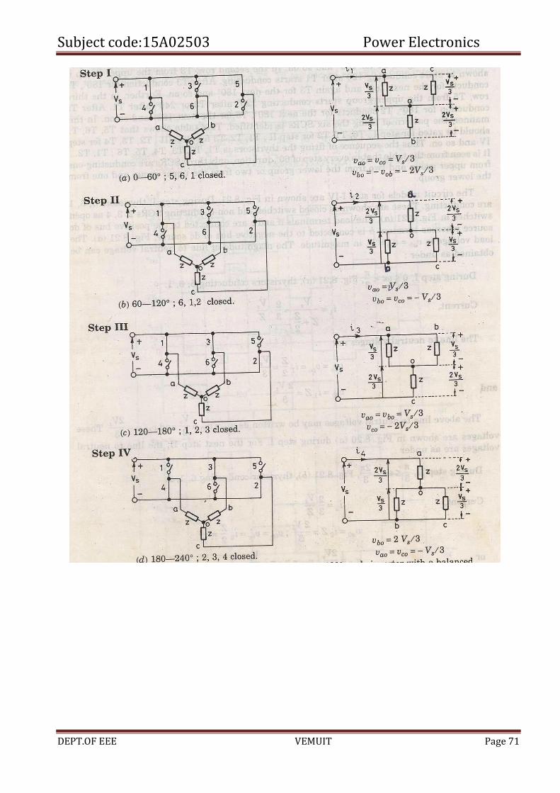
Subject code:15A02503 Power Electronics
DEPT.OF EEE VEMUIT Page 71

Subject code:15A02503 Power Electronics
DEPT.OF EEE VEMUIT Page 72
4,5,6 5,6,1
3,4,5 6,1,2
2,3,4 1,2,3
𝑉𝑅𝑁 𝑉𝑌𝑁 𝑉𝐵𝑁 𝑉𝑅𝑌 𝑉𝑌𝐵 𝑉𝐵𝑅 𝑉1
𝑉
3 −2𝑉
3
𝑉
3
𝑉𝑎𝑐 −𝑉𝑑𝑐 0 2 (3300)
√3
2𝑉
3
−𝑉
3
−𝑉
3
𝑉𝑑𝑐 0 −𝑉𝑑𝑐 2
(300) √3
𝑉3
𝑉
3
−2𝑉
3
0 V -V 2 (900)
√3
−𝑉
3
2𝑉
3
−𝑉
3
-V V 0 2 (1500)
√3
−2𝑉
3
𝑉
3
𝑉
3
-V 0 0 2 (2100)
√3
−𝑉
3
−𝑉
3
2𝑉
3
0 -V 0 2 (2700)
√3
Fourier analysis
If we go for harmonic analysis 𝑉𝑅𝑌=∑∞
4𝑉𝑠𝑖𝑛
𝑛𝜋 sin 𝑛(𝜔𝑡+𝜋⁄ )
𝑛=1,3,5…𝑛𝜋 3 6
Subject code:15A02503 Power Electronics
DEPT.OF EEE VEMUIT Page 73
𝑉 ∑∞
4𝑉𝑆𝑠𝑖𝑛 𝑛𝜋
sin 𝑛(𝜔𝑡−𝜋⁄ ) 𝑌𝐵= 𝑛=1,3,5… 𝑛𝜋 3 2
𝑉 ∑∞
4𝑉𝑆𝑠𝑖𝑛 𝑛𝜋
sin 𝑛(𝜔𝑡−𝜋⁄ ) 𝐵𝑅= 𝑛=1,3,5… 𝑛𝜋 3 6
All even harmonics are zero all triple n harmonics are zero. The
rms nth component of the line voltage is
4𝑉 𝑛𝜋 4𝑉
=√2𝑛𝜋
sin 3
=√2𝜋
sin(60)
For n=1
=0.7797𝑉𝑆
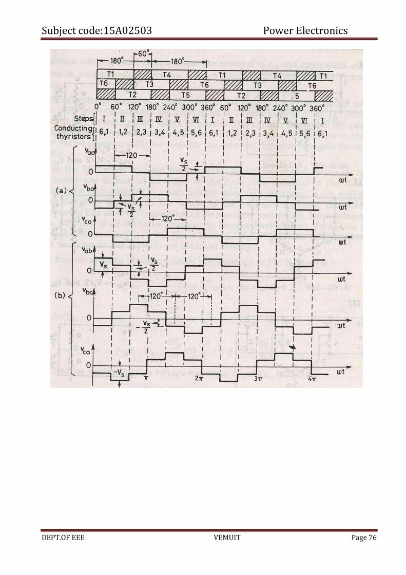
Three phase 1200mode VSI
The circuit diagram is same as that for 1800 mode of conduction.
Here each thyristor conducts for 1200.There are 6 steps each of 600 duration, for completing
one cycle of ac output voltage.
5,6 6,1
4,5 1,2
3,4 2,3
Subject code:15A02503 Power Electronics
DEPT.OF EEE VEMUIT Page 74
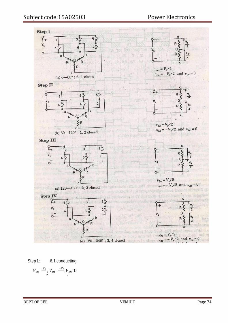
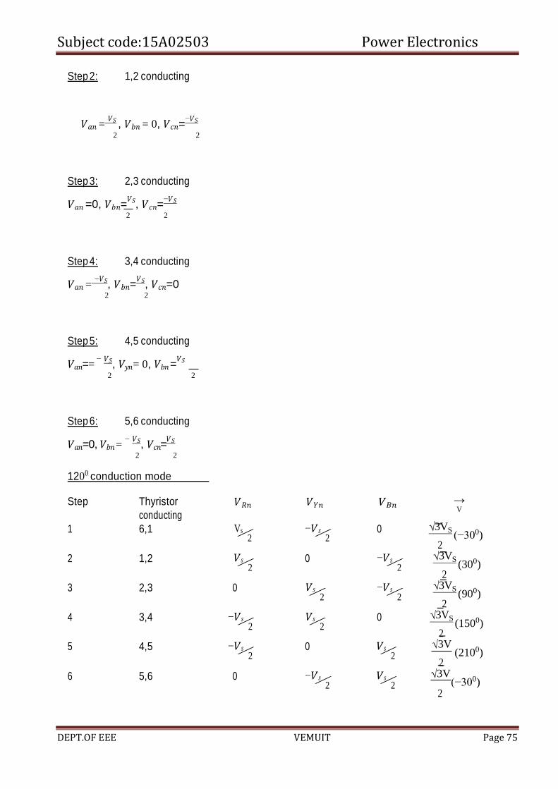
Step 1: 6,1 conducting
𝑉𝑎𝑛 = 𝑉𝑆 , 𝑉𝑦𝑛 =
−𝑉𝑆, 𝑉𝑐𝑛=0 2 2
Subject code:15A02503 Power Electronics
DEPT.OF EEE VEMUIT Page 75
Step 2: 1,2 conducting
𝑉𝑎𝑛 = 𝑉𝑆 , 𝑉𝑏𝑛 = 0, 𝑉𝑐𝑛=
−𝑉𝑆
2 2
Step 3: 2,3 conducting
𝑉𝑎𝑛 =0, 𝑉𝑏𝑛=𝑉𝑆, 𝑉𝑐𝑛=
−𝑉𝑆
2 2
Step 4: 3,4 conducting
𝑉𝑎𝑛 = −𝑉𝑆, 𝑉𝑏𝑛=
𝑉𝑆, 𝑉𝑐𝑛=0 2 2
Step 5: 4,5 conducting
𝑉𝑎𝑛== − 𝑉𝑆, 𝑉𝑦𝑛 = 0, 𝑉𝑏𝑛 =
𝑉𝑆
2 2
Step 6: 5,6 conducting
𝑉𝑎𝑛=0, 𝑉𝑏𝑛 = − 𝑉𝑆, 𝑉𝑐𝑛=
𝑉𝑆
2 2
1200 conduction mode
Step
Thyristor
conducting
𝑉𝑅𝑛
𝑉𝑌𝑛
𝑉𝐵𝑛
→ V
1 6,1 Vs⁄2 −𝑉𝑠⁄
2 0 √3VS
(−300) 2
2 1,2 𝑉𝑠⁄2 0 −𝑉𝑠⁄
2 √3VS
(300) 2
3 2,3 0 𝑉𝑠⁄2 −𝑉𝑠⁄
2 √3VS
(900) 2
4 3,4 −𝑉𝑠⁄2 𝑉𝑠⁄
2 0 √3VS
(1500) 2
5 4,5 −𝑉𝑠⁄2 0 𝑉𝑠⁄
2 √3V
(2100) 2
6 5,6 0 −𝑉𝑠⁄2 𝑉𝑠⁄
2 √3V
(−300) 2
Subject code:15A02503 Power Electronics
DEPT.OF EEE VEMUIT Page 76
Subject code:15A02503 Power Electronics
DEPT.OF EEE VEMUIT Page 77
UNIT-V
AC VOLTAGE CONTROLLERS
&
CYCLO CONVERTERS
Subject code:15A02503 Power Electronics
DEPT.OF EEE VEMUIT Page 78
This lesson provides the reader the following:
(i) AC-AC power conversion topologies at fixed frequency
(ii) Power converter options available for the conversion
(iii) Ability to formulate equations describing the current waveform for the PAC
(iv) Ability sketch the current waveform by observation of the circuit
(v) Ability to assess the performance of the converter of the topologies
Introduction
AC to AC voltage converters operates on the AC mains essentially to regulate the output
voltage. Portions of the supply sinusoid appear at the load while the semiconductor switches
block the remaining portions. Several topologies have emerged along with voltage regulation
methods, most of which are linked to the development of the semiconductor devices.
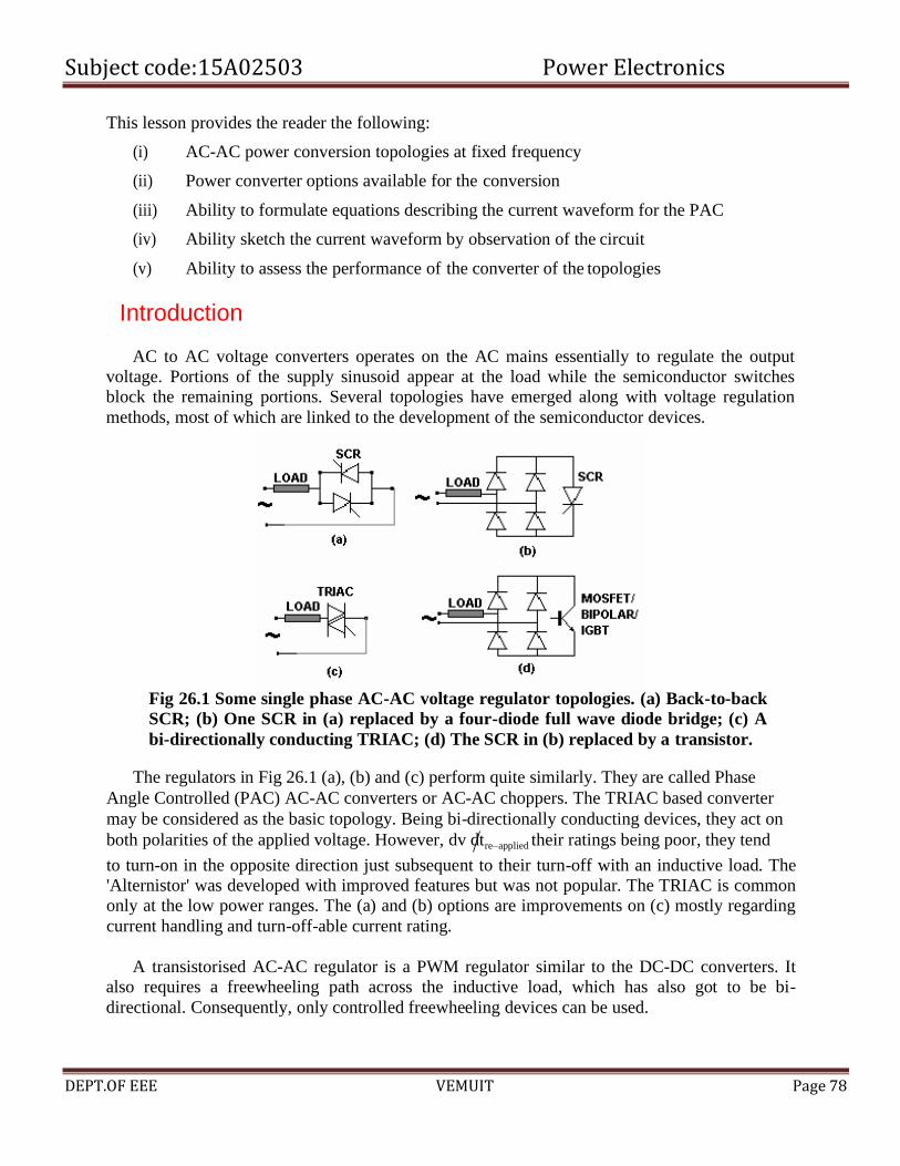
Fig 26.1 Some single phase AC-AC voltage regulator topologies. (a) Back-to-back
SCR; (b) One SCR in (a) replaced by a four-diode full wave diode bridge; (c) A
bi-directionally conducting TRIAC; (d) The SCR in (b) replaced by a transistor.
The regulators in Fig 26.1 (a), (b) and (c) perform quite similarly. They are called Phase
Angle Controlled (PAC) AC-AC converters or AC-AC choppers. The TRIAC based converter
may be considered as the basic topology. Being bi-directionally conducting devices, they act on
both polarities of the applied voltage. However, dv dtre−applied their ratings being poor, they tend
to turn-on in the opposite direction just subsequent to their turn-off with an inductive load. The
'Alternistor' was developed with improved features but was not popular. The TRIAC is common
only at the low power ranges. The (a) and (b) options are improvements on (c) mostly regarding
current handling and turn-off-able current rating.
A transistorised AC-AC regulator is a PWM regulator similar to the DC-DC converters. It
also requires a freewheeling path across the inductive load, which has also got to be bi-
directional. Consequently, only controlled freewheeling devices can be used.
Subject code:15A02503 Power Electronics
DEPT.OF EEE VEMUIT Page 79
Operation with resistive loads
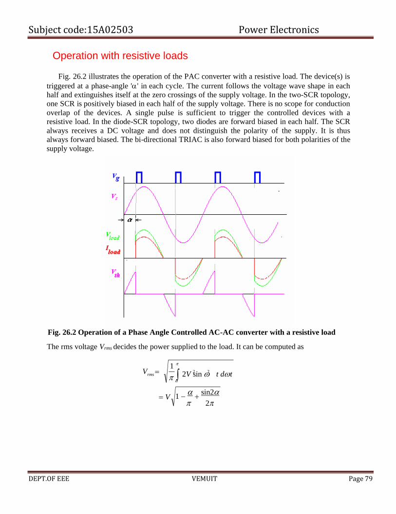
Fig. 26.2 illustrates the operation of the PAC converter with a resistive load. The device(s) is
triggered at a phase-angle '' in each cycle. The current follows the voltage wave shape in each
half and extinguishes itself at the zero crossings of the supply voltage. In the two-SCR topology,
one SCR is positively biased in each half of the supply voltage. There is no scope for conduction
overlap of the devices. A single pulse is sufficient to trigger the controlled devices with a
resistive load. In the diode-SCR topology, two diodes are forward biased in each half. The SCR
always receives a DC voltage and does not distinguish the polarity of the supply. It is thus
always forward biased. The bi-directional TRIAC is also forward biased for both polarities of the
supply voltage.
Fig. 26.2 Operation of a Phase Angle Controlled AC-AC converter with a resistive load
The rms voltage Vrms decides the power supplied to the load. It can be computed as
Vrms =
= V
1
2V sin 2 2
t dt
1 −
+ sin2
2
Subject code:15A02503 Power Electronics
DEPT.OF EEE VEMUIT Page 80
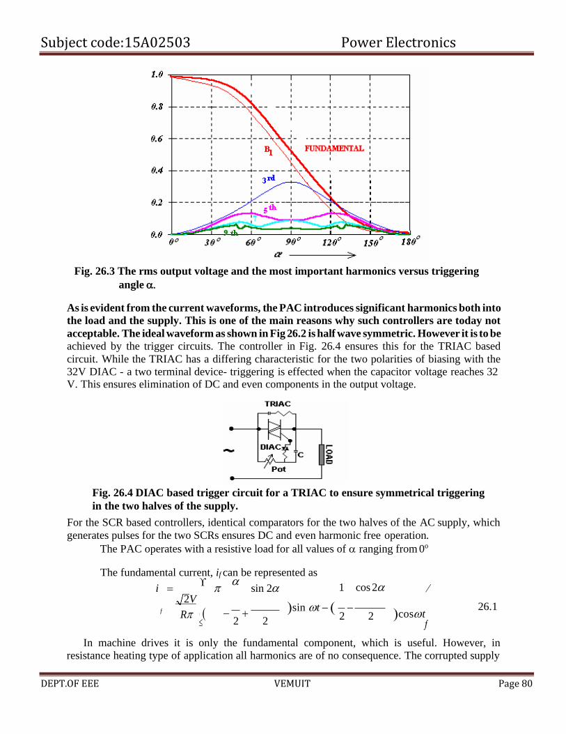
Fig. 26.3 The rms output voltage and the most important harmonics versus triggering
angle
As is evident from the current waveforms, the PAC introduces significant harmonics both into
the load and the supply. This is one of the main reasons why such controllers are today not
acceptable. The ideal waveform as shown in Fig 26.2 is half wave symmetric. However it is to be
achieved by the trigger circuits. The controller in Fig. 26.4 ensures this for the TRIAC based
circuit. While the TRIAC has a differing characteristic for the two polarities of biasing with the
32V DIAC - a two terminal device- triggering is effected when the capacitor voltage reaches 32 V. This ensures elimination of DC and even components in the output voltage.
Fig. 26.4 DIAC based trigger circuit for a TRIAC to ensure symmetrical triggering
in the two halves of the supply.
For the SCR based controllers, identical comparators for the two halves of the AC supply, which
generates pulses for the two SCRs ensures DC and even harmonic free operation.
The PAC operates with a resistive load for all values of ranging from 0o
The fundamental current, if can be represented as
i =
sin 2 1 cos 2 2V
R ( −
2 +
2
)sin t − ( 2
− 2 )cost
26.1
In machine drives it is only the fundamental component, which is useful. However, in
resistance heating type of application all harmonics are of no consequence. The corrupted supply
f

Subject code:15A02503 Power Electronics
DEPT.OF EEE VEMUIT Page 81
current nevertheless is undesirable.
Subject code:15A02503 Power Electronics
DEPT.OF EEE VEMUIT Page 82
Power Factor
The power factor of a nonlinear deserves a special discussion. Fig. 26.2 shows the supply
voltage and the non-sinusoidal load current. The fundamental load/supply current lags the
supply voltage by the , 'Fundamental Power Factor' angle. Cos is also called the
'Displacement Factor'. However this does not account for the total reactive power drawn by the
system. This power factor is inspite of the actual load being resistive! The reactive power is
drawn also y the trigger-angle dependent harmonics. Now
power factor = average power =
P 26.2
apparent voltamperes VIL
= VIL1 cos1
VIL
distortion factor = IL1
IL
The Average Power, P drawn by the resistive load is 1 2 1 2V
2 2
26.3
P = 2 0
viL dt =
= 2V
2
sin 2
R
− 2
+ 2
sin R
t dwt
The portion within square brackets in Eq. 26.5 is identical to the first part of the expression within brackets in Eq. 26.1, which is called the Fourier coefficient 'BB1'. The rms load
voltage can also be similarly obtained by integrating between and and the result can be
combined with Eq. 26.5 to give
power factor = per − unit
=
rms load − current
per − unit load power
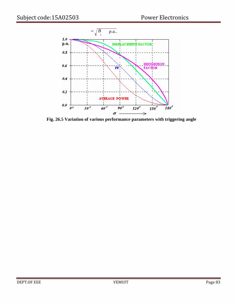
Subject code:15A02503 Power Electronics
DEPT.OF EEE VEMUIT Page 83
Fig. 26.5 Variation of various performance parameters with triggering angle
= B 1
p.u..
Subject code:15A02503 Power Electronics
DEPT.OF EEE VEMUIT Page 84
Operation with inductive loads
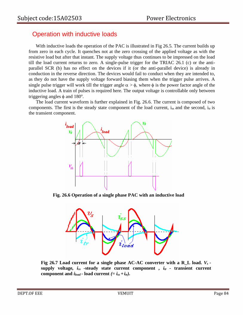
With inductive loads the operation of the PAC is illustrated in Fig 26.5. The current builds up
from zero in each cycle. It quenches not at the zero crossing of the applied voltage as with the
resistive load but after that instant. The supply voltage thus continues to be impressed on the load
till the load current returns to zero. A single-pulse trigger for the TRIAC 26.1 (c) or the anti-
parallel SCR (b) has no effect on the devices if it (or the anti-parallel device) is already in
conduction in the reverse direction. The devices would fail to conduct when they are intended to,
as they do not have the supply voltage forward biasing them when the trigger pulse arrives. A
single pulse trigger will work till the trigger angle > where is the power factor angle of the
inductive load. A train of pulses is required here. The output voltage is controllable only between
triggering angles and 180o.
The load current waveform is further explained in Fig. 26.6. The current is composed of two
components. The first is the steady state component of the load current, iss and the second, itr is
the transient component.
Fig. 26.6 Operation of a single phase PAC with an inductive load
Fig 26.7 Load current for a single phase AC-AC converter with a R_L load. Vs -
supply voltage, iss -steady state current component , itr - transient current
component and iload - load current (= iss + itr).
Subject code:15A02503 Power Electronics
DEPT.OF EEE VEMUIT Page 85
)
With an inductance in the load the distinguishing feature of the load current is that it must
always start from zero. However, if the switch could have permanently kept the load connected
to the supply the current would have become a sinusoidal one phase shifted from the voltage by
the phase angle of the load, This current restricted to the half periods of conduction is called
the 'steady-state component' of load current iss. The 'transient component' of load current itr, again
in each half cycle, must add up to zero with this iss to start from zero. This condition sets the
initial value of the transient component to that of the steady state at the instant that the
SCR/TRIAC is triggered. Fig. 26.6 illustrates these relations.
When a device is in conduction, the load current is governed by the equation
L di dt
+ Ri =vs
iload
2V =
Z
( ) ( − R (
−t )
sin t − + sin − e L
Since at t = 0, iload = 0 and supply voltage vs = Vsint the solution is of the form
The instant when the load current extinguishes is called the extinction angle . It can be
inferred that there would be no transients in the load current if the devices are triggered at the
power factor angle of the load. The load current I that case is perfectly sinusoidal.
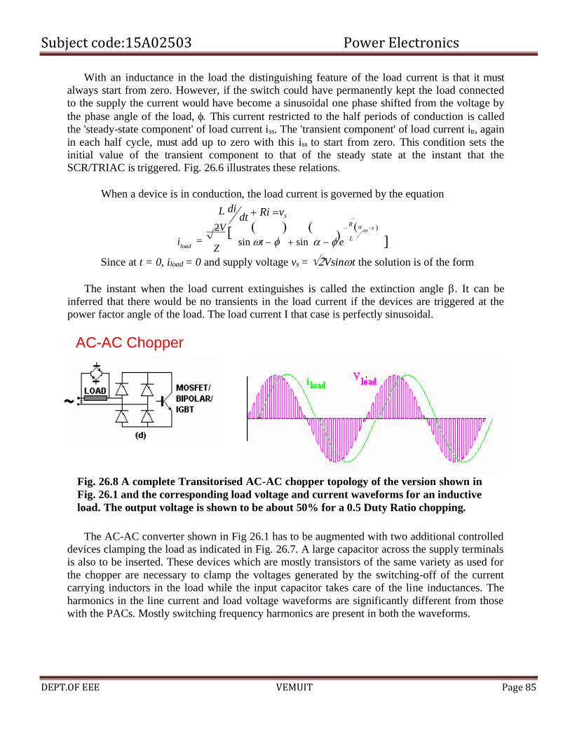
AC-AC Chopper
Fig. 26.8 A complete Transitorised AC-AC chopper topology of the version shown in
Fig. 26.1 and the corresponding load voltage and current waveforms for an inductive
load. The output voltage is shown to be about 50% for a 0.5 Duty Ratio chopping.
The AC-AC converter shown in Fig 26.1 has to be augmented with two additional controlled
devices clamping the load as indicated in Fig. 26.7. A large capacitor across the supply terminals
is also to be inserted. These devices which are mostly transistors of the same variety as used for
the chopper are necessary to clamp the voltages generated by the switching-off of the current
carrying inductors in the load while the input capacitor takes care of the line inductances. The
harmonics in the line current and load voltage waveforms are significantly different from those
with the PACs. Mostly switching frequency harmonics are present in both the waveforms.
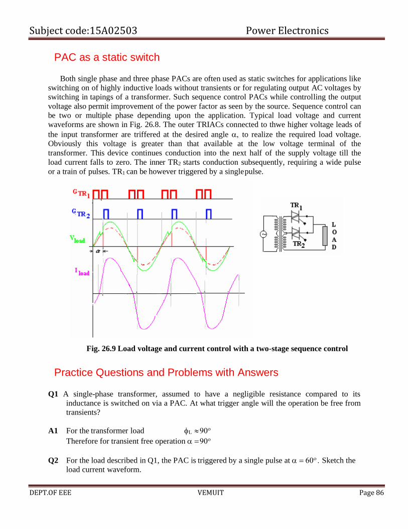
Subject code:15A02503 Power Electronics
DEPT.OF EEE VEMUIT Page 86
PAC as a static switch
Both single phase and three phase PACs are often used as static switches for applications like
switching on of highly inductive loads without transients or for regulating output AC voltages by
switching in tapings of a transformer. Such sequence control PACs while controlling the output
voltage also permit improvement of the power factor as seen by the source. Sequence control can
be two or multiple phase depending upon the application. Typical load voltage and current
waveforms are shown in Fig. 26.8. The outer TRIACs connected to thwe higher voltage leads of
the input transformer are triffered at the desired angle to realize the required load voltage.
Obviously this voltage is greater than that available at the low voltage terminal of the
transformer. This device continues conduction into the next half of the supply voltage till the
load current falls to zero. The inner TR2 starts conduction subsequently, requiring a wide pulse
or a train of pulses. TR1 can be however triggered by a single pulse.
Fig. 26.9 Load voltage and current control with a two-stage sequence control
Practice Questions and Problems with Answers
Q1 A single-phase transformer, assumed to have a negligible resistance compared to its
inductance is switched on via a PAC. At what trigger angle will the operation be free from
transients?
A1 For the transformer load L
Therefore for transient free operation =
Q2 For the load described in Q1, the PAC is triggered by a single pulse at = Sketch the
load current waveform.
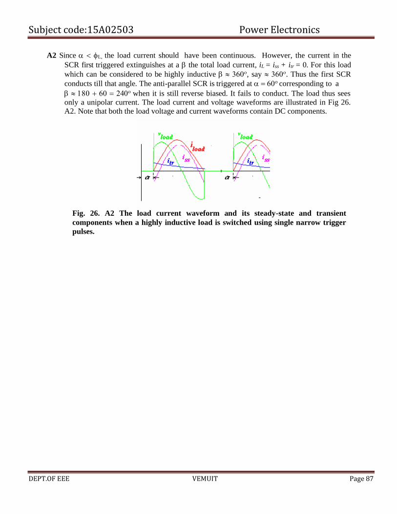
Subject code:15A02503 Power Electronics
DEPT.OF EEE VEMUIT Page 87
A2 Since L, the load current should have been continuous. However, the current in the
SCR first triggered extinguishes at a the total load current, iL = iss + itr = 0. For this load
which can be considered to be highly inductive , say . Thus the first SCR
conducts till that angle. The anti-parallel SCR is triggered at = corresponding to a
+ = when it is still reverse biased. It fails to conduct. The load thus sees
only a unipolar current. The load current and voltage waveforms are illustrated in Fig 26.
A2. Note that both the load voltage and current waveforms contain DC components.
Fig. 26. A2 The load current waveform and its steady-state and transient
components when a highly inductive load is switched using single narrow trigger
pulses.
Subject code:15A02503 Power Electronics
DEPT.OF EEE VEMUIT Page 88
CYCLO CONVERTERS
Subject code:15A02503 Power Electronics
DEPT.OF EEE VEMUIT Page 89
Instructional Objectives
Study of the following:
• The cyclo-converter circuits − basic principle of operation
• The circuit for the single-phase to single-phase cyclo-converter using thyristors
• The operation of the above cyclo-converter circuit, along with the voltage waveforms
Introduction
Earlier in the last three (4.1-4.3) lessons (first half) of this module, the circuit and operation
of ac to ac voltage controllers − both single-phase and three-phase, were described in detail. The
devices used are either triac, or thyristors connected back to back. In this lesson (4.4) − first one
in the second half of this module, the cyclo-converter is introduced as a type of power controller,
where an alternating voltage at supply frequency is converted directly to an alternating voltage at
load frequency (normally lower), without any intermediate dc stage. As will be shown in the last
(fifth) module, an alternating voltage at any frequency (output) is obtained using an inverter as a
power controller from a dc voltage fed at its input. This input, i.e. dc voltage, is again obtained
using a rectifier (converter) with ac voltage (normally at supply frequency) fed at its input. This
type has been described in module 2. Note that this is a two-stage process with an intermediate
dc stage. Now-a-days, the power switching devices used in the inverter circuit belong to
transistor family (termed as self-commutated ones), starting with power transistors, whereas
thyristors are still being used in the converter (rectifier) circuits. These devices are called force-
commutated ones, when used in dc chopper circuits (described in module 3), but in this case, i.e.
converter circuits, line commutation takes place. As stated earlier, the output frequency of the
cyclo-converter is limited to about one-third of supply (line) frequency of 50 Hz.
Initially, the basic principle of operation used in a cyclo-converter is discussed. Then, the
circuit of a single-phase to single-phase cyclo-converter using thyristors is presented. This is
followed by describing the operation of the above cyclo-converter circuit, along with voltage
waveforms. The readers at this stage, have gone through the following lessons − single-phase
fully controlled converter using thyristors, for obtaining dc output voltage from ac supply (#2.2),
and ac to ac voltage controllers − both single-phase and three-phase, using either triac, or
thyristors connected back to back (#4.1-4.3). In the above cases, the output voltage obtained is,
in the form of phase-controlled one, as can be observed from the waveforms shown in the above
lessons. In the present case, the output voltage of the cyclo-converter circuit (single-phase) using
thyristors, is synthesized from the above phase-controlled voltage waveforms, so as to obtain an
ac waveform (output) of low frequency, with the input being an ac voltage of higher frequency,
say line. The angle, at which the thyristors are triggered, is controlled to obtain the desired
waveform.
Keywords: Single-phase to single-phase cyclo-converter using thyristors, Voltage waveforms.
Cyclo-converter
Basic Principle of Operation

Subject code:15A02503 Power Electronics
DEPT.OF EEE VEMUIT Page 90
The basic principle of operation of a cyclo-converter is explained with reference to an equivalent circuit shown in Fig. 29.1. Each two-quadrant converter (phase-controlled) is
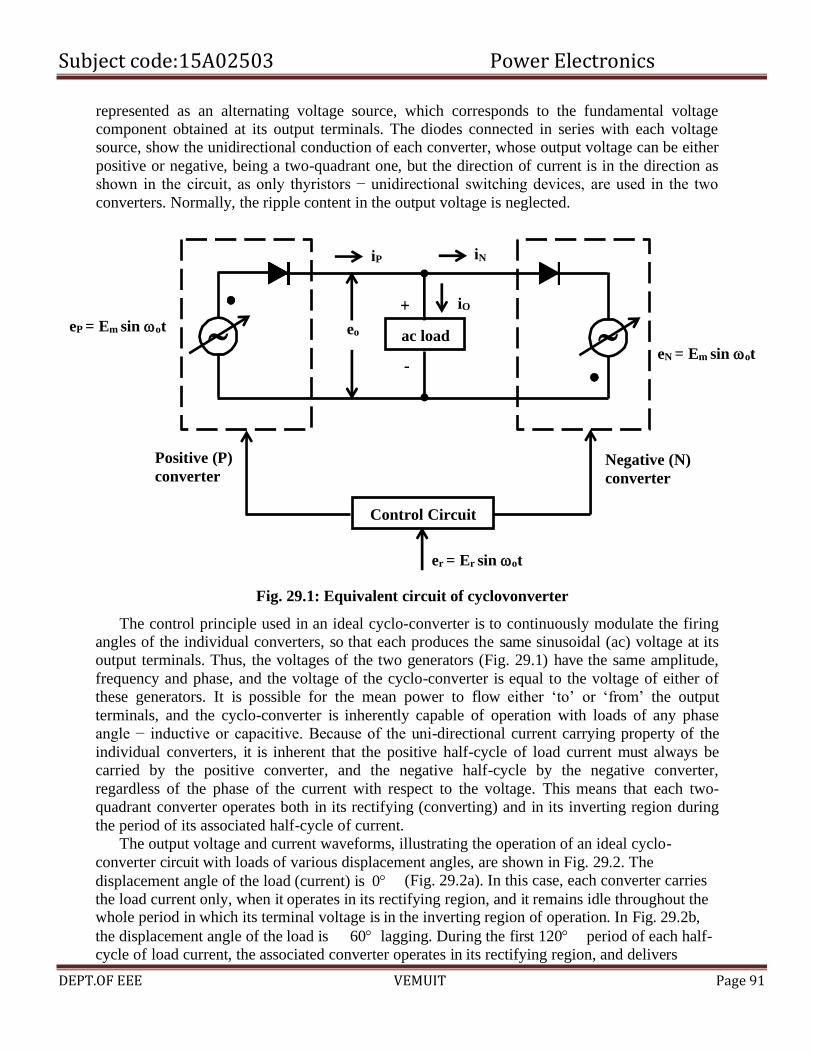
Subject code:15A02503 Power Electronics
DEPT.OF EEE VEMUIT Page 91
eo
iO +
ac load
represented as an alternating voltage source, which corresponds to the fundamental voltage
component obtained at its output terminals. The diodes connected in series with each voltage
source, show the unidirectional conduction of each converter, whose output voltage can be either
positive or negative, being a two-quadrant one, but the direction of current is in the direction as
shown in the circuit, as only thyristors − unidirectional switching devices, are used in the two
converters. Normally, the ripple content in the output voltage is neglected.
eP = Em sin ot
iP iN
eN = Em sin ot
Positive (P)
converter Negative (N)
converter
er = Er sin ot
Fig. 29.1: Equivalent circuit of cyclovonverter
The control principle used in an ideal cyclo-converter is to continuously modulate the firing
angles of the individual converters, so that each produces the same sinusoidal (ac) voltage at its
output terminals. Thus, the voltages of the two generators (Fig. 29.1) have the same amplitude,
frequency and phase, and the voltage of the cyclo-converter is equal to the voltage of either of
these generators. It is possible for the mean power to flow either ‘to’ or ‘from’ the output
terminals, and the cyclo-converter is inherently capable of operation with loads of any phase
angle − inductive or capacitive. Because of the uni-directional current carrying property of the
individual converters, it is inherent that the positive half-cycle of load current must always be
carried by the positive converter, and the negative half-cycle by the negative converter,
regardless of the phase of the current with respect to the voltage. This means that each two-
quadrant converter operates both in its rectifying (converting) and in its inverting region during
the period of its associated half-cycle of current.
The output voltage and current waveforms, illustrating the operation of an ideal cyclo-
converter circuit with loads of various displacement angles, are shown in Fig. 29.2. The
displacement angle of the load (current) is 0 (Fig. 29.2a). In this case, each converter carries
the load current only, when it operates in its rectifying region, and it remains idle throughout the whole period in which its terminal voltage is in the inverting region of operation. In Fig. 29.2b,
the displacement angle of the load is 60 lagging. During the first 120 period of each half-
cycle of load current, the associated converter operates in its rectifying region, and delivers
Control Circuit
-

Subject code:15A02503 Power Electronics
DEPT.OF EEE VEMUIT Page 92
power to the load. During the latter 60 period in the half-cycle, the associated converter
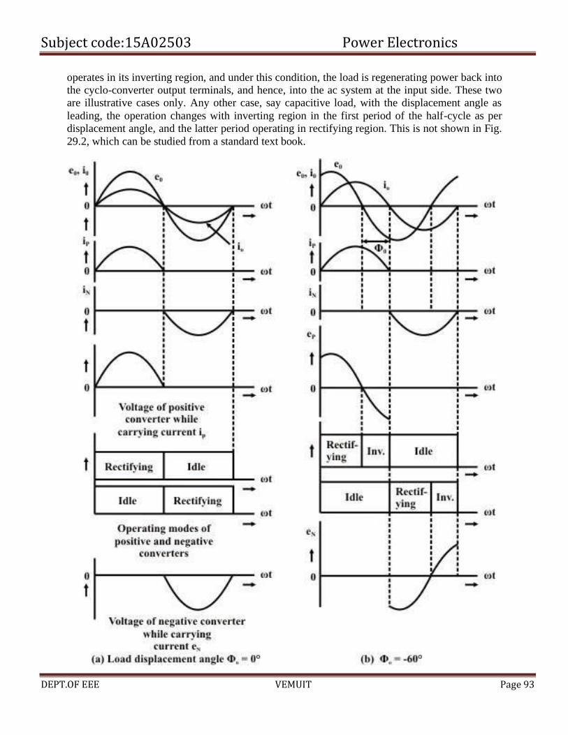
Subject code:15A02503 Power Electronics
DEPT.OF EEE VEMUIT Page 93
operates in its inverting region, and under this condition, the load is regenerating power back into
the cyclo-converter output terminals, and hence, into the ac system at the input side. These two
are illustrative cases only. Any other case, say capacitive load, with the displacement angle as
leading, the operation changes with inverting region in the first period of the half-cycle as per
displacement angle, and the latter period operating in rectifying region. This is not shown in Fig.
29.2, which can be studied from a standard text book.
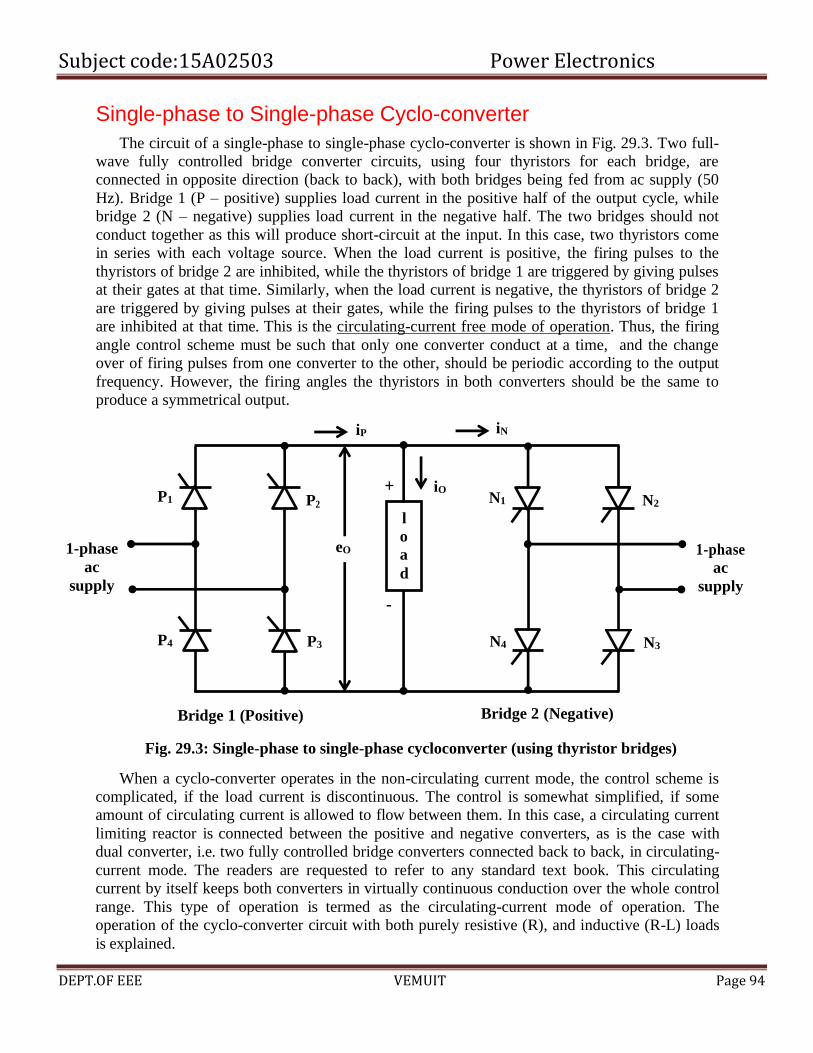
Subject code:15A02503 Power Electronics
DEPT.OF EEE VEMUIT Page 94
Single-phase to Single-phase Cyclo-converter
The circuit of a single-phase to single-phase cyclo-converter is shown in Fig. 29.3. Two full-
wave fully controlled bridge converter circuits, using four thyristors for each bridge, are
connected in opposite direction (back to back), with both bridges being fed from ac supply (50
Hz). Bridge 1 (P – positive) supplies load current in the positive half of the output cycle, while
bridge 2 (N – negative) supplies load current in the negative half. The two bridges should not
conduct together as this will produce short-circuit at the input. In this case, two thyristors come
in series with each voltage source. When the load current is positive, the firing pulses to the
thyristors of bridge 2 are inhibited, while the thyristors of bridge 1 are triggered by giving pulses
at their gates at that time. Similarly, when the load current is negative, the thyristors of bridge 2
are triggered by giving pulses at their gates, while the firing pulses to the thyristors of bridge 1
are inhibited at that time. This is the circulating-current free mode of operation. Thus, the firing
angle control scheme must be such that only one converter conduct at a time, and the change
over of firing pulses from one converter to the other, should be periodic according to the output
frequency. However, the firing angles the thyristors in both converters should be the same to
produce a symmetrical output.
1-phase
ac
supply
1-phase
ac
supply
Bridge 1 (Positive) Bridge 2 (Negative)
Fig. 29.3: Single-phase to single-phase cycloconverter (using thyristor bridges)
When a cyclo-converter operates in the non-circulating current mode, the control scheme is
complicated, if the load current is discontinuous. The control is somewhat simplified, if some
amount of circulating current is allowed to flow between them. In this case, a circulating current
limiting reactor is connected between the positive and negative converters, as is the case with
dual converter, i.e. two fully controlled bridge converters connected back to back, in circulating-
current mode. The readers are requested to refer to any standard text book. This circulating
current by itself keeps both converters in virtually continuous conduction over the whole control
range. This type of operation is termed as the circulating-current mode of operation. The
operation of the cyclo-converter circuit with both purely resistive (R), and inductive (R-L) loads
is explained.
iP iN
P1 P + iO
2 N1 N2
eO
-
P4 P3 N4 N3
l
o
a
d

Subject code:15A02503 Power Electronics
DEPT.OF EEE VEMUIT Page 95
Resistive (R) Load: For this load, the load current (instantaneous) goes to zero, as the input
voltage at the end of each half cycle (both positive and negative) reaches zero (0). Thus, the
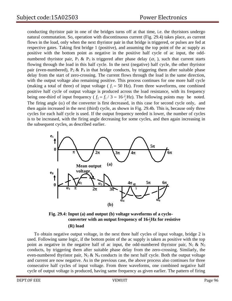
Subject code:15A02503 Power Electronics
DEPT.OF EEE VEMUIT Page 96
0 5
2 3 4 6
3
3
conducting thyristor pair in one of the bridges turns off at that time, i.e. the thyristors undergo
natural commutation. So, operation with discontinuous current (Fig. 29.4) takes place, as current
flows in the load, only when the next thyristor pair in that bridge is triggered, or pulses are fed at
respective gates. Taking first bridge 1 (positive), and assuming the top point of the ac supply as
positive with the bottom point as negative in the positive half cycle of ac input, the odd-
numbered thyristor pair, P1 & P3 is triggered after phase delay (1 ), such that current starts
flowing through the load in this half cycle. In the next (negative) half cycle, the other thyristor
pair (even-numbered), P2 & P4 in that bridge conducts, by triggering them after suitable phase
delay from the start of zero-crossing. The current flows through the load in the same direction,
with the output voltage also remaining positive. This process continues for one more half cycle
(making a total of three) of input voltage ( f1 = 50 Hz). From three waveforms, one combined
positive half cycle of output voltage is produced across the load resistance, with its frequency
being one-third of input frequency ( f2 = f1 / 3 = 16 2 Hz). The following points may be noted.
The firing angle () of the converter is first decreased, in this case for second cycle only, and
then again increased in the next (third) cycle, as shown in Fig. 29.4b. This is, because only three
cycles for each half cycle is used. If the output frequency needed is lower, the number of cycles
is to be increased, with the firing angle decreasing for some cycles, and then again increasing in
the subsequent cycles, as described earlier.
es
Mean output
e0 voltage
(a)
0 α2 α3 4 α 5 6
α1 2 3
(b)
5
α4 α6
Fig. 29.4: Input (a) and output (b) voltage waveforms of a cyclo-
converter with an output frequency of 16 2 Hz for resistive
(R) load
To obtain negative output voltage, in the next three half cycles of input voltage, bridge 2 is
used. Following same logic, if the bottom point of the ac supply is taken as positive with the top
point as negative in the negative half of ac input, the odd-numbered thyristor pair, N1 & N3
conducts, by triggering them after suitable phase delay from the zero-crossing. Similarly, the
even-numbered thyristor pair, N2 & N4 conducts in the next half cycle. Both the output voltage
and current are now negative. As in the previous case, the above process also continues for three
consecutive half cycles of input voltage. From three waveforms, one combined negative half
cycle of output voltage is produced, having same frequency as given earlier. The pattern of firing

Subject code:15A02503 Power Electronics
DEPT.OF EEE VEMUIT Page 97
angle − first decreasing and the increasing, is also followed in the negative half cycle. One
positive half cycle, along with one negative half cycle, constitute one complete cycle of output
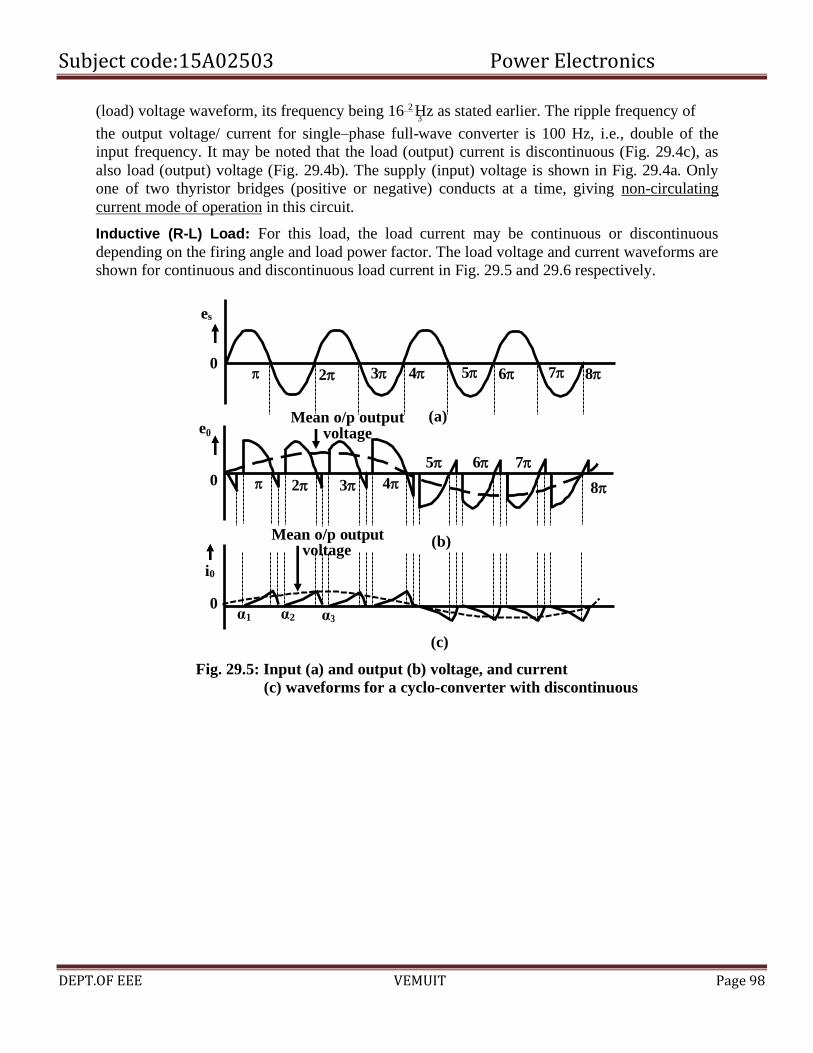
Subject code:15A02503 Power Electronics
DEPT.OF EEE VEMUIT Page 98
2 3 4 5 6 7 8
3 (load) voltage waveform, its frequency being 16 2 Hz as stated earlier. The ripple frequency of
the output voltage/ current for single–phase full-wave converter is 100 Hz, i.e., double of the
input frequency. It may be noted that the load (output) current is discontinuous (Fig. 29.4c), as
also load (output) voltage (Fig. 29.4b). The supply (input) voltage is shown in Fig. 29.4a. Only
one of two thyristor bridges (positive or negative) conducts at a time, giving non-circulating
current mode of operation in this circuit.
Inductive (R-L) Load: For this load, the load current may be continuous or discontinuous
depending on the firing angle and load power factor. The load voltage and current waveforms are
shown for continuous and discontinuous load current in Fig. 29.5 and 29.6 respectively.
es
0
Mean o/p output 0
(a)
Mean o/p output voltage
i0
(b)
0 α1 α2 α
(c)
Fig. 29.5: Input (a) and output (b) voltage, and current
(c) waveforms for a cyclo-converter with discontinuous
voltage
5 6 7 0 2 3 4 8
3
e
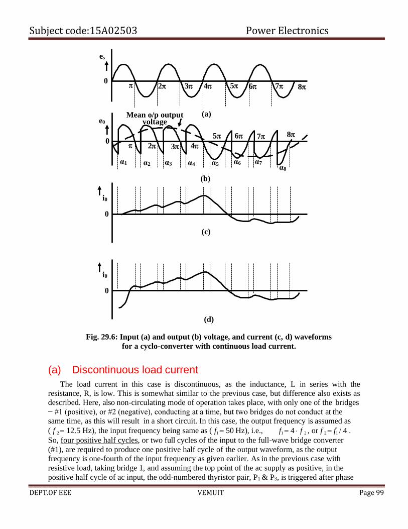
Subject code:15A02503 Power Electronics
DEPT.OF EEE VEMUIT Page 99
es
0
e0
(b)
i0
0
i0
0
Fig. 29.6: Input (a) and output (b) voltage, and current (c, d) waveforms
for a cyclo-converter with continuous load current.
(a) Discontinuous load current
The load current in this case is discontinuous, as the inductance, L in series with the
resistance, R, is low. This is somewhat similar to the previous case, but difference also exists as
described. Here, also non-circulating mode of operation takes place, with only one of the bridges
− #1 (positive), or #2 (negative), conducting at a time, but two bridges do not conduct at the
same time, as this will result in a short circuit. In this case, the output frequency is assumed as
( f 2 = 12.5 Hz), the input frequency being same as ( f1 = 50 Hz), i.e., f1 = 4 f 2 , or f 2 = f1 / 4 .
So, four positive half cycles, or two full cycles of the input to the full-wave bridge converter
(#1), are required to produce one positive half cycle of the output waveform, as the output
frequency is one-fourth of the input frequency as given earlier. As in the previous case with
resistive load, taking bridge 1, and assuming the top point of the ac supply as positive, in the
positive half cycle of ac input, the odd-numbered thyristor pair, P1 & P3, is triggered after phase
(c)
Mean o/p output voltage
(a)
0 5 6 7 8
α1
2 3 4
α2 α3 α4 α5 α6 α7 α8
(d)
2 3 4 5 6 7 8

Subject code:15A02503 Power Electronics
DEPT.OF EEE VEMUIT Page 100
delay ( = t = 1 ), such that current starts flowing the inductive load in this half cycle. But
Subject code:15A02503 Power Electronics
DEPT.OF EEE VEMUIT Page 101
here, the current flows even after the input voltage has reversed (after = ), till it reaches zero
at ( = 1 ) with ( + 2) 1 , due to inductance being present in series with resistance, its
value being low. It may be noted that the thyristor pair is, thus, naturally commutated. In the next
(negative) half cycle, the other thyristor pair (even-numbered), P2 & P4, is triggered at ( + 2) .
The current flows through the load in the same direction, with the output voltage also remaining
positive. The current goes to zero at ( + 2) , with ( + 3) 2 . This procedure continues
for the next two half cycles, making a total of four positive half cycles. From these four
waveforms, one combined positive half cycle of output voltage is produced across the inductive
load. The firing angle () of the converter is first decreased, in this case for second half cycle
only, kept nearly same in the third one, and finally increased in the last (fourth) one, as shown in
Fig. 29.5b.
To obtain negative output voltage, in the next four half cycles of output voltage, bridge 2 is
used. Following same logic, if the bottom point of the ac supply is taken as positive in the
negative half of ac input, the odd-numbered thyristor pair, N1 & N3 conducts, by triggering them
after phase delay ( = 4 + 1 ). The current flows now in the opposite (negative) direction
through the inductive load, with the output voltage being also negative. The current goes to zero
at ( 4 + 1 ), due to load being inductive as given earlier. Similarly, the even-numbered
thyristor pair, N2 & N4 conducts in the next half cycle, after they are triggered at ( 5 + 2 ). The
current goes to zero at ( 5 + 2 ). Both the output voltage and current are now negative. As in
the previous case, the above process also continues for two more half cycles of input voltage,
making a total of four. From these four waveforms, one combined negative half cycle of output
voltage is produced with same output frequency. The pattern of firing angle − first decreasing and then increasing, is also followed in the negative half cycle. It may be noted that the load
(output) current is discontinuous (Fig. 29.5c), as also load (output) voltage (Fig. 29.5b). The
supply (input) voltage is shown in Fig. 29.5a. One positive half cycle, along with one negative
half cycle, constitute one complete cycle of output (load) voltage waveform, its frequency being
12.5 Hz as stated earlier. The ripple frequency remains also same at 100 Hz, with the ripple in
load current being filtered by the inductance present in the load.
(b) Continuous load current
As given above, the load current is discontinuous, as the inductance of the load is low. If the
inductance is increased, the current will be continuous. Most of the points given earlier are
applicable to this case, as described. To repeat, non-circulating mode of operation is used, i.e.,
only one of the bridges − #1 (positive), or #2 (negative), conducts at a time, but two bridges do
not conduct at the same time, as this will result in a short circuit. Also, the ripple frequency in the voltage and current waveforms remains same at 100 Hz. The output frequency is one-fourth of
input frequency (50 Hz), i.e., 12.5 Hz. So, for each half-cycle of output voltage waveform, four
half cycles of input supply are required. Taking bridge 1, and assuming the top point of the ac
supply as positive, in the positive half cycle of ac input, the odd-numbered thyristor pair, P1 &
P3, is triggered after phase delay ( = t = 1 ), such that current starts flowing the inductive
load in this half cycle. But here, the current flows for about one complete half cycle, i.e., up to
the angle, ( + 1 ) or ( + 2 ), whichever is higher, even after the input voltage has reversed,
due to the high value of load inductance. In the next (negative) half cycle, the other thyristor pair
(even-numbered), P2 & P4, is triggered at ( + 2) . At that time, reverse voltage is applied across

Subject code:15A02503 Power Electronics
DEPT.OF EEE VEMUIT Page 102
each of the conducting thyristors, P1/P3, and the thyristors turn off. The current flows through the
load in the same direction, with the output voltage also remaining positive. Also, the current
Subject code:15A02503 Power Electronics
DEPT.OF EEE VEMUIT Page 103
flows for about one complete half cycle, i.e., up to the angle, ( + 2 ) or ( + 3 ), whichever is
higher. This procedure continues for the next two half cycles, making a total of four positive half
cycles. From these four waveforms, one combined positive half cycle of output voltage is
produced across the inductive load. The firing angle () of the converter is first decreased, in this
case for second half cycle only, kept nearly same in the third one, and finally increased in the last
(fourth) one, as shown in Fig. 29.6b.
To obtain negative output voltage, in the next four half cycles of output voltage, bridge 2 is
used. Following same logic, if the bottom point of the ac supply is taken as positive in the negative half of ac input, the odd-numbered thyristor pair, N1 & N3 conducts, by triggering them
after phase delay ( = 4 + 1 ). The current flows now in the opposite (negative) direction
through the inductive load, with the output voltage being also negative. The current flows for
about one complete half cycle, i.e., up to the angle, ( 5 . + 1 ) or ( 5 + 2 ), whichever is
higher, as the load is inductive. Similarly, the even-numbered thyristor pair, N2 & N4 conducts in
the next half cycle, after they are triggered at ( 5 + 2 ). As described earlier, both the
conducting thyristors turn off, as reverse voltage is applied across each of them. Both the output
voltage and current are now negative. Also, the current flows for about one complete half cycle,
i.e. up to the angle, ( 5 + 2 ) or ( 5 + 3 ), whichever is higher. As in the previous case, the
above process also continues for two more half cycles of input voltage, making a total of four.
From these four waveforms, one combined negative half cycle of output voltage is produced
with same output frequency of 12.5 Hz. The pattern of firing angle − first decreasing and then
increasing, is also followed in the negative half cycle. It may be observed that the load (output)
current is continuous (Fig. 29.6c), as also load (output) voltage (Fig. 29.6b). The load (output)
current is redrawn in Fig. 29.6d, under steady state condition, while the supply (input) voltage is
shown in Fig. 29.6a. One positive half cycle, along with one negative half cycle, constitute one
complete cycle of output (load) voltage waveform.
Advantages and Disadvantages of Cyclo-converter
Advantages
1. In a cyclo-converter, ac power at one frequency is converted directly to a lower frequency in
a single conversion stage.
2. Cyclo-converter functions by means of phase commutation, without auxiliary forced commutation circuits. The power circuit is more compact, eliminating circuit losses
associated with forced commutation.
3. Cyclo-converter is inherently capable of power transfer in either direction between source
and load. It can supply power to loads at any power factor, and is also capable of
regeneration over the complete speed range, down to standstill. This feature makes it
preferable for large reversing drives requiring rapid acceleration and deceleration, thus suited
for metal rolling application.
4. Commutation failure causes a short circuit of ac supply. But, if an individual fuse blows off,
a complete shutdown is not necessary, and cyclo-converter continues to function with
somewhat distorted waveforms. A balanced load is presented to the ac supply with
unbalanced output conditions.
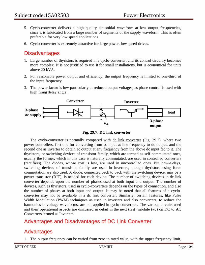
Subject code:15A02503 Power Electronics
DEPT.OF EEE VEMUIT Page 104
5. Cyclo-converter delivers a high quality sinusoidal waveform at low output fre-quencies,
since it is fabricated from a large number of segments of the supply waveform. This is often
preferable for very low speed applications.
6. Cyclo-converter is extremely attractive for large power, low speed drives.
Disadvantages
1. Large number of thyristors is required in a cyclo-converter, and its control circuitry becomes
more complex. It is not justified to use it for small installations, but is economical for units
above 20 kVA.
2. For reasonable power output and efficiency, the output frequency is limited to one-third of
the input frequency.
3. The power factor is low particularly at reduced output voltages, as phase control is used with
high firing delay angle.
3-phase
ac supply
Converter +
-
Vdc
Inverter
3-phase
output
Fig. 29.7: DC link converter
The cyclo-converter is normally compared with dc link converter (Fig. 29.7), where two
power controllers, first one for converting from ac input at line frequency to dc output, and the
second one as inverter to obtain ac output at any frequency from the above dc input fed to it. The
thyristors, or switching devices of transistor family, which are termed as self-commutated ones,
usually the former, which in this case is naturally commutated, are used in controlled converters
(rectifiers). The diodes, whose cost is low, are used in uncontrolled ones. But now-a-days,
switching devices of transistor family are used in inverters, though thyristors using force
commutation are also used. A diode, connected back to back with the switching device, may be a
power transistor (BJT), is needed for each device. The number of switching devices in dc link
converter depends upon the number of phases used at both input and output. The number of
devices, such as thyristors, used in cyclo-converters depends on the types of connection, and also
the number of phases at both input and output. It may be noted that all features of a cyclo-
converter may not be available in a dc link converter. Similarly, certain features, like Pulse
Width Modulation (PWM) techniques as used in inverters and also converters, to reduce the
harmonics in voltage waveforms, are not applied in cyclo-converters. The various circuits used
and their operational aspects are discussed in detail in the next (last) module (#5) on DC to AC
Converters termed as Inverters.
Advantages and Disadvantages of DC Link Converter
Advantages
1. The output frequency can be varied from zero to rated value, with the upper frequency limit,
load

Subject code:15A02503 Power Electronics
DEPT.OF EEE VEMUIT Page 105
being decided by the turn-off time of the switching devices, which is quite low due to the use
of transistors in recent time.
Subject code:15A02503 Power Electronics
DEPT.OF EEE VEMUIT Page 106
2. .The control circuit here is simpler, as compared to that used in cyclo-converter.
3. It has high input power factor, if diode rectifier is used in the first stage. If phase-controlled
thyristor converter is used, power factor depends upon phase angle delay.
4. It is suitable for higher frequencies, as given earlier.
Disadvantages
1. The conversion is in two stages, using two power controllers − one as converter and other as
inverter, as stated earlier.
2. Forced commutation is required for the inverter, if thyristors are used, even though phase
control is used in converter, where natural commutation takes place.
3. The feature of regeneration is somewhat difficult, and also is involved to incorporate in a dc
link converter.
4. The output waveform of the inverter is normally a stepped one, which may cause non-
uniform rotation of an ac motor at very low frequencies (< 10 Hz). The distorted waveform
also causes system instability at low frequencies. This can be reduced by using PWM
technique as given earlier.
In this lesson, the first one in the second half of this module (#4), the cyclo-converter is first
introduced, along with the basic principle of operation. The circuit and the operation of single-
phase to single-phase cyclo-converter, with both resistive and inductive loads, are described in
detail, with voltage and current waveforms. The current is discontinuous, with resistive and
inductive (with low value of inductance) loads, but can be continuous, if the inductance is higher.
In the next lesson, the circuit and operation of three-phase to single-phase cyclo-converter,
followed by three-phase to three-phase one, will be described in detail.