
Lecture 14 Date: 18.09 - Indraprastha Institute of Information...
22
Indraprastha Institute of Information Technology Delhi ECE321/521 Lecture – 14 Date: 18.09.2014 • L – Type Matching Network • Examples • Nodal Quality Factor • T- and Pi- Matching Networks • Microstrip Matching Networks • Series- and Shunt-stub Matching
Transcript of Lecture 14 Date: 18.09 - Indraprastha Institute of Information...

Indraprastha Institute of
Information Technology Delhi ECE321/521
Lecture – 14 Date: 18.09.2014 • L – Type Matching Network • Examples • Nodal Quality Factor • T- and Pi- Matching Networks • Microstrip Matching Networks • Series- and Shunt-stub Matching

Indraprastha Institute of
Information Technology Delhi ECE321/521
L – Type Matching Network (contd.)
Various configurations
Their usefulness is regulated by the specified source and load impedances and the associated matching requirements

Indraprastha Institute of
Information Technology Delhi ECE321/521
L – Type Matching Network (contd.)
Design procedure for two element L – Type matching Network
1. Find the normalized source and load impedances. 2. In the Smith chart, plot circles of constant resistance and conductance
that pass through the point denoting the source impedance. 3. Plot circles of constant resistance and conductance that pass through the
point of the complex conjugate of the load impedance (zM = zL*). 4. Identify the intersection points between the circles in steps 2 and 3. The
number of intersection points determine the number of possible L-type matching networks.
5. Find the values of normalized reactances and susceptances of the inductors and capacitors by tracing a path along the circles from the source impedance to the intersection point and then to the complex conjugate of the load impedance.
6. Determine the actual values of inductors and capacitors for a given frequency.

Indraprastha Institute of
Information Technology Delhi ECE321/521
Example – 1 Using the Smith chart, design all possible configurations of discrete two-element matching networks that match the source impedance ZS = (50+j25)Ω to the load ZL = (25-j50)Ω. Assume a characteristic impedance of Z0 = 50Ω and an operating frequency of f = 2 GHz
Solution
1. The normalized source and load impedances are:
0/ 1 0.5S Sz Z Z j 0.8 0.4Sy j
0/ 0.5 1S Lz Z Z j 3 0.8Sy j
Indraprastha Institute of
Information Technology Delhi ECE321/521
Example – 1 (contd.)
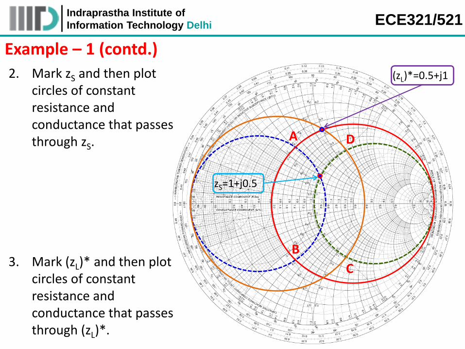
zS=1+j0.5
(zL)*=0.5+j1 2. Mark zS and then plot circles of constant resistance and conductance that passes through zS.
3. Mark (zL)* and then plot circles of constant resistance and conductance that passes through (zL)*.
A
B
D
C

Indraprastha Institute of
Information Technology Delhi ECE321/521
Example – 1 (contd.)
4. The intersection points of these circles are A, B, C and D with the normalized impedances and inductances as:
0.5 0.6Az j 0.8 1Ay j 0.5 0.6Bz j 0.8 1By j
1 1.2Cz j 3 0.5Cy j 1 1.2Dz j 3 0.5Dy j
5. There are four intersection points and therefore four L-type matching circuit configurations are possible.
zS → zA → (zL)* Shunt L, Series L
zS → zB → (zL)* Shunt C, Series L
zS → zC → (zL)* Series C, Shunt L
zS → zD → (zL)* Series L, Shunt L

Indraprastha Institute of
Information Technology Delhi ECE321/521
Example – 1 (contd.) 6. Find the actual values of the components
In the first case:
zS → zA : the normalized admittance is changed by
20.6L A Sjb y y j
2
02 6.63
L
ZL nH
b
zA → zL : the normalized impedance is changed by
1
*
0.4L L Ajx z z j 1 0
1 1.59Lx Z
L nH
Therefore the circuit is:
zS → zA → (zL)*

Indraprastha Institute of
Information Technology Delhi ECE321/521
Example – 1 (contd.)
Similarly:
zS → zB → (zL)* zS → zC → (zL)*
zS → zD → (zL)*
Indraprastha Institute of
Information Technology Delhi ECE321/521
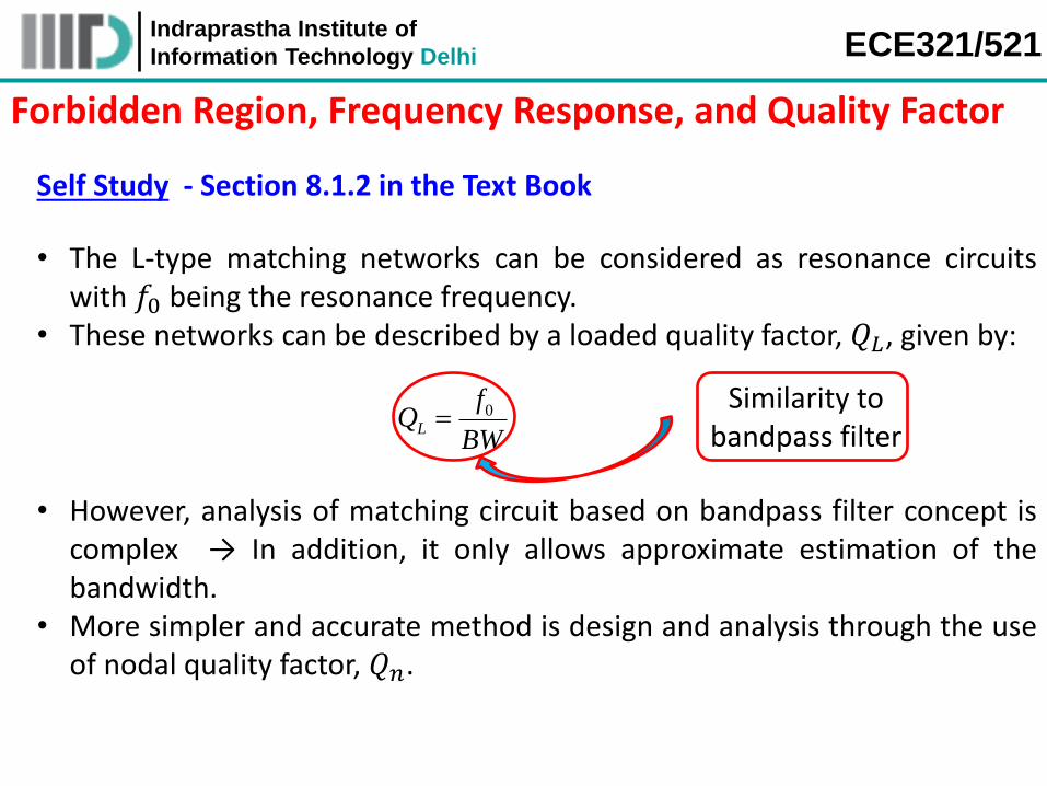
Forbidden Region, Frequency Response, and Quality Factor
Self Study - Section 8.1.2 in the Text Book
• The L-type matching networks can be considered as resonance circuits with 𝑓0 being the resonance frequency.
• These networks can be described by a loaded quality factor, 𝑄𝐿, given by:
0L
fQ
BW
Similarity to bandpass filter
• However, analysis of matching circuit based on bandpass filter concept is complex → In addition, it only allows approximate estimation of the bandwidth.
• More simpler and accurate method is design and analysis through the use of nodal quality factor, 𝑄𝑛.

Indraprastha Institute of
Information Technology Delhi ECE321/521
Nodal Quality Factor
• During L-type matching network analysis it was apparent that at each node the impedance can be expressed in terms of equivalent series impedance 𝑍𝑠 = 𝑅𝑠 + 𝑗𝑋𝑠 or admittance 𝑌𝑃 = 𝐺𝑃 + 𝑗𝐵𝑃 .
S
n
S
XQ
R
• Similarly,
P
n
P
BQ
G
• The “nodal quality factor” and loaded quality factor are related as:
2
nL
True for any L-type matching network
For more complicated networks, QL = Qn
• Therefore, at each node we can define 𝑄𝑛 as the ratio of the absolute value of reactance 𝑋𝑠 to the corresponding resistance 𝑅𝑠.
• BW of the matching network can be easily estimated once the “nodal quality factor” is known.
Indraprastha Institute of
Information Technology Delhi ECE321/521
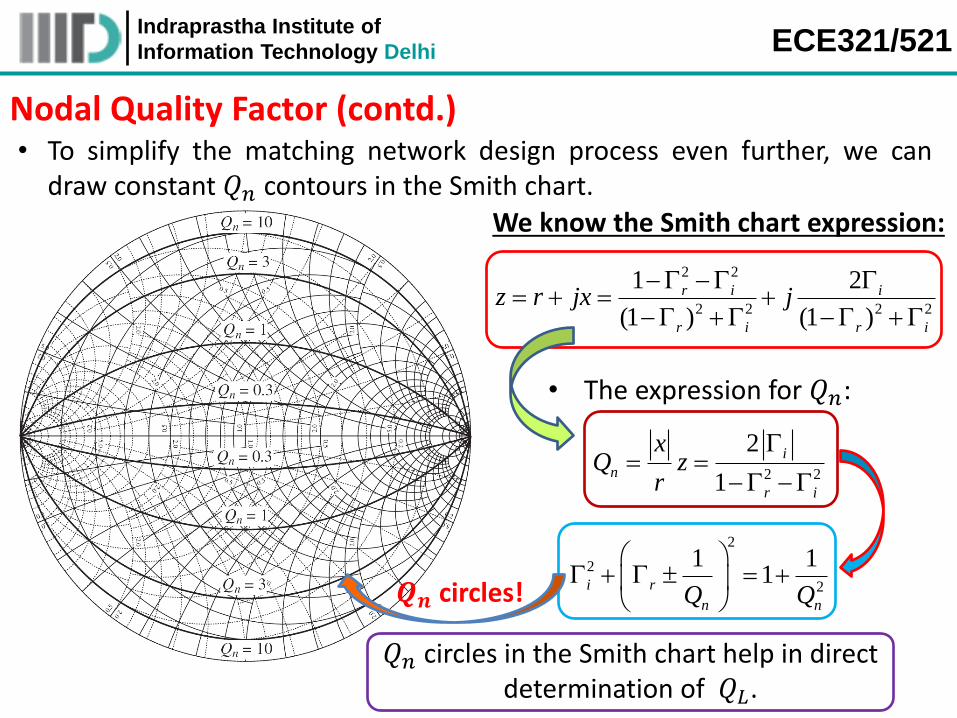
Nodal Quality Factor (contd.) • To simplify the matching network design process even further, we can
draw constant 𝑄𝑛 contours in the Smith chart.
• We know the Smith chart expression:
2 2
2 2 2 2
1 2
(1 ) (1 )
r i i
r i r i
z r jx j
• The expression for 𝑄𝑛:
2 2
2
1
i
n
r i
xQ z
r
2
2
2
1 11i r
n nQ Q
𝑸𝒏 circles!
𝑄𝑛 circles in the Smith chart help in direct determination of 𝑄𝐿.

Indraprastha Institute of
Information Technology Delhi ECE321/521
Nodal Quality Factor (contd.) • Once you go through section 8.1.2, it will be apparent that quality factor of
matching network is extremely important. • For example, broadband amplifier requires matching circuit with low-Q.
Whereas oscillators require high-Q networks to eliminate undesired harmonics in the output signal.
• It will also be apparent that L-type matching networks have no control over the values of 𝑄𝑛 → Limitation!!!
• To gain more freedom in choosing the values of Q or Qn, another element in the matching network is incorporated → results in T- or Pi-network

Indraprastha Institute of
Information Technology Delhi ECE321/521
T- and Pi- Matching Networks • The knowledge of nodal quality factor (𝑄𝑛) of a network enables
estimation of loaded quality factor → hence the Band Width (BW). • The addition of third element into the matching network allows control of 𝑄𝐿 by choosing an appropriate intermediate impedance.
Example – 2 • Design a T-type matching network that transforms a load impedance ZL =
(60 – j30)Ω into a Zin = (10 + j20)Ω input impedance and that has a maximum Qn of 3. Compute the values for the matching network components, assuming that matching is required at f = 1GHz.
Solution • Several possible configurations! Let us focus on just one!

Indraprastha Institute of
Information Technology Delhi ECE321/521
Example – 2 (contd.)
General Topology of a T-matching Network Gives the name T
• First element in series (Z1) is purely reactive, therefore the combined impedance of (ZL and Z1) will reside on the constant resistance circle of r = rL
• Similarly, Z3 (that is purely reactive!) is connected in series with the input, therefore the combined impedance ZB (consisting of ZL, Z1, and Z2) lies on the constant resistance circle r = rin
• Network needs to have a Qn of 3 → we should choose impedance in such a way that ZB is located on the intersection of constant resistance circle r = rin and Qn = 3 circle → helps in the determination of Z3

Indraprastha Institute of
Information Technology Delhi ECE321/521
Example – 2 (contd.)
zL
zin
• The constant resistance circle of zin intersects the 𝑄𝑛 = 3 circle at point B. This gives value of 𝑍3.
• The constant resistance circle 𝑟 = 𝑟𝐿 and a constant conductance circle that passes through B helps in the determination of and allows determination 𝑍2and 𝑍1.
Final solution at 1 GHz

Indraprastha Institute of
Information Technology Delhi ECE321/521
Example – 3 • For a broadband amplifier, it is required to develop a Pi-type matching
network that transforms a load impedance ZL = (10 – j10)Ω into an input impedance of Zin = (20 + j40)Ω. The design should involve the lowest possible Qn. Compute the values for the matching network components, assuming that matching is required at f = 2.4GHz.
• Since the load and source impedances are fixed, we can’t develop a matching network that has Qn lower than the values at locations ZL and Zin
• Therefore in this example, the minimum value of Qn is determined at the input impedance location as Qn = |Xin|/Rin = 40/20 = 2
Solution • Several Configurations possible (including the forbidden!). One such is below:
Z3
Z2
Z1

Indraprastha Institute of
Information Technology Delhi ECE321/521
Example – 3 (contd.)
• In the design, we first plot constant conductance circle g = gin and find its intersection with Qn=2 circle (point B) → determines the value of Z3
• Next find the intersection point (labeled as A) of the g=gL circle and constant-resistance circle that passes through B → determines value of Z2 and Z1
zL
zin
Final solution at 2.4 GHz
Indraprastha Institute of
Information Technology Delhi ECE321/521
Example – 3 (contd.)
• It is important to note that the relative positions of Zin and ZL allows only one optimal Pi-type network for a given specification.
• All other realizations will result in higher Qn → essentially smaller BW! • Furthermore, for smaller ZL the Pi-matching isn’t possible!
It is thus apparent that BW can’t be enhanced arbitrarily by reducing the 𝑄𝑛. The limits are set by the desired complex 𝑍𝑖𝑛 and 𝑍𝐿.
With increasing frequency and correspondingly reduced wavelength the influence of parasitics in the discrete elements are noticeable → distributed matching networks overcome most of the limitations (of
discrete components) at high frequency
Indraprastha Institute of
Information Technology Delhi ECE321/521
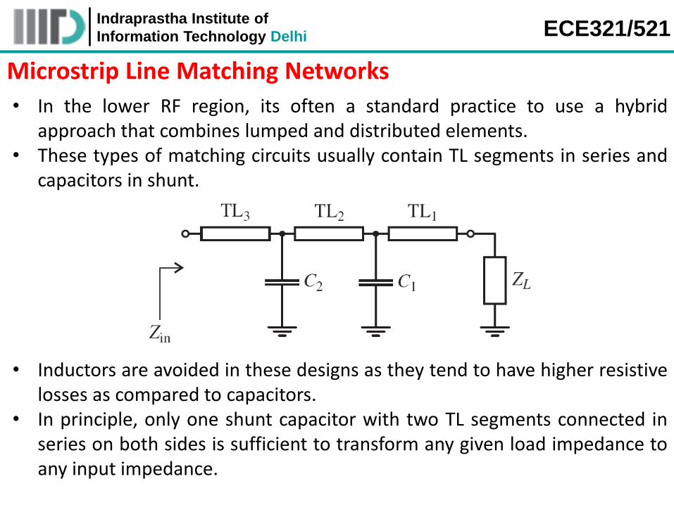
Microstrip Line Matching Networks
• In the lower RF region, its often a standard practice to use a hybrid approach that combines lumped and distributed elements.
• These types of matching circuits usually contain TL segments in series and capacitors in shunt.
• Inductors are avoided in these designs as they tend to have higher resistive losses as compared to capacitors.
• In principle, only one shunt capacitor with two TL segments connected in series on both sides is sufficient to transform any given load impedance to any input impedance.
Indraprastha Institute of
Information Technology Delhi ECE321/521
Microstrip Line Matching Networks (contd.)
• Similar to the L-type matching network, these configurations may also involve the additional requirement of a fixed Qn, necessitating additional components to control the bandwidth of the circuit.
• In practice, these configurations are extremely useful as they permit tuning of the circuits even after manufacturing → changing the values of capacitors as well as placing them at different locations along the TL offers a wide range of flexibility → In general, all the TL segments have the same width to simplify the actual tuning →the tuning ability makes these circuits very appropriate for prototyping.

Indraprastha Institute of
Information Technology Delhi ECE321/521
Example – 4 Design a hybrid matching network that transforms the load ZL = (30 + j10) Ω to an input impedance Zin = (60 + j80) Ω. The matching network should contain only two series TL segments and one shunt capacitor. Both TLs have a 50Ω characteristic impedance, and the frequency at which the matching is required is f = 1.5 GHz
Solution
• Mark the normalized load impedance (0.6 + j0.2) on the Smith chart. • Draw the corresponding SWR circle. • Mark the normalized input impedance (1.2 + j1.6) on the Smith chart. • Draw the corresponding SWR circle. • The choice of the point from which we transition from the load SWR circle
to the input SWR circle can be made arbitrarily.

Indraprastha Institute of
Information Technology Delhi ECE321/521
Example – 4 (contd.) Normalized load
to the point A gives length of
the first segment of TL
point B to normalized input impedance gives
length of the second segment
of TL
A to B provides the necessary susceptance value for the
shunt capacitor


