
LECTURE 12 - ggn.dronacharya.info · >varactor diode-variable capacitance diode P-n Junction ......
42
LECTURE 12 LECTURE 12 -p-n Junction
Transcript of LECTURE 12 - ggn.dronacharya.info · >varactor diode-variable capacitance diode P-n Junction ......

LECTURE 12LECTURE 12
-p-n Junction

Topics to be coveredTopics to be covered P-n Junction
The p-n junction is the basic element of allbipolar devices. Its main electrical property isthat it rectifies (allow current to flow easily in onedirection only).The p-n junction is often justcalled a DIODE. Applications;
>photodiode, light sensitive diode,>LED- ligth emitting diode,>varactor diode-variable capacitance diode
P-n Junction
The p-n junction can be formed by pushing apiece of p-type silicon into close contact with apiecce of n-type silicon. But forming a p-njunction is not so simply. Because;
1) There will only be very few points of contactand any current flow would be restricted tothese few points instead of the whole surfacearea of the junction.
2) Silicon that has been exposed to the air alwayshas a thin oxide coating on its surface calledthe “native oxide”. This oxide is a very goodinsulator and will prevent current flow.
3) Bonding arrangement is interrupted at thesurface; dangling bonds.
The formation of pThe formation of p--n junction :n junction :
To overcome these surface states problems
p-n junction can be formed in the bulk of the semiconductor, away from the
surface as much as possible.
Surface states
EC
Eİ
EV
Ef
EC
Eİ
EV
Ef
EC
Eİ
EV
Ef
p-type n-typeEC
Eİ
EV
Ef
p-type n-type
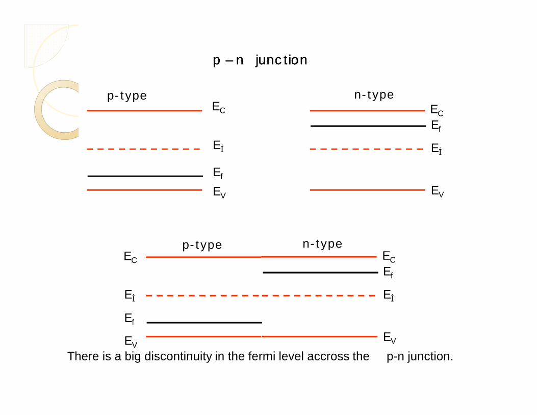
p p –– n junctionn junction
There is a big discontinuity in the fermi level accross the p-n junction.
++++++++++++++++++++++++++++++++++++++++
- - - - -- - - - -- - - - -- - - - -- - - - -- - - - -- - - - -- - - - -
Hole Movement
ElectronMovement
++++++++++++
Fixed positive space-charge
- - - -- - - -- - - -
Fixed negativespace-charge
Ohmic end-contact
n-type p-type
Metallurgical junction
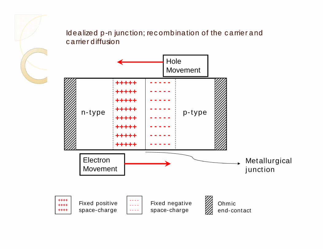
Idealized pIdealized p--n junction; recombination of the carrier and n junction; recombination of the carrier and carrier diffusioncarrier diffusion
Lots of electrons on the left hand side of thejunction want to diffuse to the right and lots ofholes on the right hand side of the junction wantto move to the left.
The donors and acceptors fixed,don’t move(unless you heat up semiconductors, so they candiffuse) because they are elements (such asarsenic and boron) which are incorporated tolattice.
However, the electrons and holes that come fromthem are free to move.
p p –– n junctionn junction
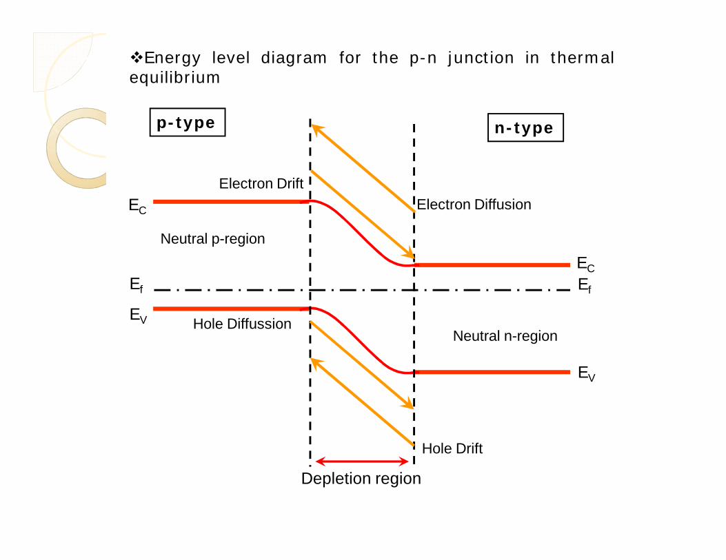
Holes diffuse to the left of the metalurgical junction and combinewith the electrons on that side. They leave behind negativelycharged acceptor centres.
Similarly, electrons diffusing to the right will leave behindpositively charged donor centres. This diffusion process can not goon forever. Because, the increasing amount of fixed charge wantsto electrostatically attract the carriers that are trying to diffuseaway(donor centres want to keep the electrons and acceptorcentres want to keep the holes). Equlibrium is reached.
This fixed charges produce an electric field which slows down thediffusion process.
This fixed charge region is known as depletion region or spacecharge region which is the region the free carriers have left.
It is called as depletion region since it is depleted of free carriers.
Idealized pIdealized p--n junctionn junction
EC
EV
Ef
p-type n-type
EC
EV
Ef
Depletion region
Hole Diffussion
Hole Drift
Electron DiffusionElectron Drift
Neutral p-region
Neutral n-region
Energy level diagram for the p-n junction in thermalequilibrium
2
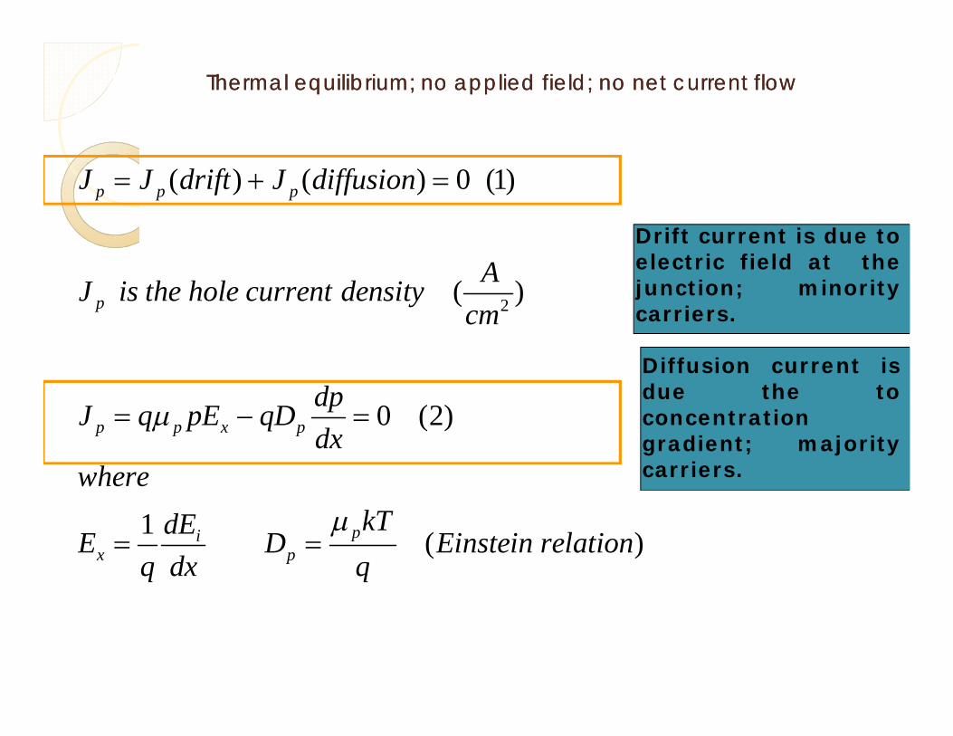
( ) ( ) 0 (1)
( )
0 (2)
1 ( )
p p p
p
p p x p
pix p
J J drift J diffusion
AJ is the hole current densitycm
dpJ q pE qDdx
wherekTdEE D Einstein relation
q dx q
Drift current is due toelectric field at thejunction; minoritycarriers.
Diffusion current isdue the toconcentrationgradient; majoritycarriers.
Thermal equilibrium; no applied field; no net current flowThermal equilibrium; no applied field; no net current flow

( ) 0 ( 3 )
e x p ( ) ( )
0 ( 4 )
0
.
0 (5 )
ip p
i f fii
fp p
f
fn n
d E d pJ p k Td x d x
E E d Ed Ed p pp nk T d x k T d x d x
d EJ p
d x
d Ew e c o n c lu d e th a t w h ic h s ta te s th a t
d xth e F e r m i L e v e l i s a C O N S T A N T a t e q u i l ib r iu m
d EJ n
d x
ProofProof
The drift and diffusion currents are flowing all thetime. But, in thermal equilibrium, the net currentflow is zero since the currents oppose each other.
Under non-equilibrium condition, one of thecurrent flow mechanism is going to dominateover the other, resulting a net current flow.
The electrons that want to diffuse from the n-type layer to the p-layer have potential barier.
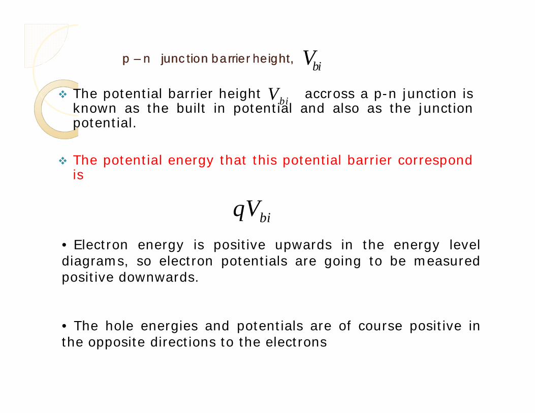
The potential barrier height accross a p-n junction isknown as the built in potential and also as the junctionpotential.
The potential energy that this potential barrier correspondis
biVbiV
biqV• Electron energy is positive upwards in the energy leveldiagrams, so electron potentials are going to be measuredpositive downwards.
• The hole energies and potentials are of course positive inthe opposite directions to the electrons
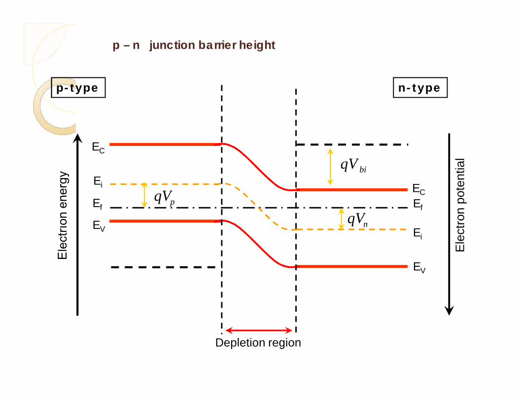
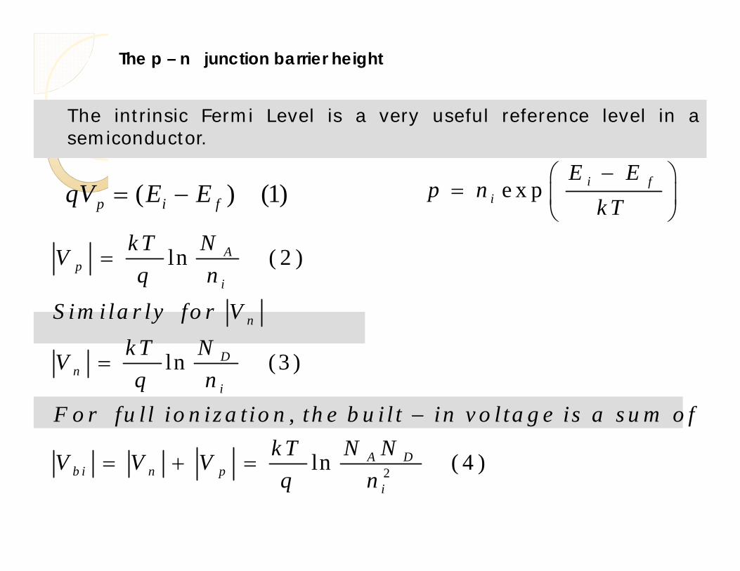
p p –– n junction barrier height,n junction barrier height,
EC
EV
Ef
p-type n-type
EC
EV
Ef
Depletion region
Ei
Ei
biqV
pqV
nqV
Ele
ctrıo
n en
ergy
Ele
ctro
n po
tent
ial
p – n junction barrier height
2
e x p
ln ( 2 )
ln (3 )
,
ln ( 4 )
i fi
Ap
i
n
Dn
i
A Db i n p
i
E Ep n
k Tk T NVq n
S im i la r ly fo r Vk T NVq n
F o r fu l l io n iz a t io n th e b u i l t in v o l ta g e is a s u m o fk T N NV V Vq n
The intrinsic Fermi Level is a very useful reference level in asemiconductor.
( ) (1)p i fqV E E
The p – n junction barrier height
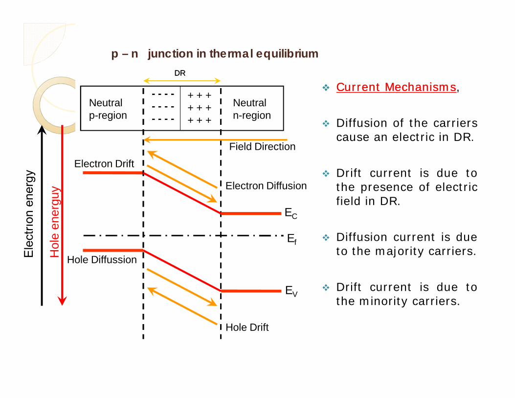
CurrentCurrent MechanismsMechanisms,
Diffusion of the carrierscause an electric in DR.
Drift current is due tothe presence of electricfield in DR.
Diffusion current is dueto the majority carriers.
Drift current is due tothe minority carriers.
Ele
ctrıo
n en
ergy
+ + + + + ++ + +
- - - -- - - -- - - -
Neutral p-region
Neutral n-region
Hole Diffussion
Electron Diffusion
Electron Drift
Hole Drift
Field Direction
Hol
e en
ergu
y
EC
EV
Ef
DRDR
p – n junction in thermal equilibrium
Ele
ctrıo
n en
ergy
+ + + + + ++ + +
- - - -- - - -- - - -
Neutral p-region
Neutral n-region
Hole Diffussion
Electron Diffusion
Electron Drift
Hole Drift
Field Direction
Hol
e en
ergu
y
EC
EV
Ef
DRDR
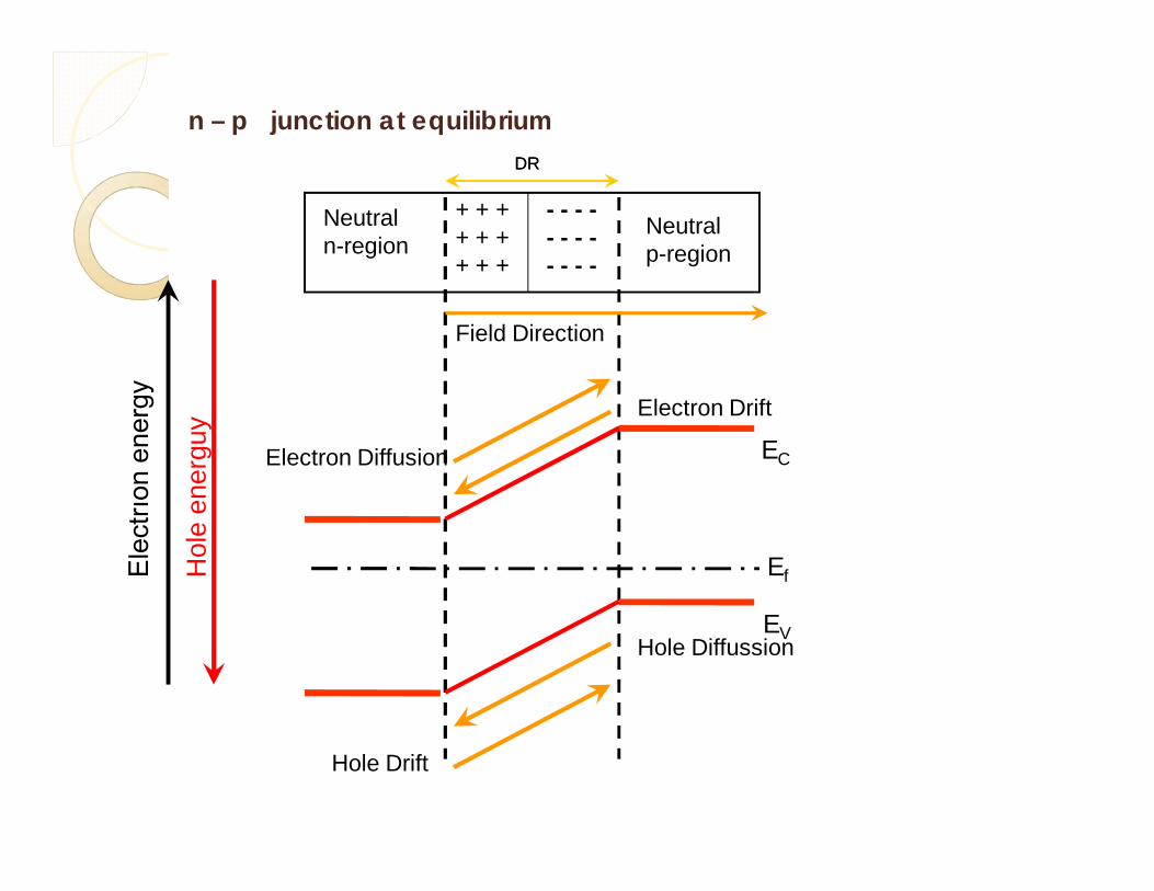
n – p junction at equilibrium
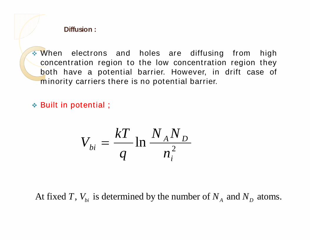
When electrons and holes are diffusing from highconcentration region to the low concentration region theyboth have a potential barrier. However, in drift case ofminority carriers there is no potential barrier.
BuiltBuilt inin potentialpotential ;;
2lni
DAbi n
NNq
kTV
At fixed , is determined by the number of and atoms.bi A DT V N N
Diffusion :

+ + ++ + +
- - - -- - - -p-type n-type
Pote
ntia
l E
lect
ric
field
C
harg
e de
nsity
+ + ++ + +
- - - -- - - -
biV area
mE
biqVxx
xx
xx
Depletion Region
At equilibrium, there is nobias, i.e. no appliedvoltage.
The field takes the samesign as the charge
The sign of the electric fieldis opposite to that of thepotential ;
nv
dVEdx
nx px
Depletion Approximation, Electric Field and Potential for pn junction
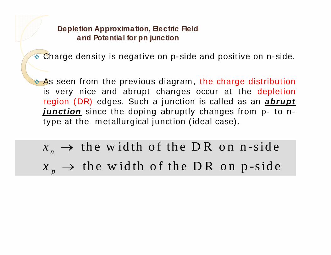
Charge density is negative on p-side and positive on n-side.
As seen from the previous diagram, the charge distributionis very nice and abrupt changes occur at the depletionregion (DR) edges. Such a junction is called as an abruptjunction since the doping abruptly changes from p- to n-type at the metallurgical junction (ideal case).
th e w id th o f th e D R o n n -s id eth e w id th o f th e D R o n p -s id e
n
p
xx
Depletion Approximation, Electric Field and Potential for pn junction

In reality, the charge distribution tails-off into theneutral regions, i.e. the charge distrubition is notabrupt if one goes from depletion region into theneutral region. This region is called as atransition region and since the transition regionis very thin, one can ignore the tail-off regionand consider the change being abrupt. So thisapproximation is called as DEPLETIONAPPROXIMATION.
Depletion Approximation, Electric Field and Potential for pn junction
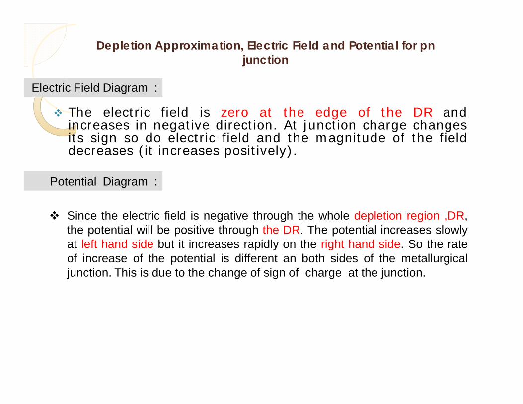
The electric field is zero at the edge of the DR andincreases in negative direction. At junction charge changesits sign so do electric field and the magnitude of the fielddecreases (it increases positively).
Electric Field Diagram :
Potential Diagram :
Since the electric field is negative through the whole depletion region ,DR,the potential will be positive through the DR. The potential increases slowlyat left hand side but it increases rapidly on the right hand side. So the rateof increase of the potential is different an both sides of the metallurgicaljunction. This is due to the change of sign of charge at the junction.
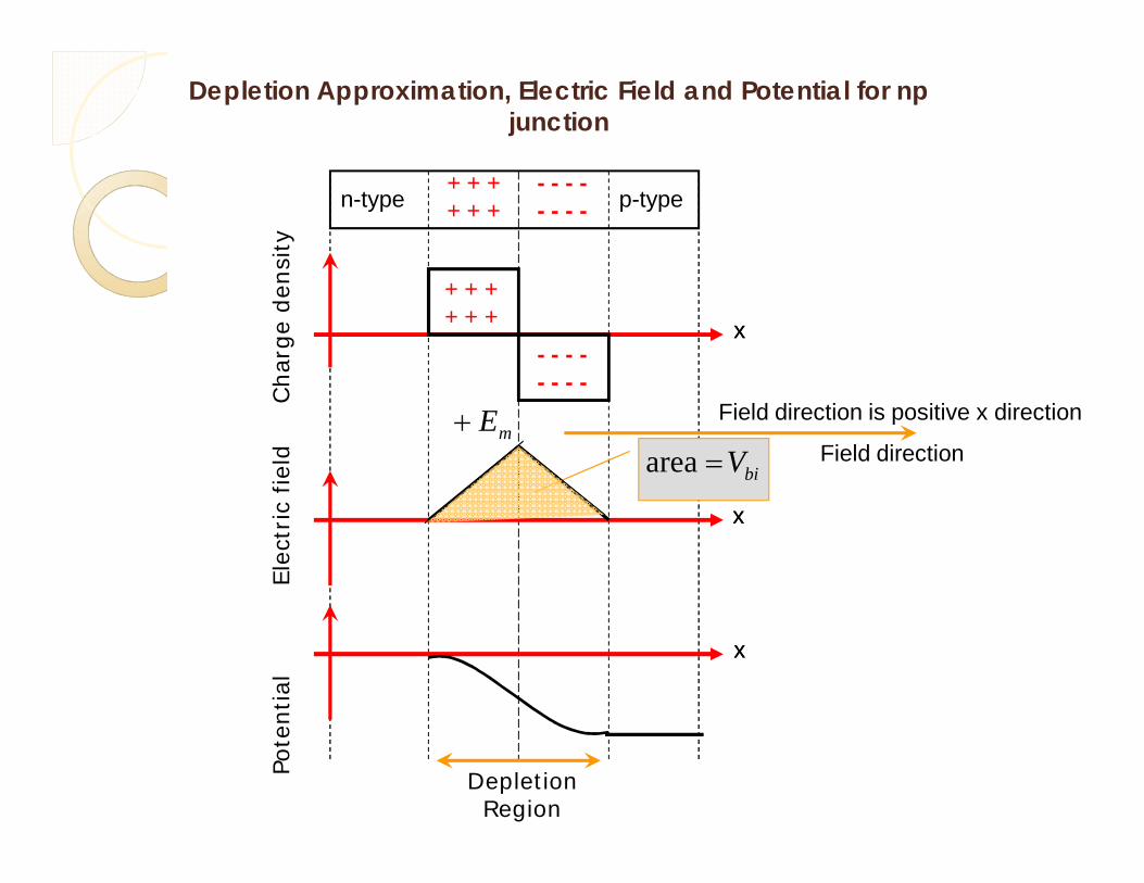
Depletion Approximation, Electric Field and Potential for pn junction
+ + ++ + +
- - - -- - - - p-typen-type
+ + ++ + +
- - - -- - - -
biV area mE
xx
xx
xx
Depletion Region
Field direction is positive x direction
Field direction
Pote
ntia
l E
lect
ric
field
C
harg
e de
nsity
Depletion Approximation, Electric Field and Potential for np junction
+ + ++ + +
- - - -- - - -p-type n-type
Cha
rge
dens
ity + + ++ + +
- - - -- - - -
xx
Depletion Region
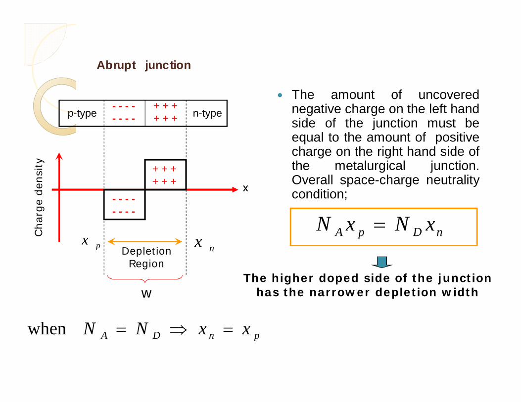
pxnx
The amount of uncoverednegative charge on the left handside of the junction must beequal to the amount of positivecharge on the right hand side ofthe metalurgical junction.Overall space-charge neutralitycondition;
A p D nN x N x
w
pnDA xxNN when
The higher doped side of the junction has the narrower depletion width
Abrupt junction
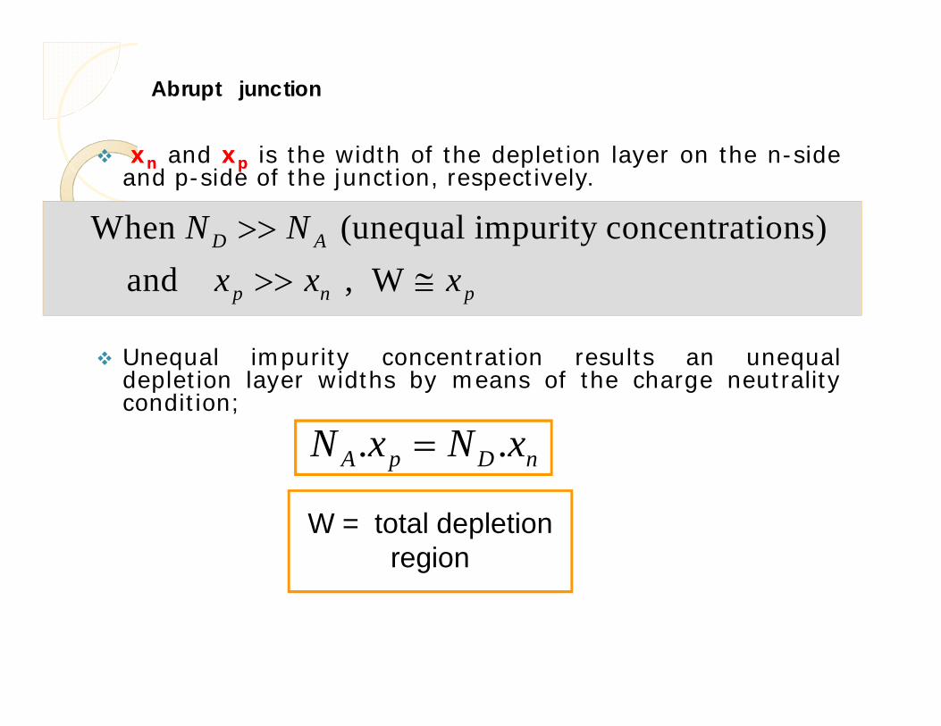
xxnn and xxpp is the width of the depletion layer on the n-sideand p-side of the junction, respectively.
Unequal impurity concentration results an unequaldepletion layer widths by means of the charge neutralitycondition;
nDpA xNxN ..
W = total depletion region
When (unequal impurity concentrations) and , W
D A
p n p
N Nx x x
Abrupt junction
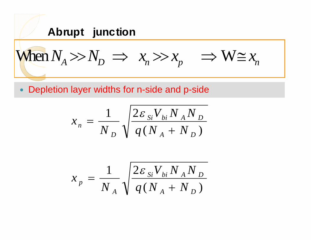
When WA D n p nN N x x x
Depletion layer widths for n-side and p-side
)(21
)(21
DA
DAbiSi
Ap
DA
DAbiSi
Dn
NNqNNV
Nx
NNqNNV
Nx
Abrupt junction

p n
+ -
forward bias
p n
- +
reverse bias
How current flows through the p-njunction when a bias (voltage) isapplied.
The current flows all the timewhenever a voltage source isconnected to the diode. But the currentflows rapidly in forward bias, howevera very small constant current flows inreverse bias case.
Appliying bias to p-n junction
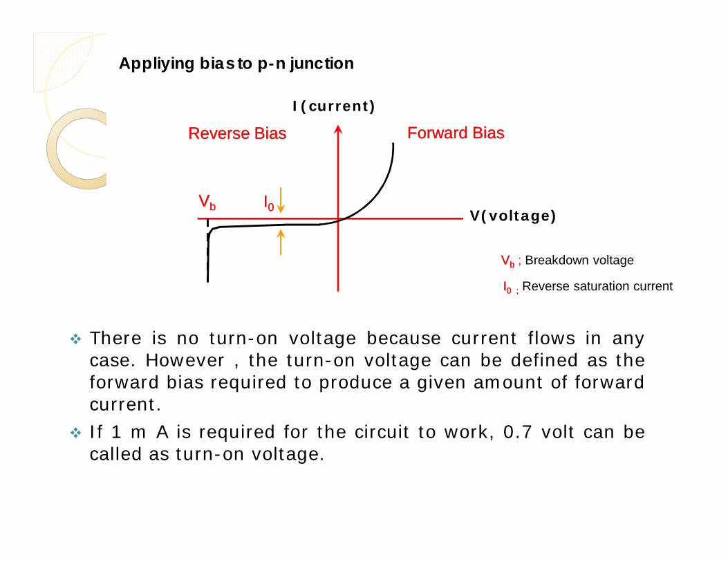
There is no turn-on voltage because current flows in anycase. However , the turn-on voltage can be defined as theforward bias required to produce a given amount of forwardcurrent.
If 1 m A is required for the circuit to work, 0.7 volt can becalled as turn-on voltage.
VVbb II00
VVbb ; Breakdown voltage
II0 ;0 ; Reverse saturation current
Forward BiasForward BiasReverse BiasReverse Bias
I(current)
V(voltage)
Appliying bias to p-n junction
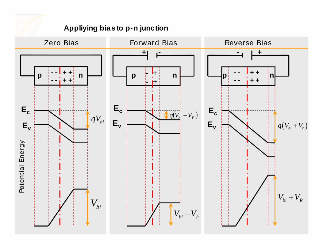
+ - - +
p n p n p n
biqV
biV
Fbi VVq
Fbi VV
bi rq V V
Rbi VV
+ + + +
- -- -
++
--
+ + + +
- -- -
Pote
ntia
l Ene
rgy
Zero Bias Forward Bias Reverse Bias
Ec
EvEv Ev
Ec Ec
Appliying bias to p-n junction
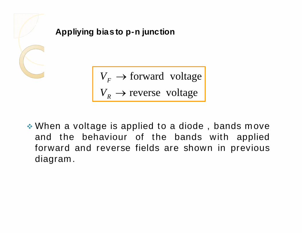
When a voltage is applied to a diode , bands moveand the behaviour of the bands with appliedforward and reverse fields are shown in previousdiagram.
voltagereverse voltageforward
R
F
VV
Appliying bias to p-n junction
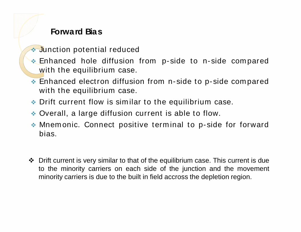
Junction potential reduced Enhanced hole diffusion from p-side to n-side compared
with the equilibrium case. Enhanced electron diffusion from n-side to p-side compared
with the equilibrium case. Drift current flow is similar to the equilibrium case. Overall, a large diffusion current is able to flow. Mnemonic. Connect positive terminal to p-side for forward
bias.
Drift current is very similar to that of the equilibrium case. This current is dueto the minority carriers on each side of the junction and the movementminority carriers is due to the built in field accross the depletion region.
Forward Bias
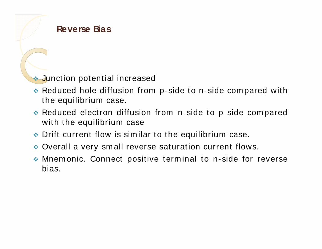
Junction potential increased Reduced hole diffusion from p-side to n-side compared with
the equilibrium case. Reduced electron diffusion from n-side to p-side compared
with the equilibrium case Drift current flow is similar to the equilibrium case. Overall a very small reverse saturation current flows. Mnemonic. Connect positive terminal to n-side for reverse
bias.
Reverse Bias
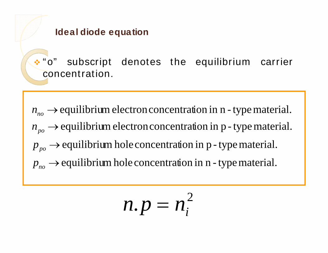
“o” subscript denotes the equilibrium carrierconcentration.
material. type-nin ion concentrat hole mequilibriumaterial. type-pin ion concentrat hole mequilibriu
material. type-pin ion concentratelectron mequilibriumaterial. type-nin ion concentratelectron mequilibriu
no
po
po
no
ppnn
2. inpn
Ideal diode equation
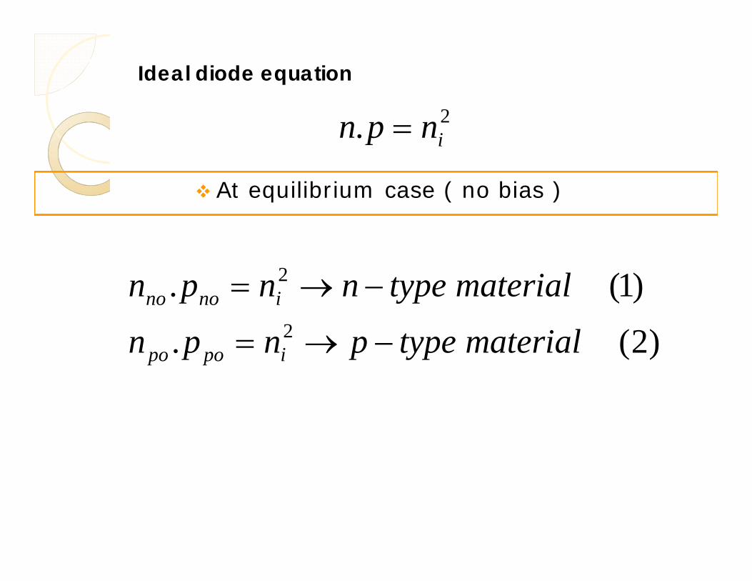
At equilibrium case ( no bias )
)2(.
)1(.
.
2
2
2
materialtypepnpnmaterialtypennpn
npn
ipopo
inono
i
Ideal diode equation
2
22
ln assuming full ionization
; majority carriers
.ln . for n-type
ln exp (3)
A Dbi
i
A po D no
po nobi no no i
i
po bibi po no
no
kT N NVq n
N p N n
p nkTV n p nq n
p qVkTV p pq p kT
Ideal diode equation
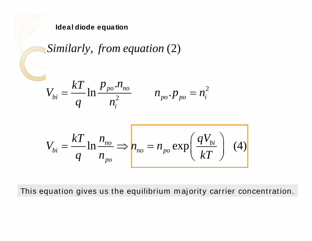
22
, (2)
.ln .
ln exp (4)
po nobi po po i
i
no bibi no po
po
Similarly from equation
p nkTV n p nq n
n qVkTV n nq n kT
This equation gives us the equilibrium majority carrier concentration.
Ideal diode equation
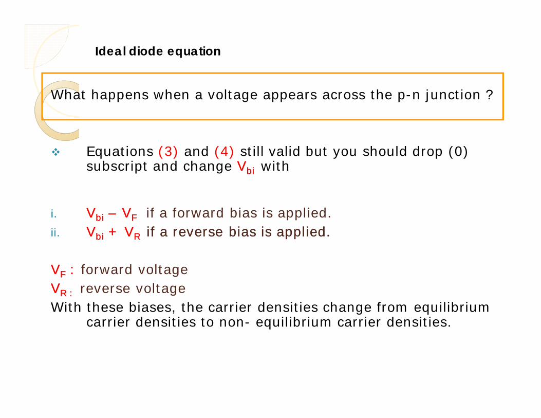
What happens when a voltage appears across the p-n junction ?
Equations (3) and (4) still valid but you should drop (0) subscript and change VVbi bi with
i.i. VVbibi –– VVF F if a forward bias is applied.ii.ii. VVbibi + V+ VR R if a reverse bias is applied.if a reverse bias is applied.
VVFF : : forward voltageVVR :R : reverse voltageWith these biases, the carrier densities change from equilibrium
carrier densities to non- equilibrium carrier densities.
Ideal diode equation

Non-equilibrium majority carrier concentration in forward bias;
( )e x p
F o r e x a m p le ; f o r r e v e r s e b i a s
( )e x p
b i Fp n
n
b i Rn p
q V Vp pk T
n
q V Vn nk T
• When a voltage is applied; the equilibrium nno changes to the non equilibrium nn.
Ideal diode equation
An applied reverse bias (voltage) will result in a smallcurrent to flow through the device.
At a particular high voltage value, which is called asbreakdown voltage VB, large currents start to flow. If thereis no current limiting resistor which is connected in seriesto the diode, the diode will be destroyed. There are twophysical effects which cause this breakdown.
1)1) ZenerZener breakdownbreakdown is observed in highly doped p-n junctions and occursfor voltages of about 5 V or less.
2)2) AvalancheAvalanche breakdownbreakdown is observed in less highly doped p-n junctions.
Junction breakdown or reverse breakdown
Zener breakdown occurs at highly doped p-njunctions with a tunneling mechanism.
In a highly doped p-n junction the conductionand valance bands on opposite side of thejunction become so close during the reverse-biasthat the electrons on the p-side can tunnel fromdirectly VB into the CB on the n-side.
Zener breakdown
Avalanche breakdown mechanism occurs whenelectrons and holes moving through the DR andacquire sufficient energy from the electric fieldto break a bond i.e. create electron-hole pairsby colliding with atomic electrons within thedepletion region.
The newly created electrons and holes move inopposite directions due to the electric field andthereby add to the existing reverse bias current.This is the most important breakdownmechanism in p-n junction.


![Chapter 1: Diode circuits vtusolutionvtusolution.in/uploads/9/9/9/3/99939970/analog_electronic[15ec32].pdf · Chapter 1: Diode circuits ... • Diode testing • Zener diode • Diode](https://static.fdocuments.in/doc/165x107/5aedefea7f8b9a9031905d54/chapter-1-diode-circuits-vt-15ec32pdfchapter-1-diode-circuits-diode.jpg)


