LECTRONIC AND OPTICAL PROPERTIES OF … ELECTRONIC AND OPTICAL PROPERTIES OF NANOMATERIALS 1.1...
42
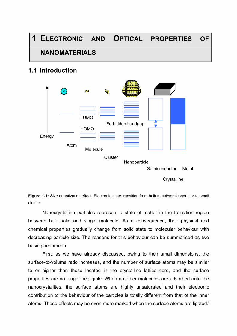
1 ELECTRONIC AND OPTICAL PROPERTIES OF NANOMATERIALS 1.1 Introduction Figure 1-1: Size quantization effect. Electronic state transition from bulk metal/semiconductor to small cluster. Nanocrystalline particles represent a state of matter in the transition region between bulk solid and single molecule. As a consequence, their physical and chemical properties gradually change from solid state to molecular behaviour with decreasing particle size. The reasons for this behaviour can be summarised as two basic phenomena: First, as we have already discussed, owing to their small dimensions, the surface-to-volume ratio increases, and the number of surface atoms may be similar to or higher than those located in the crystalline lattice core, and the surface properties are no longer negligible. When no other molecules are adsorbed onto the nanocrystallites, the surface atoms are highly unsaturated and their electronic contribution to the behaviour of the particles is totally different from that of the inner atoms. These effects may be even more marked when the surface atoms are ligated. i Energy Forbidden bandgap HOMO LUMO Molecule Nanoparticle Semiconductor Metal Crystalline Atom Cluster
Transcript of LECTRONIC AND OPTICAL PROPERTIES OF … ELECTRONIC AND OPTICAL PROPERTIES OF NANOMATERIALS 1.1...
1 ELECTRONIC AND OPTICAL PROPERTIES OF
NANOMATERIALS
1.1 Introduction
Figure 1-1: Size quantization effect. Electronic state transition from bulk metal/semiconductor to small
cluster.
Nanocrystalline particles represent a state of matter in the transition region
between bulk solid and single molecule. As a consequence, their physical and
chemical properties gradually change from solid state to molecular behaviour with
decreasing particle size. The reasons for this behaviour can be summarised as two
basic phenomena:
First, as we have already discussed, owing to their small dimensions, the
surface-to-volume ratio increases, and the number of surface atoms may be similar
to or higher than those located in the crystalline lattice core, and the surface
properties are no longer negligible. When no other molecules are adsorbed onto the
nanocrystallites, the surface atoms are highly unsaturated and their electronic
contribution to the behaviour of the particles is totally different from that of the inner
atoms. These effects may be even more marked when the surface atoms are ligated.i
Energy
Forbidden bandgap HOMO
LUMO
Molecule
NanoparticleSemiconductor Metal
Crystalline
Atom
Cluster
This leads to different electronic transport and catalytic properties of the
nanocrystalline particles.ii
The second phenomenon, which occurs in metal and semiconductor
nanoparticles, is totally an electronic effect. The band structure gradually evolves with
increasing particle size, i. e., molecular orbital convert into delocalised band states.
Figure 1-1, shows the size quantization effect responsible for the transition between
a bulk metal or semiconductor, and cluster species. In a metal, the quasi-continuous
density of states in the valence and the conduction bands splits into discrete
electronic levels, the spacing between these levels and the band gap increasing with
decreasing particle size.iii,iv
In the case of semiconductors, the phenomenon is slightly different, since a
band gap already exists in the bulk state. However, this band gap also increases
when the particle size is decreased and the energy bands gradually convert into
discrete molecular electronic levels.v If the particle size is less than the De Broglie
wavelength of the electrons, the charge carriers may be treated quantum
mechanically as "particles in a box", where the size of the box is given by the
dimensions of the crystallites. vi In semiconductors, the quantization effect that
enhances the optical gap is routinely observed for clusters ranging from 1 nm to
almost 10 nm. Metal particles consisting of 50 to 100 atoms with a diameter between
1 and 2 nm start to loose their metallic behaviour and tend to become
semiconductors.vii Particles that show this size quantization effect are sometimes
called Q-particles or quantum dots that we will discuss later in this chapter.
At very small particle sizes, also called clusters, determined by the so-called
magic numbers, which are more frequently observed than others. Metals have a
cubic or hexagonal close-packed structure consisting of one central atom, which is
surrounded in the first shell by 12 atoms, in the second shell by 42 atoms, or in
principle by 10n2+2 atoms in the nth shell.viii For example, one of the most famous
ligand stabilized metal clusters is a gold particle with 55 atoms (Au55) first reported by
G. Schmid in 1981.ix
1.2 Metals
1.2.1 Introduction
Nanowires and nanocrystals having average radius R, in the range of the Fermi
wavelength λF, can indeed be fabricated and have shown unusual mechanical and
electronic properties. The effects of reduced size and dimensionality, and their
quantum properties have been investigated actively in the last decade. Ultrathin
nanowires and even monatomic chains suspended between two metal electrodes
have been produced. Electrical conduction and force have been measured
concomitantly in the course of stretching of nanowires. Initially, much of the work was
carried out on GaAs–AlGaAs heterostructures which were grown to contain a thin
conducting layer at the interface. The conducting layer is treated as a two-
dimensional (2D) electron gas in which a narrow constriction of desired width w, and
length l, can be created by applying a negative gate voltage.
The conductivity σ, which relates the electric current density to the electric field by
j = σE, is expressible in terms of the areal charge density ρS for 2D electron gas of
effective mass m∗ through the equation
*
2
meS τρ
σ = (1. 1)
The experimental quantity of interest, however, is the conductance G = I /V, which is
the ratio of the total current I to the voltage drop V across the sample of length l in the
direction of current flow. For 2D, since I = wj, one can also write
lwG σ= (1. 2)
For a 3D conductor, this relationship is valid provided that w is replaced by the cross
sectional area A orthogonal to the current flow direction. Similar expressions are also
valid for the thermal transport of energy. The thermal conductance related to the
energy (or heat) current Jx through a sample between two reservoirs is given by
kx = Jx ∆T , where ∆T is the temperaturegradient. Depending on whether the energy
is carried by electrons (x = e) or by phonons (x = p) the thermal conductance is
identified as electronic Ke or phononic Kp. Here our focus is on quantum transport
through materials of very small dimensions.
Novel size-dependent effects emerge as w and l are reduced towards nanometric
dimensions in the nanometre range. The relationship expressed by equation lwG σ=
(1. 2) holds in the diffusive transport regime where both w and l are greater
than the mean free path. As the width of the constriction decreases, there comes a
point where quantum mechanics makes its presence known. The quantum
confinement of a carrier in a strip of width w leads to the discretization of energy
levels given by
єn = n2h2/(8m∗w2). The number of these w-dependent transverse modes, which are
occupied, determines the conductance. Thus, rather than a simple linear
dependence of G on w, quantum mechanics forces this ‘indirect’ dependence on w.
As w is altered, the energy spectrum changes and so does the number of occupied
modes below the Fermi energy and hence the conductance.
Simple physical considerations show that the number of transverse occupied states,
N ∼ 2w/λF, increases with the width of the constriction. Since all these modes can
contribute to the conductance, one still expects the conductance to increase linearly
with w even in the nanodomain. This is almost the case, except with one important
distinction. The width w can change continuously, at least in principle. But the
number of modes, being an integer, can only vary in discrete steps. The concept
becomes physically more transparent if we rewrite ~ F
n
EN nε
. The highest occupied
εn = EF gives N from a simple counting of the number of discrete eigenvalues. Since it
is a rare coincidence for an eigenvalue to exactly align with the Fermi energy, N is
taken to be the integer which corresponds to the highest occupied level just below
EF. Thus the effect of quantum mechanics due to the reduced dimension w is to
cause the conductance to change in discrete steps in a staircase fashion. We have
yet to find the step height. This simple view is necessarily modified when other
factors explained later start to play a crucial role. Obviously, one then requires a
more detailed analysis.
The characteristic length that comes into play is λF, since only those electrons having
energy close to the Fermi energy carry current at low temperatures. If w >> λF, the

number of conducting modes is very large and so is the conductance. This is typical
in metals where λF ∼ 0.2 nanometres is very small and consequently the observation
of discrete conductance variation requires w ∼ λF. That is why the discrete
conductance behaviour was first observed in semiconductor heterojunctions having
very low electron density and λF two orders of magnitude larger than in metals.
The effect of reduced length l on the conductance is even more striking. If the ohmic
regime were to hold in equation lwG σ=
(1. 2), one would expect G to increase
without limit (or resistance to reach zero) as l was reduced towards zero. We shall
see that there would always be finite residual resistance. Heisenberg’s uncertainty
principle defines a natural characteristic length as the mean free path le. If l < le,
carriers can propagate without losing their initial momentum, and this domain is
referred to as the ballistic transport regime. If we follow the standard definition, that
the conductance is a measure of current through a sample divided by the voltage
difference,
VG
ΔΙ
= (1. 3)
the quantum of electrical conductance occurs naturally as a consequence of
Heisenberg’s uncertainty principle. The current is given by the rate of charge flow
I = ∆Q/ttransit . Now charge is quantized in units of elementary charge, e. Hence in the
extreme quantum limit, setting ∆Q = e and recognizing that the transit time should
then be at least in the range of time implied by Heisenberg’s uncertainty principle, we
get
teΔ
=Ι (1. 4)
Combining equation VG
ΔΙ
= (1. 3) and equation t
eΔ
=Ι (1. 4), and using the fact
that the potential difference, ∆V, is equal to electrochemical potential difference ∆E
divided by the electronic charge e, one gets
tEeGΔΔ
=² (1. 5)
Next invoking Heisenberg’s uncertainty principle, ∆E ∆t >> h, the expression for
ballistic conductance including the spin degeneracy becomes G = 2e2/h in the ideal
case. It has a maximum value of 8×10⁻⁵ Ω−1. This is the step height, the conductance
per transverse mode.
The corresponding resistance h/2e2 has a value of 12.9 kΩ (it suffices to call it
12345Ω for ease of remembrance) and is attributed to the resistance at the contacts
where the conductor is attached to the electrodes or electron reservoirs. Thus
classically G ∝ w. Quantum mechanically it increases in discrete steps. It jumps by
2e2/h as w increases enough to permit one more transverse mode to be occupied
and hence available for conduction. More recently, the electronic and transport
properties of metallic point contacts and wires having average dimension in the range
of metallic λF produced by STM and also by mechanical break junctions have
displayed various quantum effects. The two-terminal electrical conductance, G, of the
wire showed a stepwise variation with the stretch.
Quantum transport of electrons In 1957, Landauer introduced a novel way of looking at conduction. He taught us to
view the conduction as transmission and gave the famous formula, which has been a
breakthrough in the conductance phenomena and in the physics of mesoscopic
systems. According to Landauer, the conduction is a scattering event, and the
transport is the consequence of the incident current flux. On the basis of the self-
consistency arguments for reflections (R) and transmissions (T), he derived his
famous formula for a one-dimensional conductor yielding the conductance
G = (2e²/h)Τ /R (1. 6)
Where T and R = 1 − T are transmission and reflection coefficients, respectively.
Later, Sharvin investigated the electron transport through a small contact between
two free-electron metals. Since the length of the contact is negligible, i.e. l → 0, the
scattering in the contact was absent and hence T ∼ 1. By using a semiclassical
approach he found an expression for the conductance,
GS = (2e2/h)(Ak2F /4π) (1. 7)
Which has come to be known as Sharvin’s conductance (A =area).
The original Landauer formula, i.e. equation G = (2e²/h)Τ /R (1. 6), and
Sharvin’s conductance have seemed to be at variance, since the former yields G →
∞ as R → 0 in the absence of scattering. The confusion in the literature has been
clarified by recognizing the fact that the original formula is just the conductance of a
barrier in a 1D conductor. Engquist and Anderson pointed out an interesting feature
by arguing that the conductance has a close relation with the type of measurement.
Landauer’s formula was extended to the conductance measured between the two
outside reservoirs within which the finite-length conductor is placed. The
corresponding two-terminal conductance formula, G = (2e2/h)T , incorporates the
resistance due to the contacts to the reservoirs. Accordingly, for perfect transmission,
T ∼ 1, the conductance is still finite and equal to 2e2/h.
The step behaviour of G has been treated in several studies. Here we provide a
simple and formal explanation by using a 1D idealized uniform constriction having a
width w. The electrons are confined in the transverse direction and have states with
quantized energy єi . They propagate freely along the length of the constriction. The
propagation constant γιfor an electron with єi < EF is
( )1/22 *
²i F im Eγ ε⎡ ⎤= −⎢ ⎥⎣ ⎦
(1. 8)
Whenever the width of the constriction increases by λF /2, a new subband with
energy єi + ћ²γ²i/2m dips below the Fermi level and contributes to the current under
the small bias voltage ∆V. The current is
( ) ( )[ ]∑=
−Δ+=Ιj
iFiFii EDVeEDen
i1
2 γϑ (1. 9)
Here j is the index of the highest subband that lies below the Fermi level, i.e.
єi ≤ EF + e∆V and єj+1 > EF + e∆V, and ni is the degeneracy of the state i. By
assuming perfect transmission in the absence of any contact resistance and barrier
inside the constriction, i.e. T = 1, and by expressing the group velocity iγ
ϑ and the
density of states Di (є) in terms of the subband energy є = єi + ћ²γ²i/2m* and dividing I
by ∆V we obtain
∑=
=j
iin
heG
1
²2 (1. 10)
Accordingly, each current-transporting state with energy in the range
EF < є < EF + e∆V contributes to G an amount 2e²ni/h.
For a uniform, infinite wall constriction, the states are non-degenerate, i.e. ni = 1, and
hence the increase of w by λF /2 causes G to jump by 2e²/h. As a result, the G(w)
curve exhibits a staircase structure. Since the level spacing in the transverse
quantization is rather small for the low electron density in the 2D electron gas system,
and ∆є ∼ λF-2, the sharp step structure is likely to be smeared out at T ∼ 10 K or at
finite bias voltage.
For a finite-length constriction the scattering at the contacts to the reservoirs (i.e. the
contact resistance) and at the non-uniformities or the potential barriers inside the
constriction affect the transmission. Then, the conductance of a single channel
expressed as
G = (2e²/h)T (1. 11)
may deviate from the perfect quantized values. As a result, the effects, such as the
contact and potential barrier, surface roughness, impurity scattering, cause the sharp
step structure of G(w) to smear out. The local widening of the constriction or impurity
potential can give rise to quasi-bound (0D) states in the constriction and to resonant
tunnelling effects.
The length of the constriction, l, is another important parameter. In order to get sharp
step structure, l has to be greater than λF , but smaller than the electron mean free
path le; G(w) is smoothed out in a short constriction (l < λF ). Therefore, G(w) exhibits
sharp step structure if the constriction is uniform, and w ∼λF and λF << l < le. On the
other hand, the theoretical studies predict that the resonance structures occur on the
flat plateaus due to the interference of waves reflected from the abrupt connections
to the reservoirs. The stepwise variation of G with w or EF has been identified as the
quantization of conductance. This is, in fact, the reflection of the quantized
constriction states in the electrical conductance.
We now extend the above discussion to analyse the ballistic electron conductance
through a point contact or a nanowire, in which the electronic motion is confined in
two dimensions, but freely propagates in the third dimension. The point contact (or
quantum contact) created by the indentation of the STM, a nanowire (or a connective
neck) that is produced by retracting the tip from an indentation and also a metallic
SWNT are typical systems of interest. Nanowires created by STM are expected to be
round (though not perfectly cylindrical) and have radius R ∼λF at the neck. The neck
is connected to the electrodes by horn-like ends, and hence the radius increases as
one goes away from the neck. An extreme case for l → 0 is Sharvin’s conductance,
GS = (2e²/h)(πR/ λF )², with contact radius R, where the step structure is almost
smeared out and plateaus disappear. In the quantum regime, where the cross
section A ∼λF², GS should vanish when A is smaller than a critical cross section set by
the uncertainty principle. As l increases, a stepwise behaviour for GS develops.
1.2.2 Electrical Conductivity
An atomic size contact and connective neck first created by Gimzewski andMöller by
using a STM tip exhibited abrupt changes in the variation of the conductance with the
displacement of the tip. Initially, the observed behaviour of the conductance was
attributed to the quantization of conductance. At that time, from calculating the
quantized conductance of a perfect but short connective neck, Ciraci and Tekman
concluded that the observed abrupt changes of the conductance can be related to
the discontinuous variation of the contact area. Later, Todorov and Sutton performed
an atomic scale simulation of indentation based on the classical molecular dynamics
(MD) method and calculated the conductance for the resulting atomic structure using
the s-orbital tight-binding Green’s function method. They showed that sudden
changes of conductance during indentation or stretching are related to the
discontinuous variation of the contact area. Recently, nanowires of better quality
have been produced using STM and also by using the mechanical break junction.
The two-terminal electrical conductance of these wires showed abrupt changes with
the stretching.
The radius of the narrowest cross section of the wire prior to the break is only a few
ångströms; it has the length scale of λF , where the discontinuous (discrete) nature of
the metal dominates over its continuum description. Since the level spacing ∆є is in
the region of ∼1 eV at this length scale, the peaks of the density of states D(є) of the
connective neck become well separated and hence the transverse quantization of
states becomes easily resolved even at room temperature. Furthermore, any change
in the atomic structure or the radius induces significant changes in the level spacing
and in the occupancy of states. This, in turn, leads to detectable changes in the
related properties. Therefore, the ballistic electron transport through a nanowire
should be closely related to its atomic structure and radius at its narrowest part. On
the other hand, irregularities of the atomic structure and electronic potential enhance
scattering that destroys the regular staircase structure. In the following section, we
summarize results that emerged from recent experimental and theoretical studies on
stretched nanowires.
1.2.2.1 Atomic structure and mechanical properties
Computer simulations of the atomic structure of connective necks created by STM
were first performed in the seminal works by Sutton and Pethica [], and Landman et
al []. The deformation (or elongation) generally occurred in two different and
consecutive stages that repeat while the wire is stretched.
1. In the first stage, which was identified as quasi-elastic, the stored strain energy
and average tensile force increase with increasing stretch s, while the atomic
layers are maintained. The variation of the applied tensile force, Fz(s), in this
stage is approximately linear, but it deviates from linearity as the number of
atoms in the neck decreases. Fluctuations in Fz(s) can occur possibly due to
displacement and relocation of atoms within the same layer or atom exchange
between adjacent layers. Also, intralayer and interlayer atom relocations can
give rise to conductance fluctuations.
2. The second stage that follows each quasi-elastic stage is called the yielding
stage. A wire can yield by different mechanisms depending on its diameter.
The motion of the dislocation and/or the slips on the glide planes are generally
responsible for the yielding if the wire maintains an ordered (crystalline)
structure and has a relatively large cross section. The type of the ordered
structure and its orientation relative to the z-axis (or stretching direction) are
expected to affect the yielding. On the other hand yielding can occur by order–
disorder transformation and single-atom exchange if the cross section of the
wires is relatively small. Once the elongation reaches approximately the
interlayer spacing at the end of the quasi-elastic stage, the structure becomes
disordered.
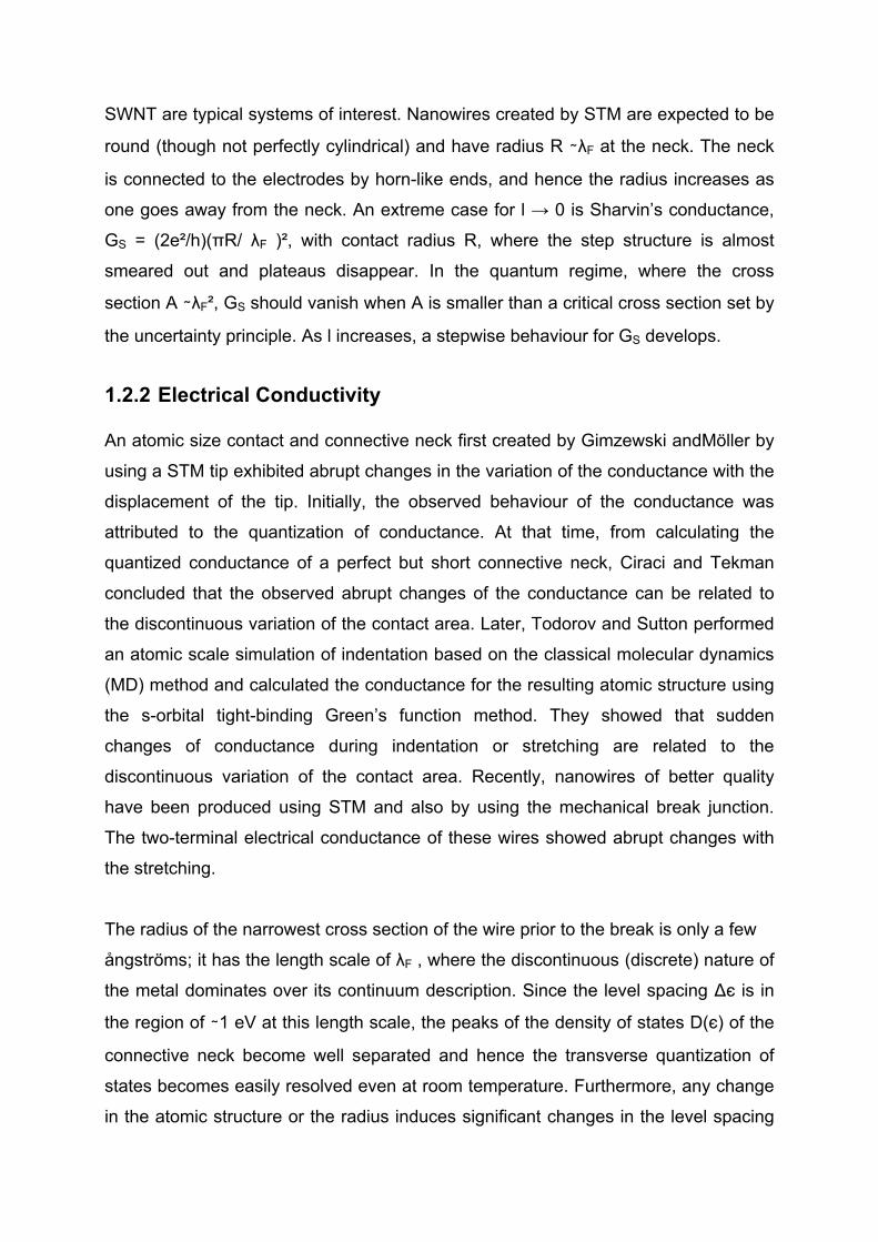
But after further stretching, it recovers with the formation of a new layer. In the
yielding stage, |Fz| decreases abruptly; the cross section of the layer formed at the
end of the yielding stage is abruptly reduced by a few atoms. As a typical example,
the force variation and atomic structure calculated by the MD method are illustrated
in Figure 1-2.
Figure 1-2: The variation of the tensile force Fz (in nanonewtons) with the strain or elongation s along
the z-axis of the nanowire having Cu(001) structure. The stretch s is realized in m discrete steps. The
snapshots show the atomic positions at relevant stretch steps m. The MD simulations are performed
at T = 300K [K. S. Ciraci, A. Buldum, I.P. Batra, Quantum effects in electrical and thermal transport
through nanowires, 2001, Journal of Physics Condensed Matter]
When the neck becomes very narrow (having 3–4 atoms), the yielding is realized,
however, by a single atom jumping from one of the adjacent layers to the interlayer
region.
Under certain circumstances, atoms at the neck form a pentagon that becomes
staggered in different layers. The interlayer atoms make a chain passing through the
centre of the pentagon rings. In this new phase, the elastic and yielding stages are
intermixed and elongation, which is by more than one interlayer distance, can be
accommodated. As the cross section of the wire is further decreased the pentagons
are transformed to a triangle. In the initial stage of pulling off, the single-atom
process, in which individual atoms also migrate from central layers towards the end
layers, can give rise to a small and less discontinuous change in the cross section.
The tendency to minimize the surface area, and hence to reduce the strain energy of
the system, is the main driving force for this type of neck formation. While quasi-
elastic and yielding stages are distinguishable initially, the force variation becomes
more complex and more dependent on the migration of atoms for atomic necks.
Atomic migrations have important implications such as dips in the variation of
conductance with stretch. The simulation studies on metal wires with diameters ∼λF at
the neck, but increasing gradually as one goes away from the neck region, have
shown structural instabilities. Such wires displayed spontaneous thinning of the
necks even in the absence of any tensile strain.
Under prolonged stretching, shortly before the break, the cross section of the neck is
reduced to include only 2–3 atoms. In this case, the hollow-site registry may change
to the top-site registry. This leads to the formation of a bundle of atomic chains (rope)
or of a single atomic chain (see Figure 1-3). We consider this a dramatic change in the
atomic structure of the wire that has important implications. For example, first-
principles calculations indicated that a chain of single Al atoms has an effective
Young modulus stronger than that of the bulk.
Figure 1-3: The top view of three layers at the neck showing atomic positions and their relative
registry at different levels of stretch. m = 15 occurs before the first yielding stage. The atomic positions
in the layers 2, 3 and 4 are indicated by +, • and ◊, respectively. m = 38 and m = 41 occur after the
second yielding stage. m = 46, 47 and m = 49 show the formation of bundle structure (or strands). In
the panels for m = 38–49 the positions of atoms in the third, fourth and fifth (central) layers are
indicated by +, • and ◊, respectively. Atomic chains in a bundle are highlighted by square boxes. [K. S.
Ciraci, A. Buldum, I.P. Batra, Quantum effects in electrical and thermal transport through nanowires,
2001, Journal of Physics Condensed Matter]
1.2.2.2 Electrical conductance of nanowires
The overall features of electrical conductance have been obtained from a statistical
analysis of the results of many consecutive measurements to deduce how frequently
a measured conductance value occurs. Many distribution curves exhibited a peak
near G0 = 2e²/h for metal nanowires, and a relatively broad peak near 3G0, and

almost no significant structure for larger values of conductance. It appears that the
cross section of a connective neck can be reduced down to a single atom just before
the wire breaks. In certain situations, the connective neck can be a monatomic chain
comprising of a few atoms arranged in a row. In this case, a transverse state
quantized in the neck at the Fermi level is coupled to the states of the electrodes and
forms a conducting channel yielding a plateau in the G(s) curve, and hence a peak in
the statistical distribution curve. The step structure for large necks comprising of a
few atoms cannot occur at integer multiples of G0 due to the scattering from
irregularities, and hence due to the channel mixing.
It should be noted that in the course of stretching, elastic and yielding stages repeat;
the surface of the nanowire roughens and deviates strongly from circular symmetry.
The length of the narrowest part of the neck is usually only one or two interlayer
separations, and is connected to the horn-like ends. Under these circumstances, the
quantization is not complete and the contribution of the tunnelling is not negligible.
Results of atomic simulations point to the fact that neither adiabatic evolution of
discrete electronic states, nor perfect circular symmetry can occur in the neck.
Consequently the expected quantized sharp structure shall be smeared out by
channel mixing and tunnelling.
Contradicting these arguments, the changes in the conductance are, however,
abrupt. This controversial situation has been explained by the combined
measurements of the conductance and force variation with the stretch. The abrupt
changes of conductance in the course of stretching coincide with the sudden release
(or relief) of the measured tensile force. The tensile stress is released suddenly
following the yielding stage, whereby the cross section of the wire is reduced
discontinuously, and hence the electronic structure and the electronic level spacing
undergo an abrupt change near the neck. The variation of the conductance, i.e. G(s),
calculated for stretching the nanowire is presented as an example in Figure 1-4.
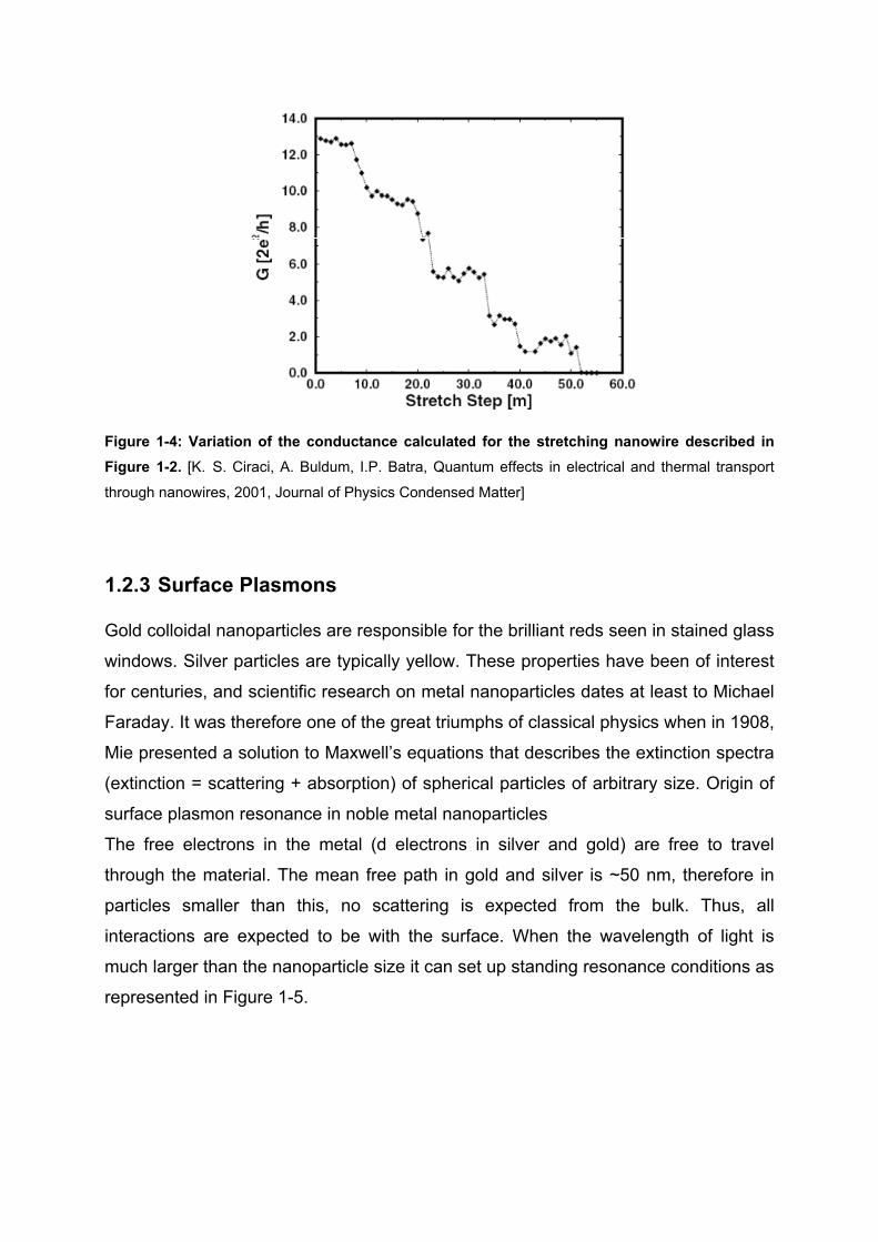
Figure 1-4: Variation of the conductance calculated for the stretching nanowire described in Figure 1-2. [K. S. Ciraci, A. Buldum, I.P. Batra, Quantum effects in electrical and thermal transport
through nanowires, 2001, Journal of Physics Condensed Matter]
1.2.3 Surface Plasmons
Gold colloidal nanoparticles are responsible for the brilliant reds seen in stained glass
windows. Silver particles are typically yellow. These properties have been of interest
for centuries, and scientific research on metal nanoparticles dates at least to Michael
Faraday. It was therefore one of the great triumphs of classical physics when in 1908,
Mie presented a solution to Maxwell’s equations that describes the extinction spectra
(extinction = scattering + absorption) of spherical particles of arbitrary size. Origin of
surface plasmon resonance in noble metal nanoparticles
The free electrons in the metal (d electrons in silver and gold) are free to travel
through the material. The mean free path in gold and silver is ~50 nm, therefore in
particles smaller than this, no scattering is expected from the bulk. Thus, all
interactions are expected to be with the surface. When the wavelength of light is
much larger than the nanoparticle size it can set up standing resonance conditions as
represented in Figure 1-5.

Figure 1-5: Schematic of plasmon oscillation for a sphere, showing the displacement of the
conduction electron charge cloud relative to the nuclei. [K. Lance Kelly, E. Coronado, L.L. Zhao, G.C.
Schatz, The Optical Properties of Metal Nanoparticles: The Influence of Size, Shape, and Dielectric
Environment, 2003, Journal of Physical Chemistry]
Light in resonance with the surface plasmon oscillation causes the free-electrons in
the metal to oscillate. As the wave front of the light passes, the electron density in the
particle is polarized to one surface and oscillates in resonance with the light’s
frequency causing a standing oscillation. The resonance condition is determined from
absorption and scattering spectroscopy and is found to depend on the shape, size,
and dielectric constants of both the metal and the surrounding material. This is
referred to as the surface plasmon resonance, since it is located at the surface. As
the shape or size of the nanoparticle changes, the surface geometry changes
causing a shift in the electric field density on the surface. This causes a change in the
oscillation frequency of the electrons, generating different cross-sections for the
optical properties including absorption and scattering.
Changing the dielectric constant of the surrounding material will have an effect on the
oscillation frequency due to the varying ability of the surface to accommodate
electron charge density from the nanoparticles. Changing the solvent will change the
dielectric constant, but the capping material is most important in determining the shift
of the plasmon resonance due to the local nature of its effect on the surface of the
nanoparticle. Chemically bonded molecules can be detected by the observed change
they induce in the electron density on the surface, which results in a shift in the
surface plasmon absorption maximum. This is the basis for the use of noble metal
nanoparticles as sensitive sensors. Mie originally calculated the surface plasmon
resonance by solving Maxwell’s equations for small spheres interacting with an
electromagnetic field. Gan was able to extend this theory to apply to ellipsoidal
geometries. Modern methods using the discrete dipole approximation (DDA) allow
one to calculate the surface plasmon resonance absorption for arbitrary geometries.
Calculation of the longitudinal plasmon resonance for gold nanorods generates an

increase in the intensity and wavelength maximum as the aspect ratio (length divided
by width) increases. Thus, the plasmon resonance can be tuned across the visible
region by changing the aspect ratio. The increase in the intensity of the surface
plasmon resonance absorption leads to an enhancement of the electric field, as
exploited in many applications.
1.2.3.1 Dipole plasmon resonances
When a small spherical metallic nanoparticle is irradiated by light, the oscillating
electric field causes the conduction electrons to oscillate coherently (Figure 1-5).
When the electron cloud is displaced relative to the nuclei, a restoring force arises
from Coulomb attraction between electrons and nuclei that results in oscillation of the
electron cloud relative to the nuclear framework. The oscillation frequency is
determined by four factors: the density of electrons, the effective electron mass, and
the shape and size of the charge distribution. The collective oscillation of the
electrons is called the dipole plasmon resonance of the particle (sometimes denoted
“dipole particle plasmon resonance” to distinguish from plasmon excitation that can
occur in bulk metal or metal surfaces). Higher modes of plasmon excitation can
occur, such as the quadrupole mode where half of the electron cloud moves parallel
to the applied field and half moves antiparallel. For a metal like silver, the plasmon
frequency is also influenced by other electrons such as those in d-orbitals, and this
prevents the plasmon frequency from being easily calculated using electronic
structure calculations. However, it is not hard to relate the plasmon frequency to the
metal dielectric constant, which is a property that can be measured as a function of
wavelength for bulk metal.
To relate the dipole plasmon frequency of a metal nanoparticle to the dielectric
constant, we consider the interaction of light with a spherical particle that is much
smaller than the wavelength of light. Under these circumstances, the electric field of
the light can be taken to be constant, and the interaction is governed by electrostatics
rather than electrodynamics. This is often called the quasistatic approximation, as we
use the wavelength-dependent dielectric constant of the metal particle, єi, and of the
surrounding medium, є0, in what is otherwise an electrostatic theory.
Let’s denote the electric field of the incident electromagnetic wave by the vector Eo.
We take this constant vector to be in the x direction so that Eo = Eo x , where x is a
unit vector. To determine the electromagnetic field surrounding the particle, we solve
LaPlace’s equation (the fundamental equation of electrostatics), ϕ2∇ = 0, where φ is
the electric potential and the field E is related to φ by E = -∇φ. In developing this
solution, we apply two boundary conditions: (i) that φ is continuous at the sphere
surface and (ii) that the normal component of the electric displacement D is also
continuous, where D = є E.
It is not difficult to show that the general solution to the LaPlace equation has angular
solutions which are just the spherical harmonics. In addition, the radial solutions are
of the form rl and r-(l +1), where l is the familiar angular momentum label (l = 0, 1, 2,...)
of atomic orbitals. If we restrict our considerations for now to just the l = 1 solution
and if Eo is in the x direction, the potential is simply φ = A r sinθ cosΦ inside the
sphere (r < a) and φ = (-Eor + B/r²) sinθ cosΦ outside the sphere (r > a), where A and
B are constants to be determined. If these solutions are inserted into the boundary
conditions and the resulting φ is used to determine the field outside the sphere, Eout,
we get
⎥⎦⎤
⎢⎣⎡ ++−−= )(3
53 zzyyxxrx
rxExEE ooout α (1. 12)
Where α is the sphere polarizability and x , y , and z are the usual unit vectors. We
note that the first term in eq ⎥⎦⎤
⎢⎣⎡ ++−−= )(3
53 zzyyxxrx
rxExEE ooout α (1. 12) is
the applied field and the second is the induced dipole field (induced dipole moment =
αEo) that results from polarization of the conduction electron density.
For a sphere with the dielectric constants indicated above, the LaPlace equation
solution shows that the polarizability is
3agd=α (1. 13)
with
0
0
2∈+∈∈−∈
=i
idg (1. 14)
Although the dipole field in eq ⎥⎦⎤
⎢⎣⎡ ++−−= )(3
53 zzyyxxrx
rxExEE ooout α (1. 12) is
that for a static dipole, the more complete Maxwell equation solution shows that this

is actually a radiating dipole, and thus, it contributes to extinction and Rayleigh
scattering by the sphere. This leads to extinction and scattering efficiencies given by
)Im(4 dext gxQ = (1. 15)
24
38
dsca gxQ = (1. 16)
where x = 2πa(є0)1/2/λ. The efficiency is the ratio of the cross-section to the
geometrical cross-section πa². Note that the factor gd from eq 0
0
2∈+∈∈−∈
=i
idg
(1.
14) plays the key role in determining the wavelength dependence of these cross-
sections, as the metal dielectric constant єi is strongly dependent on wavelength.
1.2.3.2 Quadrupole plasmon Resonances
For larger particles, higher multipoles, especially the quadrupole term (l=2) become
important to the extinction and scattering spectra. Using the same notation as above
and including the l=2 term in the LaPlace equation solution, the resulting field outside
the sphere, Eout, now can be expressed as
( ) ( ) ( ) ⎥⎦
⎤⎢⎣
⎡⎥⎦⎤
⎢⎣⎡ ++−
+−++−−++= zxzyyxx
rz
rzzxxEzzyyxx
rx
rxEzzxxikExEE ooooout ²²53
7553 βα
(1. 17)
and the quadrupole polarizability is
5agd=α (1. 18)
0
03 / 2i
di
g ε εε ε
−=
+ (1. 19)
Note that the denominator of eq 0
03 / 2i
di
g ε εε ε
−=
+ (1. 19) contains the factor 3/2
while in eq 0
0
2∈+∈∈−∈
=i
idg
(1. 14) the corresponding number is 2. These factors arise
from the exponents in the radial solutions to LaPlace’s equation, e.g., the factors rl
and r -(l +1) that were discussed above. For dipole excitation, we have l=1, and the
magnitude of the ratio of the exponents is (l + 1)/l = 2, while for quadrupole excitation
(l + 1)/l = 3/2. Higher partial waves work analogously.

Following the same derivation, we get the following quasistatic (dipole + quadrupole)
expressions for the extinction and Rayleigh scattering efficiencies:
( )² ²4 Im 112 30ext d q ix xQ x g g ε⎡ ⎤= + + −⎢ ⎥⎣ ⎦
(1. 20)
4 422 248 13 240 900ext d q i
x xQ x g g ε⎧ ⎫
= + + −⎨ ⎬⎩ ⎭
(1. 21)
1.2.3.3 Extinction for silver spheres
We now evaluate the extinction cross-section using the quasistatic expressions, eqs
(1.24), (1.25) and (1.29), (1.30) as well as the exact (Mie) theory. We take dielectric
constants for silver that are plotted in Figure 1-6 a) and the external dielectric
constant is assumed to be 1 (i.e., a particle in a vacuum). The resulting efficiencies
for 30 and 60 nm spheres are plotted in Figure 1-6 b),c), respectively.
Figure 1-6: (a) Real and imaginary part of silver dielectric constants as function of wavelength. (b)
Extinction efficiency, i.e., the ratio of the extinction cross-section to the area of the sphere, as obtained

from quasistatic theory for a silver sphere whose radius is 30 nm. (c) The corresponding efficiency for
a 60 nm particle, including for quadrupole effects, and correcting for finite wavelength effects. In b and
c, the exact Mie theory result is also plotted. [K. Lance Kelly, E. Coronado, L.L. Zhao, G.C. Schatz,
The Optical Properties of Metal Nanoparticles: The Influence of Size, Shape, and Dielectric
Environment, 2003, Journal of Physical Chemistry]
The cross-section in Figure 1-6 b) shows a sharp peak at 367nm, with a good match
between quasistatic and Mie theory. This peak is the dipole surface plasmon
resonance, and it occurs when the real part of the denominator in eq 0
0
2∈+∈∈−∈
=i
idg
(1. 14) vanishes, corresponding to a metal dielectric constant whose real part
is -2. For particles that are not in a vacuum, the plasmon resonance condition
becomes
Re єi/є0= -2, and because the real part of the silver dielectric constant decreases with
increasing wavelength (Figure 1-6 a), the plasmon resonance wavelength for є0 > 1 is
longer than in a vacuum. The plasmon resonance wavelength also gets longer if the
particle size is increased above 30 nm. This is due to additional electromagnetic
effects that will be discussed later.
Figure 1-6 c) presents the l = 2 quasistatic (dipole + quadrupole) cross-section as
well as the full Mie theory result for a radius 60 nm sphere. The quasistatic result also
includes a finite wavelength correction. We see that the dipole plasmon wavelength
has shifted to the red, and there is now a distinct quadrupole resonance peak at 357
nm. This quadrupole peak occurs when the real part of the denominator in eq (1.28)
vanishes, corresponding to a metal dielectric constant whose real part is -3/2. For a
sphere of this size, there are clear differences between the quasistatic and the Mie
theory results; however, the important features are retained. Although Mie theory is
not a very expensive calculation, the quasistatic expressions are convenient to use
when only qualitative information is needed.
1.2.3.4 Electromagnetic fields for spherical particles
So far, we have emphasized the calculation of extinction and Rayleigh scattering
cross-section; however, for certain properties, such as surface enhanced Raman
spectroscopy,SERS, and hyper-Raman scattering (HRS) intensities, it is the
electromagnetic field at or near the particle surfaces that determines the measured
intensity. Thus, if E(ω) is the local field for frequency ω, then the SERS intensity is

determined by 22 )'()( ωω EE where ω’ is the Stokes-shifted frequency and the
brackets are used to denote an average over the particle surface. The HRS intensity
is similarly (but approximately) determined by 24 )2()( ωω EE . Also, when one
makes an aggregate or array of metal nanoparticles, the interaction between the
particles is determined by the polarization induced in each particle due to the fields E arising from all of the other particles.
At the dipole (dipole + quadrupole) level, the field outside a particle is given by eq
⎥⎦⎤
⎢⎣⎡ ++−−= )(3
53 zzyyxxrx
rxExEE ooout α (1. 12) et
( ) ( ) ( ) ⎥⎦
⎤⎢⎣
⎡⎥⎦⎤
⎢⎣⎡ ++−
+−++−−++= zxzyyxx
rz
rzzxxEzzyyxx
rx
rxEzzxxikExEE ooooout ²²53
7553 βα
(1. 17). These expressions determine the near-fields at the particle surfaces quite
accurately for small enough particles; however, the field beyond 100 nm from the
center of the particle exhibits radiative contributions that are not contained in these
equations. To describe these, we need to replace the dipole or quadrupole field by its
radiative counterpart. In the case of the dipole field, this is given by
( )53
)(3²)1(²r
PrrPrikrer
prrekE ikrikrdipole
•−−+
××= (1. 22)
where P is the dipole moment. Note that this reduces to the static field in eq
⎥⎦⎤
⎢⎣⎡ ++−−= )(3
53 zzyyxxrx
rxExEE ooout α
(1. 12) in the limit k→0 where only the term
in square brackets remains. However, at long range, the first term becomes dominant
as it falls off more slowly with r than the second.
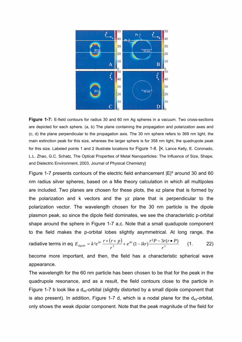
Figure 1-7: E-field contours for radius 30 and 60 nm Ag spheres in a vacuum. Two cross-sections
are depicted for each sphere. (a, b) The plane containing the propagation and polarization axes and
(c, d) the plane perpendicular to the propagation axis. The 30 nm sphere refers to 369 nm light, the
main extinction peak for this size, whereas the larger sphere is for 358 nm light, the quadrupole peak
for this size. Labeled points 1 and 2 illustrate locations for Figure 1-8. [K. Lance Kelly, E. Coronado,
L.L. Zhao, G.C. Schatz, The Optical Properties of Metal Nanoparticles: The Influence of Size, Shape,
and Dielectric Environment, 2003, Journal of Physical Chemistry]
Figure 1-7 presents contours of the electric field enhancement |E|² around 30 and 60
nm radius silver spheres, based on a Mie theory calculation in which all multipoles
are included. Two planes are chosen for these plots, the xz plane that is formed by
the polarization and k vectors and the yz plane that is perpendicular to the
polarization vector. The wavelength chosen for the 30 nm particle is the dipole
plasmon peak, so since the dipole field dominates, we see the characteristic p-orbital
shape around the sphere in Figure 1-7 a,c. Note that a small quadupole component
to the field makes the p-orbital lobes slightly asymmetrical. At long range, the
radiative terms in eq ( )53
)(3²)1(²r
PrrPrikrer
prrekE ikrikrdipole
•−−+
××= (1. 22)
become more important, and then, the field has a characteristic spherical wave
appearance.
The wavelength for the 60 nm particle has been chosen to be that for the peak in the
quadrupole resonance, and as a result, the field contours close to the particle in
Figure 1-7 b look like a dxz-orbital (slightly distorted by a small dipole component that
is also present). In addition, Figure 1-7 d, which is a nodal plane for the dxz-orbital,
only shows the weak dipolar component. Note that the peak magnitude of the field for
the 30 nm particle occurs at the particle surface, along the polarization direction. This
peak is over 50 times the size of the applied field, while that for the 60 nm particle is
over 25 times larger. This is responsible for the electromagnetic enhancements that
are seen in SERS, and they also lead to greatly enhanced HRS.
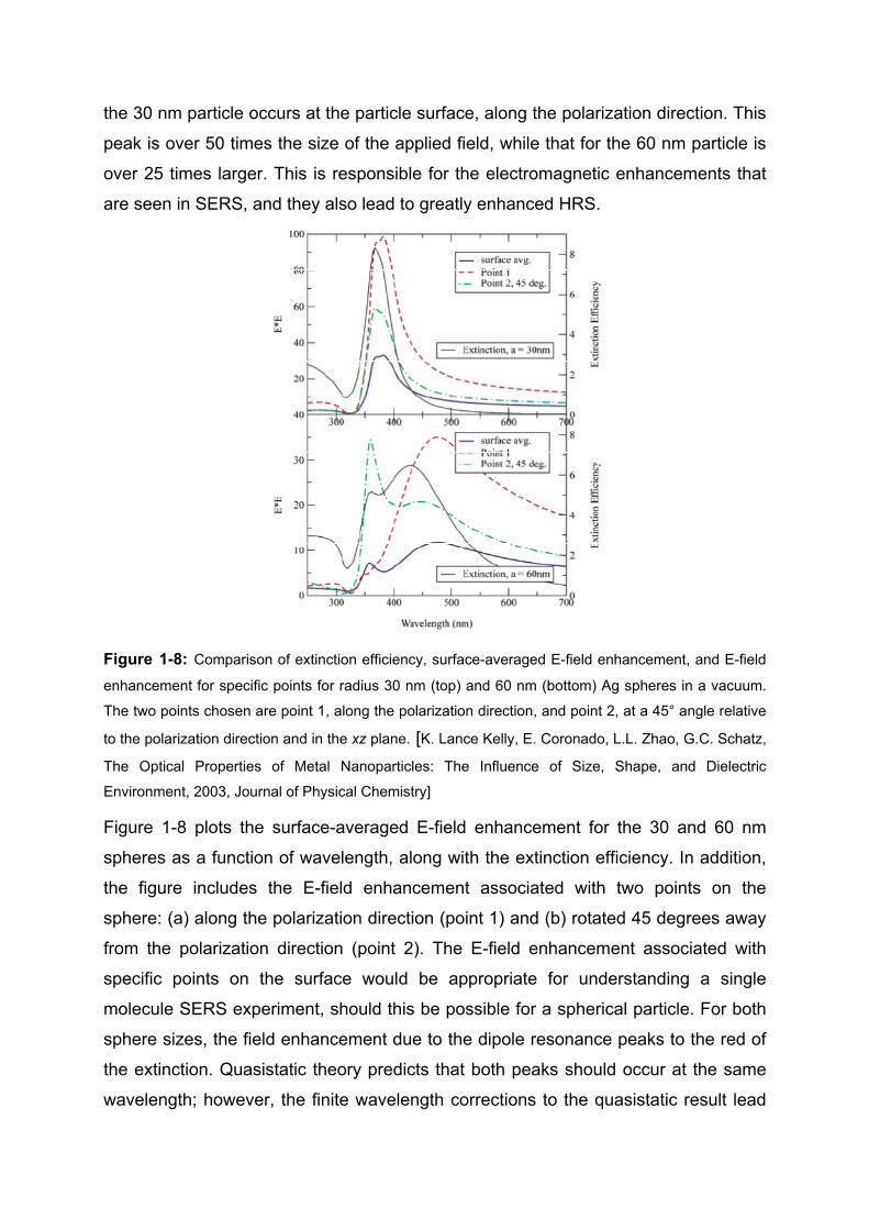
Figure 1-8: Comparison of extinction efficiency, surface-averaged E-field enhancement, and E-field
enhancement for specific points for radius 30 nm (top) and 60 nm (bottom) Ag spheres in a vacuum.
The two points chosen are point 1, along the polarization direction, and point 2, at a 45° angle relative
to the polarization direction and in the xz plane. [K. Lance Kelly, E. Coronado, L.L. Zhao, G.C. Schatz,
The Optical Properties of Metal Nanoparticles: The Influence of Size, Shape, and Dielectric
Environment, 2003, Journal of Physical Chemistry]
Figure 1-8 plots the surface-averaged E-field enhancement for the 30 and 60 nm
spheres as a function of wavelength, along with the extinction efficiency. In addition,
the figure includes the E-field enhancement associated with two points on the
sphere: (a) along the polarization direction (point 1) and (b) rotated 45 degrees away
from the polarization direction (point 2). The E-field enhancement associated with
specific points on the surface would be appropriate for understanding a single
molecule SERS experiment, should this be possible for a spherical particle. For both
sphere sizes, the field enhancement due to the dipole resonance peaks to the red of
the extinction. Quasistatic theory predicts that both peaks should occur at the same
wavelength; however, the finite wavelength corrections to the quasistatic result lead
to depolarization of the plasmon excitation on the blue side of the extinction peak,
resulting in a smaller average field and a red-shifted peak.
For the smaller sphere (top panel of Figure 1-8), the E-field enhancement associated
with point 1 is about three times larger than the surface-averaged value, and the
lineshapes are the same. Point 2 shows a smaller enhancement, and it peaks toward
the blue, indicating the influence of a weak quadrupole resonance. For the larger
sphere (bottom), the maximum for point 1 is about 3.5 times greater than the surface
average for the dipole peak. For point 2, we see a maximum at the quadrupole
resonance wavelength, and the enhancement is about three times greater than for
the quadrupole peak in the surface-averaged result. Thus, for the larger sphere, it is
possible for the largest SERS enhancement to be at a location on the surface that is
not along the polarization direction.
1.3 Carbon Nanotubes
Nanotubes were discovered by Iijima in the form of multiple coaxial carbon fullerene
shells (multi-wall nanotubes, MWNTs). Later, in 1993 single fullerene shells (single-
wall nanotubes, SWNTs) were synthesized using transition metal catalysts. A
nanotube can be simply described as a sheet of graphite (or graphene) coaxially
rolled to create a cylindrical surface (as shown in Figure 1-9(a)).
Figure 1-9: (a) A single-wall nanotube is graphene wrapped on a cylinder surface. (b) Nanotubes are
described by a set of two integers (n, m) which indicate the graphite lattice vector components. A
chiral vector can be defined as C = na1 + ma2. Tubes are called ‘zigzag’ if either one of the integers is
zero (n, 0) or called ‘armchair’ if both integers are equal (n, n). [K. S. Ciraci, A. Buldum, I.P. Batra,
Quantum effects in electrical and thermal transport through nanowires, 2001, Journal of Physics
Condensed Matter]
In this way the 2D hexagonal lattice of grapheme is mapped onto a cylinder of radius
R. The mapping can be realized with different helicities resulting in different
nanotubes. Each nanotube is characterized by a set of two integers (n, m) indicating
the components of the chiral vector C = na1 + ma2 in terms of the 2D hexagonal
Bravais lattice vectors of graphene, a1 and a2, as illustrated in Figure 1-9(b). The chiral
vector is a circumferential vector and the tube is obtained by folding the graphene
such that the two ends of C are coincident. The radius of the tube is given in terms of
(n, m) through the relation π2/nm m² n²a R 0 ++= , where |a1| = |a2| = a0. When C
involves only a1 (corresponding to (n, 0)) the tube is called ‘zigzag’, and if C involves
both a1 and a2 with n = m (corresponding to (n, n)) the tube is called ‘armchair’. The
chiral (n, n) vector is rotated by 30 relative to that of the zigzag (n, 0) tube. SWNTs
are found in the form of nanoropes, each rope consisting of up to a few hundred
nanotubes arranged in a hexagonal lattice structure.
1.3.1 Electronic structure
As a nanotube is in the form of a wrapped sheet of graphite, its electronic structure is
analogous to the electronic structure of a graphene. Graphene has the lowest π∗-
conduction band and the highest π-valence band, which are separated by a gap in
the entire hexagonal Brillouin zone (BZ) except at its K corners where they cross. In
this respect, graphene lies between a semiconductor and a metal with Fermi points at
the corners of the BZ. You can imagine an unrolled, open form of nanotube, which is
graphene subject to periodic boundary conditions on the chiral vector. This in turn
imposes quantization on the wave vector. This is known as zone folding, whereby the
BZ is sliced with parallel lines of wave vectors, leading to subband structure. A
nanotube’s electronic structure can thus be viewed as a zone-folded version of the
electronic band structure of the graphene. When these parallel lines of nanotube
wave vectors pass through the corners, the nanotube is metallic. Otherwise, the
nanotube is a semiconductor with a gap of about 1 eV, which is reduced as the
diameter of the tube increases. Within this simple approach, (n, m) nanotubes are
metallic if n − m = 3× integer. Consequently, all armchair tubes are metallic. The
conclusion that you draw from the above paragraph is that the electronic structures of
nanotubes are determined by their chirality and diameter, i.e. simply by their chiral
vectors C.
The first theoretical calculations were performed and the above simple understanding
was provided much earlier than the first conclusive experiments were carried out . In

these early calculations, a simple one-band π-orbital tight-binding model was used.
However, different calculations have been at variance on the values of the band gap.
For example, while the σ∗–π∗ hybridization due to the curvature can be treated well
by calculations, simple tight-binding methods may have limitations for small-radius
nanotubes.
Figure 1-10: (a) The band structure, (b) density of states and (c) conductance of a (10, 10) nanotube.
The tight-binding model is used to derive the electronic structure. The conductance is calculated using
the Green’s function approach with the Landauer formalism. [K. S. Ciraci, A. Buldum, I.P. Batra,
Quantum effects in electrical and thermal transport through nanowires, 2001, Journal of Physics
Condensed Matter]
In Figure 1-10(a) and (b) the band structure and density of states (DOS) of a (10, 10)
tube are given, based on a tight-binding calculation. Samples prepared by laser
vaporization consist predominantly of (10, 10) metallic armchair SWNTs. As can be
seen in Figure 1-10 (a), band crossing is allowed, and the bonding π- and antibonding
π∗-states cross the Fermi level at kz = 2π/3.
In Figure 1-10 (b) the density of states is plotted for the (10, 10) tube. The E−1/2-
singularities which are typical for 1D energy bands appear at the band edges. The
curvature of nanotubes introduces hybridization also between sp2 and sp3 orbitals,
but these effects are small when the radius of a SWNT is large. However, the π∗-
and σ∗-state mixing was enhanced for small-radius zigzag SWNTs. Recently, it has
been shown that the electronic properties of a SWNT can undergo dramatic changes
owing to the elastic deformations. For example, the band gap of a semiconducting
SWNT can be reduced or even closed by the elastic radial deformation. The gap
modification and the eventual strain-induced metallization seem to offer new
alternatives for reversible and tunable quantum structures and nanodevices.
1.3.2 Quantum transport properties
A nanotube can be an ideal quantum wire for electronic transport; two subbands
crossing at the Fermi level should nominally give rise to two conducting channels.
Under ideal conditions each channel can carry current with unit quantum
conductance 2e2/h; the total resistance of an individual SWNT would be h/4e2 or ∼6
kΩ. The contribution of each subband to the total conductance is clearly seen in
Figure 1-10 (c) illustrating the calculated conductance of the (10, 10) nanotube.
The first electronic transport measurements of nanotubes were carried out using
MWNTs. These measurements found MWNTs to be highly resistive due to defect
scattering and weak localization. The first electronic transport measurements of
individual SWNTs and nanoropes were performed by Tans et al [] and Bockrath et al
[]. In these measurements nanotubes or nanoropes were placed on an insulating
(oxidized silicon) substrate containing metallic electrodes.
(a) An AFM image of a carbon nanotube on top
of a Si/SiO2 substrate with Pt electrodes. A gate
voltage Vg is applied to the third electrode in the
upper left corner to vary the electrostatic potential
of the nanotube.
(b) Current–voltage curves of nanotubes for
different Vg values (A: 88.2 mV, B: 104.1 mV and
C: 120.0 mV).
Figure 1-11: a) and b) [K. S. Ciraci, A. Buldum, I.P. Batra, Quantum effects in electrical and thermal
transport through nanowires, 2001, Journal of Physics Condensed Matter]
In Figure 1-11 (a) an AFM image of an individual SWNT on a silicon dioxide substrate
is shown with two Pt electrodes. A gate voltage Vg is applied to the third electrode in
the upper left corner to shift the electrostatic potential of the nanotube. The
measurements were performed at 5 mK and step-like features are observed in
current–voltage curves shown in Figure 1-11 (b). Note that the voltage scale is mV
and these steps are not due to the quantized increase of conductance with subbands
shown in Figure 1-10 (c). These steps are due to resonant tunnelling of electrons to the
states of a finite nanotube. The presence of metallic electrodes introduces significant
contact resistances and changes the bent part of the nanotube into a quantum-dot-
like structure. The same phenomena were seen in individual ropes of nanotubes with
oscillations in the conductance at low temperatures.
An interesting transport experiment was performed by Frank et al []. MWNTs were
dipped into liquid metal with the help of a scanning probe microscope tip and the
conductance was measured simultaneously. Figure 1-12 (a) and Figure 1-12 (b)
show the nanotube contact used in the measurements.
Figure 1-12: (A) A transmission electron micrograph (TEM) image of the end of a nanotube fibre
which consists of carbon nanotubes and small graphitic particles. (B) A schematic diagram of the
experimental set-up. Nanotubes are lowered under SPM control to a liquid metal surface. (C) Variation
of conductance with nanotube fibre position. Plateaus are observed corresponding to additional
nanotubes coming into contact with the liquid metal. [K. S. Ciraci, A. Buldum, I.P. Batra, Quantum
effects in electrical and thermal transport through nanowires, 2001, Journal of Physics Condensed
Matter]
The nanotubes were straight with lengths of 1 to 10 μm. As the nanotubes were
dipped into the liquid metal one by one, the conductance increased in steps of 2e2/h as shown in Figure 1-12(c). Each step corresponds to an additional nanotube coming
into contact with liquid metal. The electronic transport is found to be ballistic, since
the step heights do not depend on the different lengths of nanotubes coming into
contact with the metal.
1.3.3 Nanotube junctions and devices
Current trends in microelectronics are to produce smaller and faster devices. Owing
to the novel and unusual mechanical and electronic properties, carbon nanotubes
appear to be potential candidates for meeting the demands of nanotechnologies.
There are already nanodevices which use nanotubes. Single-electron transistors
were produced by using metallic tubes; the devices formed therefrom have operated
at low temperatures. For example, a field-effect transistor that consists of a
semiconductor nanotube and operates at room temperature. The nanotube placed on
two metal electrodes and a Si substrate which is covered with SiO2 is used as a
back-gate. The nanotube is switched from a conducting to an insulating state by
applying a gate voltage.
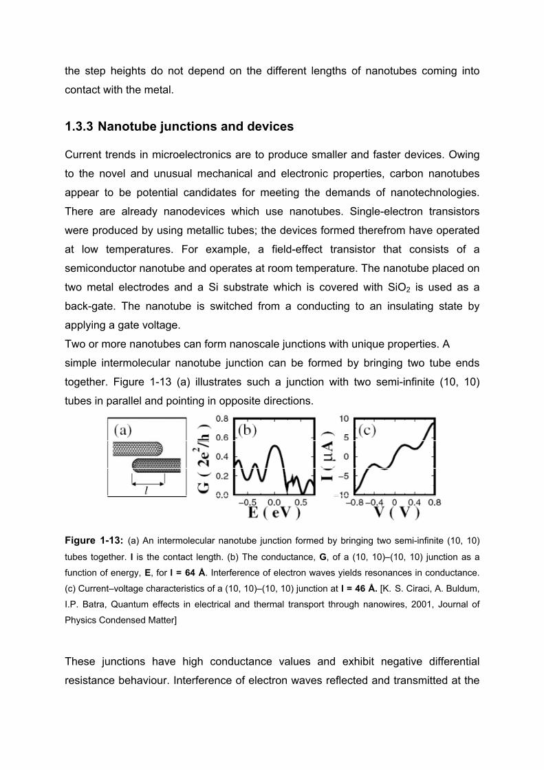
Two or more nanotubes can form nanoscale junctions with unique properties. A
simple intermolecular nanotube junction can be formed by bringing two tube ends
together. Figure 1-13 (a) illustrates such a junction with two semi-infinite (10, 10)
tubes in parallel and pointing in opposite directions.
Figure 1-13: (a) An intermolecular nanotube junction formed by bringing two semi-infinite (10, 10)
tubes together. l is the contact length. (b) The conductance, G, of a (10, 10)–(10, 10) junction as a
function of energy, E, for l = 64 Å. Interference of electron waves yields resonances in conductance.
(c) Current–voltage characteristics of a (10, 10)–(10, 10) junction at l = 46 Å. [K. S. Ciraci, A. Buldum,
I.P. Batra, Quantum effects in electrical and thermal transport through nanowires, 2001, Journal of
Physics Condensed Matter]
These junctions have high conductance values and exhibit negative differential
resistance behaviour. Interference of electron waves reflected and transmitted at the
tube ends gives rise to the resonances in conductance shown in Figure 1-13 (b). The
current–voltage characteristics of this junction presented in Figure 1-13 (c) show a
negative differential resistance effect, which may have applications in high-speed
switching, memory and amplification devices.
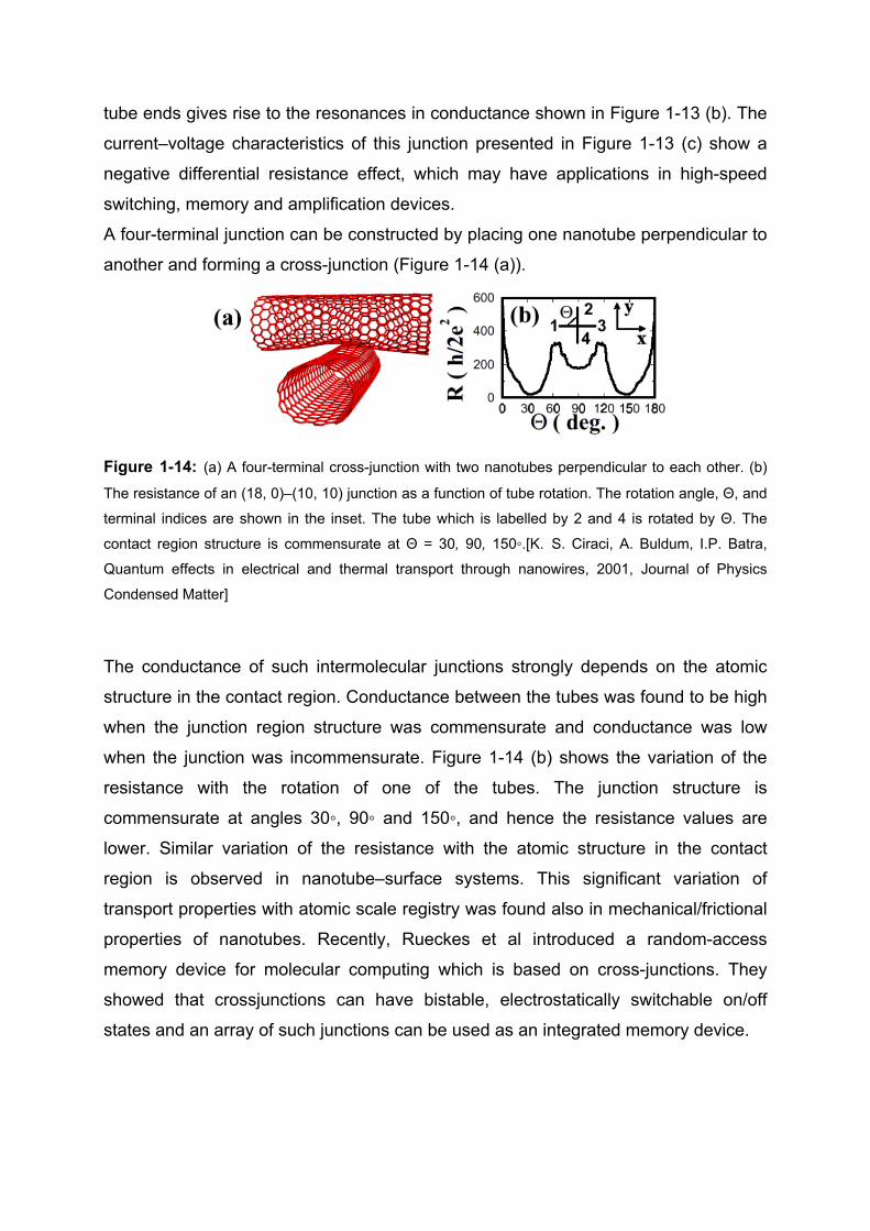
A four-terminal junction can be constructed by placing one nanotube perpendicular to
another and forming a cross-junction (Figure 1-14 (a)).
Figure 1-14: (a) A four-terminal cross-junction with two nanotubes perpendicular to each other. (b)
The resistance of an (18, 0)–(10, 10) junction as a function of tube rotation. The rotation angle, Θ, and
terminal indices are shown in the inset. The tube which is labelled by 2 and 4 is rotated by Θ. The
contact region structure is commensurate at Θ = 30, 90, 150.[K. S. Ciraci, A. Buldum, I.P. Batra,
Quantum effects in electrical and thermal transport through nanowires, 2001, Journal of Physics
Condensed Matter]
The conductance of such intermolecular junctions strongly depends on the atomic
structure in the contact region. Conductance between the tubes was found to be high
when the junction region structure was commensurate and conductance was low
when the junction was incommensurate. Figure 1-14 (b) shows the variation of the
resistance with the rotation of one of the tubes. The junction structure is
commensurate at angles 30, 90 and 150, and hence the resistance values are
lower. Similar variation of the resistance with the atomic structure in the contact
region is observed in nanotube–surface systems. This significant variation of
transport properties with atomic scale registry was found also in mechanical/frictional
properties of nanotubes. Recently, Rueckes et al introduced a random-access
memory device for molecular computing which is based on cross-junctions. They
showed that crossjunctions can have bistable, electrostatically switchable on/off
states and an array of such junctions can be used as an integrated memory device.
1.4 Semiconductor
1.4.1 Introduction
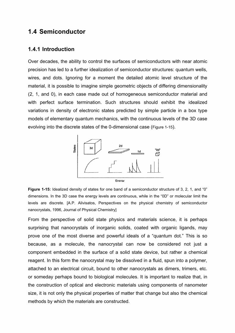
Over decades, the ability to control the surfaces of semiconductors with near atomic
precision has led to a further idealization of semiconductor structures: quantum wells,
wires, and dots. Ignoring for a moment the detailed atomic level structure of the
material, it is possible to imagine simple geometric objects of differing dimensionality
(2, 1, and 0), in each case made out of homogeneous semiconductor material and
with perfect surface termination. Such structures should exhibit the idealized
variations in density of electronic states predicted by simple particle in a box type
models of elementary quantum mechanics, with the continuous levels of the 3D case
evolving into the discrete states of the 0-dimensional case (Figure 1-15).
Figure 1-15: Idealized density of states for one band of a semiconductor structure of 3, 2, 1, and “0”
dimensions. In the 3D case the energy levels are continuous, while in the “0D” or molecular limit the
levels are discrete. [A.P. Alivisatos, Perspectives on the physical chemistry of semiconductor
nanocrystals, 1996, Journal of Physical Chemistry]
From the perspective of solid state physics and materials science, it is perhaps
surprising that nanocrystals of inorganic solids, coated with organic ligands, may
prove one of the most diverse and powerful ideals of a “quantum dot.” This is so
because, as a molecule, the nanocrystal can now be considered not just a
component embedded in the surface of a solid state device, but rather a chemical
reagent. In this form the nanocrystal may be dissolved in a fluid, spun into a polymer,
attached to an electrical circuit, bound to other nanocrystals as dimers, trimers, etc.
or someday perhaps bound to biological molecules. It is important to realize that, in
the construction of optical and electronic materials using components of nanometer
size, it is not only the physical properties of matter that change but also the chemical
methods by which the materials are constructed.
1.4.2 Band Gap modification
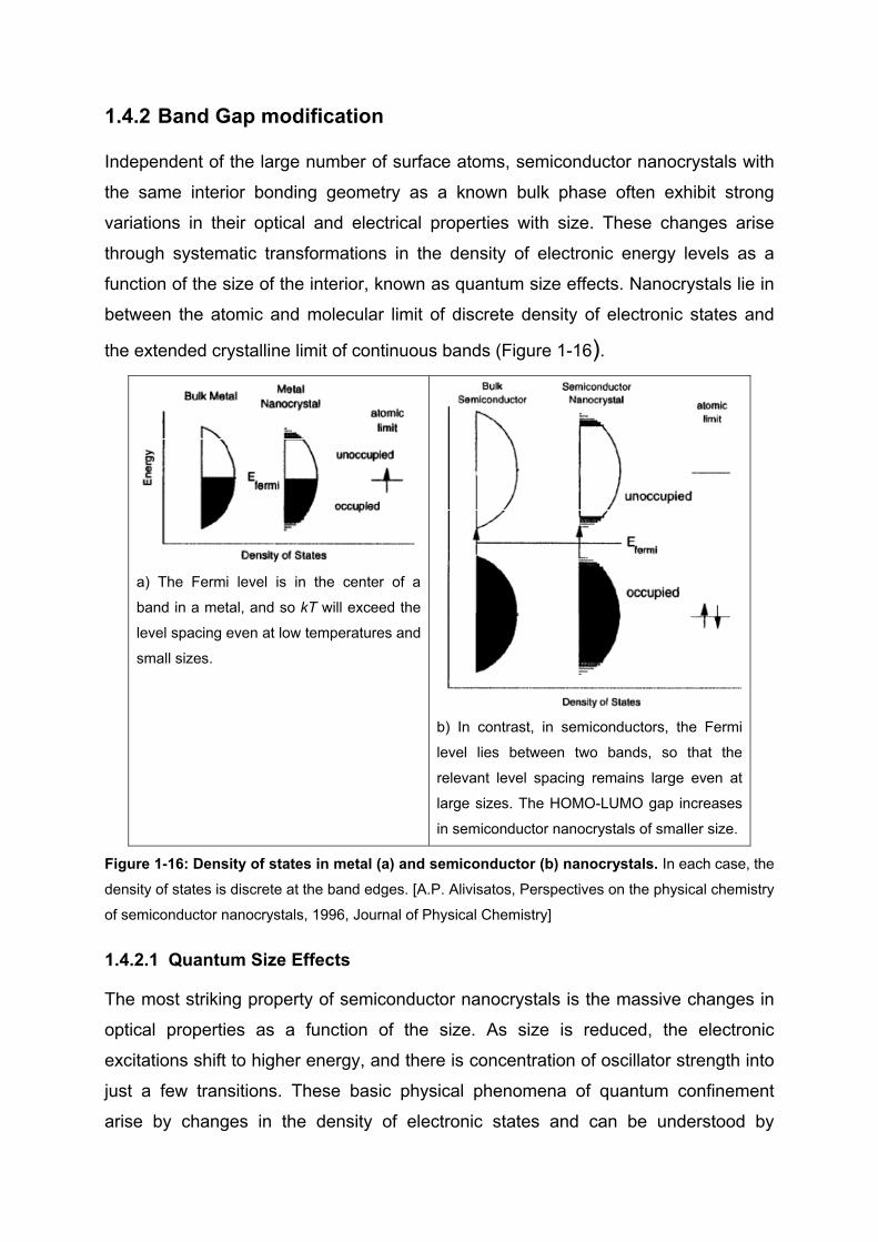
Independent of the large number of surface atoms, semiconductor nanocrystals with
the same interior bonding geometry as a known bulk phase often exhibit strong
variations in their optical and electrical properties with size. These changes arise
through systematic transformations in the density of electronic energy levels as a
function of the size of the interior, known as quantum size effects. Nanocrystals lie in
between the atomic and molecular limit of discrete density of electronic states and
the extended crystalline limit of continuous bands (Figure 1-16).
a) The Fermi level is in the center of a
band in a metal, and so kT will exceed the
level spacing even at low temperatures and
small sizes.
b) In contrast, in semiconductors, the Fermi
level lies between two bands, so that the
relevant level spacing remains large even at
large sizes. The HOMO-LUMO gap increases
in semiconductor nanocrystals of smaller size.
Figure 1-16: Density of states in metal (a) and semiconductor (b) nanocrystals. In each case, the
density of states is discrete at the band edges. [A.P. Alivisatos, Perspectives on the physical chemistry
of semiconductor nanocrystals, 1996, Journal of Physical Chemistry]
1.4.2.1 Quantum Size Effects
The most striking property of semiconductor nanocrystals is the massive changes in
optical properties as a function of the size. As size is reduced, the electronic
excitations shift to higher energy, and there is concentration of oscillator strength into
just a few transitions. These basic physical phenomena of quantum confinement
arise by changes in the density of electronic states and can be understood by
considering the relationship between position and momentum in free and confined
particles:
2/≥ΔΔ xp (1. 23)
For a free particle or a particle in a periodic potential, the energy and the crystal
momentum ћk may both be precisely defined, while the position is not. As a particle
is localized, the energy may still be well-defined; however, the uncertainty in position
decreases, so that momentum is no longer well-defined. The energy eigenfunctions
of the particle may then be viewed as superpositions of bulk k states. In the extended
case, there is a relationship between energy and momentum, and to a first
approximation, the change in energy as a function of the size can be estimated
simply by realizing that the energy of the confined particle arises by superposition of
bulk k states of differing energy.
For a free particle, the dependence of energy on wavevector is quadratic:
mkE 2/2= (1. 24)
In the effective mass approximation, this relationship is assumed to hold for an
electron or hole in the periodic potential of the semiconductor, with a reduced mass
which is inversely proportional to the width of the band. Given the relationship
between confinement in space and momentum superposition, this leads directly to
the approximate dependence of energy on size as 1/r², as expected for a simple
particle in a box. For large sizes, the approximation is nearly correct but breaks down
for even moderately sized because energy does not depend quadratically on k in real
crystallites.
To gain a physical understanding of the variation of E with k, it is at this point useful
to switch to a molecular picture of bonding in the solid (Figure 1-17) and of the
quantum confinement process.

Figure 1-17: (A) A simplified MO
diagram for the electronic structures of
zinc blende CdSe and diamond structure
Si. (B) A comparison of the HOMO-LUMO
transitions for CdSe and Si. In CdSe the
transition is dipole allowed, while in Si it is
not. [A.P. Alivisatos, Perspectives on the
physical chemistry of semiconductor
nanocrystals, 1996, Journal of Physical
Chemistry]
The single-particle wave functions for electrons and holes in the extended solid can
be viewed as linear combination of unit cell atomic orbitals, multiplied by phase
factors between the unit cells. When all the cells are in phase, the wavevector,
k=(2π/λ), is equal to 0; when adjacent cells are out of phase, k takes on its maximum
value, π/a. In a simple one-dimensional single band tight binding model, the
dependence of E on k is
)cos(2 kaE βα += (1. 25)
where α, the energy of the linear combination of atomic orbitals inside the unit cell,
determines the center position of the band in energy. 2β gives the width of the band
and is directly related to the strength of nearest-neighbor coupling and inversely
proportional to the effective mass. An expansion of the cos(ka) term for small k
yields a quadratic term as its first term, so that one can see why the effective mass
approximation only describes the band well near either its minimum or its maximum.
Considering now a real binary semiconductor, such as CdSe, the single particle
states can be viewed as products of unit cell atomic orbital combinations and phase
factors between unit cells (Figure 1-17 A). For example, the highest occupied
molecular orbital or top of the valence band may be viewed as arising from Se 4p
orbitals, arranged to be in phase between unit cells. This will be the maximum of the
valence band, since adjacent p orbitals in phase are σ-antibonding (and π-bonding).
Similarly, the lowest unoccupied molecular orbital will be comprised of Cd 5s atomic
orbitals, also in phase between unit cells. This is the minimum of the conduction
band, since s orbitals in phase constructively interfere to yield a bonding level. In this
case, the minimum of the conduction band and the maximum of the valence band
have the same phase factor between unit cells.
1.4.2.2 Quantization and energy level spacing
As the size is reduced, the electronic states may be viewed as superpositions of bulk
states. Hence, there is a shift to higher energy, the development of discrete features
in the spectra, and concentration of the oscillator strength into just a few transitions.
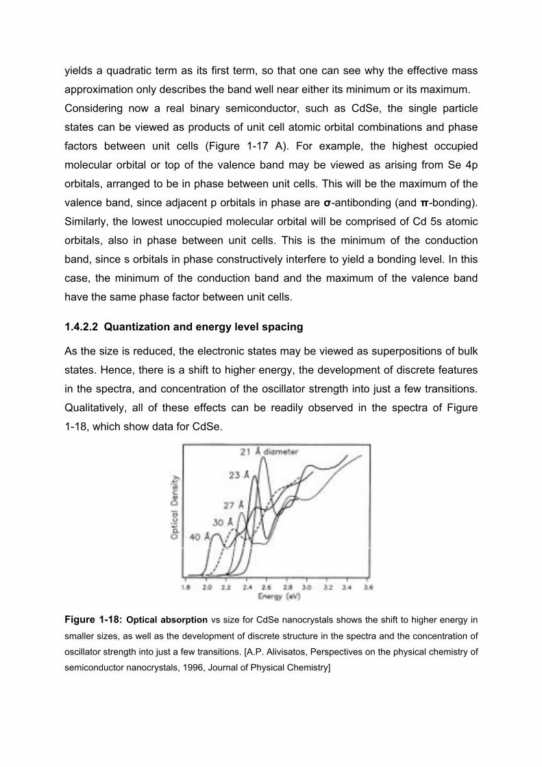
Qualitatively, all of these effects can be readily observed in the spectra of Figure
1-18, which show data for CdSe.
Figure 1-18: Optical absorption vs size for CdSe nanocrystals shows the shift to higher energy in
smaller sizes, as well as the development of discrete structure in the spectra and the concentration of
oscillator strength into just a few transitions. [A.P. Alivisatos, Perspectives on the physical chemistry of
semiconductor nanocrystals, 1996, Journal of Physical Chemistry]
The quantitative analysis of these spectra remains a difficult subject, for several
reasons:
• The foregoing picture is a single-particle one and does not include the
substantial effects of correlation. In molecules this is analogous to trying to use
the highly approximate molecular orbital theory, instead of more advanced
quantum chemistry methods. Regrettably, the nanocrystals are too large to
describe using even moderately advanced methods that are routinely applied
to small molecules.
• Further, in CdSe at least, the large atomic number of the Se ensures that the
coupling between spin and orbital momenta is very strong in the valence
bands (p bands). This coupling is in the j-j, and not the Russell-Saunders, L-S,
coupling regime. When translational symmetry is removed, the mixing of k
vectors can also result in different bands mixing together.
• The shape of the crystallites, which is regular (tetrahedral, hexagonal prisms),
or spherical, or ellipsoidal, will determine the symmetry of the nanocrystals
and will influence the relative spacing of the levels.
• Finally, surface energy levels are completely excluded from this simple
quantum confinement picture. Yet it seems apparent that surface states near
the gap can mix with interior levels to a substantial degree, and these effects
may also influence the spacing of the energy levels.
Theoretical approaches that directly include the influence of the surface, as well as
electronic correlation, are being developed rapidly.
1.4.3 Electrical properties
We talk about single-electronics whenever it is possible to control the
movement and position of a single or small number of electrons. To understand how
a single electron can be controlled, one must understand the movement of electric
charge through a conductor. An electric current can flow through the conductor
because some electrons are free to move through the lattice of atomic nuclei. The
current is determined by the charge transferred through the conductor. Surprisingly
this transferred charge can have practically any value, in particular, a fraction of the
charge of a single electron. Hence, it is not quantized.

This, at first glance counterintuitive fact, is a consequence of the displacement
of the electron cloud against the lattice of atoms. This shift can be changed
continuously and thus the transferred charge is a continuous quantity (see left side of
Figure 1-19).
Figure 1-19: The left side shows, that the electron cloud shift against the lattice of atoms is not
quantized. The right side shows an accumulation of electrons at a tunnel junction.
If a tunnel junction interrupts an ordinary conductor, electric charge will move
through the system by both a continuous and discrete process. Since only discrete
electrons can tunnel through junctions, charge will accumulate at the surface of the
electrode against the isolating layer, until a high enough bias has built up across the
tunnel junction (see right side of Figure 1-19). Then one electron will be transferred.
Likharev has coined the term `dripping tap' as an analogy of this process. In other
words, if a single tunnel junction is biased with a constant current I, the so called
Coulomb oscillations will appear with frequency f = I/e, where e is the charge of an
electron (see Figure 1-20).
Figure 1-20: Current biased tunnel junction showing Coulomb oscillations.
+ + + + + +- - - - - -
+ + + + + +- - - - - -
+ + + + + +- - - - - -
+ + +
+
+++
+ +
+ + +
+
+++
+ +
tunn
el ju
nctio
n
I
I
conduction current
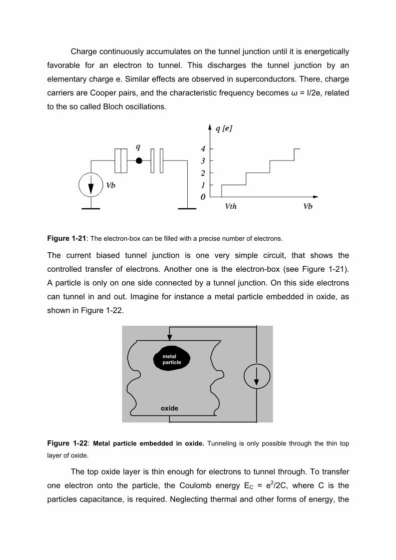
Charge continuously accumulates on the tunnel junction until it is energetically
favorable for an electron to tunnel. This discharges the tunnel junction by an
elementary charge e. Similar effects are observed in superconductors. There, charge
carriers are Cooper pairs, and the characteristic frequency becomes ω = I/2e, related
to the so called Bloch oscillations.
Figure 1-21: The electron-box can be filled with a precise number of electrons.
The current biased tunnel junction is one very simple circuit, that shows the
controlled transfer of electrons. Another one is the electron-box (see Figure 1-21).
A particle is only on one side connected by a tunnel junction. On this side electrons
can tunnel in and out. Imagine for instance a metal particle embedded in oxide, as
shown in Figure 1-22.
Figure 1-22: Metal particle embedded in oxide. Tunneling is only possible through the thin top
layer of oxide.
The top oxide layer is thin enough for electrons to tunnel through. To transfer
one electron onto the particle, the Coulomb energy EC = e2/2C, where C is the
particles capacitance, is required. Neglecting thermal and other forms of energy, the
oxide
metalparticle
only energy source available is the bias voltage Vb. As long as the bias voltage is
small enough, smaller than a threshold Vth = e/C, no electron can tunnel, because not
enough energy is available to charge the island. This behavior is called the Coulomb
blockade. Raising the bias voltage will populate the particle with one, then two and so
on electrons, leading to a staircase-like characteristic.
It is easily understandable, that these single-electron phenomena, such as Coulomb oscillations and Coulomb blockade, only matter, if the Coulomb energy
is bigger than the thermal energy. Otherwise thermal fluctuations will disturb the
motion of electrons and will wash out the quantization effects. The necessary
condition is,
2
2c BeE k TC
= > (1. 26)
Where kB is Boltzmann's constant and T is the absolute temperature. This means
that the capacitance C has to be smaller than 12 nF for the observation of charging
effects at the temperature of liquid nitrogen and smaller than 3 nF for charging effects
to appear at room temperature. A second condition for the observation of charging
effects is, that quantum fluctuations of the number of electrons on an island must be
negligible. Electrons need to be well localized on the islands. If electrons would not
be localized on islands one would not observe charging effects, since islands would
not be separate particles but rather one big uniform space. The charging of one
island with an integer number of the elementary charge would be impossible,
because one electron is shared by more than one island. The Coulomb blockade
would vanish, since no longer would a lower limit of the charge, an island could be
charged with, exist. This leads to the requirement that all tunnel junctions must be
opaque enough for electrons in order to confine them on islands. The `transparency'
of a tunnel junction is given by its tunnel resistance RT which must fulfill the following
condition for observing discrete charging effects, where h is Planck's constant. This
should be understood as an order-of-magnitude measure, rather than an exact
threshold.
2 25813ThRe
> = Ω (1. 27)
Therefore, these effects are experimentally verifiable only for very small high-
resistance tunnel junctions, meaning small particles with small capacitances and/or
very low temperatures. Advanced fabrication techniques, such as the production of
granular films with particle sizes down to 1 nm, and deeper physical understanding
allow today the study of many charging effects at room temperature.
Based on the Coulomb blockade many interesting devices are possible, such as precise current standard, x very sensitive electrometers, xi logic gates xii and
memories xiii with ultra low power consumption, down-scalability to atomic
dimensions, and high speed of operation. Altogether, single-electronics will bring new
and novel devices and is a very promising candidate to partly replace MOS
technology in the near future.
1.4.4 Optical Properties
1.4.4.1 Line widths: Size distributions and intrinsic broadening
As a consequence of their being a new type of material, the properties of
semiconductor nanocrystals can be expected to evolve with improvements in sample
preparation. Spectra which at first seemed featureless and diffuse have gradually
acquired definition, with multiple discrete states apparent in the latest generation of
samples. Essentially all of this progress derives from narrowing the distribution of
sizes in the sample. Since the energies of the transitions depend so strongly on the
size, size variation is a special form of inhomogeneous broadening at work here,
which over time has been largely reduced. Today it is really the intrinsic, or single
particle, line widths that are a matter of greater concern.
ILuminescence and electroluminescence
Narrow band (15-20 nm), size-tunable luminescence, with efficiencies at least of
order 10%, is observed at room temperature from semiconductor nanocrystals. The
origin of this luminescence remains the topic of some controversy. For some time
researchers thought that this luminescence arose from partially surface trapped
carriers. Other experiments strongly suggest that the luminescence in fact arises
from low-lying “dark” states of the nanocrystal interior, and surface modifications only
influence the quantum yield by modulating the non radiative rates. Just as in organic
molecules a singlet state may be optically prepared, followed by rapid relaxation to
triplet states with long decay times, so in semiconductor nanocrystals, where j-j coupling dominates, an angular momentum allowed state is initially prepared, and on
the time scale of picoseconds or longer, there is a decay to a lower lying angular-
momentum-forbidden state, which decays relatively slowly (nanoseconds to
microseconds). One success of this dark state model is the accurate prediction that
the magnitude of the exchange splitting increases as r-3, thus explaining one long
puzzling feature of the luminescence. As the size is reduced, the shift between the
absorbing and emitting state is observed to increase. The rigorous separation of
interior and surface states is somewhat artificial in nanocrystals in any case, since
substantial mixing may be expected. Indeed, other features of the spectra suggest
that there may well be substantial surface character associated with the emitting
state. For example, electric field modulation of the luminescence yields signals a
factor of 100 or larger than modulation of absorption, indicating that the emitting state
is not as well confined spatially. Further evidence for surface localization of the
emitting state comes from low-temperature studies of the vibronic coupling of the
emission, which show that there is a well-defined localization temperature.
Independent of the exact origin of the luminescence, it does appear to be one
property which can be manipulated in useful ways. For example, two reports of light-
emitting diodes made with polymers and CdSe nanocrystals have appeared within
the past year. In the first instance, nanocrystals were assembled in layers a few
nanocrystals thick on the surface of PPV, an electroluminescent polymer. The PPV
itself was grown on a layer of indium tin oxide, a transparent hole-injecting contact.
Finally, the nanocrystal layer was coated with a film of Mg/Ag, the electron-injecting
contact. This complete assembly electroluminesces when a voltage is applied. The
recombination of electrons and holes may take place either in the polymer layer
(which emits green light) or in the nanocrystal layer. The nanocrystal emission shifts
with size. Thus, these LEDs provide a variety of means for tuning the output color.
This advance is particularly important, since it constitutes the first example of
electrical, rather than purely optical, investigation of semiconductor nanocrystals.
References:
[1] A.P. Alivisatos, Perspectives on the physical chemistry of semiconductor
nanocrystals, 1996, Journal of Physical Chemistry
[2] S. Ciraci, A. Buldum, I.P. Batra, Quantum effects in electrical and thermal
transport through nanowires, 2001, Journal of Physics Condensed Matter

[3] S. Eustis, M. A. El-Sayed, Why gold nanoparticles are more precious than pretty
gold: Noble metal surface plasmon resonance and its enhancement of the radiative
and nonradiative properties of nanocrystals of different shapes, 2005, The royal
Society of Chemistry
[4] K. Lance Kelly, E. Coronado, L.L. Zhao, G.C. Schatz, The Optical Properties of
Metal Nanoparticles: The Influence of Size, Shape, and Dielectric Environment, 2003,
Journal of Physical Chemistry
i Marquardt, P.;Börngen, L.;Nimtz, G.;Gleiter, R.;Sonneberger, R., Zhu, J., Phys. Lett. 1986, 114 , 39. ii Henglein, A., Chem. Rev. 1989, 89 , 1861. iii G. Schön, G., Simon, U., Colloid Polym. Sci. 1995, 273 , 101. iv Weller, H., Eychmüller, A. Semiconductor Nanoclusters; Elsevier Science; Amsterdam, 1996. v Weller, H., Adv. Mater. 1993, 5 , 2, 88. vi G. Schön, G., Simon, U., Colloid Polym. Sci. 1995, 273 , 202. vii U. Simon, U.;Schön, G., Schmid, G., Angew. Chem. Int. Ed. Engl. 1993, 232 , 250. viii Schmid, G., Chem. Rev. 1992, 92 , 1709. ix Schmid, G.;Pfeil, R.;Boese, R.;Bandermann, F.;Mayer, S.;Calis, G. H. M., Van der Velden, J. W. A.,
Chem. Ber. 1981, 114 , 3634. x J. M. Martinis, M. Nahum, and H. D. Jensen, Physical Review Letters, 72, (1994) 904. xi A. N. Korotkov, D. V. Averin, K. K. Likharev, and S. A. Vasenko, In H. Koch and H. Lübbig, editors,
Single-Electron Tunneling and Mesoscopic Devices, pages 45-59. Springer-Verlag, Berlin Heidelberg
New York, 1992. xii P. D. Tougaw and C. S. Lent, Journal of Applied Physics, 75 (1994)1818; J. R. Tucker, J. Appl.
Phys., 72 (1992) 4399. xiii K. Nakazato, R. J. Blaikie, and H. Ahmed, J. Appl. Phys., 75 (1994) 5123; K. Yano, T. Ishii, T. Sano,
T. Mine, F. Murai, and K. Seki, IEEE International Solid-State Circuits Conference, pages 266-267,
1996.