Lect2 CMOS Process - Yonsei Universitytera.yonsei.ac.kr/class/2013_1/lecture/Lect3 CMOS...
28
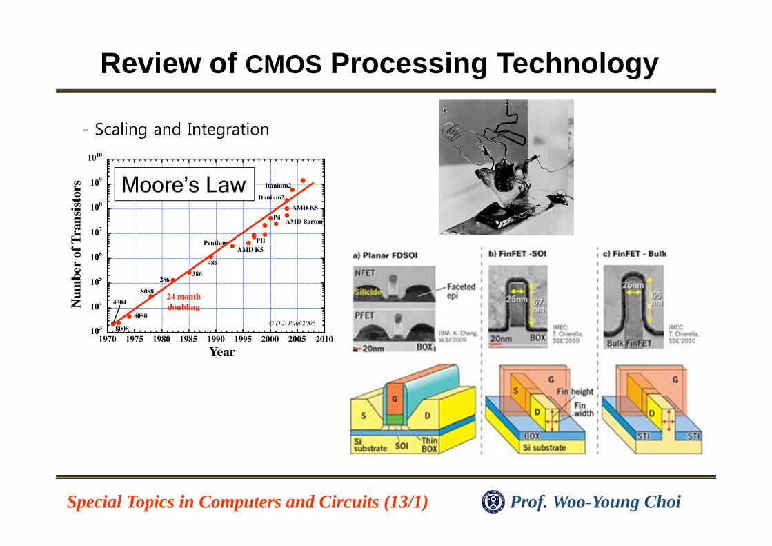
Review of CMOS Processing Technology Prof. Woo-Young Choi Special Topics in Computers and Circuits (13/1) - Scaling and Integration Moore’s Law
Transcript of Lect2 CMOS Process - Yonsei Universitytera.yonsei.ac.kr/class/2013_1/lecture/Lect3 CMOS...
Review of CMOS Processing Technology
Prof. Woo-Young ChoiSpecial Topics in Computers and Circuits (13/1)
- Scaling and Integration
Moore’s Law
Review of CMOS Processing Technology
Prof. Woo-Young ChoiSpecial Topics in Computers and Circuits (13/1)
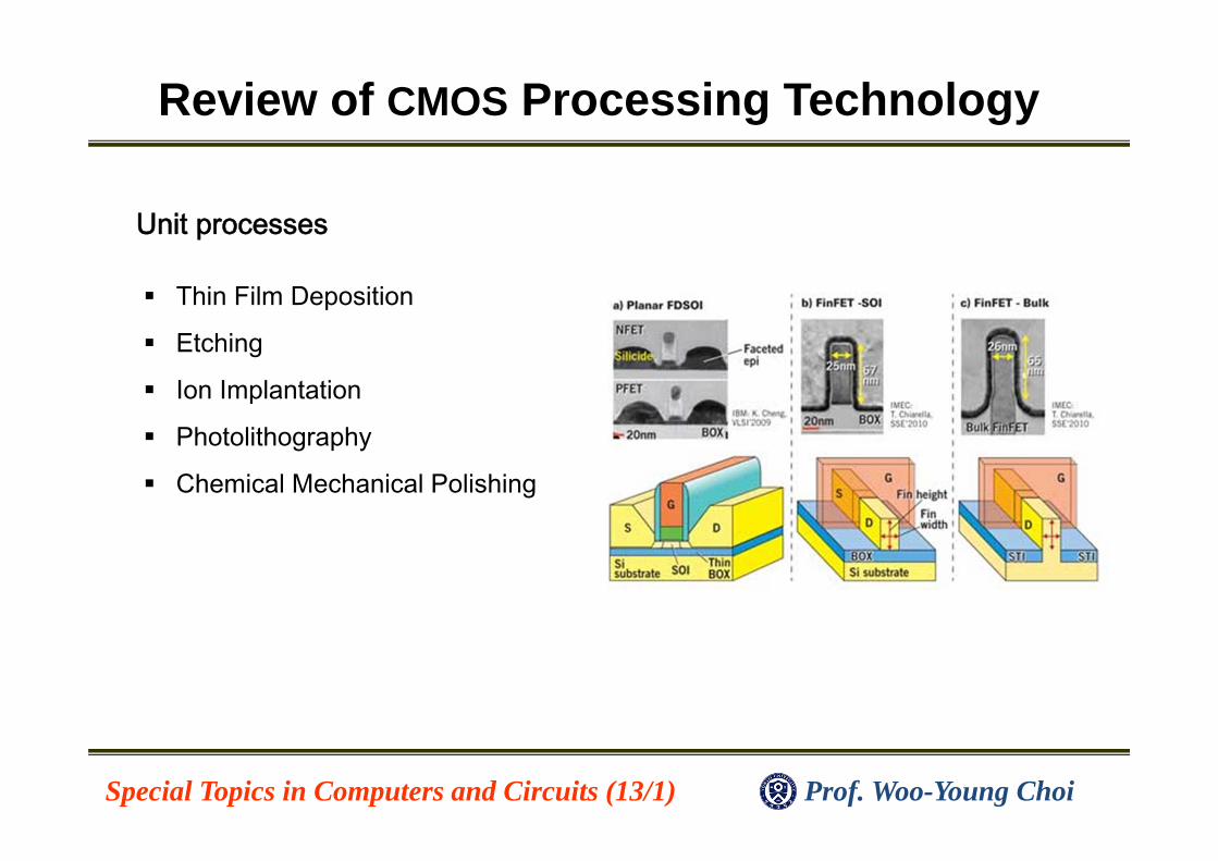
Unit processes
Thin Film Deposition
Etching
Ion Implantation
Photolithography
Chemical Mechanical Polishing
Review of CMOS Processing Technology
Prof. Woo-Young ChoiSpecial Topics in Computers and Circuits (13/1)
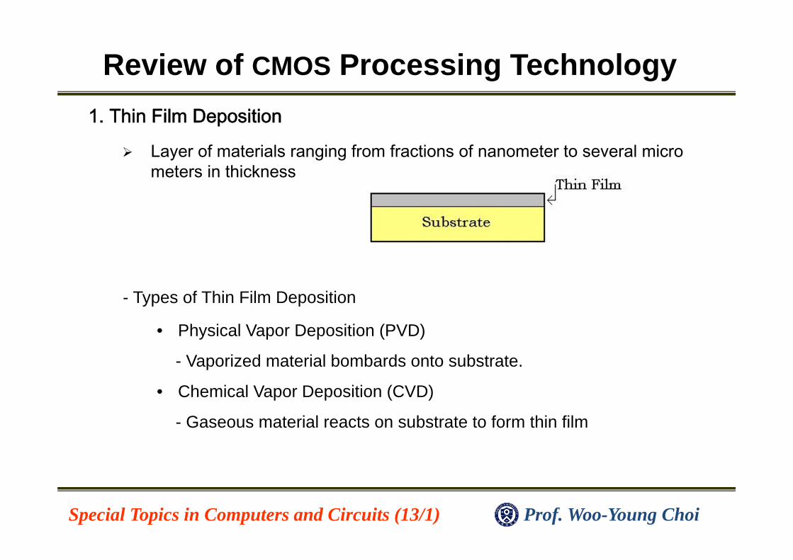
1. Thin Film Deposition
Layer of materials ranging from fractions of nanometer to several micro meters in thickness
- Types of Thin Film Deposition
• Physical Vapor Deposition (PVD)
- Vaporized material bombards onto substrate.
• Chemical Vapor Deposition (CVD)
- Gaseous material reacts on substrate to form thin film
Review of CMOS Processing Technology
Prof. Woo-Young ChoiSpecial Topics in Computers and Circuits (13/1)
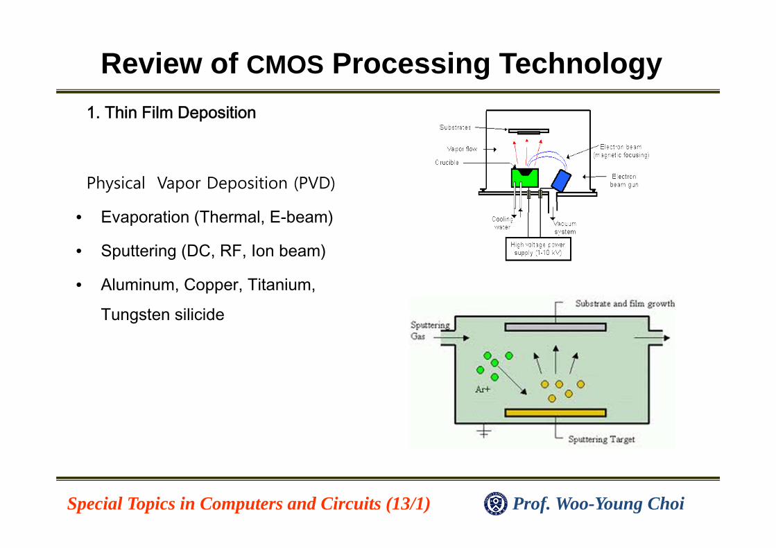
• Evaporation (Thermal, E-beam)
• Sputtering (DC, RF, Ion beam)
• Aluminum, Copper, Titanium,
Tungsten silicide
Physical Vapor Deposition (PVD)
1. Thin Film Deposition
Review of CMOS Processing Technology
Prof. Woo-Young ChoiSpecial Topics in Computers and Circuits (13/1)
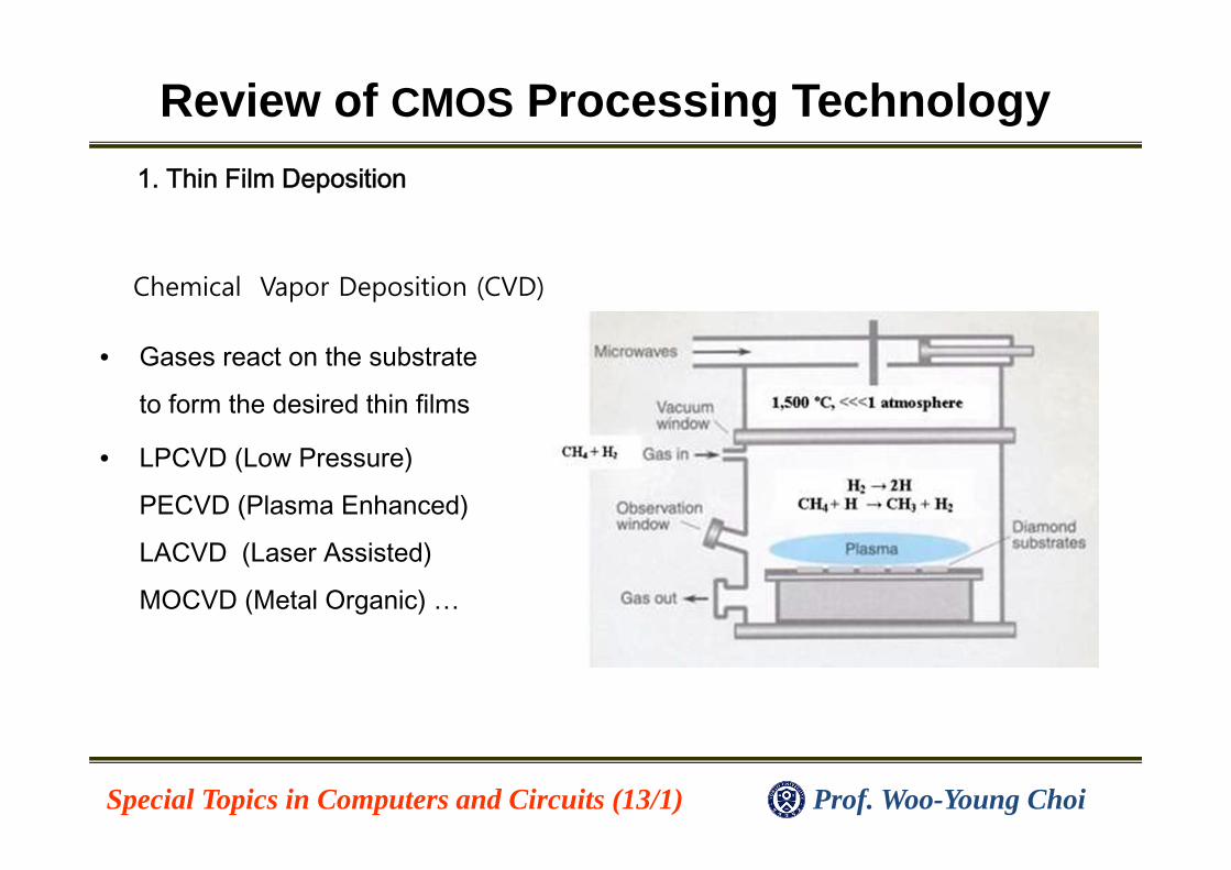
Chemical Vapor Deposition (CVD)
• Gases react on the substrate
to form the desired thin films
• LPCVD (Low Pressure)
PECVD (Plasma Enhanced)
LACVD (Laser Assisted)
MOCVD (Metal Organic) …
1. Thin Film Deposition
Review of CMOS Processing Technology
Prof. Woo-Young ChoiSpecial Topics in Computers and Circuits (13/1)
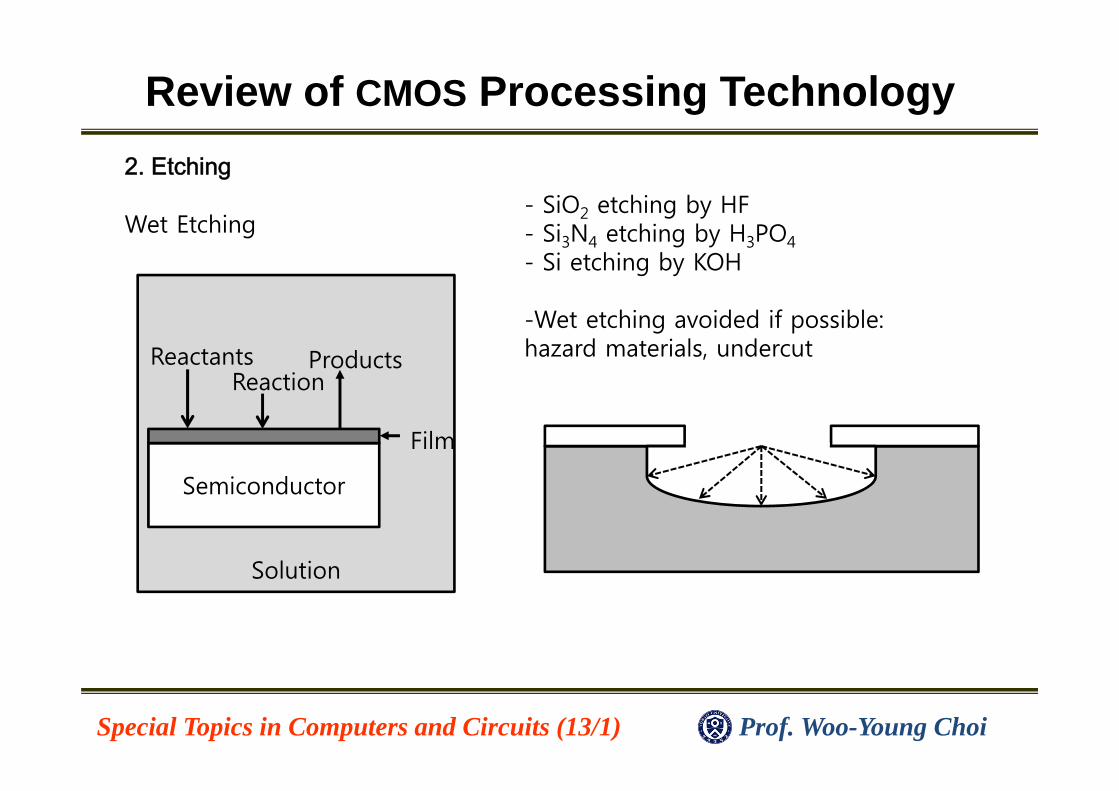
- SiO2 etching by HF- Si3N4 etching by H3PO4- Si etching by KOH
-Wet etching avoided if possible: hazard materials, undercut
2. Etching
Wet Etching
Semiconductor
Solution
Film
ProductsReaction
Reactants
Review of CMOS Processing Technology
Prof. Woo-Young ChoiSpecial Topics in Computers and Circuits (13/1)
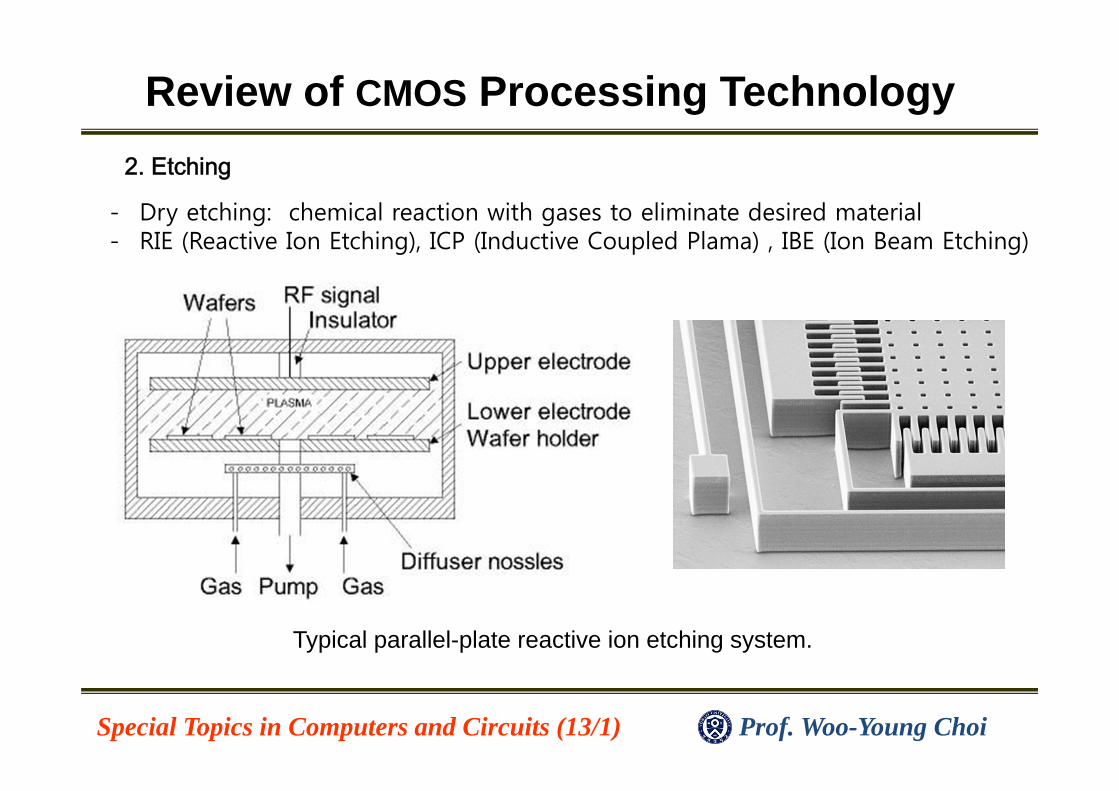
2. Etching
- Dry etching: chemical reaction with gases to eliminate desired material- RIE (Reactive Ion Etching), ICP (Inductive Coupled Plama) , IBE (Ion Beam Etching)
Typical parallel-plate reactive ion etching system.
Review of CMOS Processing Technology
Prof. Woo-Young ChoiSpecial Topics in Computers and Circuits (13/1)
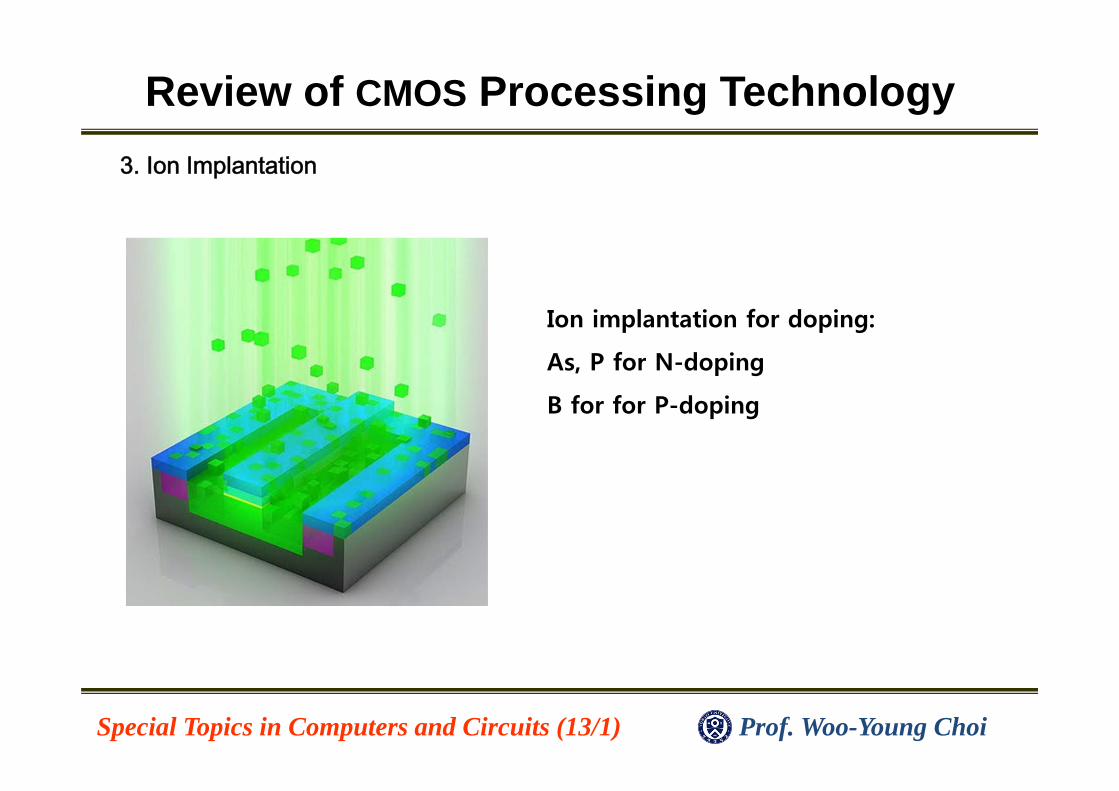
3. Ion Implantation
Ion implantation for doping:
As, P for N-doping
B for for P-doping
Review of CMOS Processing Technology
Prof. Woo-Young ChoiSpecial Topics in Computers and Circuits (13/1)
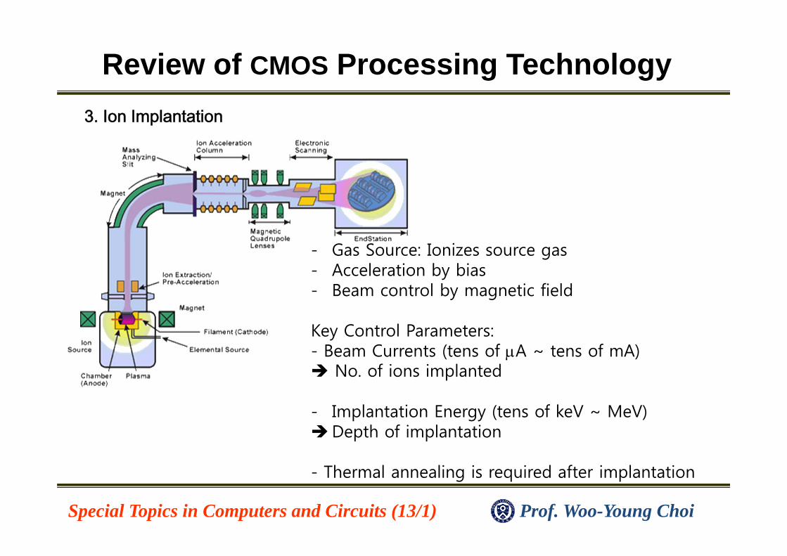
3. Ion Implantation
- Gas Source: Ionizes source gas- Acceleration by bias- Beam control by magnetic field
Key Control Parameters: - Beam Currents (tens of A ~ tens of mA) No. of ions implanted
- Implantation Energy (tens of keV ~ MeV)Depth of implantation
- Thermal annealing is required after implantation
Review of CMOS Processing Technology
Prof. Woo-Young ChoiSpecial Topics in Computers and Circuits (13/1)
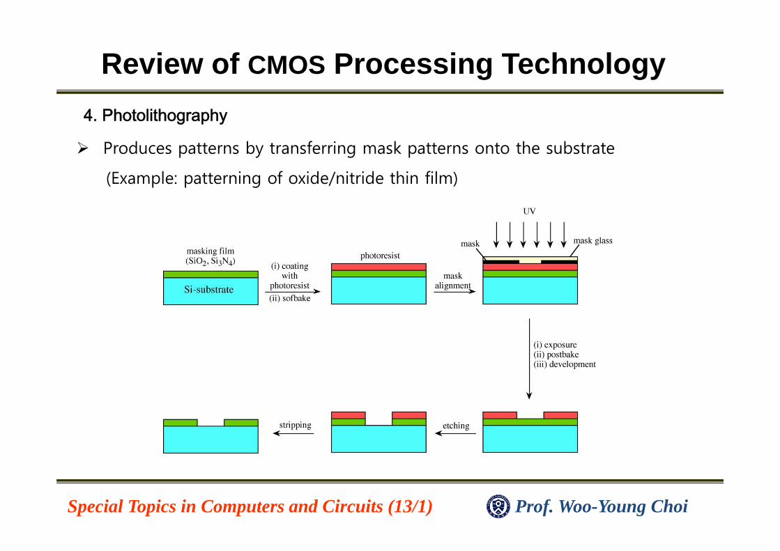
Produces patterns by transferring mask patterns onto the substrate
(Example: patterning of oxide/nitride thin film)
4. Photolithography
Review of CMOS Processing Technology
Prof. Woo-Young ChoiSpecial Topics in Computers and Circuits (13/1)
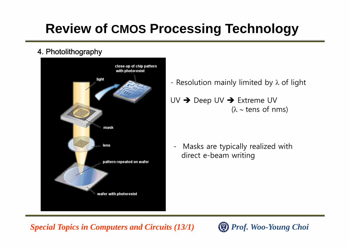
4. Photolithography
- Resolution mainly limited by of light
UV Deep UV Extreme UV (tens of nms)
- Masks are typically realized withdirect e-beam writing
Review of CMOS Processing Technology
Prof. Woo-Young ChoiSpecial Topics in Computers and Circuits (13/1)
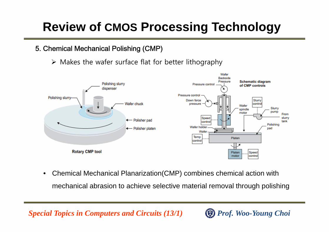
5. Chemical Mechanical Polishing (CMP)
Makes the wafer surface flat for better lithography
• Chemical Mechanical Planarization(CMP) combines chemical action with
mechanical abrasion to achieve selective material removal through polishing
Review of CMOS Processing Technology
Prof. Woo-Young ChoiSpecial Topics in Computers and Circuits (13/1)
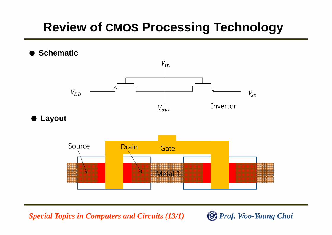
Metal 1
GateSource Drain
Invertor
Schematic●
Layout●
Review of CMOS Processing Technology
Prof. Woo-Young ChoiSpecial Topics in Computers and Circuits (13/1)
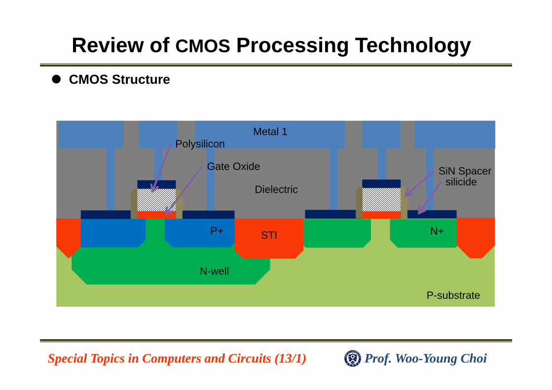
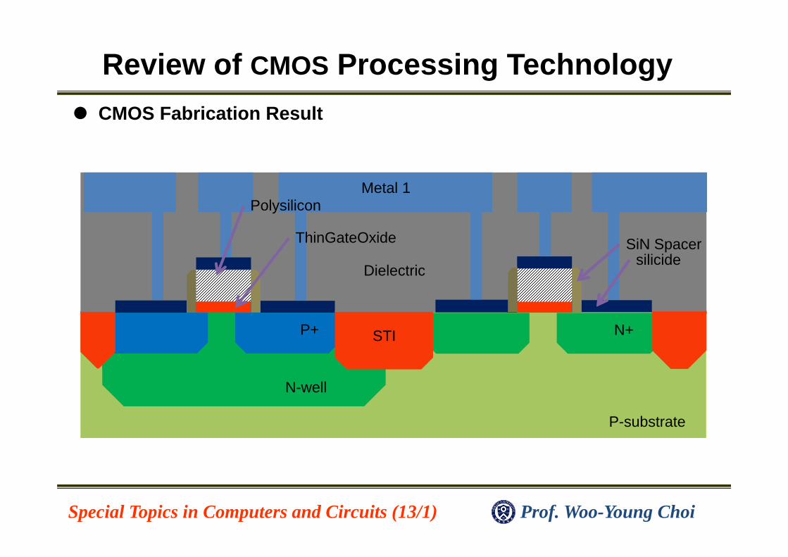
P-substrate
N-well
SiN Spacersilicide
Metal 1
Dielectric
P+ N+STI
Gate Oxide
Polysilicon
CMOS Structure●
Review of CMOS Processing Technology
Prof. Woo-Young ChoiSpecial Topics in Computers and Circuits (13/1)
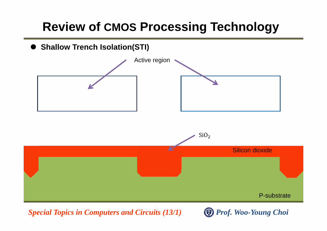
Active region
SiO
Shallow Trench Isolation(STI)
Silicon dioxide
●
P-substrate
Review of CMOS Processing Technology
Prof. Woo-Young ChoiSpecial Topics in Computers and Circuits (13/1)
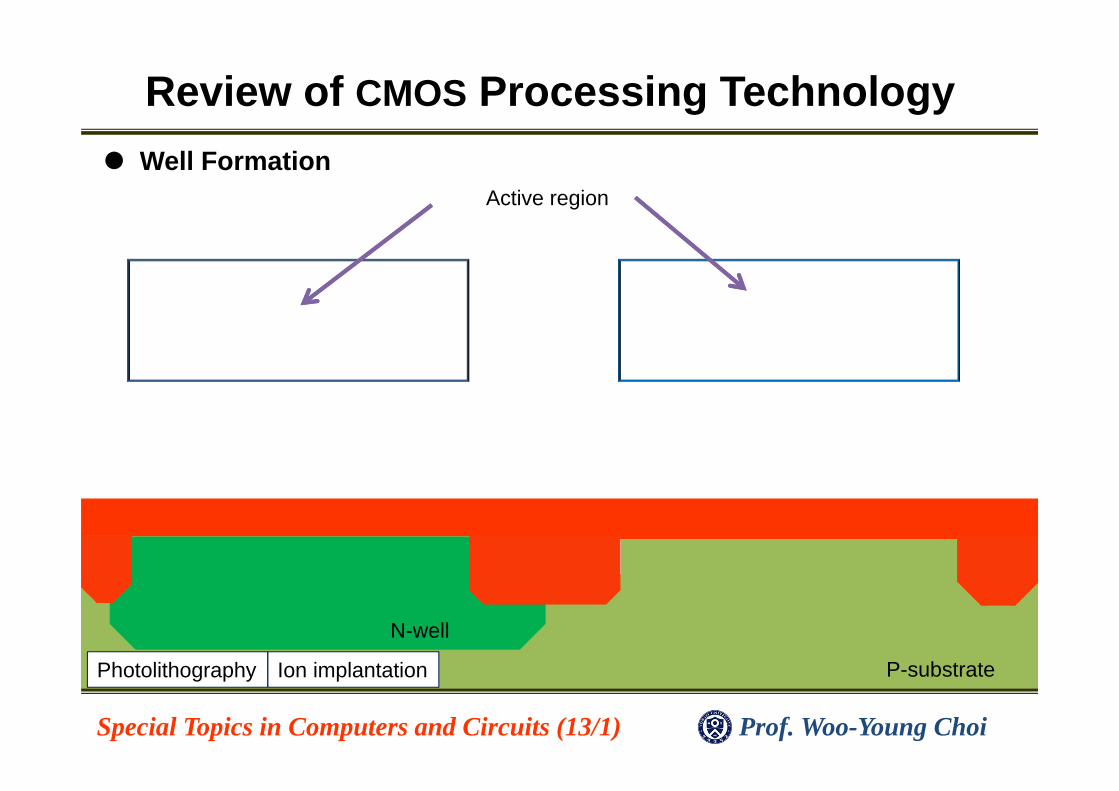
Well Formation●
P-substrate
N-well
Active region
Photolithography Ion implantation
Review of CMOS Processing Technology
Prof. Woo-Young ChoiSpecial Topics in Computers and Circuits (13/1)
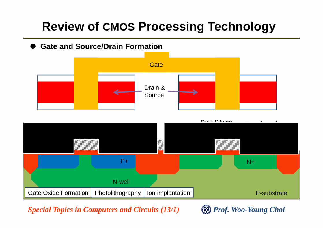
Gate
Drain &Source
Poly Silicon Thin Gate Oxide
N+P+
P-substrate
N-well
Gate and Source/Drain Formation●
Gate Oxide Formation Photolithography Ion implantation
Review of CMOS Processing Technology
Prof. Woo-Young ChoiSpecial Topics in Computers and Circuits (13/1)
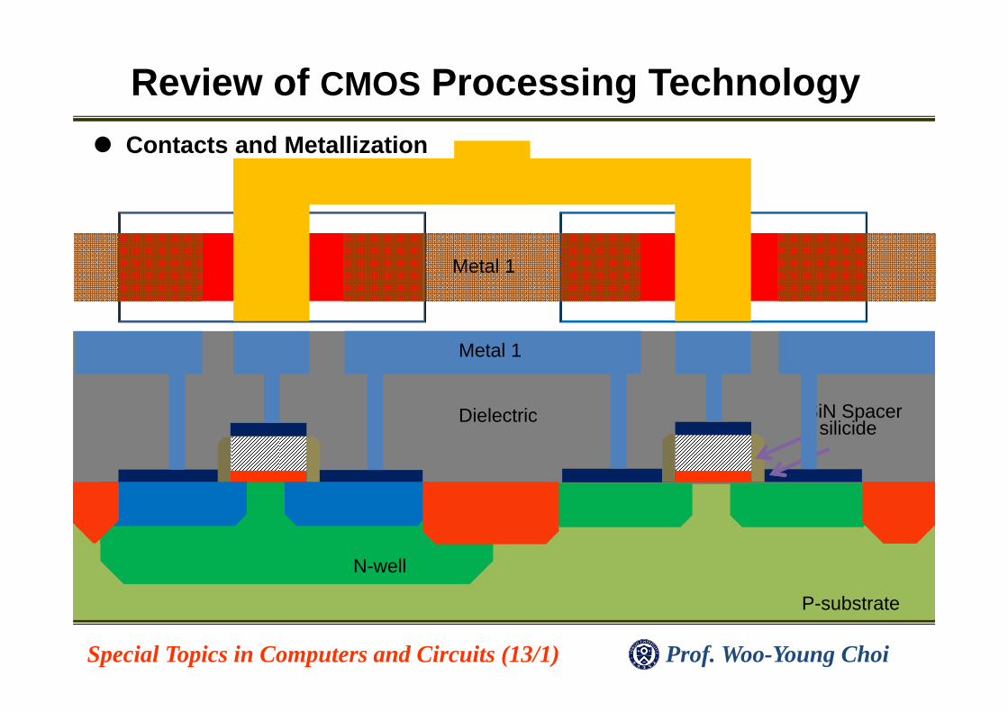
P-substrate
N-well
Metal 1
SiN Spacersilicide
Metal 1
Dielectric
Contacts and Metallization●
Review of CMOS Processing Technology
Prof. Woo-Young ChoiSpecial Topics in Computers and Circuits (13/1)
P-substrate
N-well
SiN Spacersilicide
Metal 1
Dielectric
P+ N+STI
ThinGateOxide
Polysilicon
CMOS Fabrication Result●
Review of CMOS Processing Technology
Prof. Woo-Young ChoiSpecial Topics in Computers and Circuits (13/1)
- CMOS Circuit Design Process
Review of CMOS Processing Technology
Prof. Woo-Young ChoiSpecial Topics in Computers and Circuits (13/1)
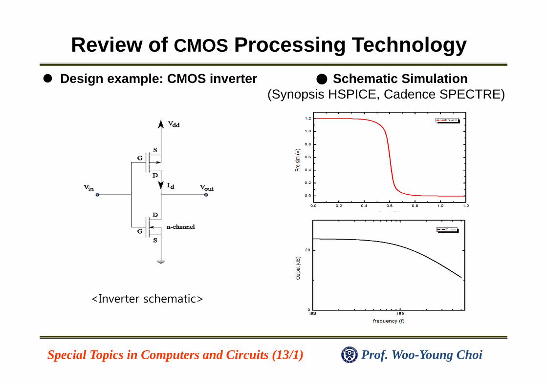
Design example: CMOS inverter●
<Inverter schematic>
● Schematic Simulation(Synopsis HSPICE, Cadence SPECTRE)
Review of CMOS Processing Technology
Prof. Woo-Young ChoiSpecial Topics in Computers and Circuits (13/1)
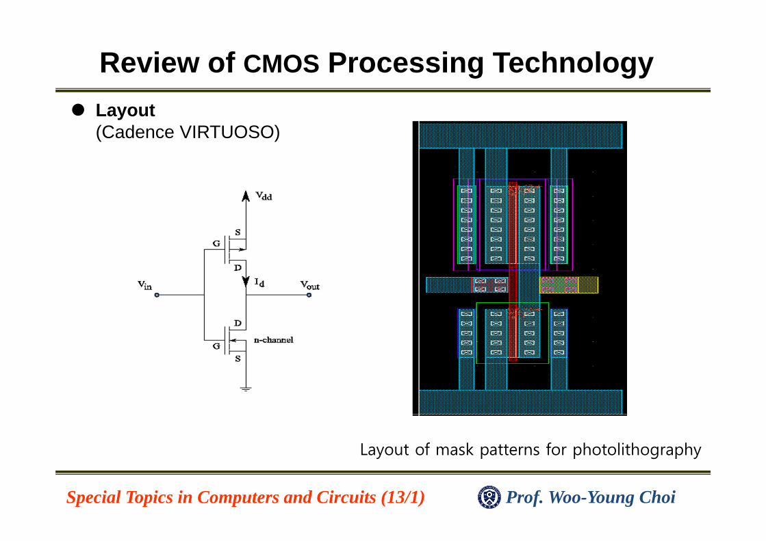
● Layout(Cadence VIRTUOSO)
Layout of mask patterns for photolithography
Review of CMOS Processing Technology
Prof. Woo-Young ChoiSpecial Topics in Computers and Circuits (13/1)
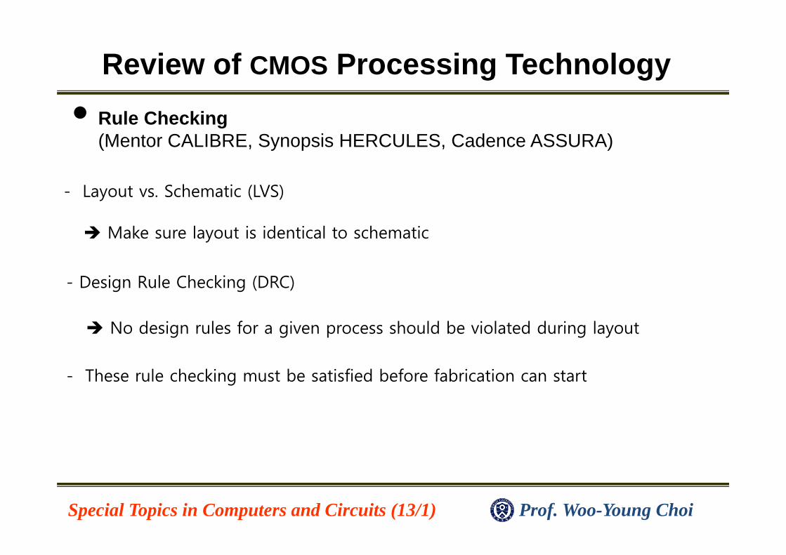
● Rule Checking (Mentor CALIBRE, Synopsis HERCULES, Cadence ASSURA)
- Design Rule Checking (DRC)
No design rules for a given process should be violated during layout
- These rule checking must be satisfied before fabrication can start
- Layout vs. Schematic (LVS)
Make sure layout is identical to schematic
Review of CMOS Processing Technology
Prof. Woo-Young ChoiSpecial Topics in Computers and Circuits (13/1)
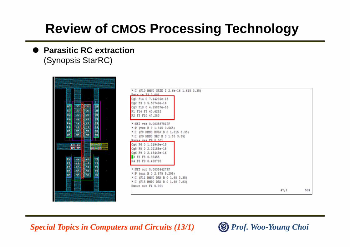
● Parasitic RC extraction(Synopsis StarRC)
Review of CMOS Processing Technology
Prof. Woo-Young ChoiSpecial Topics in Computers and Circuits (13/1)
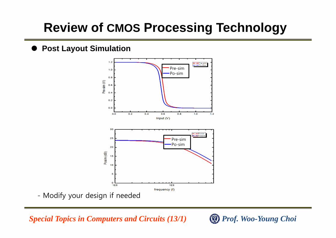
● Post Layout Simulation
Pre-simPo-sim
Pre-simPo-sim
- Modify your design if needed
Review of CMOS Processing Technology
Prof. Woo-Young ChoiSpecial Topics in Computers and Circuits (13/1)
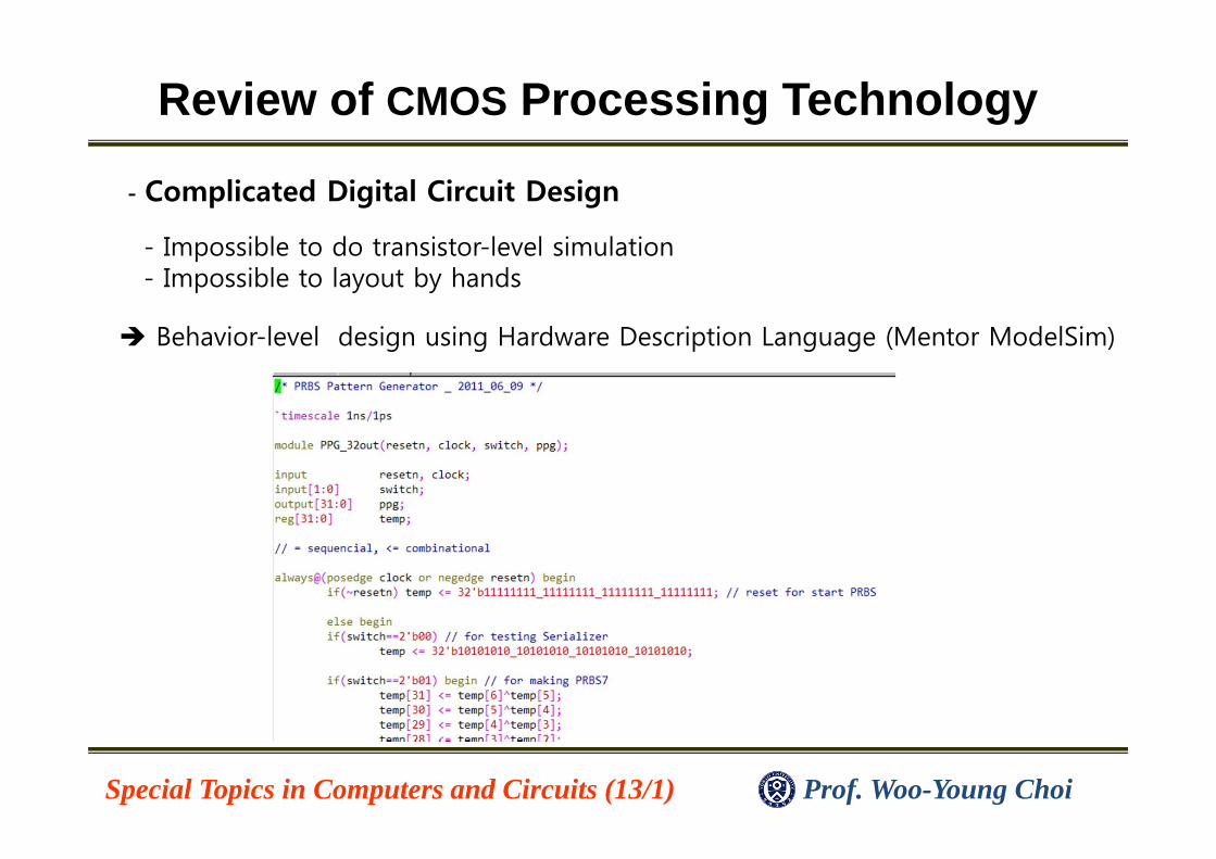
- Complicated Digital Circuit Design
- Impossible to do transistor-level simulation- Impossible to layout by hands
Behavior-level design using Hardware Description Language (Mentor ModelSim)
Review of CMOS Processing Technology
Prof. Woo-Young ChoiSpecial Topics in Computers and Circuits (13/1)
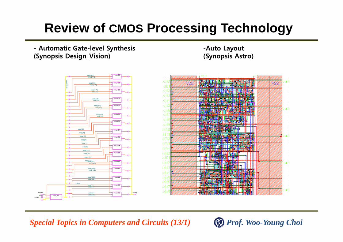
- Automatic Gate-level Synthesis (Synopsis Design_Vision)
-Auto Layout(Synopsis Astro)
Review of CMOS Processing Technology
Prof. Woo-Young ChoiSpecial Topics in Computers and Circuits (13/1)
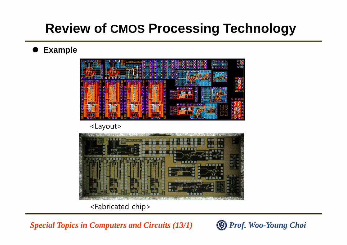
● Example
<Layout>
<Fabricated chip>