law, Stefan-Boltzmann law. Factors affecting the limiting ...
37
What we learnt last lecture: • Black body radiation: Planck’s law, Wien’s displacement law, Stefan-Boltzmann law. • Light source. AM1.5 • Solar cell in dark and under illumination. • Factors affecting the limiting efficiency: Band gap and spectrum. Shockley-Queisser limit • Requirements for an ideal solar cell. Solar cell Ambient radiation Spontaneous emission Solar radiation Spontaneous emission 1
Transcript of law, Stefan-Boltzmann law. Factors affecting the limiting ...

What we learnt last lecture:
• Black body radiation: Planck’s law, Wien’s displacement law, Stefan-Boltzmann law.
• Light source. AM1.5• Solar cell in dark and under illumination.• Factors affecting the limiting efficiency: Band gap and
spectrum. Shockley-Queisser limit• Requirements for an ideal solar cell.
Solar cell
Ambient radiation
Spontaneous emission
Solar radiation
Spontaneous emission
1

Electrons and Holes in Semiconductor
Lecture 3
References:1. Physics of Solar Cells. Jenny Nelson. Imperial College Press, 2003.2. Photovoltaic Materials, Series on Properties of Semiconductor
Materials, Vol.1, Richard H. Bube, Imperial College Press, 1998.3. Third Generation Photovoltaics: Advanced Solar Energy Conversion.
Martin A. Green, Springer, 2006.4. Wikipedia (http://en.wikipedia.org/wiki/Main_Page).
2

1. Why Semiconductors?2. Semiconductor in Equilibrium3. Semiconductor under Bias
3

Why Semiconductors?
• Metal, Semimetal, Semiconductor, Insulator• Band Gap• Conduction Band and Valence Band• Charge Carriers: Electron and Hole• Exciton • Photoconductivity• Band Structure• Density of State (DOS)
4

Why Semiconductors?
Requirements for a suitable photovoltaic material: (1) absorb visible light, (2) possess a band gap for photon absorption and charge separation,(3) be able to transport charges efficiently.
Semiconductors: Band Gap enables excited electrons to remain in higher energy levels for long enough to be exploited.
fs
fs
µs
Conduction band
Metal Semiconductor Insulator
Fermi Level
Valence band
Ban
dgapOverlap
5

Bonds and Bands in Crystals
1 2 N Crystal 1 2 N Crystal
Metal Semiconductor or InsulatorEn
ergy
band gap
Conduction band
Valence band
Molecular orbitalHOMO & LUMO
BandConduction band & Valence band
Atomic orbital
Valence Band (VB): The highest occupied band, contains the valence electrons.Conduction Band (CB): The lowest unoccupied band.
6

Semiconductor: VB is completely full and separated from the CB by an energy gap of 0.5~4 eV. All valence electrons in VB are involved in bonding and cannot be easily removed. Not a good heat and electric conductor.Insulator: VB is completely full and separated from the CB by a large energy gap. Negligible conductivity at room temperature.Semimetal: A small overlap in the energy of the CB and VB. However, the bottom of the conduction band is typically situated in a different part of momentum space. Unlike metal, it has two types of charge carriers.
Bonds and Bands in Crystals
Metal: VB is partly full or overlaps with CB. Valence electron is easy to be excited, scattered into a neighboring state in the presence of empty states at similar energies. Good heat and electric conductor.
7

Electrons, Holes and Conductivity
The dynamics of the holes are equivalent to those of a particle with the opposite charge, wavevector and energetics to the missing electron.
CB
VBhole
electron
CB
VBT=0
CB
VBT>0
The vacancy can be filled by another electron involved in neighboring bonds. Then the vacancy moves to the neighboring bond.
8

Semiconductor and Photoconductivity
Two classic examples of photoconductors: photocopying (xerography) and infrared detection applications.
Photoconductivity: an optical and electrical phenomenon in which a material becomes more conductive due to the absorption of electro-magnetic radiation.
hν > Eg
CB
VB
Eg
e-
h+
9

Excitons
Exciton: a bound state of an electron and an imaginary particle hole in an insulator or semiconductor, and is a Coulomb-correlated electron-hole pair. It is an elementary excitation, or a quasiparticle of a solid. Excitons provide a means to transport energy without transporting net charge. The excitons must be split before doing work.
Exciton levels Eg
Valence band
Conduction band
-
+
Coulombic interaction
10

Electron States in Semiconductors
Band Structure Diagram: The map of energies E against wavevector k for the two or three most important directions in the crystal.
Energy levels of atom/molecule can be obtained by solving Schrödinger’s equation. The electron states in crystalline material with infinite periodic lattice structure can be described by Bloch wavefunction.
Band gap
Ener
gy, E
Wavevector, k
Valence band
Conduction band
<110> <000> <100>
Brillouin zone boundary
11

Parabolic band approximation: If k is near a central minimum of a band, it is possible to approximate the energy (band) E(k) with a parabola.
€
E k( ) = EC 0 +h2 k − kC 0
2
2mC*
mC* and mV* are effective mass of electron and hole, and
Electron States in Semiconductors
€
E k( ) = EV 0 −h2 k − kV 0
2
2mV*
€
1mC* =
1h2∂ 2EC k( )∂k 2
€
1mV* = −
1h2∂ 2EV k( )∂k 2
Band gap
Ener
gy, E
Wavevector, k<110> <000> <100>
12

Direct and Indirect Band Gaps
Fundamental band gap (Eg): The minimum amount of energy promoting an electron from the valence band (VB) into the conduction band (CB).Direct band gap: The CB minimum and VB maximum occur at the same value of k.Indirect band gap: The CB minimum and VB maximum occur at different values of k. The phonon gives up its momentum to the electron at the moment of photon absorption so that both energy and momentum are conserved.
13
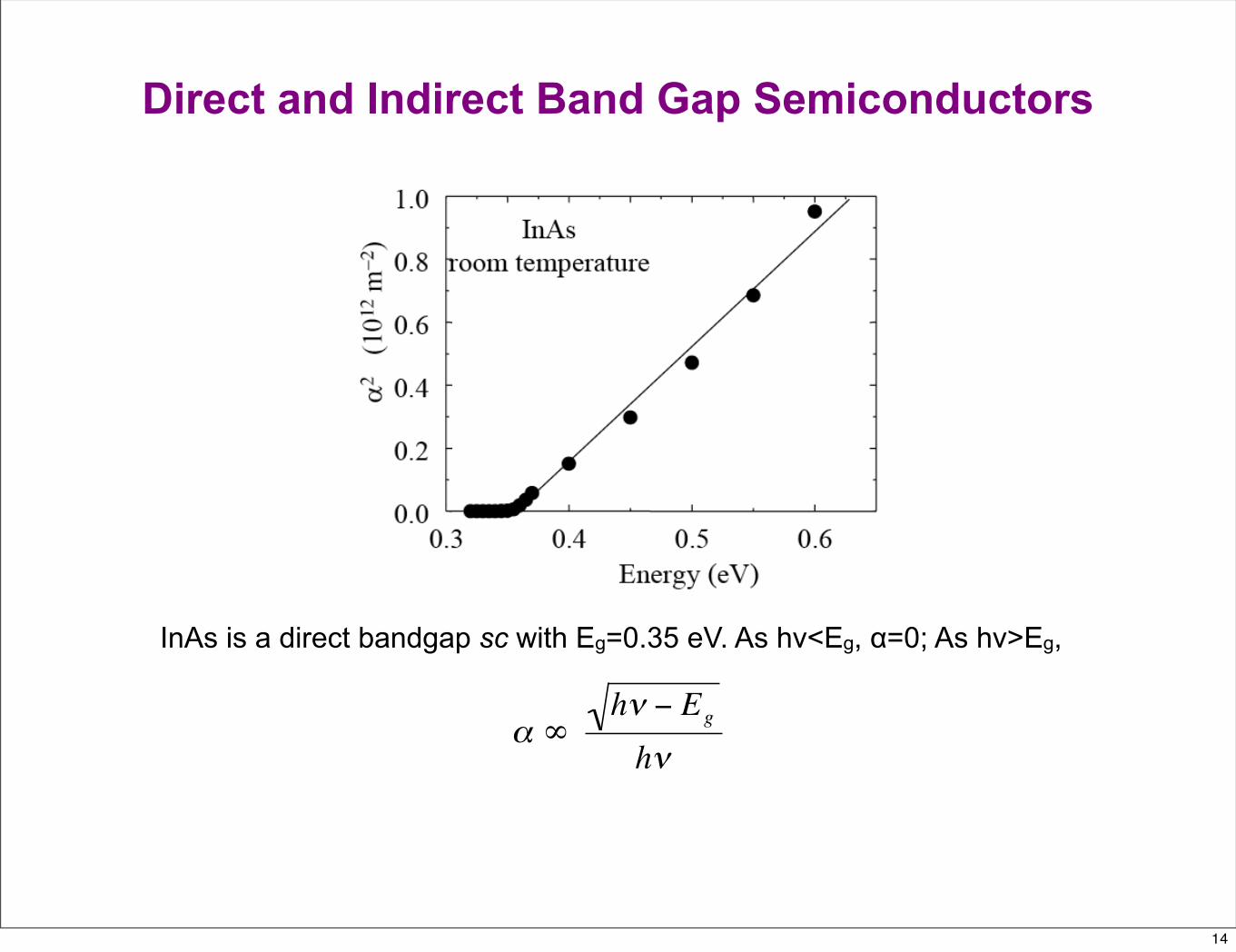
Direct and Indirect Band Gap Semiconductors
€
α ∞hν − Eg
hν
InAs is a direct bandgap sc with Eg=0.35 eV. As hν<Eg, α=0; As hν>Eg,
14
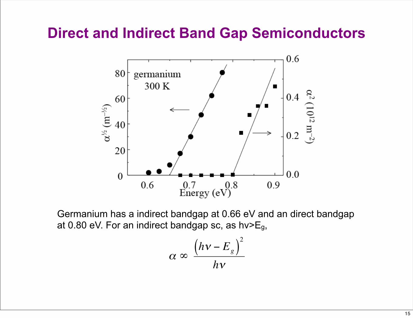
€
α ∞hν − Eg( )
2
hν
Germanium has a indirect bandgap at 0.66 eV and an direct bandgap at 0.80 eV. For an indirect bandgap sc, as hν>Eg,
Direct and Indirect Band Gap Semiconductors
15

Direct and Indirect Band Gap Semiconductors
Direct absorption is much stronger than the indirect absorption.
16
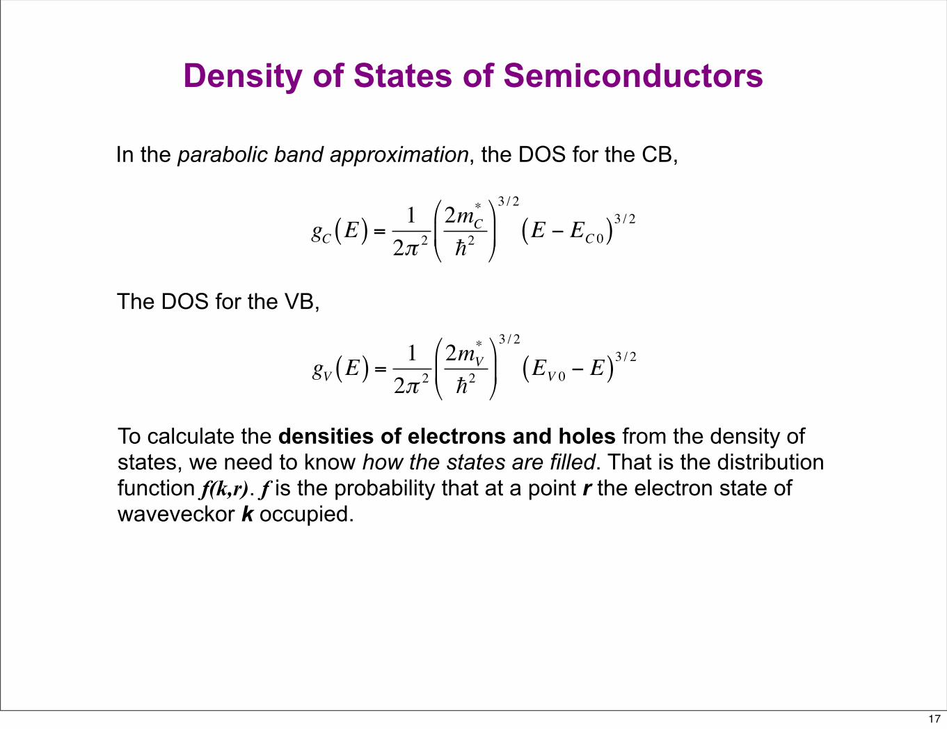
Density of States of Semiconductors
In the parabolic band approximation, the DOS for the CB,
€
gC E( ) =12π 2
2mC*
h2
3 / 2
E − EC 0( )3 / 2
€
gV E( ) =12π 2
2mV*
h2
3 / 2
EV 0 − E( )3 / 2
The DOS for the VB,
To calculate the densities of electrons and holes from the density of states, we need to know how the states are filled. That is the distribution function f(k,r). f is the probability that at a point r the electron state of waveveckor k occupied.
17

18

Semiconductor in Equilibrium
• Thermal Equilibrium• Fermi energy and Fermi Level• Fermi Dirac Distribution• Boltzmann Approximation• Electron/Hole Density in Equilibrium• Doping
19
Semiconductors in Equilibrium
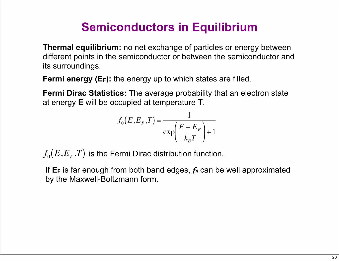
Fermi Dirac Statistics: The average probability that an electron state at energy E will be occupied at temperature T.
Fermi energy (EF): the energy up to which states are filled.
Thermal equilibrium: no net exchange of particles or energy between different points in the semiconductor or between the semiconductor and its surroundings.
€
f0 E,EF ,T( ) =1
exp E − EF
kBT
+1
is the Fermi Dirac distribution function.
€
f0 E,EF ,T( )If EF is far enough from both band edges, f0 can be well approximated by the Maxwell-Boltzmann form.
20

E
E
E
E
EF
EF
EF
EF
g(E)
f(E)
n(E)
n(E)
1
0
T=0
(T=0)
T>0
(T>0)
The total density of electrons in CB and holes in VB are
€
n = gC E( ) f0 E,EF ,T( )dEEC
∞
∫
€
p = gV E( ) 1− f0 E,EF ,T( )( )dE−∞
EV∫
Semiconductors in Equilibrium
21

In the conduction band, as E>>EF,
€
f0 E,EF ,T( ) ≈ exp EF − EkBT
In the valence band, as E<<EF,
€
1− f0 E,EF ,T( ) ≈ exp E − EF
kBT
Then the electron density
€
n = NC expEF − EC
kBT
NC is the effective conduction band density of states and
€
NC = 2 mC* kBT2πh2
3 / 2
Electron Densities in Equilibrium
22

€
p = NV expEV − EF
kBT
For the hole density
NV is the effective valence band density of states and
€
NV = 2 mV* kBT2πh2
3 / 2
For any given material at a given temperature the product np is a constant:
€
np = NCNV exp−Eg
kBT
Intrinsic carrier density (ni): It is equal to the density of electrons thermally excited into the CB of a pure semiconductor in thermal equilibrium.
€
ni2 = np = NCNV exp
−Eg
kBT
Hole Densities in Equilibrium
23

€
n = ni expEF − Ei
kBT
p = ni expEi − EF
kBT
It is sometimes convenient to write n and p in terms of ni and an intrinsic potential energy Ei,
€
Ei =12EC + EV( ) − 1
2kBT ln
NC
NV
=12EC + EV( ) − 3
4kBT ln
mC*
mV*
where
Ei is an energy close to the center of the band gap and is equal to the Fermi level of the pure semiconductor in equilibrium.
Electron and Hole Densities in Equilibrium
24

Electron affinity of the semiconductor (χ): the least amount of energy required to remove an electron from the solid. It is measured from the conduction band edge to the vacuum level EVAC.
Vacuum level (EVAC): the energy to which an electron must be raised to be free of all forces from the solid.
Electron and Hole Densities in Equilibrium
€
EC = EVAC − χ
EV = EVAC − χ − Eg
EF = EVAC − χ + kBT ln n /NC( )= EVAC − χ − Eg − kBT ln p /NV( )
EC
EV
EF
χ
Evac
-kBT ln(n/NC)
-kBT ln(p/NV)
25
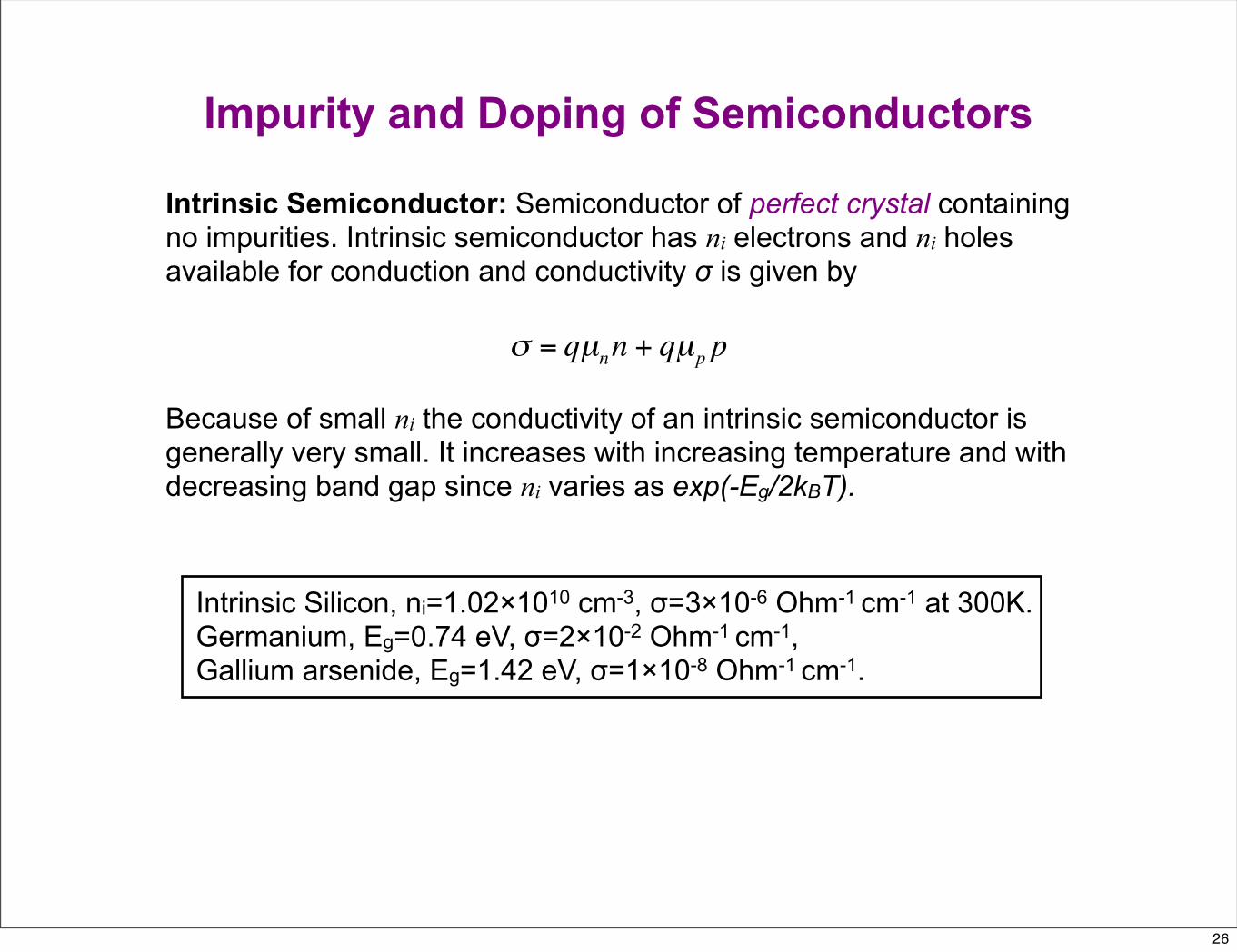
Impurity and Doping of Semiconductors
Intrinsic Semiconductor: Semiconductor of perfect crystal containing no impurities. Intrinsic semiconductor has ni electrons and ni holes available for conduction and conductivity σ is given by
€
σ = qµnn + qµp p
Because of small ni the conductivity of an intrinsic semiconductor is generally very small. It increases with increasing temperature and with decreasing band gap since ni varies as exp(-Eg/2kBT).
Intrinsic Silicon, ni=1.02×1010 cm-3, σ=3×10⁻⁶ Ohm-1 cm-1 at 300K.Germanium, Eg=0.74 eV, σ=2×10⁻² Ohm-1 cm-1,Gallium arsenide, Eg=1.42 eV, σ=1×10⁻⁸ Ohm-1 cm-1.
26

The impurity or defect introduces bonds of different strength to those which make up the perfect crystal, and therefore changes the local distribution of electronic energy levels.
The altered energy levels are localized, unlike the intrinsic conduction and valence band states. If the impurity energy level occur within the band gap they can affect the electronic properties of the semiconductor:Introducing occupied impurity energy levels above Ei increases the Fermi level, which increases the density of electrons relative to holes in equilibrium. Unoccupied level below Ei reduce the Fermi level and increase the density of holes relative to electrons.
Doping: The density and the nature of the carriers in the semiconductor can be controlled by adding definite amounts of impurities with energy levels close to the conduction or valence band edge.
Impurity and Doping of Semiconductors
27

Impurity and Doping of Semiconductors
n-type Semiconductor: With occupied energy levels between Ei and EC, a semiconductor has been doped by replacing some of the atoms in the crystal lattice with impurity donor atoms, to increase the density of electrons relative to holes. The principle charge carriers are negative. p-type Semiconductor: With unoccupied energy levels between EV and Ei, a semiconductor has been doped by replacing some of the atoms in the crystal lattice with impurity acceptor atoms, to increase the density of holes relative to electrons. The principle charge carriers are positive.
++
n-type doping p-type doping
28

In the band picture, the donor electrons have been promoted from a level in the band gap, Vn below EC, into the CB. The acceptor energy level appears in the band gap close to the VB edge.
The density of carriers can be controlled by varying the density of dopants. If Nd>>ni, and the donors are fully ionized at room temperature, then
€
n ≈ Nd
And since at equilibrium
€
p = ni2 /Nd
€
np = ni2
Impurity and Doping of Semiconductors
EC
EV
EFVn
donor level
EC
EV
EFVp
acceptor level
29

CB
VB
EF
Intrinsic
CB
VB
EF
donor level
n-type
CB
VBEF
acceptor level
p-type
In an intrinsic semiconductor, EF lies roughly in the middle of the band gap. The effect of doping is to shift the Fermi level away from the center of the band gap, towards EC in n-type material, and towards EV in p-type material.
Impurity and Doping of Semiconductors
30

Advantage: Unlike heating and illumination, doping is a way to increase the conductivity of the semiconductor at equilibrium without requiring a constant input of energy.Disadvantage: Heavy doping causes imperfections in the crystal structure which appear at states in the band gap close to the CB and VB edges, having the effect of adding a tail to the CB and VB density of states functions, and so effectively reducing the band gap. As a photovoltaic material, heavy doping is likely to increase the density of defect states which act as centers for carrier recombination or trapping.
Amorphous semiconductor: Have a similar structure to the crystal on the short range, but have no long range order. The small deviation of bond length and orientation give rise to a spread in energy level so that the DOS near the CB minimum and VB maximum tends to decay with energy into the band gap, rather than cutting off abruptly.
Impurity and Doping of Semiconductors
31

Semiconductor under Bias
• Semiconductor under Bias• Quasi Thermal Equilibrium• Quasi Fermi Level• Effective Temperature and Hot Electron
32

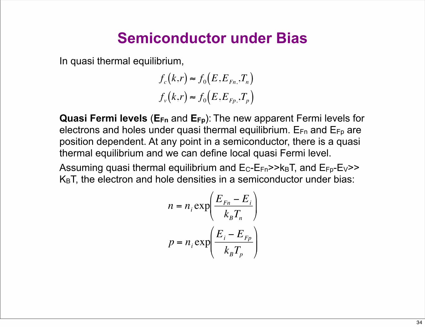
Semiconductor under Bias
To understand the operation of a solar cell, we need to understand what happens to the semiconductor when it is displaced from equilibrium by exposure to light or electrical injection of electrons and holes through an applied electric bias. In either case, n and p have been disturbed so that they are no longer described by the Fermi Dirac distribution.
Quasi thermal equilibrium: If the disturbance is not too great, or not changing too quickly, the populations of electrons and holes relax to achieve a state called quasi thermal equilibrium. The population of electrons within the CB distribute themselves as though they were at equilibrium, with a common Fermi level and temperature. The holes within the valence band arrange themselves as though they shared another different Fermi level and possibly a different temperature.
33
€
fc k,r( ) ≈ f0 E,EFn,,Tn( )fv k,r( ) ≈ f0 E,EFp,,Tp( )
Quasi Fermi levels (EFn and EFp): The new apparent Fermi levels for electrons and holes under quasi thermal equilibrium. EFn and EFp are position dependent. At any point in a semiconductor, there is a quasi thermal equilibrium and we can define local quasi Fermi level.
In quasi thermal equilibrium,
Semiconductor under Bias
Assuming quasi thermal equilibrium and EC-EFn>>kBT, and EFp-EV>> KBT, the electron and hole densities in a semiconductor under bias:
€
n = ni expEFn − Ei
kBTn
p = ni expEi − EFp
kBTp
34

Semiconductor under Bias
€
n = NC exp− EC − EFn( )
kBTn
p = NV exp− EFp − EV( )
kBTp
Or
Tn and Tp are the electron and hole effective temperatures, and may be different from ambient temperature.
Hot electron: Electrons with Tn>T are called hot electrons and can arise in situations where the carriers gain excess kinetic energy from strong electric fields.
fs
fs
µs
35

Electron and Hole Densities under Bias
CB
VB
EF
Equilibrium
n0 electrons
p0 holes
CB
VB
EFn >EF
Under bias
>>n0 electrons
>>p0 holesEFp<EF
Fermi level splits:
€
EFn ≠ EFp ≠ EF
€
Δµ = EFn − EFp
€
np = ni2 exp Δµ
kBT
36
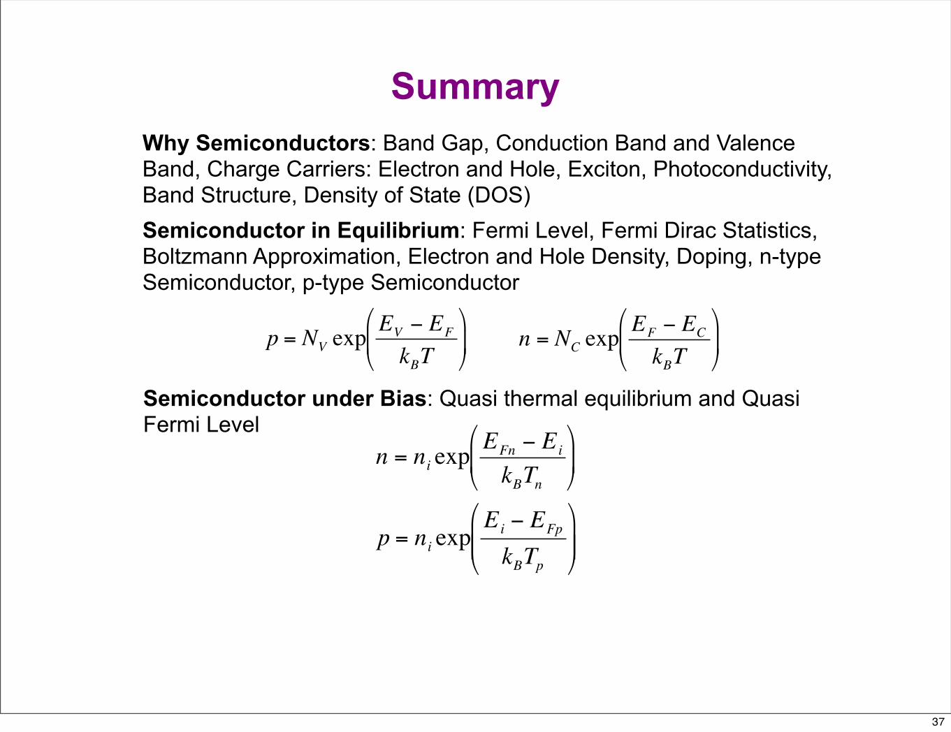
SummaryWhy Semiconductors: Band Gap, Conduction Band and Valence Band, Charge Carriers: Electron and Hole, Exciton, Photoconductivity, Band Structure, Density of State (DOS)Semiconductor in Equilibrium: Fermi Level, Fermi Dirac Statistics, Boltzmann Approximation, Electron and Hole Density, Doping, n-type Semiconductor, p-type Semiconductor
€
n = ni expEFn − Ei
kBTn
p = ni expEi − EFp
kBTp
€
n = NC expEF − EC
kBT
€
p = NV expEV − EF
kBT
Semiconductor under Bias: Quasi thermal equilibrium and Quasi Fermi Level
37