LASER MICROMACHINING OF SILICON: A NEW TECHNIQUE … · A NEW TECHNIQUE FOR FABRICATING HIGH...
19
Eighth international Symposium on Space Terahertz Technology, Harvard University, March 1997 LASER MICROMACHINING OF SILICON: A NEW TECHNIQUE FOR FABRICATING HIGH QUALITY TERAHERTZ WAVEGUIDE COMPONENTS' C. K. Walker, G. Narayanan, H. Knoepfle, J. Capara, J. Glenn, A. Hungerford. Steward Observatory, University of Arizona, Tucson, AZ 85721 and T. M. Bloomstein, S. T. Palmacci, M. B. Stern, and J. E. Curtin Lincoln Laboratory, Massachusetts Institute of Technology, Lexington, MA 02173 ABSTRACT One of the main obstacles encountered in designing low noise, high efficiency, heterodyne receivers and local oscillator sources at submillimeter wavelengths is the quality and cost of waveguide structures. At wavelengths shorter than 400 mi- crometers, rectangular waveguide structures, feedhorns, and backshorts become extremely difficult to fabricate using standard machining techniques. We have used a new laser milling technique to fabricate high quality, THz waveguide com- ponents and feedhorns. Once metallized, the structures have the properties of standard waveguide components. Unlike waveguide components made using sil- icon wet-etching techniques, laser-etched components can have almost any cross section, from rectangular to circular. Under computer control, the entire wave- guide structure (including the corrugated feedhorn!) of a submillimeter-wave mixer or multiplier can be fabricated to micrometer tolerances in a few hours. Laser etching permits the direct scaling of successful waveguide multiplier and mixer designs to THz frequencies. Since the entire process is computer con- trolled, the cost of fabricating submillimeter waveguide components is signific- antly reduced. With this new laser etching process, the construction of high ' The Lincoln Laboratory portion of this work was performed under a cooperative research and development agreement (CRDA) with the University of Arizona. Opinions, interpret- ations, conclusions, and recommendations are those of the author and are not necessarily endorsed by the United States Government. 358
Transcript of LASER MICROMACHINING OF SILICON: A NEW TECHNIQUE … · A NEW TECHNIQUE FOR FABRICATING HIGH...

Eighth international Symposium on Space Terahertz Technology, Harvard University, March 1997
LASER MICROMACHINING OF SILICON:A NEW TECHNIQUE FOR FABRICATING
HIGH QUALITY TERAHERTZ WAVEGUIDE COMPONENTS'
C. K. Walker, G. Narayanan, H. Knoepfle, J. Capara, J. Glenn, A. Hungerford.
Steward Observatory, University of Arizona, Tucson, AZ 85721
and
T. M. Bloomstein, S. T. Palmacci, M. B. Stern, and J. E. Curtin
Lincoln Laboratory, Massachusetts Institute of Technology, Lexington, MA 02173
ABSTRACT
One of the main obstacles encountered in designing low noise, high efficiency,
heterodyne receivers and local oscillator sources at submillimeter wavelengths is
the quality and cost of waveguide structures. At wavelengths shorter than 400 mi-
crometers, rectangular waveguide structures, feedhorns, and backshorts become
extremely difficult to fabricate using standard machining techniques. We have
used a new laser milling technique to fabricate high quality, THz waveguide com-
ponents and feedhorns. Once metallized, the structures have the properties of
standard waveguide components. Unlike waveguide components made using sil-
icon wet-etching techniques, laser-etched components can have almost any cross
section, from rectangular to circular. Under computer control, the entire wave-
guide structure (including the corrugated feedhorn!) of a submillimeter-wave
mixer or multiplier can be fabricated to micrometer tolerances in a few hours.
Laser etching permits the direct scaling of successful waveguide multiplier and
mixer designs to THz frequencies. Since the entire process is computer con-
trolled, the cost of fabricating submillimeter waveguide components is signific-
antly reduced. With this new laser etching process, the construction of high
'The Lincoln Laboratory portion of this work was performed under a cooperative research
and development agreement (CRDA) with the University of Arizona. Opinions, interpret-
ations, conclusions, and recommendations are those of the author and are not necessarily
endorsed by the United States Government.
358

Eighth International Symposium on Space Terahertz Technology, Harvard University, March 1997
performance waveguide array receivers at THz frequencies becomes tractable. In
this paper we describe the laser etching technique and discuss test results from a
micromachined 2 THz feedhorn.
1 Motivation
The vast majority of radio receivers, transmitters, and components that operate at milli-
meter and submillimeter wavelengths utilize waveguide structures in some form. This is
because waveguide is a well characterized, low-loss, transmission medium which can be read-
ily fashioned into a variety of high-quality circuit and quasi-optical components. The long
history of development of waveguide components provides a broad base of knowledge from
which to synthesize and evaluate new designs. In addition, new computer aided design tools
(e.g. Hewlett Packard's High Frequency Structure Simulator) provide a straightforward way
of optimizing even complicated waveguide structures. Unfortunately, at frequencies above
1 THz, waveguide dimensions become so small (less than 0.23 by 0.116 mm) that fabrication
utilizing conventional machining and electroforming techniques becomes extremely difficult,
expensive, and/or impossible. Indeed, for situations where even modest sized heterodyne
array receivers are being considered, the practical frequency limit to utilizing conventional
machined waveguide structures is much lower 500 GHz). This situation is unfortunate,
since, due to their lower loss and tuning flexibility, waveguide mixers have been found to (in
general) outperform quasi-optical mixers both electrically and optically at frequencies where
both have been constructed. Clearly, a new way of machining small waveguide structures is
needed in order to reap the benefits of waveguide at THz freqencies.
In the past, silicon wet etching techniques have been employed as an alternative to
conventional machining [1, 2]. The main disadvantage of the wet etching technique is that
one is forced to follow the < 100 > or < 110 > crystal plane in the silicon. This severely
limits the types of structures that can be produced. The process is well suited to making
wide-angle pyramidal horns or straight sections of single height waveguide. However, it
cannot readily be used to make waveguide structures in which the height of the waveguide is
stepped down (e.g. in an impedance transformer) or tapered (either rectangular or circular).
These structures are needed to make efficient feedhorns.
359

Eighth International Symposium on Space Terahertz Technology, Harvard University, March 1997
In this paper we introduce a new laser micromachining technique for fabricating high
quality, low-cost waveguide structures for frequencies up to 10 THz. With this process,
waveguide components of varying height and width can be machined to 1 pm accuracy.
As a test of the viability of the laser micromachining technology, we conducted beam pattern
measurements on a 2 THz corrugated feedhorn made using this process.
Waveguide Fabrication
2.1 Laser Induced Microchemical Etching of Silicon
Laser processing offers several advantages for machining parts in the micro-domain. Com-
pared to conventional machining, smaller feature sizes with greater mechanical tolerances can
typically be achieved due to the high focusability of laser light and ability to deliver intense
sources of energy with high precision. Since laser machining is a non-contact process, there
is no mechanically-induced material damage, tool-wear, or machine vibration from cutting
forces. This can lead to finer finishes, improved accuracy, and less process overhead. A
number of different materials ranging from metals and polymers to composites and ceramics
have been successfully machined using lasers, traditionally using ablative techniques.
For the waveguide application, we employ a laser-induced microreaction initially de-
veloped for trimming and trench etching of silicon in semiconductor microfabrication [3,4,5].
As explained below, there are several important advantages to using chemical action for the
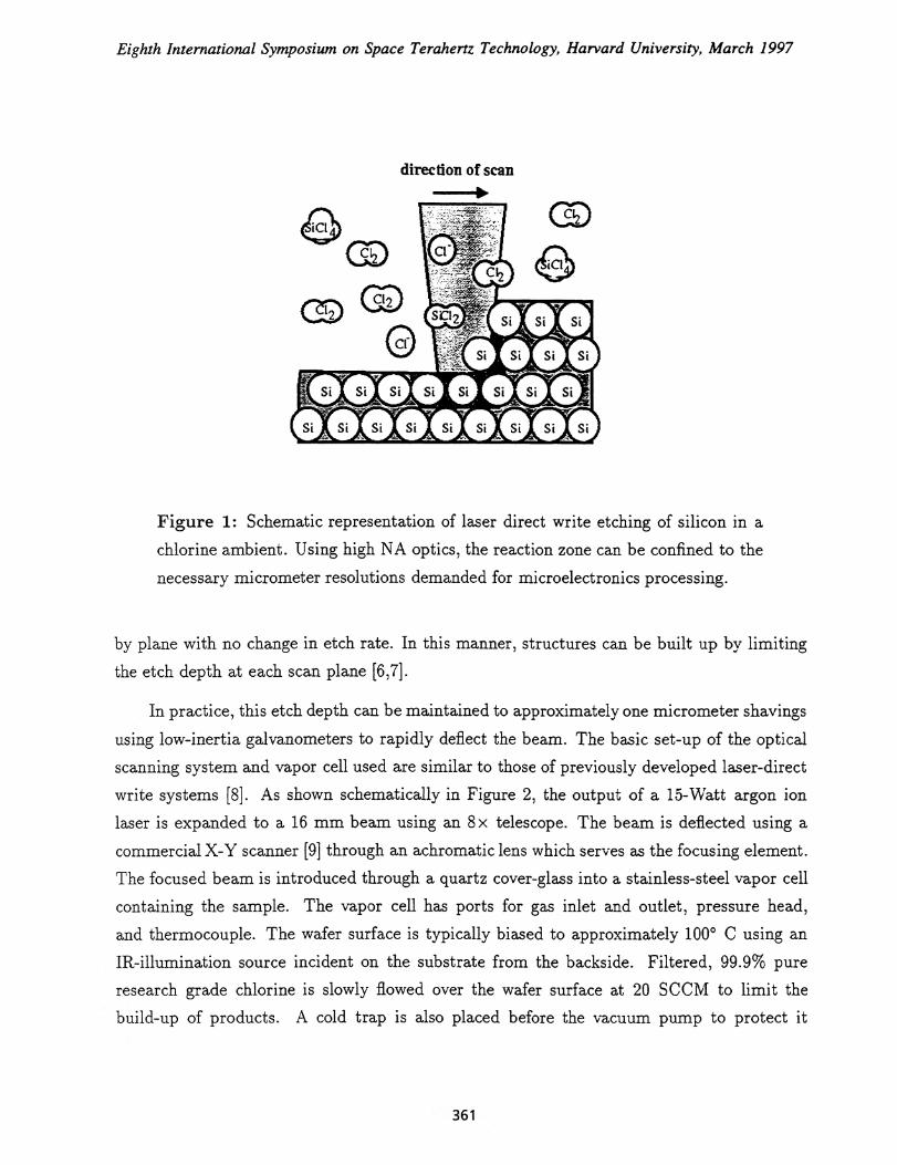
controlled removal of material. The basic process is shown schematically in Figure 1. An
argon-ion laser is used to locally heat a portion of the silicon substrate in a chlorine ambient.
At the onset of melting, volatile silicon chlorides are formed. Due to the highly non-linear ac-
tivation energy of the process, the reaction is confined almost exclusively to the molten zone.
Also, silicon is bound into volatile products unlike ablative techniques which due to their
explosive nature, can lead to particulate formation. These are often very difficult to remove
due to significant attractive forces in the micro-domain. Chemical activation also reduces the
energy requirement for removal minimizing the potential for cracking. Using a crystalline
material such as silicon also has the benefit that unetched portions of the molten zone regrow
epitaxially to crystalline quality. This allows controlled thin shavings to be removed plane
360
Eighth International Symposium on Space Terahertz Technology, Harvard University, March 1997
direction of scan
Figure 1: Schematic representation of laser direct write etching of silicon in a
chlorine ambient. Using high NA optics, the reaction zone can be confined to the
necessary micrometer resolutions demanded for microelectronics processing.
by plane with no change in etch rate. In this manner, structures can be built up by limiting
the etch depth at each scan plane {6,7].
In practice, this etch depth can be maintained to approximately one micrometer shavings
using low-inertia galvanometers to rapidly deflect the beam. The basic set-up of the optical
scanning system and vapor cell used are similar to those of previously developed laser-direct
write systems [8]. As shown schematically in Figure 2, the output of a 15-Watt argon ion
laser is expanded to a 16 mm beam using an 8 x telescope. The beam is deflected using a
commercial X-Y scanner [9} through an achromatic lens which serves as the focusing element.
The focused beam is introduced through a quartz cover-glass into a stainless-steel vapor cell
containing the sample. The vapor cell has ports for gas inlet and outlet, pressure head,
and thermocouple. The wafer surface is typically biased to approximately 100° C using an
IR-illumination source incident on the substrate from the backside. Filtered, 99.9% pure
research grade chlorine is slowly flowed over the wafer surface at 20 SCCM to limit the
build-up of products. A cold trap is also placed before the vacuum pump to protect it
361

1%) CUSSINPTIC UARTZ WINDOW
U BSTRATEPUMP
1R-SOU RCE
ECHANICALSH UTTE R
ri PHOTO-DIODE
GA LVO
15-WATT ex BEAMARGON-IO N EXPANDER088-514 nil)
4.0
GALVO
Z-AXIS
0 UA RTZ STU
STAGE
Eighth International Symposium on Space Terahertz Technology, Harvard University, March 1997
Figure 2: Schematic diagram of galvanometer based scanning apparatus. A
higher power objective (not shown) can be slid in place of the focusing optic to
allow more detailed analysis of the surface. For etching high aspect ratio struc-
tures, a circular polarizer is placed in the beam path to improve edge uniformity
due to the selective reflectivity of the S and P polarization components along the
side-walls.
from the corrosive gas. The reaction is observed through the focusing optic with a charge
coupled device (CCD) camera. A high power 50x objective is also mounted on a linear
translation stage containing the focusing element allowing details on the surface to be more
closely examined in-situ. The scanning system is driven directly from computer generated
patterns which can be constructed using a commercial solid-modeling software package or
via software using a toolbox of simple shapes.
A detailed description of the process physics can be found in [10]. Below, we summarize
the results. The volumetric removal rate (Vol Rate) is found experimentally to scale according
362

Eighth International Symposium on Space Terahertz Technology, Harvard University, March 1997
to:
Vol Rate = 104pm2/s(TA/300K)°-8wm
where TA is the temperature of the ambient gas and Wm is the diameter of the molten zone.
The proportionality constant is determined by the complicated transport and reaction dy-
namics, particularly from gas phase chemical reactions which alter the dynamics through
compositional changes and heats of reaction. The temperature scaling is due to the improved
diffusive transport of species to and from the chemically active area in the gas-phase localized
above the molten zone. The gas ambient temperature (equal to the bias temperature of the
substrate) can be continually increased to approximately 700 K. At higher temperatures, sig-
nificant background etching of the substrate occurs. Additional laser energy can also initiate
a self-sustained reaction leading to highly damaged and coarse looking surfaces. The removal
rate is also found to scale directly with the radius of the molten zone. This linear scaling of
removal rate with reaction zone is characteristic of systems with three dimensional transport
such as in the combustion of fuel droplets. The melt zone diameter is dependent on the laser
power, optical coupling, and thermal properties of silicon. In practice, the melt zone can be
varied from 1 to 25 pm using a 15 Watt argon-ion laser running multi-mode. This leads
to removal rates ranging from approximately 104 1um3/s (1036 mm3/hr) to 5 x 10⁵ pm3/s
(1.8 mm3ihr). By virtue of the scaling law, smaller, higher frequency waveguide compon-
ents can be fabricated in even less time since volumetric removal rates scale linearly with
melt zone diameter, or resolution, while the total volume of the device scales cubically with
length scale. For instance, a similar 1.62 THz waveguide at 4-pm resolution can be etched
in one-fourth the time of an 810 GHz version etched at 8-ym resolution.
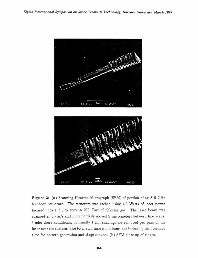
As an example of a laser micromachined part, a proof-of-concept demonstration was
made of a portion of an 810 GHz and 2 THz circular to rectangular mode matching wave-
guide. In the initial prototyping of the 810 GHz waveguide structure, an approximately 8
pm diameter laser-induced reaction zone (6-pm laser beam spot size) is swept across the
surface at 5 cm/s removing 1 ym shavings per plane at a rate of 10 5pm3 /s. Higher scanning
velocities can be used to increase depth resolution. Improved lateral resolutions, if necessary,
are possible over critical dimensions through power modulation of the laser beam. Figure
3 shows a portion of the waveguide structure etched in 1 hour (a duplicate mating piece
must be fabricated). A larger portion of the feedhorn is shown in Figure 4. For the 2 THz
363
Eighth International Symposium on Space Terahertz Technology, Harvard University, March 1997
Figure 3: (a) Scanning Electron Micrograph (SEM) of portion of an 810 GHz
feedhorn structure. The structure was etched using 4.3 Watts of laser power
focused into a 6 pm spot in 200 Torr of chlorine gas. The laser beam was
scanned at :5 cm/s and incrementally moved 2 micrometers between line scans.
Under these conditions, nominally 1 pm shavings are removed per pass of the
laser o‘-er the surface. The total etch time is one hour, not including the overhead
time for pattern generation and stage motion. (b) SEM close-up of ridges.
364

Eighth International Symposium on Space Terahertz Technology, Harvard University, March 1997
Figure 4: SENI of the first twenty-ridges in the feedhorn portion of the 810 GHz
structure. The same processing conditions described in Figure 3 were used. This
extended portion of the feedhorn required two hours to fabricate, not including
the overhead time for pattern generation and stage motion.
device, an approximately 4 ttm (3-ym laser beam spot size) diameter laser-induced reaction
zone is swept across the surface at 4 cm/s removing 0.65 pm shavings per plane at a rate of
5 x 10' m3/s. Figure 5 show scanning electron micrographs of the structures.
Waveguide surface roughness values measured with atomic force microscopy are typically
on the order of 200 nm RMS. This surface quality is already sufficient to provide low-
loss waveguide performance to > 10 THz. The RMS surface roughness can be reduced
even further, to under 25 nm, using standard polishing etches based on HF-HNO3-HC211302
solutions.
365

Eighth International Symposium on Space Terahertz Technology, Harvard University, March 1997
Figure 5: (a) SEM micrograph of replicated version of 2 THz waveguide struc-
ture. The original structure was etched using 3 Watts of laser power focused into
a 4 ym spot in 200 Torr of chlorine gas. The laser beam was scanned at 4 cm/s
and incrementally moved 2 micrometers between line scans removing 0.65 ym
shavings per pass of the laser over the surface. (b) SEM close-up of ridges.
366

Eighth International Symposium on Space Terahertz Technology, Harvard University, March 1997
2.2 Device Replication
Although the process can be used to produce prototypes relatively quickly, to produce large
format arrays, it becomes more practical to replicate the etched devices. We are currently
working on a polymer based replication process [11] to produce high performance, low-cost,
focal plane arrays at THz frequencies. This molding process has shown extremely high
fidelity in reproducing features down to sub-micrometer detail. A negative of the silicon
etched master is first made by casting polydimethylsiloxane (PDMS) over the etched surface
which has been first fluorinated with tridecafluoroctaltrichlorosilane (TDTS). Due to the
high elastomeric constant and low interfacial free energy between PDMS and the surface,
it can be readily pulled apart from the silicon master. A low-viscosity polymer precursor,
such as uv-curable epoxy, polyurethane, or polymethylmethacrylate is then flowed over the
elastomer negative, filling the structure through capillary action. After curing, the elastomer
is pulled from the epoxy replica for further reuse. A portion of a replicated version in five
minute uv-cured epoxy of a 2.0 THz waveguide structure is shown in Figure 6 showing the
excellent fidelity of the process. After the structures are replicated in epoxy, 0.3 Am of gold
are sputtered onto the waveguide surface. The structures are then mated using uv-cureable
epoxy in a double sided aligner we have implemented. Cross-hairs etched off to the side of the
waveguide on the silicon master and masked during the gold sputtering are used as guides in
the mating procedure. A summary of the replication and coating process is shown in Table
Beam Pattern of a 2 THz Laser Micromachined Feed-horn
Using the process described above, two 2 THz corrugated feedhorns were fabricated in an
end-to-end arrangement as shown in Figure 5a. The feedhorn design follows that of [12]
and has 30 corrugations. The two horns are connected by a short (0.164 mm ) section of
circular waveguide. Once the two halves of the horn blocks have been aligned and mated,
they are clamped into a test fixture (Figure 7). The beam of one feedhorn looks through a
far-infrared, low-pass filter (0.8 mm thick crystalline quartz with garnet powder and a black
367

Eighth International Symposium on Space Terahertz Technology, Harvard University, March 1997
Figure 6: SE.M micrograph of replicated version of 2 THz waveguide.
polyethylene layer) and polyethelene vacuum window into an anechoic chamber. It is this
feedhorn on which the beam pattern measurement is performed. An additional 25/..tm)
layer of black polyethylene was placed across the vacuum window to further reduce the
possibility of near/mid infrared light leaks. The second feedhorn looks down into a reflective
cavity containing a doped silicon bolometer [13] designed to operate at 4 K. Together the
low-pass filter and feedhorns limit the frequency response of the bolometer to between 1.4
and 2.4 THz. The voltage output of the bolometer is proportional to the power intercepted
by the input feedhorn over this frequency range. The downward looking cryostat containing
the detector assembly is mounted on top of an air tight anechoic chamber as shown in Figure
8. The humidity in the chamber can be lowered by filling it with dry nitrogen gas and/or
with a tray of dessicant. The chamber contains a large (42" travel), computer-controlled,
X-Y stage. A calibrated, upward looking, black-body source is mounted on the stage and
serves as the signal source for beam pattern measurements. For the measurements described
here the temperature of the blackbody source was set to 950 K. The blackbody aperture is
368

4. PEEL OFF ELASTOMER ANDACETATE AND SPUTTERGOLD ON EPDXY REPLICA
1. LASER ETCH WAVEGUIDE
2. PRIME SUBSTRATE WITHRELEASE AGENT ANDCREATE ELASTOMERMASTER FROM PDMS(NEGATIVE TONE)
3. REPLICATE ELASTOMER INUV-CURED EPDXY ONACETATE SUBSTRATE
SputteredGold
/.;
7111■••■•••■•••••■
Epoxy /\
Eighth International Symposium on Space Terahertz Technology, Harvard University, March 1997
Table 1: Replication and Gold Sputtering Process
chopped at 20 Hz. Beam pattern measurements are made by scanning the blackbody under the
test de-war and synchronously detecting the bolometer output using a lock-in amplifier. The
control computer records the position of the black body source along with the corresponding
lock-in amplifier output. The distance between the black body source and feedhorn (234 mm)
provides an angular resolution of 1.47°.
Figure 9 shows cross-scans of the 2 THz feedhorn. The plots indicate the feedhorn's beam
is nearly Gaussian with no measurable sidelobes to the noise floor of the map 11 dB).
There is a small asymmetry in the beam patterns, probably the result of a slight misalignment
between the two halves of the horn block. The FWHM of the beam profile is ,-- 20°, close to
the value of 19.3° derived from the horn's beamwaist, coo = 0.33 d, where d is the diameter
of the feedhorn aperture 0.506 mm.
369

TEST HORN FILTERBOLOMETER BOLINETER DI AS
VACUUM WINDOW
4K COLD PLATETO AWL! FIER
Eighth International Symposium on Space Terahertz Technology, Harvard University, March 1997
BEAM TEST CRYOSTAT
Figure 7: Cross section of feedhorn test fixture mounted in the cryostat. The
beam of one feedhorn looks through a far-infrared, low-pass filter (0.8 mm thick
crystalline quartz with garnet powder with a black polyethylene layer) and poly-
ethelene vacuum window into an anechoic chamber. The second feedhorn looks
down into a reflective cavity containing a doped silicon bolometer [13] designed
to operate at 4 K.
4 Applications
4.1 Mixer Arrays
With this new micromachining technology it is now possible to consider the construction of
large format arrays of high-performance THz waveguide receivers. Figures 10, 11a, 11b, and
lic illustrate how a 2 THz array of hot-electron bolometer mixers could be constructed using
this technology.
Figure 10 is an assembly diagram of the mixer array. The design uses an array of
corrugated feedhorns, each with a reduced-height waveguide transition (Fig. 11a). The
370

Eighth International Symposium on Space Terahertz Technology, Harvard University, March 1997
THz BEAM PATTERN RANGE
Figure 8: THz Beam Pattern Range. The chamber contains a large (42" x 42"
travel), computer-controlled, X-Y stage. A calibrated, upward looking, black-
body source is mounted on the stage and serves as the signal source for beam
pattern measurements.
reduced-height waveguide should provide an excellent match to the real part of the bolometer
impedance, permitting the use of only a single, fixed backshort.
At high frequencies (> 650 GHz) it becomes nearly impossible to manually mount
detectors across small waveguide structures. In order to avoid this problem, mixing devices
for the array are fabricated on pm thick silicon nitride membranes. To date, this approach
has been successful with SIS junctions up to frequencies of --850 GHz. Here, the bolometers
are fabricated on membranes which span an aperture with the dimensions of the reduced
height waveg-uide used in the 'horn block'. These apertures are formed by etching a pyramidal
hole from the backside of the silicon wafer supporting the membrane (see Fig. 11b). As with
the horn block, all exposed surfaces of silicon are gold plated to provide conduction. The
bolometers are placed in the center of the waveguide. Low pass filtering is provided by a
371

-30 -20 -10 0 10Angle (deg)
20 30
0.8
0.6
0.4
0.2
Eighth International Symposium on Space Terahertz Technology, Harvard University, March 1997
2 THz Beam Pattern
Figure 9: Beam cross scans of the micromachined 2 THz feedhorn. The 0 and
cks cuts are othogonal to each other.
microstrip circuit (see Fig 11c). Each IF output of the array is wire bonded to a microstrip
matching network located just outside the periphery of the Bolometer Array Block. Bolometer
bias is provided through the matching network.
The fixed backshort is a pyramidal structure designed to fit the cavity behind the mem-
brane. The backshorts can be readily made by wet-etching silicon through an SiO mask
evaporated on the wafer [2]. Once etched, the backshort wafer is gold plated.
4.2 Other Applications
With laser micromachining it now becomes possible to incorporate reactive posts and irises
in submillimeter waveguide designs. These structures would be particular useful in providing
a low-loss alternative to the end-loaded and radial stubs often used to tune out the capa-
citance of SIS junctions in waveguide mixer mounts. Below the gap frequency of niobium
690 GHz), where such stubs are less lossy, the addition of a properly chosen post or
iris can increase the instantaneous bandwidth of the mixer significantly over what would be
achieved with the tuning stub alone.
372

Fee
dh
orn
Blo
ck
Bolo
met
er A
rray
Blo
ck
Bac
ksh
ort
Blo
ck
Cor
ruga
ted
feed
horn
wit
hw
aveg
uid
e tr
ansi
tio
n t
ore
du
ced
hei
gh
t re
ctan
gula
rw
aveg
uide
Wir
e bo
ndin
g pa
ds4
Nio
bium
mic
robr
idge
bol
omet
eron I
urn
thic
k s
ilic
on
nit
rid
eCe
)m
embr
ane*
"tt 1Z) P*41
co tz)
Pyr
amid
al B
acks
hort
s
IF o
utp
ut
tran
smis
sio
n l
ine
Fig
ure
10
: S
ilic
on
mic
rom
ach
ined
arr
ay m
ixer
ass
embly
dia
gra
m.
The
arra
y m
ixer
co
nsi
sts
of
thre
eblo
cks:
a f
eedhorn
blo
ck,
a bo
lom
eter
arr
ay b
lock
on
wh
ich
HE
Bs
are
fab
rica
ted
acr
oss
sil
ico
n n
itri
de
win
do
ws,
and a
bac
ksh
ort
blo
ck.
Th
e h
orn
blo
ck i
s la
ser
mic
rom
ach
ined
. T
he
bo
lom
eter
arr
ay b
lock
an
dth
e bac
ksh
ort
blo
ck a
re m
icro
mac
hin
ed o
ut
of
sili
con
usi
ng
wet
etc
hin
g t
echn
iqu
es.

Horn Bloc
Backshort Wafer
Silicon NitrideMembrane
Bolometer
Low Pass Filter
Gold Metallization On TopOf Nitride Membrane
Ground Contact
Eighth International Symposium on Space Terahertz Technology, Harvard University, March 1997
(a) Cross—section View of Mixer Assembly
Bolometer Wafer
(b) Junction Wafer Block
Silicon Nit 'de Layer (1 urn)
Au Wiring Laye1 5.75
UM
25
Side View(c) Front View of Junction Wafer
To IF Connector
114 urn
Front View
Figure 11: Detailed drawings of a typical mixer in the array.
35:3
374
Eighth International Symposium on Space Terahertz Technology, Harvard University, March 1997
The design and construction of solid state frequency multipliers is often more difficult
to achieve than a single mixer [14]. The ability to micromachine reduced height waveg,uide
with the option of including irises and posts, will allow the designer greater flexibility in the
construction of high efficiency THz LO sources than have been available in the past.
Laser micromachining can also be used to make high performance submillimeter-wave
phase gratings [15, 16]. These gratings can serve as quasi-optical LO power splitters for
submillimeter array receivers.
The laser micromachining and replication process permits the construction of large num-
bers of high-efficiency feedhorns. Such horns could provide an alternative to Winston cones
in large format bolometer arrays where single mode optics are desired.
Summary
1. We have introduced a new technology for the fabrication of waveguide devices which
are difficult or impossible to manufacture using conventional techniques. We envision
structures operating at 1 through 10 THz (feature sizes of 300-30 micrometers) can be
fabricated with this technology.
2. With this technology it is now possible to construct large-format, waveguide imaging
arrays at THz frequencies.
3. This technology can also be used in the construction of efficient LO sources and quasi-
optical components at THz frequencies.
6 References
1 R. McGrath, C. K. Walker, M. Yap, and Y. Tai, IEEE Microwave and Guided Wave
Letters, vol 3, 61, 1993.
2 G. Rebeiz, G. W. Regehr, G. Wade, D. B. Rutledge, R. L. Savage, L. Richard, N. C.
Luhmann JR, Int. J. of IR ans MM Waves, vol 8, 1249, 1987.
375

Eighth International Symposium on Space Terahertz Technology, Harvard University, March 1997
3 D.J. Ehrlich, R.M. Osgood, Jr., and T.F. Deutsch, Appl. Phys. Lett., 38, 1018, 1981.
G.V. Treyz, R. Beach, and R.M. Osgood, Jr., J. Vac. Sci. Technol. B. 6, 37, 1988.
G.V. Treyz, R. Beach, and R.M. Osgood, Jr., Appl. Phys. Letters 50, 475, 1987.
T.M. Bloomstein and D.J. Ehrlich, in Technical Digest of Transducers (IEEE, New
York, 1992), pp. 507-511, 1991.
T.M. Bloomstein and D.J. Ehrlich, Appl. Phys. Lett. 61, 708, 1992.
8 Y.S. Liu, "Sources, optics, and laser microfabrication systems for direct writing and
projection lithography" in Laser Microfabrication, edited by D.J. Ehrlich and J.Y. Tsao
( Academic Press, San Diego, ch. 1., 1989.
9 See M3 Scanner/Driver User's Manual, Rev. A (General Scanning, Inc. Watertown,
MA, 1992).
10 T.M. Bloomstein, Sc.D. Thesis, Massachusetts Institute of Technology, 1996.
11 E. Kim, Y. Xia, and G.M. Whitesides, Nature 376, 581, 1985.
12 B. M. Thomas, IEEE Trans. Antennas and Propagation, 26, 267, 1978
13 Infrared Laboratories Inc., 1808 E 17th St., Tucson, Az.
14 N. Erickson, 1997, this volume.
15 G. F. Delgado and Bengtsson, 1194, Microwave and Optical Technology Letters, vol.
7, No. 18, pp. 831-834.
16 T. Klein, G. A. Ediss, R. Giisten, C. Kasemann, 1997, this volume.
376