On Particle Filters for Landmine Detection Using Impulse Ground ...

Landmine Detection Architectures And Their Implementation on FPGA
A thesis submitted in partial fulfillment of the requirements for the degree ofMaster of Science at George Mason University
By
Nikita CharankarBachelor of Engineering
University of Mumbai, 2006
Director: Dr. Kenneth J. Hintz, ProfessorDepartment of Electrical and Computer Engineering
Spring Semester 2010George Mason University
Fairfax, VA

ii
Copyright c© 2010 by Nikita CharankarAll Rights Reserved

iii
Dedication
I dedicate this thesis to my parents, Mr. and Mrs. Charankar.

iv
Acknowledgments
I would like to thank Dr. Kenneth J. Hintz, Dr. David Hwang and Dr. Nathalia Peixotofor believing in me and giving me this opportunity to work on this interesting thesis topicand especially, Dr. K. J. Hintz for his invaluable support, patience guidance throughoutthe thesis. I am thankful to Office of Naval Research (ONR) for funding this project. Ithank my team members, Dr. Ahmed Nasif for giving me the motivation and feedback onthe thesis and Preethi Rama Dev for being supportive and co-operative. I, also, thank Dr.Jens-Peter Kaps and all CERG members for their valuable time and support. I thank myadvisor, Dr. Jill Nelson for being available anytime in need and the entire faculty and staffof George Mason University for their co-operation. I would also like to thank my roommatesand all my dear friends for their moral support.
Last but not the least, I would like to thank my parents, my sister, Amita and my friend,Shreyas for being my pillars of strength, encouragement and motivation. Without them,this thesis would not have been possible.
v
Table of Contents
Page
List of Tables . . . . . . . . . . . . . . . . . . . . . . . . . . . . . . . . . . . . . . . . viii
List of Figures . . . . . . . . . . . . . . . . . . . . . . . . . . . . . . . . . . . . . . . . ix
Abstract . . . . . . . . . . . . . . . . . . . . . . . . . . . . . . . . . . . . . . . . . . . xi
1 Introduction . . . . . . . . . . . . . . . . . . . . . . . . . . . . . . . . . . . . . . 1
1.1 Motivation . . . . . . . . . . . . . . . . . . . . . . . . . . . . . . . . . . . . 1
1.2 Detection Techniques . . . . . . . . . . . . . . . . . . . . . . . . . . . . . . . 3
1.3 Previous Research . . . . . . . . . . . . . . . . . . . . . . . . . . . . . . . . 5
1.4 Hardware Implementation . . . . . . . . . . . . . . . . . . . . . . . . . . . . 6
1.5 Thesis Organization . . . . . . . . . . . . . . . . . . . . . . . . . . . . . . . 7
2 Ground Penetrating Radar . . . . . . . . . . . . . . . . . . . . . . . . . . . . . . 8
2.1 NIITEK GPR . . . . . . . . . . . . . . . . . . . . . . . . . . . . . . . . . . . 8
2.2 Syntactic Pattern Recognition Theory . . . . . . . . . . . . . . . . . . . . . 9
3 Hardware Implementation on FPGA . . . . . . . . . . . . . . . . . . . . . . . . . 12
3.1 Target Device . . . . . . . . . . . . . . . . . . . . . . . . . . . . . . . . . . . 12

vi
3.2 FPGA Hardware Programming . . . . . . . . . . . . . . . . . . . . . . . . . 13
3.3 FPGA Design Tools . . . . . . . . . . . . . . . . . . . . . . . . . . . . . . . 15
4 Previous Research . . . . . . . . . . . . . . . . . . . . . . . . . . . . . . . . . . . 17
4.1 Preprocessing Algorithm . . . . . . . . . . . . . . . . . . . . . . . . . . . . . 17
4.2 Landmine Discrimination . . . . . . . . . . . . . . . . . . . . . . . . . . . . 19
4.2.1 Reset Finite State Machine . . . . . . . . . . . . . . . . . . . . . . . 19
4.2.2 Parallel Correlator . . . . . . . . . . . . . . . . . . . . . . . . . . . . 20
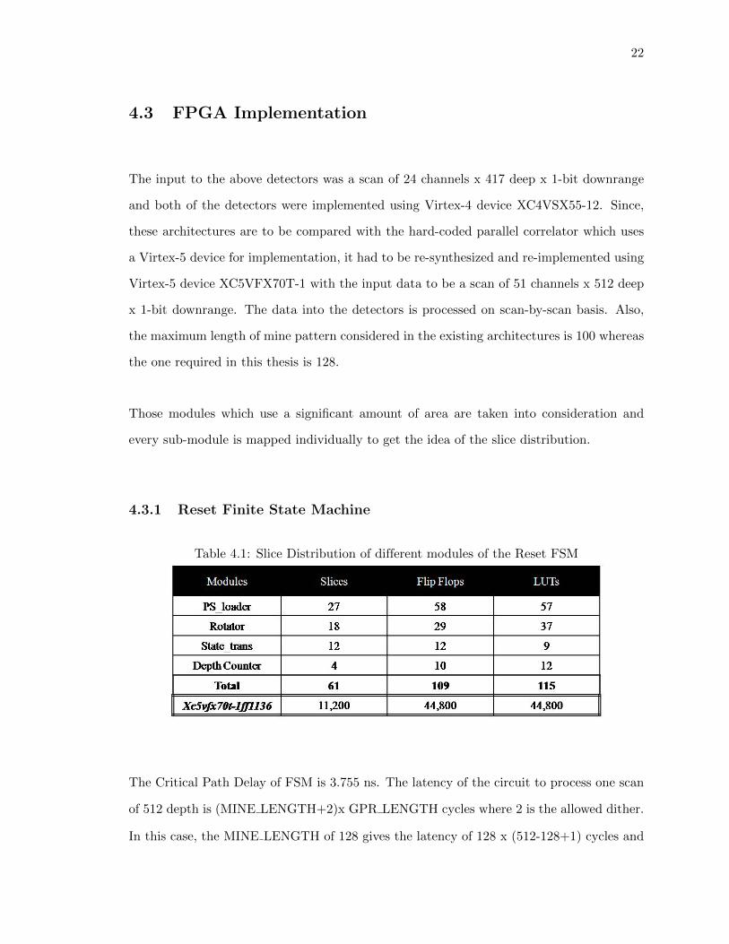
4.3 FPGA Implementation . . . . . . . . . . . . . . . . . . . . . . . . . . . . . . 22
4.3.1 Reset Finite State Machine . . . . . . . . . . . . . . . . . . . . . . . 22
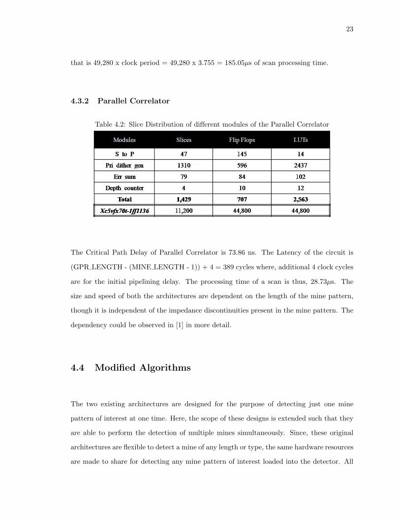
4.3.2 Parallel Correlator . . . . . . . . . . . . . . . . . . . . . . . . . . . . 23
4.4 Modified Algorithms . . . . . . . . . . . . . . . . . . . . . . . . . . . . . . . 23
4.4.1 FPGA Implementation . . . . . . . . . . . . . . . . . . . . . . . . . . 24
5 Hard-Coded Parallel Correlator . . . . . . . . . . . . . . . . . . . . . . . . . . . . 27
5.1 Architecture . . . . . . . . . . . . . . . . . . . . . . . . . . . . . . . . . . . . 28
5.2 FPGA Implementation . . . . . . . . . . . . . . . . . . . . . . . . . . . . . 30
6 RAM Based Finte State Machine . . . . . . . . . . . . . . . . . . . . . . . . . . . 36
6.1 Architecture . . . . . . . . . . . . . . . . . . . . . . . . . . . . . . . . . . . . 38
6.2 FPGA Implementation . . . . . . . . . . . . . . . . . . . . . . . . . . . . . . 39
7 Conclustion and Scope . . . . . . . . . . . . . . . . . . . . . . . . . . . . . . . . . 44

vii
7.1 Conclusion . . . . . . . . . . . . . . . . . . . . . . . . . . . . . . . . . . . . 44
7.2 Scope and Suggestions . . . . . . . . . . . . . . . . . . . . . . . . . . . . . . 47
A Appendix . . . . . . . . . . . . . . . . . . . . . . . . . . . . . . . . . . . . . . . . 48
Bibliography . . . . . . . . . . . . . . . . . . . . . . . . . . . . . . . . . . . . . . . . . 49
viii
List of Tables
Table Page
4.1 Slice Distribution of Reset FSM . . . . . . . . . . . . . . . . . . . . . . . . . 22
4.2 Slice Distribution of Parallel Correlator . . . . . . . . . . . . . . . . . . . . 23
5.1 Noise detection . . . . . . . . . . . . . . . . . . . . . . . . . . . . . . . . . . 29
5.2 Area utilization of HCPC . . . . . . . . . . . . . . . . . . . . . . . . . . . . 30
5.3 Area utilized for multiple landmines detection . . . . . . . . . . . . . . . . . 33
6.1 Area utilization of RAM-based FSM . . . . . . . . . . . . . . . . . . . . . . 40
6.2 BRAM utilization of FSM . . . . . . . . . . . . . . . . . . . . . . . . . . . . 41

ix
List of Figures
Figure Page
1.1 Different types of landmines being disposed . . . . . . . . . . . . . . . . . . 1
2.1 NIITEK GPR . . . . . . . . . . . . . . . . . . . . . . . . . . . . . . . . . . . 8
2.2 A GPR Scan . . . . . . . . . . . . . . . . . . . . . . . . . . . . . . . . . . . 9
2.3 A cross-sectional view of VS2.2 . . . . . . . . . . . . . . . . . . . . . . . . . 10
2.4 Depth Locations of VS2.2 . . . . . . . . . . . . . . . . . . . . . . . . . . . . 10
2.5 A portion of a GPR Data . . . . . . . . . . . . . . . . . . . . . . . . . . . . 11
3.1 Device : XC5VFX70Tff1136 . . . . . . . . . . . . . . . . . . . . . . . . . . . 13
3.2 PCI Express Architecture . . . . . . . . . . . . . . . . . . . . . . . . . . . . 14
4.1 Preprocessing Algorithm . . . . . . . . . . . . . . . . . . . . . . . . . . . . . 18
4.2 Architecture of Reset FSM . . . . . . . . . . . . . . . . . . . . . . . . . . . 20
4.3 Architecture of Parallel Correlator . . . . . . . . . . . . . . . . . . . . . . . 21
4.4 Slice Distribution of Reset FSM . . . . . . . . . . . . . . . . . . . . . . . . . 25
4.5 Slice Distribution of Parallel Correlator . . . . . . . . . . . . . . . . . . . . 26
5.1 Concept of Hard-Coded Parallel Correlator . . . . . . . . . . . . . . . . . . 27

x
5.2 Architecture of Hard-Coded Parallel Correlator . . . . . . . . . . . . . . . . 29
5.3 Area utilization and Speed of HCPC w.r.t mine length . . . . . . . . . . . . 32
5.4 Area utilization and the Speed of HCPC . . . . . . . . . . . . . . . . . . . . 34
6.1 Concept of RAM-based FSM . . . . . . . . . . . . . . . . . . . . . . . . . . 37
6.2 Architecture of RAM-based FSM . . . . . . . . . . . . . . . . . . . . . . . . 38
6.3 Area utilized and speed of FSM . . . . . . . . . . . . . . . . . . . . . . . . . 42
7.1 Comparison of HCPC,Parallel Correlator and Reset FSM . . . . . . . . . . 46
A.1 . . . . . . . . . . . . . . . . . . . . . . . . . . . . . . . . . . . . . . . . . . . 48

Abstract
LANDMINE DETECTION ARCHITECTURES AND THEIR IMPLEMENTATION ONFPGA
Nikita Charankar, MS
George Mason University, 2010
Thesis Director: Dr. Kenneth J. Hintz
The data collected by the NIITEK GPR, high range resolution (HRR) ground-penetrating
radar (GPR), results in a digitized raw video representing signals reflected at the surface
of as well as internal to the landmine due to changes in impedances, materials dielectric
properties. This digitized signal has to undergo several stages of preprocessing in order to
produce a binary-valued- sequence. A part of this sequence contains a specific length of
string that is a characteristic of a mine pattern. The mine pattern, to be recognized from
a longer string of processed GPR data, has to be presented to a landmine detector. The
landmine detector not only detects the mine but also classifies them and discriminates the
mines from clutter (noise).
Three pattern recognizers, one reset Finite State Machine (FSM) and two behaviorally
equivalent Parallel Correlators are designed to detect multiple landmines simultaneously.
Alternative implementations of these processing modules are compared with respect to chip
area in terms of number of slices (real-estate or chip area) and speed (processing time), as
a function of the number of landmines to be simultaneously recognized. It is found that
the reset FSM is smallest in size of all the architectures but the slowest, whereas, the first
Parallel Correlator is largest in size and the second Correlator, the fastest.
An alternative pattern recognizer, a non-reset Finite State Machine, sometimes known as
a Rabin-Scott Machine, is also analyzed in terms of chip area (slices) and speed(processing
time) but with respect to the relevant parameter, the maximum number of states in FSM.
It was apparent that both- the size as well as the speed of the FSM increases with the
increase in the number of states.

Chapter 1: Introduction
1.1 Motivation
Landmines are indiscriminate destructive weapons which can be emplaced on, partially
buried, or completely buried in the ground. They usually explode when triggered by pressure
or a tripwire. The origin of modern landmine is World War-I in which they were developed
as anti-tank mines to stop the, then newly developed, tanks. The modern purpose of
the landmines is to restrict the enemies from entering into certain area of the war zones,
especially, demilitarized areas. Once planted, dumb landmines remain active until they
are detonated. Though, it has been so many years since the war has ended, landmines,
presently, are still severe threat to animals and innocent civilians, especially women and
children. These mine affected areas have made land unfeasible for farming, schooling,
refugee sheltering and also normal living of the inhabitants.
Figure 1.1: Different types of landmines being disposed.
There are two types of Landmines, Antipersonnel (AP) and Anti-tank (AT) mines. Anti-
tank mines are more powerful and while some are made of metal and hence easier to find with
1
2
metal detectors, many are made of non-metallic materials. Anti-personnel landmines are
small, normally 3-6 inches in diameter, and are made of plastic/non-metallic material. Due
to their small size, such mines are often planted randomly in large numbers. This makes it
very difficult to be detected them without sophisticated methods. These mines usually aim
to maim the enemies, as opposed to killing them. The sufferings of the victims are loss of
limb, face burns, damage of body parts and some psychological problems. Emplacement of
landmines is much easier as well as less expensive than detecting them. It takes $3 to make
and plant a mine whereas it takes $1000/mine to employ the methods for clearing them.
Clearing the mines is not only very expensive but also very time-consuming. Therefore,
from a humanitarian point of view, detection as well as removal of such landmines has been
a major concern to date.
During the first half of the decade, the United Nations estimated 70 to 80 million of land-
mines been planted in about one-third of the world’s nations and about 15,000- 20,000
civilians were indiscriminately being killed or brutally injured every year. The International
Campaign to Ban Landmines (ICBL), with their tremendous efforts and proper measures,
assisted clearance of 2.2 million mines in the last decade and only two countries, Myan-
mar and Russia, made use of the anti-personal mines last year, 2009.There are still 5,200
civilians victimized yearly as per the ICBL Annual Report 2009. Throughout the world,
intensive research has been carried out by several federal and non-federal organizations in
demining the war zones and saving millions of innocent lives.

3
1.2 Detection Techniques
The purpose of the landmine detection techniques is to increase the probability of detection,
reduce false-alarm rate (i.e. reduce the effect of clutter1) and help faster and safe detection.
There are several sensors used in landmine detection such as the following:
1. Metal detectors: used to detect the mines containing metals;
2. Infrared detectors: used to detect the variations in the near and far IR electromagnetic
radiations emitted by the mines;
3. Thermal neutron activation detectors: used to detect the explosives like UXO;
4. Acoustic sensors: used to detect the buried mines by vibrating sensors with seismic
waves;
5. Chemical sensors: used to detect the mines that emanate explosive vapors;
6. Biological detectors: are also used to detect the explosive vapors emitted by mines
but include the involvement of humans, dogs and pigs, are hence, very dangerous.
7. Ground penetrating radars: Electromagnetic wave in the radio frequency (RF) band
which are used to locate different materials on or in the ground.
In this thesis, the focus is on Ground Penetrating Radar (GPR), which is one of the promis-
ing sensors used in sensing the landmines buried under ground . It can be used in various
terrains such as rock, soil, ice, pavement and structures. It can also sense voids and cracks,
apart from various other substances. It is, thus, sensitive to AP and AT mines whether con-
structed of metal or non-metallic materials. This capability, coupled with GPR’s ability to
1Clutter differs from noise in that unlike signal to noise ratio (SNR), and increase in signal strength does
not increase signal to clutter ratios (SCR).

4
sense buried items, facilitates discriminating a landmine from other non-landmine materials.
It has a spatial resolution sufficiently high so as to accurately locate a landmine. Hence,
data measured by GPR is fed into suitable landmine detector in order to detect as well as
classify the mine patterns and also distinguish a mine from a clutter (non-landmine).
The research on applying the principles of syntactic pattern recognition and the reduction
of the method to implementations in field programmable gate arrays was pioneered by Dr.
Kenneth J. Hintz at George Mason University in 2002. For the effective detection, the
detectors were designed by taking certain factors into consideration such as:
• Cost: that depended on how much less hardware resources are required to perform
the necessary computations;
• Speed: how fast the process takes to detect a mine both in terms of throughput and
latency;
• Probability of detection ( Pd) and false alarm rate (FAR)
• Adaptability: to newly introduced mines
The landmine detection algorithms were earlier designed in the glyph based image processing
software environment Khoros utilizing the Cantata program. The algorithms are now being
developed and implemented in MatlabTM and C. The hardware implementations of these
algorithms are then done in VHSIC Hardware Description Language (VHDL), simulated,
synthesized, and downloaded into a PCIe based FPGA.
Several alternative architectures for landmine detectors are being developed for the hard-
ware implementation on programmable logic devices like FPGAs or ASICs. The different
detectors are developed to make them suitable for certain applications. For example, some

5
detectors which are efficient in speed but more costly may be more suited for the military
applications whereas from the humanitarian point of view, detectors that are cheaper but
slower can be more cost-effectively deployed.
1.3 Previous Research
James C. Wright [1] designed the original implementation of pre-processing algorithm using
Xilinx System GeneratorTM(SysGen), a Matlab’s SimulinkTM toolbox written by Xilinx,
and two syntactic pattern recognition techniques, a parallel correlator and a serial FSM
using VHDL. These two architectures are designed for classifying a single mine with known
mine pattern rather than just detecting them.
In this thesis, another parallel correlator is proposed which is hard-coded for a particular
mine pattern of interest. Let this new one be called a hard-coded Parallel Correlator
(HCPC) in order to differentiate it from the previous one. These three architectures are
designed in such a way that multiple such correlators and FSMs are implemented in parallel
extending their capabilities of simultaneously detecting multiple landmines.
The FSM generator which produces the state transition matrix and the final state matrix to
be implemented in the FPGA was designed and written by S. Chetlur-Kannan [2] using the
C language. The language recognizer implemented as an FSM which recognizes the mine
pattern from a string of arbitrary length is tested utilizing GMU proprietary developed
MatlabTM code by several people associated with the ONR sponsored research. Here, the
language recognizer is implemented in hardware using VHDL.

6
1.4 Hardware Implementation
Modern hardware implementations of digital circuits are usually done on programmable
logic devices such FPGA, ASIC, CPLD, etc. Complex programmable logic devices (CPLDs)
have fewer gates and logic cells compared to FPGAs and ASICs. They do not have special
routing resources (carry chains) for performing arithmetic operations. Hence, they are
not suitable for use in GPR signal processing application. The field programmable gate
arrays (FPGAs), due to the rapid increase in the number of gates available on individual
integrated circuits (IC), are almost on the verge of replacing ASICs (application-specific
integrated circuits) except in the most critical high speed applications. Lately, FPGAs
have been the most widely used silicon devices for the implementation of digital circuits
in fields ranging from signal processing and embedded systems to military applications.
Their use is justified by their re-programmability and low cost due to the reduced need
for non-recurring engineering (NRE), unlike ASICs which are customized for the specific
purpose, and, as such, require a large investment in NRE and hence, costlier when used
in samll volume applications. The availability of on-chip hardware parallelism has made
FPGAs very efficient in performance. They are also faster in time to market. Also, FPGAs
being re-configurable and field upgradable, are flexible and convenient to use in real-time
applications.
The VHDL code used in this research is the IEEE standard hardware description language
which represents hardware at various levels of abstraction - architectural level, register
transfer level (RTL) and gate level. Xilinx ISE 10.1i tool is used to design the Virtex R©-5
FPGA implementation. It makes use of synthesizable VHDL code to simulate, synthesize,
map and place and route the design on a target device XC5VFX70T. The reason for selecting
this device is explained in detail in Chapter 3.

7
The goal of this research is to design a hard-coded parallel correlator and RAM based non-
reset FSM, and draw a comparison among the three architectures, two parallel correlators
and a reset FSM, the results of this analysis and simulatable implementation can then be
used to aid in making the suitable decisions based on the applications, namely whether cost
or speed is the relevant utility function.
1.5 Thesis Organization
The thesis paper is organized in the following manner:
Chapter 2 provides the Overview of the GPR system. Chapter 3 describes the methods
and tools used for the FPGA implementation. Chapter 4 briefly describes the previous
research which serves as a foundation for this thesis as well as modifications to the previous
results based on the research documented in this thesis. The novel parallel correlator
is demonstrated in Chapter 5 and Chapter 6 illustrates the RAM based FSM language
recognizer. Finally, Chapter 7 provides the Conclusion and suggestions for further research.

Chapter 2: Ground Penetrating Radar
2.1 NIITEK GPR
The Wichmann ground penetrating radar (GPR), manufactured by NIITEK Inc., Sterling,
VA, is high range resolution (HRR) radar with a bandwidth of 200 MHz to 7 GHz. It
is a vehicle mounted radar and has a demonstrated capability to locate landmines using
variations of statistical anomaly detection. The preprocessing algorithms are developed by
researchers at Duke University and University of Florida, Gainesville.
Figure 2.1: NIITEK GPR Ref: http://www.niitek.com
The Wichmann GPR is an impulse and bi-static radar. This radar has 51 antenna elements,
also referred to as channels, each with a nominal 5 cm width, forming a linear array in cross-
range. Henceforth, channels and crossrange would be used interchangeably. The antenna
is comprised of four, 12-element arrays with blank spacing between adjacent arrays. This
leaves channels 13, 26 and 39 as channels with no measured data in them. The antennas
8
9
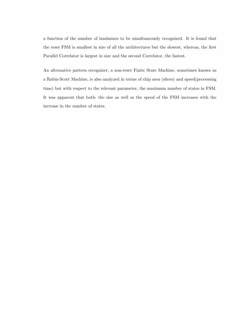
are sampled at intervals of 5 cm downrange in the direction normal to the placement of the
linear array.
Figure 2.2: An antenna penetrating the ground surface reflects a signalrepresenting a scan of 51 crossrange x 512 deep x 16-bit downrange
The sampling interval is not constant and can vary from 1-5 cm. Each antenna generates
512 sample points in depth, each bipolar sample is quantized with 16-bits of resolution
at every 1-5 cm downrange, only 12 bits of which are significant. A scan is comprised of
51(48-active) crossrange channels x 512 samples deep which forms input to the landmine
detectors being developed in this thesis.
2.2 Syntactic Pattern Recognition Theory
Every non-metallic object is comprised of materials having different electrical properties (or
dielectric constants) at certain locations. The transmit antenna radiates the RF electro-
magnetic signal (in the case of this radar, an impulse) which penetrates into the ground.

10
This signal is the electromagnetic wave that then gets reflected at the interface between
materials of different dielectric constants. The change in dielectric constant is also referred
to as impedance discontinuities.
Figure 2.3: A cross-sectional view of VS2.2 Anti-tank mine
The internal changes in impedance with range are shown in centimeters and in pixels. The
values are relative to the top of the mine and are independent of the depth under the
ground, other materials surrounding the mine such as soil or rocks and other environmental
conditions.
Figure 2.4: Change in impedance discontinuities denoted in cms and pixels

11
Whenever there is a change in impedance, there is a decrease in power due to the portion
that gets reflected back to the receiving antenna. The reflected signal is in the form of a
real-valued raw video bandwidth signal. In order to comprehend the accurate location of the
impedance discontinuity and for the data to be compatible with the landmine detectors, it is
sent through various stages of inverse filtering (degenerate Wiener filter assuming zero noise)
using pre-processing algorithms, to obtain the binary valued signal comprised of sequence
of ’ones’ and ’zeros’ where ’one’ indicates the location of an impedance discontinuity and a
’zero’, otherwise. The binarized string of data contains a specific pattern which characterizes
the structure of a mine. Every mine has a unique pattern, termed as ’string’ in a language
of mines.
Figure 2.5: A string of GPR data which consists of dithered positions,missing peaks and clutter, is compared to the Mine pattern
Due to environmental conditions and other variations, the ’one’ values can shift +/- 2
positions or pixels in either directions from the impedance discontinuity creating what
we refer to as +/- 2 dither. There may also be discontinuities missing in the string or
unexpected positions of the discontinuities recorded. They are termed as missing peaks and
clutter respectively. The language consisting of a set of strings of data, contains the strings
with dither, missing peaks and/or clutter. To recognize this language, several language
recognizers such as parallel logic implementations and finite state machines (finite automata)
are developed.

Chapter 3: Hardware Implementation on FPGA
3.1 Target Device
The device chosen to design the algorithms is the XC-5VFX70T, manufactured by Xilinx.
It is from the Virtex R©-5 family built on 65-nm triple oxide technology providing higher
density as compared to previous 90-nm triple-oxide technology of Virtex R©-4 family. The
number of logic cells available in Virtex R©-5 FPGA is 330,000, gaining 65% larger capacity
over Virtex R©-4 FPGA (200,000 logic cells). The core voltage of Virtex R©-5 FPGA has been
reduced to 1.0 Vcc from 1.2 Vcc of Virtex R©-4 FPGA, thus considerably reducing dynamic
power consumption. Every FPGA is comprised of configuration logic blocks (CLBs) and
interconnects (wires). Each CLB contains two slices within which there are 6-input LUTs
(instead of the 4-input LUT of previous generations), four flip-flops (storage elements), mul-
tiplexers and carry logic. These slices are called SLICEL. Some slices also act as distributed
RAMs or 32-bit shift registers (SRL-16 or 32). Such slices are named as SLICEM. Due to
the use of 6-input LUT, Virtex R©-5 FPGAs save significant amount of area, having 45%
less area than that of Virtex R©-4 FPGA. The diagonally symmetric interconnect pattern
(Virtex R©-5) as opposed to traditional way of interconnection (Virtex R©-4), improves the
logic performance by 30%. Virtex R©-5 FPGA maintains the balance of hardware resources
increasing the performance for computation-intensive DSP applications.
Of the five platforms (LX, LXT, SXT, TXT, and FXT) in the Virtex R©-5 family, the chosen
device uses the FXT platform which has two PowerPC 440 processor blocks with built-in
12

13
Figure 3.1: Virtex-5 FPGA Board; Device : XC5VFX70Tff1136
DMA engines, GTX/GTP transceivers for advanced serial connectivity, Tri-mode Ethernet
MACs and integrated PCI-Express (PCIe) endpoint. The device used here, takes advantage
of the PCIe x1 endpoint. As the demand for large quantity of data rises, there is a need
for higher bandwidth of the bus between PC and FPGA. This requirement is fulfilled by
PCIe endpoint having bandwidth higher than previous PCI, PCI-X devices. A x1(by one)
represents one lane made of a pair of transmit and receive signals, each uni-directional,
providing a bandwidth of 250 Mbits/s. Since this is a serial I/O bus, it allows both the
signals to transfer the data on the lane simultaneously, achieving a total bandwidth of 0.5
Gbits/s. The on-chip PowerPC 440’s are not used in the laboratory demonstration work
documented here but could be used in a deployable system.
3.2 FPGA Hardware Programming
Though Virtex R©-5 FXT devices are suitable for both, Windows as well as Linux operating
systems (OS), Xilinx ISE 10.1i tool works only on Windows R© OS. Also, the devices work
with either 32-bit or 64-bit machine with 1-2GB system memory.
14
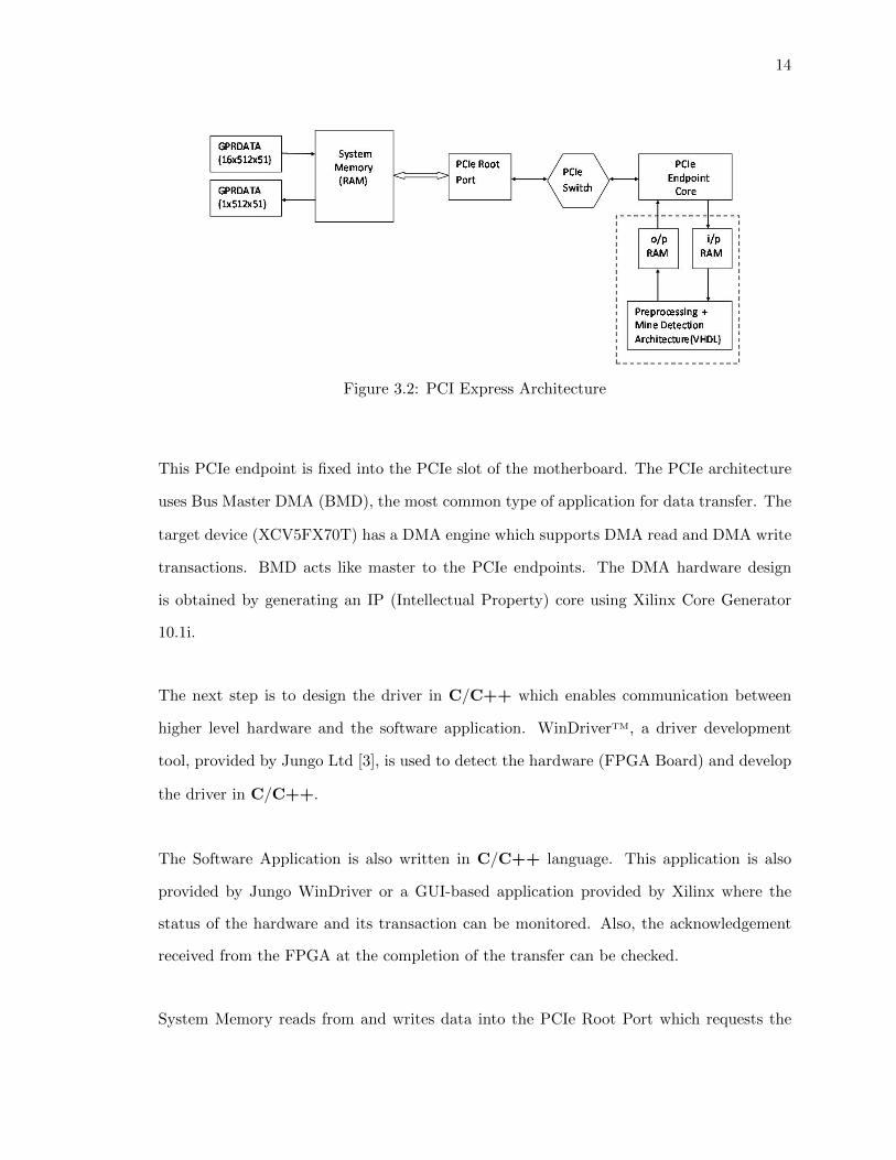
Figure 3.2: PCI Express Architecture
This PCIe endpoint is fixed into the PCIe slot of the motherboard. The PCIe architecture
uses Bus Master DMA (BMD), the most common type of application for data transfer. The
target device (XCV5FX70T) has a DMA engine which supports DMA read and DMA write
transactions. BMD acts like master to the PCIe endpoints. The DMA hardware design
is obtained by generating an IP (Intellectual Property) core using Xilinx Core Generator
10.1i.
The next step is to design the driver in C/C++ which enables communication between
higher level hardware and the software application. WinDriverTM, a driver development
tool, provided by Jungo Ltd [3], is used to detect the hardware (FPGA Board) and develop
the driver in C/C++.
The Software Application is also written in C/C++ language. This application is also
provided by Jungo WinDriver or a GUI-based application provided by Xilinx where the
status of the hardware and its transaction can be monitored. Also, the acknowledgement
received from the FPGA at the completion of the transfer can be checked.
System Memory reads from and writes data into the PCIe Root Port which requests the

15
transaction to the PCIe Switch via BMD channel. The PCIe switch is connected to various
PCIe endpoints. The PCIe Endpoint Core which is nothing but the hardware design written
in VHDL includes the BMD design. Input RAM and output RAM is included to read data
from and write data to preprocessing and landmine detection algorithms. The output data
is sent back to the system memory for the user to read it in the application program.
The FPGA chip on the board is programmed using either a ACETM CompactFlash card or
a Xilinx Parallel Cable IV through JTAG Port.
3.3 FPGA Design Tools
The two novel architectures discussed here are coded in VHDL using the algorithmic state
machine method. This method supports top-down hierarchical design. The method consists
of controller and datapath. The controller controls the signals from and to the datapath
and also between the datapath and the external interface. The datapath usually contains
a combinational logic. The controller is created with the finite state machines using Moore
and Mealy type machines. This method of designing the architectures gives a systematic
approach in performing the detection.
The entire design including the BMD design is implemented in Xilinx ISE 10.1i software.
The design is first put to test by functional simulation using test-bench also written in
VHDL. The ModelSim SE 6.5c environment aids in debugging the design and analyzing the
waveforms. Even if the design is simulated successfully, it only verifies the syntax and the
logic of the design, but it has to fulfill the hardware requirements on the FPGA. For this
reason, it is synthesized using XST (Xilinx Synthesis Tool) tool where high level synthesis
creates a netlist and checks the hierarchy of the entire design architecture . The low level
synthesis gives the distribution of the logic gates and flip-flops on the FPGA.

16
The design is then mapped on the actual internal architecture of the FPGA and pack-
ing and placement of the resources takes place during the implementation process. The
implementation process then runs place and route which places the CLBs and routes the
interconnects appropriately and also checks the timing constraints. The next step in the
process is creating the bitstreams which are then downloaded onto the FPGA using Xilinx
iMPACT 10.1i tool.

Chapter 4: Previous Research
The pre-processing algorithm implementation was designed by J. Corey Wright and is docu-
mented in his Master thesis in [1]. This algorithm does not impact the results of this thesis,
therefore, there was no need to re-work this part of the project. But the pre-processing
cannot be neglected either, for it plays a certain role in calculating the speed or the pro-
cessing time of the entire detection methodology. He also designed two syntactic landmine
detection algorithms- a parallel correlator having large size but faster in speed and a serial
finite state machine (Major/Minor FSM) with smaller size but slower speed. Since these
three algorithms are described in [1] in detail, this chapter only gives a brief description of
the stages involved in this preprocessing methodology and the architectures employed for
the pattern recognition techniques.
4.1 Preprocessing Algorithm
The preprocessing algorithm is used to improve the spatial resolution of the GPR returned
raw video signal and convert it into the binary valued data. The samples were carried out
with only 24 antennas and 417 points in depth in J. C. Wright’s work as that was the
original design of the Wichmann antenna. Nothing in these results affects the current 51
channel design as the processing is on a per channel basis.
The GPR returned signal is a bipolar signal of different amplitudes. The bipolar signal
is processed to locate the impedance discontinuities more precisely. This is performed with
the help of inverse filters (1-D convolution kernel) known as 1-D inverse filtering.
17

18
Figure 4.1: Preprocessing Algorithm ([1])
Due to the antennas arranged in a form of linear array in a crossrange, adjacent antenna
crosstalk is observed. The wide beamwidth of the antennas make the signal appear like a
hyperbola rather than a point in both crossrange and downrange directions. In order to
reduce the depth and crossrange spreading, a sphere is placed in front of the GPR and is
then 1-D inverse filtered. This range filtered signal is then used to develop a 2-D inverse
filter for improving the signal to noise ratio. This straightens out the signal obtaining an
improved measurement of the physical structure of a landmine. This process is called 2-D
inverse filtering.
4x1 average filtering and rectangular LPF filtering is carried out to reduce the effect of noise.
The processed signal is then absolute valued so that all the amplitudes are represented as the
positive indicators. A suitable threshold is set so as to designate all the amplitudes above
this threshold to be the location of impedance discontinuities, eliminating other unwanted
amplitudes considering them as clutter. The peak detection process converts this signal
into binary format of 1’s and 0’s where 1’s indicate the location of impedance discontinuity
and 0’s indicate the absence of it. A binary scan of 51 x 512 x 16-bit data is assumed to be
obtained at the output of this algorithm.

19
This design was implemented on Virtex-4 device XC4VSX55-12 using Xilinx System Gen-
erator which is in the Matlab’s Simulink toolbox. The GPR scan processing time was
calculated by J. C. Wright to be 0.463 seconds/scan (with 24 channels x 416 deep samples
of scan), that is, at 1 cm downrange, it achieved the speed of 4.83 miles per hour. It is
observed that only 25% of the device was utilized. Hence, if Virtex-5 device is considered
for the implementation of the same design, fewer slices would be utilized and also the time
to process a scan would be faster. The nominal speed of advance is currently 5 cm/sample
leading to a 5-fold increase in the speed of the vehicle, still within the capabilities of the
current processing speed.
4.2 Landmine Discrimination
The landmine discrimination techniques described below, aid in the detection of any mine
pattern of interest of arbitrary length. Both the methodologies are based on the concept of
loading both the strings, GPR data and a mine pattern of interest, into the detector and
calculating the number of missing discontinuities and clutter errors detected while matching
the impedance discontinuities.
4.2.1 Reset Finite State Machine
This is a reset finite state machine which involves a major FSM and a minor FSM. The
minor FSM performs the actual determination of the depth at which there is a match in the
impedance discontinuities in a mine pattern and a GPR data, a number of missing errors
and clutter errors encountered. Whereas the major FSM ensures if the missing errors and
clutter errors are within the required threshold level and decides if the final state reached
is in an accept state or a reject state (if threshold exceeds).

20
Figure 4.2: Architecture of Reset FSM ([1])
FSM is the serial processor, that is, the GPR data is read serially, bit by bit, into the
detector. A storage memory is the state transition matrix that has the present state and
the next transition state that depends on the match between GPR data and mine pattern.
Every bit of the GPR data is compared with every bit of mine pattern and the pair of
the bits is the pointer to the address of the state transition matrix. At the end of the
mine pattern, when the last pair is read, the state decoder deciphers the detection and also
determines the depth at which the mine is located.
4.2.2 Parallel Correlator
The parallel set of single bit correlators are deployed in this parallel logic implementation.
Like FSM, the logic makes sense only when the most significant bit (MSB) of the landmine
data is ’1’. Unlike FSM, this correlator is loaded in parallel into the detector. The length
of GPR data extracted from the entire string of 512-bit data equals the length of the mine

21
Figure 4.3: Architecture of Parallel Correlator ([1])
pattern. Each position of the GPR data is matched with that of the mine pattern. Whenever
there is no match, there is either missing discontinuity or the clutter.
Unlike the FSM implementation, the correlation approach is entirely implemented in com-
binational logic with no feedback path or storage.
Due to the +/- 2 dither positions, occasionally, when finding the match between the GPR
data and mine pattern, a case can occur when ’1’ in the GPR data is in such a position
that it can be either associated with the 1 which is located two positions before and after,
in the mine pattern. Here, setting the priority becomes a major concern. Hence, the logic
used to calculate the location of the mine, the number of missing errors and clutter error is
based on the priority dither masking operations.
22
4.3 FPGA Implementation
The input to the above detectors was a scan of 24 channels x 417 deep x 1-bit downrange
and both of the detectors were implemented using Virtex-4 device XC4VSX55-12. Since,
these architectures are to be compared with the hard-coded parallel correlator which uses
a Virtex-5 device for implementation, it had to be re-synthesized and re-implemented using
Virtex-5 device XC5VFX70T-1 with the input data to be a scan of 51 channels x 512 deep
x 1-bit downrange. The data into the detectors is processed on scan-by-scan basis. Also,
the maximum length of mine pattern considered in the existing architectures is 100 whereas
the one required in this thesis is 128.
Those modules which use a significant amount of area are taken into consideration and
every sub-module is mapped individually to get the idea of the slice distribution.
4.3.1 Reset Finite State Machine
Table 4.1: Slice Distribution of different modules of the Reset FSM
The Critical Path Delay of FSM is 3.755 ns. The latency of the circuit to process one scan
of 512 depth is (MINE LENGTH+2)x GPR LENGTH cycles where 2 is the allowed dither.
In this case, the MINE LENGTH of 128 gives the latency of 128 x (512-128+1) cycles and
23
that is 49,280 x clock period = 49,280 x 3.755 = 185.05µs of scan processing time.
4.3.2 Parallel Correlator
Table 4.2: Slice Distribution of different modules of the Parallel Correlator
The Critical Path Delay of Parallel Correlator is 73.86 ns. The Latency of the circuit is
(GPR LENGTH - (MINE LENGTH - 1)) + 4 = 389 cycles where, additional 4 clock cycles
are for the initial pipelining delay. The processing time of a scan is thus, 28.73µs. The
size and speed of both the architectures are dependent on the length of the mine pattern,
though it is independent of the impedance discontinuities present in the mine pattern. The
dependency could be observed in [1] in more detail.
4.4 Modified Algorithms
The two existing architectures are designed for the purpose of detecting just one mine
pattern of interest at one time. Here, the scope of these designs is extended such that they
are able to perform the detection of multiple mines simultaneously. Since, these original
architectures are flexible to detect a mine of any length or type, the same hardware resources
are made to share for detecting any mine pattern of interest loaded into the detector. All
24
the mine patterns, since loaded in parallel, are made to match simultaneously with the GPR
data of 512-bit which is also loaded in the same detector.
In the case of the Parallel Correlator, the priority dither masking operations of all the mine
patterns are performed in parallel and hence, the detection of each mine along with the
determination of missing errors and clutter errors for each mine are executed. In the case
of the Finite State Machine, a state transition matrix is generated based on the paired bits
of GPR data and mine pattern. Hence, all the mine patterns loaded into the detector is
paired with a single GPR data and the state transition matrix is read. Ultimately, the mine
pattern is detected and the missing errors and clutter errors are determined for each mine
pattern simultaneously.
4.4.1 FPGA Implementation
Since the same logic is used to perform the detection of one landmine as any other landmines,
the whole design is instantiated the number of times the mine patterns are to be detected.
The different mine patterns of interest at the input side are to be loaded into the detectors
and separate output files are written to comprehend the exact results for every mine pattern
loaded.
Also, because one and the same logic is used for all the mine patterns, same hardware
resources are shared and do not need to be replicated therefore, the hardware resources
utilized on Virtex-5 FPGA chip are exactly the same for any number of the landmines
taken into consideration. Hence the size and the speed mentioned in the earlier section
remain unchanged.

25
Figure 4.4: Slice Distribution of different modules of the Reset FSM
Therefore, the graph of slices and critical path delay would be uniform over the number of
mines to be detected.

26
Figure 4.5: Slice Distribution of different modules of the Parallel Correlator

Chapter 5: Hard-Coded Parallel Correlator
The hard-coded parallel correlator (HCPC), a behavioral equivalent of the parallel correlator
which has already been discussed, is based on the similar concept of deploying set of single
bit correlators. The output of the HCPC specifies the impedance discontinuity spacing that
defines a unique landmine. The detector, as the name goes, is hard-coded for a particular
mine pattern of interest, as opposed to the previous correlator which was made generic for
any type of mine of any length. The mine detection logic includes a language recognizer
and the noise detector.
Figure 5.1: Concept of Hard-Coded Parallel Correlator
The length equal to the length of the mine pattern is extracted from the 512-bit GPR data.
The detection logic makes sense only when the start bit of the input data is ’1’. In bank
27

28
of correlators, the MSB(most significant bit) of the input string is ANDed with the every
other bit for (MINE LENGTH-1) bits. The output of the correlators, as shown in Figure
5.1, is the sequence with the impedance discontinuities and its dithered counterparts. To
verify that one and only one impedance discontinuity is present at the expected position or
at +/- 2 dithered positions, the language recognizer makes use of 5-bit XOR. The number
of 5-bit XORs depends on the number of the impedance discontinuities present in the mine
pattern.
Though each positions of the impedance discontinuity in the GPR data match for each
discontinuity in the mine pattern, the other positions in GPR data must be checked for it
should not contain more than two positive indicators. More number of positive indicators
result into clutter and not a landmine. These indicators are considered as noise pulses in
the input data. A noise detector contains the logic that detects the presence of noise pulses.
It consists of two modules: One, where all the bits are ORed and it is checked if no or ’0’
noise pulse is present. The other module checks if ’1’ or more noise pulses are present in
the input data. Not more than one noise pulse is allowed for a mine detection to take place.
5.1 Architecture
The 3-D processed GPR scan of 51 crossrange x 512 depth x 1-bit downrange is stored into
the FPGA memory of 32,768 x 1-bit Block RAM. Since the operation on the data takes
place in parallel, the n-bit data (where n is the length of mine pattern) is read serially into
the detector and is first converted into parallel data in the Serial to parallel converter. The
n-bit parallel data is fed into the Mine Detection Logic.
This logic first checks the correlation between the input string and the mine pattern. Then,
the language recognizers detect the location of impedance discontinuities. As discussed

29
Figure 5.2: Architecture of Hard-Coded Parallel Correlator
earlier, the noise detector decides if the input string is a landmine or a clutter. The table
below indicates the output of noise detection:
Noise pulse ’0’ = 1, when noise pulse > 0;
= 0, when noise pulse = 0;
Noise pulse ’1’ = 1, when noise pulse = 1;
= 0, otherwise;
Table 5.1: Truth Table of noise detector
Depth and Cross-range counters set the limit for the entire GPR scan to be read at a time.
The control logic introduces required delays, controls the signals of the counter, enables

30
shifting of the data in the serial to parallel converter and controls the read-write signals of
the Block RAMs. The output of the mine detection logic is a detection bit for every string
operated, which is stored in the detection memory of 32,768 x 1-bit Block RAM indicating
the channel and the exact depth at which the landmine is located.
5.2 FPGA Implementation
The HCPC was designed using synthesizable VHDL code in Xilinx ISE 10.1i and was
synthesized and implemented in XST tool using XC5VFX70Tff1136-1. There is no specific
goal for optimization, but optimizing for area does not make much of a difference in the size
of the design. This design is optimized for speed. The modules are mapped to comprehend
the slice distribution and also the contribution of each module in its utilization of the
resources.
Table 5.2: Area utilization of HCPC
The area on the FPGA is mainly utilized by the mine detection logic. Though there are
as many language recognizers as there are impedance discontinuities, the LUTs utilized by
language recognizers are very negligible. The design depends largely on the length of the
mine pattern.

31
The slice utilization increases proportionally with increase in the length of the mine pattern.
The 128- bit serial to parallel converter usually uses 128 registers. However, in some cases,
XST tool maps the serial to parallel converter onto SRL32 primitive, dedicated slice for shift
registers. This considerably aids in the reduction of the number of flip-flops and LUTs, but
at the cost of delay. This, can be seen in the graphs below in Figure 5.3, when the length of
mine pattern is 82 and 200. Hence, the speed is greater for a mine length of 82, decreases
at lengths of 100 and 128 and again increases significantly at 200.
For the correlation data, 100 AND gates are used and for noise detectors to detect ’0’ or
’1’ noise, use OR gates and XOR gates. There are also few multiplexers and comparators
which are very few in number. The maximum delay is formed in the input and the
output RAMs due to use of 15-bit and 16-bit address counters . Hence, if these modules are
excluded for the time being in order to observe the actual module consuming the delays,
the critical path is observed to be in the mine detection logic which only has combinational
path delay of around 8.516 ns . The critical path delay of the overall system achieved,
including the RAMs, is 5.707 ns. The latency of the parallel correlator is GPR LENGTH
x (MINE LENGTH - 1) = 512 x (128 - 1) = 385 cycles. Hence, the scan processing time
is 385 x 5.707 ns = 2.20µs. This is the time a detector takes to process one scan of 51
crossrange x 512 deep x 1-bit.
Following are certain observations regarding the dependency on the length of the mine
pattern on the area and speed of the correlator.
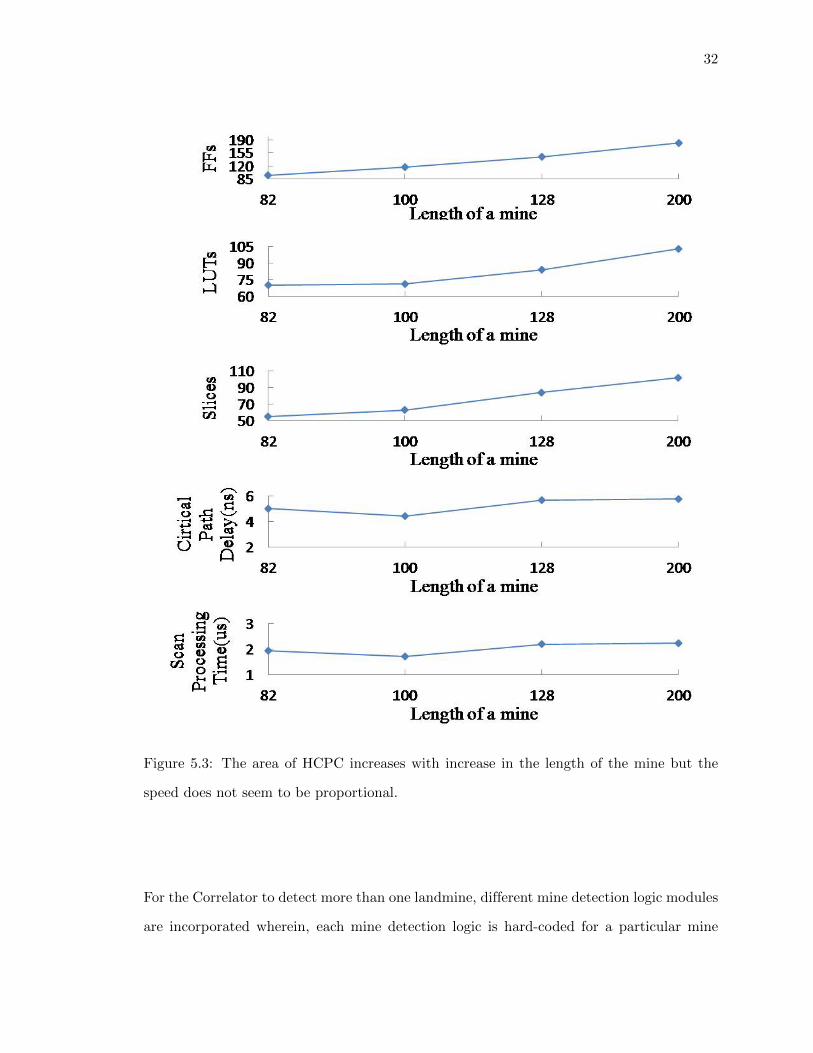
32
Figure 5.3: The area of HCPC increases with increase in the length of the mine but the
speed does not seem to be proportional.
For the Correlator to detect more than one landmine, different mine detection logic modules
are incorporated wherein, each mine detection logic is hard-coded for a particular mine

33
pattern of interest. There are as many mine detection logic modules added as there are mine
patterns to be detected. This allows for the detection of the multiple mines simultaneously.
Also, other hardware resources like counters, shift registers and control logic are shared,
since the operations are performed on a single scan of GPR data. Also, the Detection RAMs
are added for storing the detection results for each of the mine patterns being detected.
Since the size and speed of the design depends on the length of mine pattern, the same
mine length of 128-bits is considered for consistency. Following is the table for the total
utilization of the resources as a function of number of the mine patterns to be detected.
Table 5.3: Area utilization by HCPC as a function of the number of mines to be detected

34
Figure 5.4: The area of the HCPC increases but the speed remains almost the same with
increase in the number of mines to be detected

35
It is observed that as the number of mine patterns to be recognized is increased, though
the hardware resources utilized increase proportionally, the speed of all the correlators is
comparable. The average critical path delay thus, calculated is 6.085 ns. The time it takes
to process one scan is on average 2.34µs.

Chapter 6: RAM Based Finite State Machine
As discussed earlier, a binary string of data, or a column of processed GPR data, consists of
several impedance discontinuities, missing peaks and noise pulses. Also, there is a dither of
+/- 2 locations before and after the expected position of an impedance discontinuity in this
landmine. To locate a mine pattern in a string of GPR data, a detector has to detect a mine
from various patterns caused by dithering, missing peaks and noise pulses. For example, if
there are K impedance discontinuities in the mine pattern of length n, the dither is denoted
as d and the noise pulse is denoted as J, the total number of patterns to be recognized by
the detector is given by the equation1[4],
N(u)mine = (2d+ 1)K
J∑j=0
(n− (2d+ 1)K − 3)
j
)
This equation is calculated with no missing peaks. If there are P missing peaks considered,
then there will be(
KK−P
)· N (u)
mine patterns in addition to N(u)mine patterns. These patterns
which are formed due to dither and also due to missing peaks and noise pulses are an
example of an enumerated language, or a regular language. Finite State Machines are the
class of machines which are able to recognize this language. More complicated machines,
such as push down automata or Turing machines are not required.
1
(n
k
)=
n!
k!(n− k)!
36

37
Efforts were taken by S.Chetlur-Kannan to design the FSM maker program using the C
language. Her program produces a state transition matrix and a final state matrix. A state
transition matrix is a two-dimensional matrix having columns which contain the next state
based on the input ’0’ or ’1’ with the row address being the present state. The final state
matrix is a single column matrix containing zeros and non-zero values. Non-zero values
indicate a presence of a mine or an acceptance state and zeros indicate a reject state.
The matrices define the maximum number of states required by the FSM to detect all the
possible patterns of a particular mine. The FSM generator is dependent on the length as
well as on the number of impedance discontinuities present in the mine pattern. Since, the
FSM generator is hard coded for a particular mine, it has to be run every time the new
pattern is to be detected.
A language recognizer, also known as Robin-Scott Machine, as designed by Dr. K. J. Hintz,
in MatlabTM and is now hardware implemented using VHDL for making it viable for real-
time applications. The language recognizer is a non-reset finite state machine which allows
for the detection of a landmine string embedded in a longer string of clutter. Even after the
recognizer has reached the acceptance state, the non-reset FSM continues to operate even
if the process is in the middle of the string and does not need to reset and go back to the
start state.
Figure 6.1: A state transition depends on the input and present state
The concept of this FSM is that while in the present state, the FSM makes the transition

38
to the next state based on the input whether its ’0’ or ’1’ bit and outputs the final state to
decide whether it is in the acceptance state or the reject state.
6.1 Architecture
A three-dimensional scan of 51 crossrange x 512 depth x 1-bit downrange is stored into
the Block RAM of size 32,768 x 1-bit on FPGA. Each channel is being operated into the
recognizer one by one. The string of length of that of the mine pattern is read into the shift
register of n-bit, where n = 128. The 512-bit of data is processed serially bit by bit into
mine detection logic.
Figure 6.2: Architecture of RAM-based FSM
Mine detection logic instantiates two storage elements, a state transition matrix, known as
Delta matrix, and the final state indication matrix, referred to as FSIM, are stored in the
block RAMs. The FSM is in the reset mode until the start bit in the input is read as ’1’.
This is the pointer to the address of the delta RAM. The transition to the next state takes
place based on the next bit read at the input data. The first column in the Delta matrix is
considered as a next state if ’0’ is read at the input data and the second one is considered,
if a next bit is ’1’. The next bit of the delta matrix is a pointer to the address of the FSIM
39
RAM. Once the n-bit of the input data is read, the detector checks the values in the FSIM
memory. It has values ranging from 0 to 5.
THRESHOLD = 5 - MISSING PEAKS - NOISE PULSES
The non-zero value read from the fsim RAM must be greater than or equal to the set
threshold value. This determines if the mine is said to be in the acceptance state or a reject
state. The detection bit at every depth is recorded into the detection RAM of size 32,768
x 1-bit Block RAM.
Depth and Cross-range counters set the limit for the entire GPR scan to be read at a
time. The control logic introduces required delays, controls the signals of the counter,
enables shifting of the data in shift registers and controls the read-write signals of the Block
RAMs.
6.2 FPGA Implementation
The FSM is designed using synthesizable VHDL code in Xilinx ISE 10.1i and is synthesized
and implemented in XST tool using XC5VFX70Tff1136-1. This design is optimized for
speed. The modules are mapped to comprehend the slice distribution and also the contri-
bution of each module in its utilization of the resources. The length of mine pattern under
test is considered to be 128.
Here, since the shift register is read out serially, the entire n-bit does not get operated
simultaneously. Therefore, instead of using 128 registers, the shift register is mapped onto
the SRLC32E primitive, a dedicated slice register for shift registers (SLICEMs). Four LUTs
and Four LUTRAMs (SLICEMs) and only one SLICEL are utilized on FPGA instead of

40
Table 6.1: Area utilization of RAM-based FSM
128 flip flops and 32 slices. This saves the flip-flop and slice utilization considerably, though
compromising on the delay.
There are few comparators, multiplexers being utilized. The control logic module is syn-
thesized as a finite state machine. Mine detection logic is the only module significantly
contributing to the slices utilized on the FPGA.
The FSM is completely independent of the number of impedance discontinuities present in
the mine pattern, unlike the FSM maker. Also, the design is made independent of length
of the mine pattern. However, the overall size and speed of this architecture is controlled
by and is measured in terms of the maximum number of states the FSM takes to detect all
possible patterns of the mine pattern. This number of states defines the size of the block
RAM in which delta matrix and FSIM matrix are stored. Block RAMs are used instead
of ROMs for the requirement of large storage capacity to accommodate at the most 65,536
states of FSM and lack of availability of ROMs on the Virtex-5 FPGA chip.
Size of Delta RAM = (Number of bits representing the next state x 2) x Number of States
Here, half of the bits indicate the next state in the transition when the input is ’0’ and

41
latter half of the bits indicate the next state when the input is ’1’. Start state of the delta
matrix is always 1.
Size of FSIM RAM = (Number of bits representing the final state) x Number of states.
Here, three bits are required to represent the final state.
In Virtex-5 FPGA, there are two block RAM primitives, RAMB18 and RAMB36. RAMB18
can take maximum of 18-bit of port width and RAMB36 can take up to 36-bit of port
width. Also, 36-bit port width is split into 32-bit input/output bus + 4-bit parity bus.
Hence maximum of 32-bit data width could be used in this design. Therefore, Delta RAM
can take up to 16-bits to represent a FSM state, that is, maximum of 216 = 65,536 number
of states this design can occupy.
The following table provides the total number of BRAMs utilized and the critical path delay
of the FSM as the number of states increases. Each design has 32,768 x 1-bit input and
output RAMs which takes up to 2 RAMs. Every block RAM used in the design is mapped
onto RAMB36 primitive which has maximum size of 1K x 36.
Table 6.2: Utilization of BRAMs as a function of number of states in FSM
The maximum delay is contributed by the mine detection logic and the critical path is from
input of the Delta RAM to the another input of that RAM which is the pointer to the
address of the next state with the delay of 9.782 ns . This is again excluding the input and
42
output RAMs which are the actual modules consuming the delays due to the use of 15-bit
and 16-bit address counters. In finite state machine, the latency and the scan processing
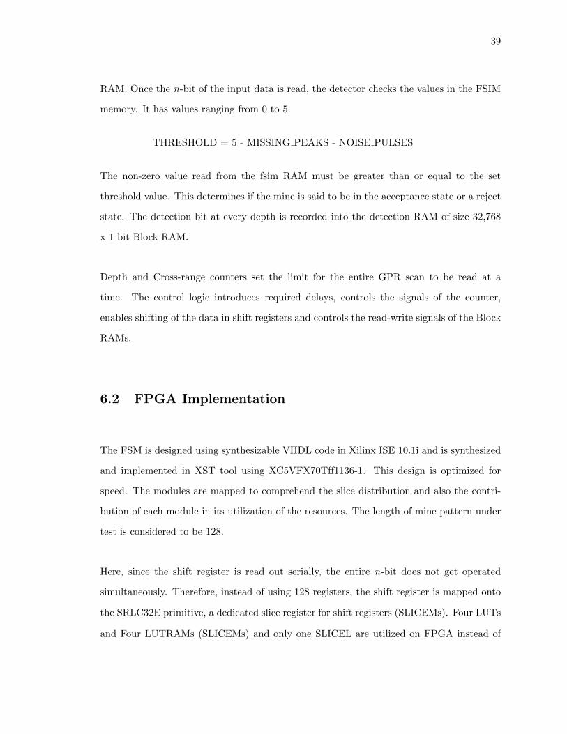
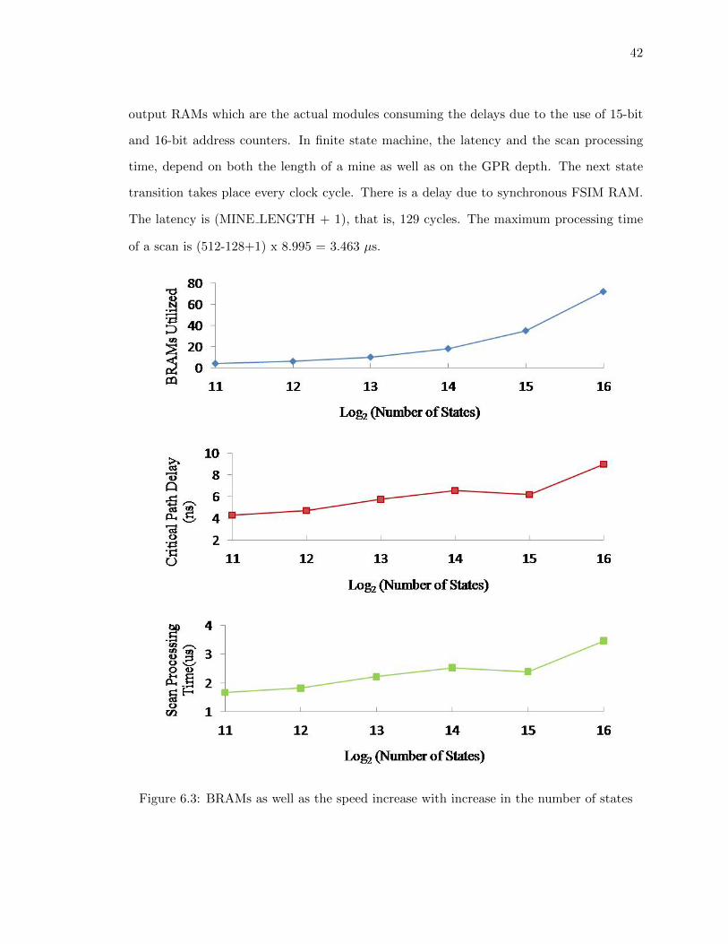
time, depend on both the length of a mine as well as on the GPR depth. The next state
transition takes place every clock cycle. There is a delay due to synchronous FSIM RAM.
The latency is (MINE LENGTH + 1), that is, 129 cycles. The maximum processing time
of a scan is (512-128+1) x 8.995 = 3.463 µs.
Figure 6.3: BRAMs as well as the speed increase with increase in the number of states

43
The size and speed of the FSM does not change as the number of states goes below 4,096.
In figure 6.3, the curve of the utilization of the BRAMs clearly shows its proportionality
with the number of the states. The curve of the critical path delay also shows the increase
in speed with the increase in number of states.

Chapter 7: Conclusion and Scope
7.1 Conclusion
The two modified architectures, the reset FSM and a parallel correlator, and two novel
architectures, hard-coded parallel correlator and RAM-based non-reset FSM, are described
in this thesis. The mine patterns used to test the detectors are just exemplars (not true
mine patterns are put under test). The length of the mine pattern (128) considered is the
maximum of all the known mine patterns.
The HCPC, like the previous two detectors, is dependent on length of landmine and also,
barely dependent on number of impedance discontinuities present. Whereas the RAM-
based FSM is made independent of the length or the number of impedance discontinuities
of the mine pattern of interest.
It is observed from the following graphs, Figure 7.1, that area utilization is highest in the
first Parallel Correlator and the areas of other the two architectures are nearly the same.
The following is the order of their area utilized on chip from smallest to largest.
Reset FSM Û Hard-Coded Parallel Correlator Û Parallel Correlator
However, the speed, that is, the scan processing time is shown in the order from fastest to
slowest.
44

45
Hard-coded Parallel Correlator Û Parallel Correlator Û Reset FSM
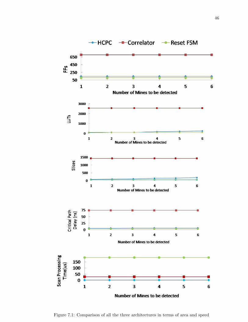
46
Figure 7.1: Comparison of all the three architectures in terms of area and speed

47
The speed the HCPC is the fastest and reset FSM is the slowest.
In case of the RAM based non-reset FSM, it is apparent that both the size and the speed
of the FSM increases proportionally with the number of states with FSM.
7.2 Scope and Suggestions
The slice utilization of the hard-coded Parallel Corrselator (HCPC) to detect 6 landmines
is hardly about 2%. Hence, the same architectures of parallel correlators and reset FSM
can be extended for detecting 12 or more (up to 300) landmines.
Since the GPR used is presumed to have a very low false alarm rate, the input GPR data
should not contain more than two noise pulses. If it does, the noise detector would fail and
HCPC would falsely determine the detection of the landmine. Hence, the correlator is to
be designed to detect the landmine accurately even when there are more number of noise
pulses present in the data. The algorithm for such correlator would be more complex and
would require large number of sequential circuits rather than simple combinational logic
circuits introducing large delays. Such design is out of the scope of this paper.
The FSM Maker defining the number of states could produce FSM with upto 5 million
states. However, this could be implemented on hardware since the data goes beyond the
capacity of Virtex-5 FPGA used in this thesis. In order to achieve this goal, just increasing
the external block RAMs for storing the matrix elements would not work, since they would
still have the limitation on their data bus width of 32-bits.

48
Appendix A: Appendix
The next state transitions are based on the concept provided in the figure below. The final
states are reached at 20,22,8,12 and 17. These states define different patterns formed out
of a mine pattern 1000100.
Figure A.1:Concept of FSM Maker [5]

Bibliography
49
50
Bibliography
[1] J. C. Wright, “Pattern Recognition Implementation Comparison with Applications forMine Detection in GPR,” MS Thesis, George Mason University, Aug. 2006.
[2] S. Chetlur-Kannan, “Landmine Detection Using Syntactic Pattern Recognition,”MSEE Scholarly Paper, George Mason University, Nov. 2004.
[3] http://www.jungo.com/st/windriver driver development pci express.html.
[4] A. O. Nasif, B. L. Mark, K. J. Hintz, and N. Peixoto, “Upper bound on false alarm ratefor landmine detection and classification using syntactic pattern recognition,” GeorgeMason Univeristy.
[5] S. Chetlur-Kannan, “Landmine detection using syntactic pattern recognition,” presen-tation slides, George Mason University, Nov. 2004.
[6] K. J. Hintz, “High speed syntactic landmine detection and classification,” Dec. 2007.
[7] K. Hintz, “High speed mine classification,” Jun. 2007, slides briefing presented toBooze-Allen-Hamilton.
[8] K. J. Hintz, “SNR improvements in NIITEK ground penetrating radar,” Detectionand Redmediation Technologies for Mines and Minelike Targets IX;Russell S. Harmon,J.Thomas Broach, John H. Holloway, Jr.;Eds, Proc. SPIE, vol. 5415, pp. 399–408, Apr.2004.
[9] K. J. Hintz and T. Desai, “A parallel implementation of lms adaptive filter in hard-ware for landmine detection,” Detection and Redmediation Technologies for Mines andMinelike Targets IX;Ruseell S. Harmon, J.Thomas Broach, John H. Holloway, Jr.;Eds,Proc. SPIE, vol. 5415, pp. 973–983, Apr. 2004.
[10] T. Desai and K. J. Hintz, “Volumetric signal processsing hardware acceleration for minedetection,” Detection and Redmediation Technologies for Mines and Minelike TargetsIX;Ruseell S. Harmon, J.Thomas Broach, John H. Holloway, Jr.;Eds, Proc. SPIE, vol.5089, pp. 863–871, Apr. 2003.
[11] K. Hintz, “Syntactic landmine detector,” U.S. Patent 7,320,271, Jan., 2008.
[12] S. Chetlur-Kannan, “FSM dither ver1.pdf,” Aug. 2004.
[13] http://www.niitek.com.

51
[14] http://www.xilinx.com.
[15] Virtex-5 Family Overview.
[16] Virtex-5 FPGA User guide.
[17] Virtex-5 FPGA Integrated Endpoint Block for PCI Express Designs User Guide.
[18] ML505/ ML506/ ML507 Evaluation Platform User Guide.
[19] ML507 PCIe x1 Endpoint Design.
[20] LogiCORE Endpoint Block Plus for PCI Express User Guide.
[21] XAPP1052- Bus Master DMA Performance Demonstration Reference Design for theXilinx Endpoint PCI Express Solutions.
[22] http://www.mineaction.org.
[23] http://www.landmines.org.
[24] “Landmine monitor report 2009- toward a mine-free world,” http://www.icbl.org, 2009.
[25] J. Zhang and B. Nath, “Processing and analysis of ground penetrating radar landminedetection,” Melbourne, Australia, 2004.
[26] J. Houston, “Landmine detection with a standoff acoustic/laser technique,” Aug. 2008.
[27] J. MacDonald and J. R. Lockwood, “Alternatives for landmine detection,” 2003.
52
Curriculum Vitae
Nikita Charankar received Bachelors of Engineering in Electronics and TelecommunicationEngineering from Rajiv Gandhi Institute of Technology, University of Mumbai, Mumbai,Maharashtra, India in 2006. She worked for ZTE Telecom India Ltd. as a Telecom Engi-neer. She came to USA to pursue Master of Science in Electrical Engineering at GeorgeMason University in Fall 2008. She was a Teaching Assistant in Electrical and ComputerEngineering Department. She was also a Research Assitant and was involved in the researchproject related to landmine detections sponsored by Office of Naval Research (ONR).