Lab6 FSK Modulator
5
LAB 6 – BINARY FREQUENCY SHIFT KEYING (BINARY FSK) MODULATOR 1. In troducti on Frequency shift keying (FSK) is a relatively simple, low-performance form of d igital modulation. Binary FSK is a form of F SK where the input signal can have only two different values (hence the name binary). Binary FSK is a constant-envelope form of angle modulation similar to conventional frequency modulation except that the modulating signal varies between two discrete Voltage levels (i.e., l’s and 0’s) rather than with a continuously changing value, such as a sine wave. Binary FSK is the most common form of FSK. With Binary FSK, the center or carrier frequency is shifted (deviated) by the binary input signal. Consequently, the output from an FSK modulator is a step function in the frequency domain. As the binary input signal ch anges from a logic 0 to a logic 1 and vice versa, the FSK output signal shifts between two frequencies; a mark or logic 1 frequency and a space or logic 0 frequency. In this experiment, the XR- 2206 monolithic function generator is used for the FSK modulator. 2. Mater ials Required Equipment 1 - protoboard 1 dual dc po wer supp ly(+l2 Vdc a nd - 1 to +3 Vdc ) 1 - medium frequency function generator (100 kHz) 1 - standard oscilloscope (10 MHz) 1 - assortment of test leads and hookup wire Parts List 1 XR-2206 function generator 1 47-k Ω resistor 3 4.7-k Ω resistors 1 1-k Ω variable resistor 1 8.2-k Ω resistor 2 0.001 µF capacitor 1 12-k Ω resistor 2 1 µF capacitors 1 33-k Ω resistor 1 10 µF capacitor 3. Pre- lab Bring the XR-2206 data sheet to the lab session. In the Frequency Sweep and Modulation section of the data sheet, find and record the equation for the theoretical frequency of operation, f , as a function of R, C , R C , and V C . (Note that the components have different designations in Circuit 1, below.) In the FSK Generation section of the data sheet, find and record the equation for the theoretical frequencies, f 1 and f 2 , as a function of R 1 , R 2 , C , and the FSK input Voltage.
-
Upload
anonymous-cduzmzjq73 -
Category
Documents
-
view
213 -
download
0
Transcript of Lab6 FSK Modulator

7/30/2019 Lab6 FSK Modulator
http://slidepdf.com/reader/full/lab6-fsk-modulator 1/5
LAB 6 – BINARY FREQUENCY SHIFT KEYING (BINARYFSK) MODULATOR
1. Introduction
Frequency shift keying (FSK) is a relatively simple, low-performance form of digital
modulation. Binary FSK is a form of FSK where the input signal can have only twodifferent values (hence the name binary). Binary FSK is a constant-envelope form of angle modulation similar to conventional frequency modulation except that the
modulating signal varies between two discrete Voltage levels (i.e., l’s and 0’s) rather than
with a continuously changing value, such as a sine wave. Binary FSK is the mostcommon form of FSK. With Binary FSK, the center or carrier frequency is shifted
(deviated) by the binary input signal. Consequently, the output from an FSK modulator is
a step function in the frequency domain. As the binary input signal changes from a logic0 to a logic 1 and vice versa, the FSK output signal shifts between two frequencies; a
mark or logic 1 frequency and a space or logic 0 frequency. In this experiment, the XR-
2206 monolithic function generator is used for the FSK modulator.
2. Materials Required
Equipment
1 - protoboard1 dual dc power supply(+l2 Vdc and -1 to +3 Vdc)
1 -medium frequency function generator (100 kHz)
1 -standard oscilloscope (10 MHz)
1 -assortment of test leads and hookup wire
Parts List
1 XR-2206 function generator 1 47-k Ω resistor
3 4.7-k Ω resistors 1 1-k Ω variable resistor
1 8.2-k Ω resistor 2 0.001 µF capacitor
1 12-k Ω resistor 2 1 µF capacitors
1 33-k Ω resistor 1 10 µF capacitor
3. Pre-lab
Bring the XR-2206 data sheet to the lab session.
In the Frequency Sweep and Modulation section of the data sheet, find and record theequation for the theoretical frequency of operation, f , as a function of R, C , RC , and V C .(Note that the components have different designations in Circuit 1, below.)
In the FSK Generation section of the data sheet, find and record the equation for the
theoretical frequencies, f 1 and f 2, as a function of R1, R2, C , and the FSK input Voltage.

7/30/2019 Lab6 FSK Modulator
http://slidepdf.com/reader/full/lab6-fsk-modulator 2/5
LAB 6 – BINARY FREQUENCY SHIFT KEYING (BINARY FSK) MODULATOR
4. Circuit 1 – Frequency-Shift-Keyed, Frequency Sweep Mode
In this section, the XR-2206 function generator operating in the sweep mode is used to produce binary FSK. The Frequency Sweep and Modulation section of the XR-2206 data
sheet discusses this mode. The schematic diagram for the FSK modular circuit used in
this section is shown in Figure 1.
+1+1
VCOVCO
Current
Switches
VCC
GND
1
14
2
3
8
9
4
5
6
7 10 12
13
11
47 K
4.7 K
4.7 K
C1
0.001 µF+12 V dc
+12 V dc
1 µF
Mult.
0.001 µF
XR-2206
Multiplier/
Sine Shaper
Bypass
1516
V out
4.7 K
10 µFR 2
33 K
12 K
R 3
1 K
R 1
1 µF+
VC
-
Figure 1. FSK Generation, Sweep Mode.
Procedure
IMPORTANT – when you construct this circuit, confine it to half the protoboard. Only a
few components change when you convert it to Circuit 2, and you will re-use Circuit 2 in
Lab 7. Lab 7 requires both an FSK modulator and a phase-locked loop detector.
1. Construct the binary FSK modulator circuit shown in Figure 1.2. Connect the two V c terminals to each other and adjust R3 to obtain a sine wave with
minimum distortion at V out .
3. Measure the frequency of the signal at V out . This is the unmodulated carrier frequency,
f c. Calculate the theoretical f c, using the design equations in the XR-2206 data sheet.
Compare this to your measured data
4. Remove the short across the Vc terminals and apply +1 Vdc (logic 1), and record the
frequency of V out . This is the output mark frequency ( f m).
2

7/30/2019 Lab6 FSK Modulator
http://slidepdf.com/reader/full/lab6-fsk-modulator 3/5
LAB 6 – BINARY FREQUENCY SHIFT KEYING (BINARY FSK) MODULATOR
5. Adjust the V c to -1 Vdc (logic 0), and record the frequency of V out . This is the output
space frequency ( f s).6. Calculate the theoretical values for f m and f s, using the design equations in the XR-
2206 data sheet. Compare these to your measured data from steps 4 and 5.
7. Replace the dc bias supply with a function generator, and set the output of the
function generator to a 10 kHz, 2 V p-p square wave (i.e., ±1 V).8. Observe the binary FSK waveform at V out . (It will be necessary to use the single
sweep mode of the oscilloscope as the V out frequency is not synchronized to that of thefunction generator..)
9. Sketch the digital waveform observed at the function generator output and the binary
FSK waveform observed at the output of the modulator (V out ). Be sure that a transitionof the signal generator waveform is about in the center of the waveforms.
10. Describe the relationship between the two waveforms sketched in step 9.
11. Measure the mark and space frequencies, and calculate the modulation index using
the formula below. (To do this, adjust the oscilloscope to trigger on a positivetransition of the signal generator signal, expand the trace so that only a few cycles of
V out are visible, and measure the mark frequency. Then adjust the oscilloscope totrigger on a negative transition of the signal generator signal and measure the spacefrequency. Be sure to keep the oscilloscope in single-sweep mode. These will
probably be slightly different than the values you measured in steps 4 and 5.)
b
sm
f
f f m
−
=
where m = modulation index (unitless)
f m = mark frequency (Hertz)
f s = space frequency (Hertz)
f b = binary input bit rate (20 kbps)
12. Using a Bessel table, determine the approximate number of significant side
frequencies, and sketch the output frequency spectrum for the FSK waveform
observed in step 7. (The result will be only approximate because the Bessel tableshows the side frequencies when the modulating signal is a sinusoid. Here, the
modulating signal is a square wave.)
13. Determine the minimum bandwidth required to propagate the FSK signal.14. Determine the baud rate.
15. Vary the function generator output frequency. Describe what effect this has on the
FSK waveform.
16. Measure the mark and space frequencies with the signal generator output set to a 10kHz, 1-V p-p square wave (i.e., ±0.5 V) and set to a 10 kHz, 4-V p-p square wave (i.e., ±2
V). Describe what effect varying the signal-generator amplitude has on the FSK
waveform.
5. Circuit 2 – Frequency Shift Keying, Timing Resistor Mode
In this section, the XR-2206 function generator operating in the timing resistor mode is
used to generate binary FSK. The FSK Generation section of the XR-2206 data sheet
3
7/30/2019 Lab6 FSK Modulator
http://slidepdf.com/reader/full/lab6-fsk-modulator 4/5
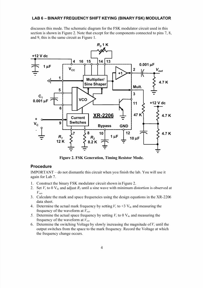
LAB 6 – BINARY FREQUENCY SHIFT KEYING (BINARY FSK) MODULATOR
discusses this mode. The schematic diagram for the FSK modulator circuit used in this
section is shown in Figure 2. Note that except for the components connected to pins 7, 8,and 9, this is the same circuit as Figure 1.
+1+1
VCOVCO
Current
Switches
VCC
GND
1
14
2
3
8
9
4
5
6
7 10 12
13
11
47 K
4.7 K
4.7 K
C1
0.001 µF +12 V dc
+12 V dc
1 µF
Mult.
0.001 µF
XR-2206
Multiplier/
Sine Shaper
Bypass
1516
V out
4.7 K
10 µFR 2
8.2 K
R 3
1 K
1 µF
+
VC
-
R 1
12 K
Figure 2. FSK Generation, Timing Resistor Mode.
Procedure
IMPORTANT – do not dismantle this circuit when you finish the lab. You will use it
again for Lab 7.
1. Construct the binary FSK modulator circuit shown in Figure 2.
2. Set V c to 0 Vdc and adjust R3 until a sine wave with minimum distortion is observed atV out .
3. Calculate the mark and space frequencies using the design equations in the XR-2206
data sheet.4. Determine the actual mark frequency by setting V c to +3 Vdc and measuring the
frequency of the waveform at V out .
5. Determine the actual space frequency by setting V c to 0 Vdc and measuring the
frequency of the waveform at V out .
6. Determine the switching Voltage by slowly increasing the magnitude of V c until the
output switches from the space to the mark frequency. Record the Voltage at which
the frequency change occurs.
4

7/30/2019 Lab6 FSK Modulator
http://slidepdf.com/reader/full/lab6-fsk-modulator 5/5
LAB 6 – BINARY FREQUENCY SHIFT KEYING (BINARY FSK) MODULATOR
7. Replace the power supply that provides V c with a function generator. Set the
amplitude of the function generator output to 3-V p-p, 10-kHz square wave and adjustits offset to 1.5 Vdc. This will produce a waveform that switches between 0 and +3 V.
8. Observe the FSK output waveform at V out . (Use the same method as in step 8 of the
circuit-1 procedure.)
9. Sketch the binary waveform observed at the function generator output and the FSK waveform observed at the modulator output (V out ).
10. Measure the mark and space frequencies, and calculate the modulation index usingthe same method as in step 11 of the circuit-1 procedure.
11. Describe the relationship between the two waveforms sketched in step 9.12. Adjust the signal-generator frequency to 5 kHz and then to 15 kHz, while keeping the
levels at 0 and 3 V. Describe what effect varying the signal-generator frequency has
on the FSK signal.
13. Adjust V c to a 10-kHz square wave switching between 0 and 2 V and then to a 10-
kHz, 4-V p-p square wave switching between 0 and 4 V. Does changing the amplitudeof the square wave affect the FSK signal?
6. Discussion Questions
1. In Figure 1, what determines the modulation index?
2. In Figure 2, what determines the modulation index?3. Considering your answers to questions 1 and 2, if the input were a digital signal,
which circuit would be better for an FSK modulator?
5


![Lab6-JdbcTemplate Trinh Bay[1]](https://static.fdocuments.in/doc/165x107/577cc2ae1a28aba711945c02/lab6-jdbctemplate-trinh-bay1.jpg)