Lab 18/D5: Analog Digital; PLL Contents - Harvard...
12
Chapter 18L Lab 18/D5: Analog ↔ Digital; PLL Contents 18LLab 18/D5: Analog ↔ Digital; PLL 1 18L.1Analog to Digital Converter (“ADC”) ............................................. 2 18L.1.1D/A Converter (“DAC”) ................................................ 2 18L.1.2ADC: Watching the Conversion Process ........................................ 3 18L.1.3Speed Limit ...................................................... 6 18L.1.4Completing the ADC: Latching the Digital Output ................................... 6 18L.2Phase-Locked Loop: Frequency Multiplier (We hope you’ll build this; but some people will not have time.) .......... 7 18L.2.1Generating a multiple of line frequency: (Type II detector) ............................... 8 18L.2.2Try FM demodulation (in slow motion) ........................................ 10 18L.2.3Expanded Lock Range: × 64 rather than × 1k ..................................... 11 REV 0 1 ; July 7, 2014. Contents This lab presents two devices, both partially digital, that have in common the use of feedback to generate an output related in a useful way to an input signal. The first circuit, an analog-to-digital converter (“ADC”), uses 1 Revisions: add headerfile and index (7/14); slightly-revise pll figure, spreading it out (3/12); fix pin mention for Q6, p. 11, add footnote saying that National’s pin numbering begins with Q1, strangely (2/12). 1
Transcript of Lab 18/D5: Analog Digital; PLL Contents - Harvard...
Chapter 18L
Lab 18/D5: Analog ↔ Digital; PLL
Contents
18LLab 18/D5: Analog ↔ Digital; PLL 118L.1Analog to Digital Converter (“ADC”) . . . . . . . . . . . . . . . . . . . . . . . . . . . . . . . . . . . . . . . . . . . . . 2
18L.1.1D/A Converter (“DAC”) . . . . . . . . . . . . . . . . . . . . . . . . . . . . . . . . . . . . . . . . . . . . . . . . 218L.1.2ADC: Watching the Conversion Process . . . . . . . . . . . . . . . . . . . . . . . . . . . . . . . . . . . . . . . . 318L.1.3Speed Limit . . . . . . . . . . . . . . . . . . . . . . . . . . . . . . . . . . . . . . . . . . . . . . . . . . . . . . 618L.1.4Completing the ADC: Latching the Digital Output . . . . . . . . . . . . . . . . . . . . . . . . . . . . . . . . . . . 6
18L.2Phase-Locked Loop: Frequency Multiplier (We hope you’ll build this; but some people will not have time.) . . . . . . . . . . 718L.2.1Generating a multiple of line frequency: (Type II detector) . . . . . . . . . . . . . . . . . . . . . . . . . . . . . . . 818L.2.2Try FM demodulation (in slow motion) . . . . . . . . . . . . . . . . . . . . . . . . . . . . . . . . . . . . . . . . 1018L.2.3Expanded Lock Range: × 64 rather than × 1k . . . . . . . . . . . . . . . . . . . . . . . . . . . . . . . . . . . . . 11
REV 01; July 7, 2014.
ContentsThis lab presents two devices, both partially digital, that have in common the use of feedback to generate anoutput related in a useful way to an input signal. The first circuit, an analog-to-digital converter (“ADC”), uses
1Revisions: add headerfile and index (7/14); slightly-revise pll figure, spreading it out (3/12); fix pin mention for Q6, p. 11, addfootnote saying that National’s pin numbering begins with Q1, strangely (2/12).
1
2 Lab 18/D5: Analog ↔ Digital; PLL
feedback to generate the digital equivalent to an analog input voltage. The second circuit, a phase-locked loop(“PLL”), uses feedback to generate a signal matched in frequency to the input signal—or to some multiple ofthat frequency.
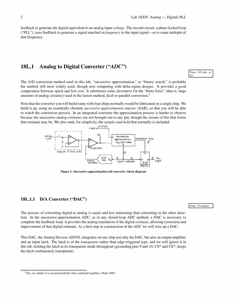
18L.1 Analog to Digital Converter (“ADC”)Time: 105 min., to-tal
The A/D conversion method used in this lab, “successive approximation,” or “binary search,” is probablythe method still most widely used, though now competing with delta-sigma designs. It provides a goodcompromise between speed and low cost. It substitutes some cleverness for the “brute force” (that is, largeamounts of analog circuitry) used in the fastest method, flash or parallel conversion.2
Note that the converter you will build today with four chips normally would be fabricated on a single chip. Webuild it up, using an essentially obsolete successive-approximation register (SAR), so that you will be ableto watch the conversion process. In an integrated converter the approximation process is harder to observebecause the successive analog estimates are not brought out to any pin, though the stream of bits that formsthat estimate may be. We also omit, for simplicity, the sample-and-hold that normally is included.
Figure 1: Successive-approximation a/d converter: block diagram
18L.1.1 D/A Converter (“DAC”)Time: 15 minutes
The process of converting digital to analog is easier and less interesting than converting in the other direc-tion. In the successive-approximation ADC, as in any closed-loop ADC method, a DAC is necessary tocomplete the feedback loop: it provides the analog translation of the digital estimate, allowing correction andimprovement of that digital estimate. As a first step in construction of the ADC we will wire up a DAC.
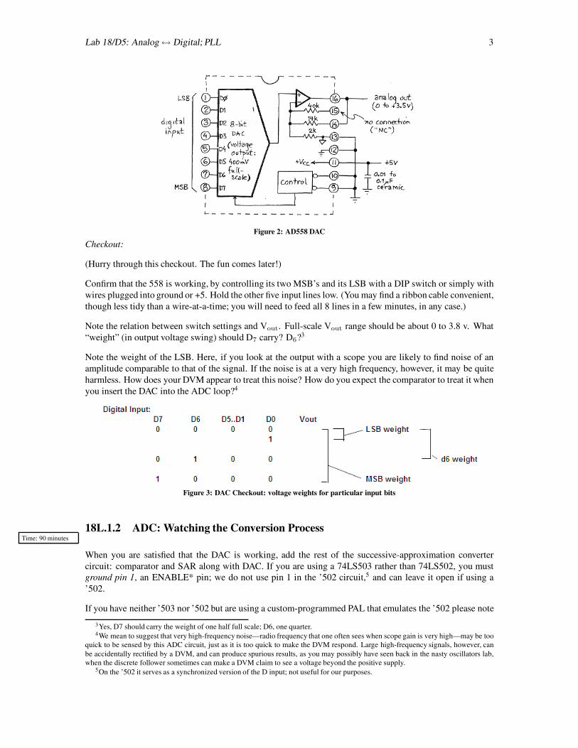
This DAC, the Analog Devices AD558, integrates on one chip not only the DAC, but also an output amplifierand an input latch. The latch is of the transparent rather than edge-triggered type, and we will ignore it inthis lab, holding the latch in its transparent mode throughout (grounding pins 9 and 10, CS* and CE*, keepsthe latch continuously transparent).
2Yes, we admit, it is an unusual brute who could put together a flash ADC.
Lab 18/D5: Analog ↔ Digital; PLL 3
Figure 2: AD558 DAC
Checkout:
(Hurry through this checkout. The fun comes later!)
Confirm that the 558 is working, by controlling its two MSB’s and its LSB with a DIP switch or simply withwires plugged into ground or +5. Hold the other five input lines low. (You may find a ribbon cable convenient,though less tidy than a wire-at-a-time; you will need to feed all 8 lines in a few minutes, in any case.)
Note the relation between switch settings and Vout. Full-scale Vout range should be about 0 to 3.8 v. What“weight” (in output voltage swing) should D7 carry? D6?3
Note the weight of the LSB. Here, if you look at the output with a scope you are likely to find noise of anamplitude comparable to that of the signal. If the noise is at a very high frequency, however, it may be quiteharmless. How does your DVM appear to treat this noise? How do you expect the comparator to treat it whenyou insert the DAC into the ADC loop?4
Figure 3: DAC Checkout: voltage weights for particular input bits
18L.1.2 ADC: Watching the Conversion ProcessTime: 90 minutes
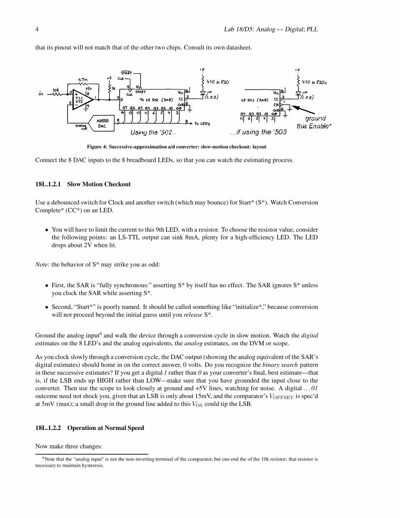
When you are satisfied that the DAC is working, add the rest of the successive-approximation convertercircuit: comparator and SAR along with DAC. If you are using a 74LS503 rather than 74LS502, you mustground pin 1, an ENABLE* pin; we do not use pin 1 in the ’502 circuit,5 and can leave it open if using a’502.
If you have neither ’503 nor ’502 but are using a custom-programmed PAL that emulates the ’502 please note
3Yes, D7 should carry the weight of one half full scale; D6, one quarter.4We mean to suggest that very high-frequency noise—radio frequency that one often sees when scope gain is very high—may be too
quick to be sensed by this ADC circuit, just as it is too quick to make the DVM respond. Large high-frequency signals, however, canbe accidentally rectified by a DVM, and can produce spurious results, as you may possibly have seen back in the nasty oscillators lab,when the discrete follower sometimes can make a DVM claim to see a voltage beyond the positive supply.
5On the ’502 it serves as a synchronized version of the D input; not useful for our purposes.
4 Lab 18/D5: Analog ↔ Digital; PLL
that its pinout will not match that of the other two chips. Consult its own datasheet.
Figure 4: Successive-approximation a/d converter: slow-motion checkout: layout
Connect the 8 DAC inputs to the 8 breadboard LEDs, so that you can watch the estimating process.
18L.1.2.1 Slow Motion Checkout
Use a debounced switch for Clock and another switch (which may bounce) for Start* (S*). Watch ConversionComplete* (CC*) on an LED.
• You will have to limit the current to this 9th LED, with a resistor. To choose the resistor value, considerthe following points: an LS-TTL output can sink 8mA, plenty for a high-efficiency LED. The LEDdrops about 2V when lit.
Note: the behavior of S* may strike you as odd:
• First, the SAR is “fully synchronous:” asserting S* by itself has no effect. The SAR ignores S* unlessyou clock the SAR while asserting S*.
• Second, “Start*” is poorly named. It should be called something like “initialize*,” because conversionwill not proceed beyond the initial guess until you release S*.
Ground the analog input6 and walk the device through a conversion cycle in slow motion. Watch the digitalestimates on the 8 LED’s and the analog equivalents, the analog estimates, on the DVM or scope.
As you clock slowly through a conversion cycle, the DAC output (showing the analog equivalent of the SAR’sdigital estimates) should home in on the correct answer, 0 volts. Do you recognize the binary search patternin these successive estimates? If you get a digital 1 rather than 0 as your converter’s final, best estimate—thatis, if the LSB ends up HIGH rather than LOW—make sure that you have grounded the input close to theconverter. Then use the scope to look closely at ground and +5V lines, watching for noise. A digital . . . 01outcome need not shock you, given that an LSB is only about 15mV, and the comparator’s VOFFSET is spec’dat 5mV (max); a small drop in the ground line added to this VOS could tip the LSB.
18L.1.2.2 Operation at Normal Speed
Now make three changes:
6Note that the “analog input” is not the non-inverting terminal of the comparator, but one end the of the 10k resistor; that resistor isnecessary to maintain hysteresis.
Lab 18/D5: Analog ↔ Digital; PLL 5
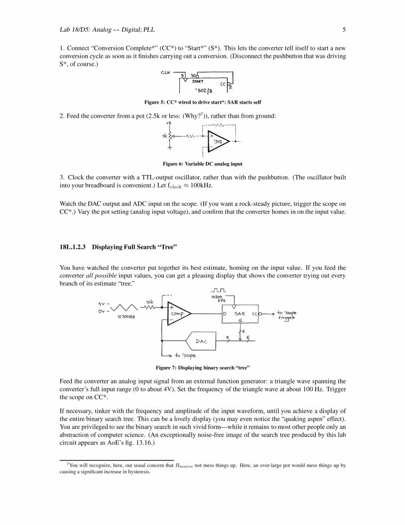
1. Connect “Conversion Complete*” (CC*) to “Start*” (S*). This lets the converter tell itself to start a newconversion cycle as soon as it finishes carrying out a conversion. (Disconnect the pushbutton that was drivingS*, of course.)
Figure 5: CC* wired to drive start*: SAR starts self
2. Feed the converter from a pot (2.5k or less: (Why?7)), rather than from ground:
Figure 6: Variable DC analog input
3. Clock the converter with a TTL-output oscillator, rather than with the pushbutton. (The oscillator builtinto your breadboard is convenient.) Let fclock ≈ 100kHz.
Watch the DAC output and ADC input on the scope. (If you want a rock-steady picture, trigger the scope onCC*.) Vary the pot setting (analog input voltage), and confirm that the converter homes in on the input value.
18L.1.2.3 Displaying Full Search “Tree”
You have watched the converter put together its best estimate, homing on the input value. If you feed theconverter all possible input values, you can get a pleasing display that shows the converter trying out everybranch of its estimate “tree.”
Figure 7: Displaying binary search “tree”
Feed the converter an analog input signal from an external function generator: a triangle wave spanning theconverter’s full input range (0 to about 4V). Set the frequency of the triangle wave at about 100 Hz. Triggerthe scope on CC*.
If necessary, tinker with the frequency and amplitude of the input waveform, until you achieve a display ofthe entire binary search tree. This can be a lovely display (you may even notice the “quaking aspen” effect).You are privileged to see the binary search in such vivid form—while it remains to most other people only anabstraction of computer science. (An exceptionally noise-free image of the search tree produced by this labcircuit appears as AoE’s fig. 13.16.)
7You will recognize, here, our usual concern that Rsource not mess things up. Here, an over-large pot would mess things up bycausing a significant increase in hysteresis.
6 Lab 18/D5: Analog ↔ Digital; PLL
18L.1.3 Speed Limit
The ADC completes an 8-bit conversion in nine clock cycles. Evidently, the faster you can clock it, the fasterit can convert. The faster it can convert, the higher the frequency of the input waveform that you can capture(you need a shade more than two samples per period, in theory; in practice you may want to take 3 to 5samples).
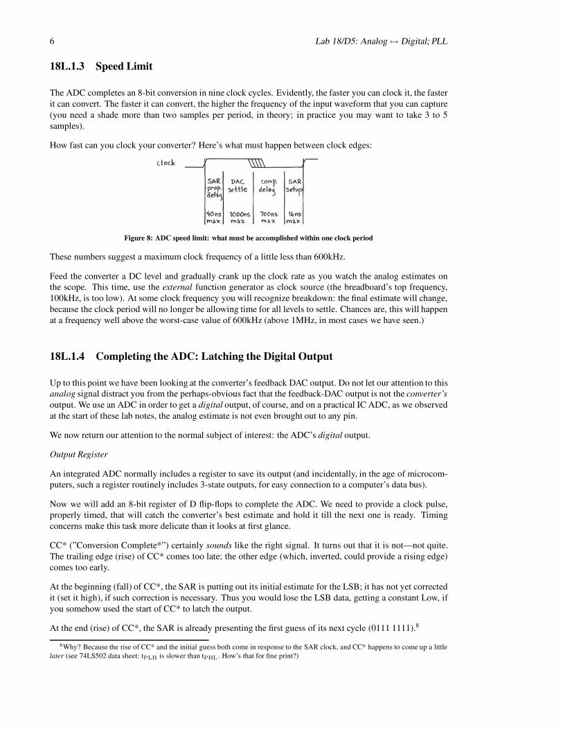
How fast can you clock your converter? Here’s what must happen between clock edges:
Figure 8: ADC speed limit: what must be accomplished within one clock period
These numbers suggest a maximum clock frequency of a little less than 600kHz.
Feed the converter a DC level and gradually crank up the clock rate as you watch the analog estimates onthe scope. This time, use the external function generator as clock source (the breadboard’s top frequency,100kHz, is too low). At some clock frequency you will recognize breakdown: the final estimate will change,because the clock period will no longer be allowing time for all levels to settle. Chances are, this will happenat a frequency well above the worst-case value of 600kHz (above 1MHz, in most cases we have seen.)
18L.1.4 Completing the ADC: Latching the Digital Output
Up to this point we have been looking at the converter’s feedback DAC output. Do not let our attention to thisanalog signal distract you from the perhaps-obvious fact that the feedback-DAC output is not the converter’soutput. We use an ADC in order to get a digital output, of course, and on a practical IC ADC, as we observedat the start of these lab notes, the analog estimate is not even brought out to any pin.
We now return our attention to the normal subject of interest: the ADC’s digital output.
Output Register
An integrated ADC normally includes a register to save its output (and incidentally, in the age of microcom-puters, such a register routinely includes 3-state outputs, for easy connection to a computer’s data bus).
Now we will add an 8-bit register of D flip-flops to complete the ADC. We need to provide a clock pulse,properly timed, that will catch the converter’s best estimate and hold it till the next one is ready. Timingconcerns make this task more delicate than it looks at first glance.
CC* (”Conversion Complete*”) certainly sounds like the right signal. It turns out that it is not—not quite.The trailing edge (rise) of CC* comes too late; the other edge (which, inverted, could provide a rising edge)comes too early.
At the beginning (fall) of CC*, the SAR is putting out its initial estimate for the LSB; it has not yet correctedit (set it high), if such correction is necessary. Thus you would lose the LSB data, getting a constant Low, ifyou somehow used the start of CC* to latch the output.
At the end (rise) of CC*, the SAR is already presenting the first guess of its next cycle (0111 1111).8
8Why? Because the rise of CC* and the initial guess both come in response to the SAR clock, and CC* happens to come up a littlelater (see 74LS502 data sheet: tPLH is slower than tPHL . How’s that for fine print?)
Lab 18/D5: Analog ↔ Digital; PLL 7
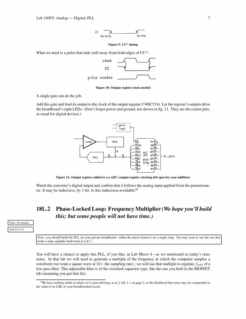
Figure 9: CC* timing
What we need is a pulse that ends well away from both edges of CC*:
Figure 10: Output register clock needed
A single gate can do the job.
Add this gate and feed its output to the clock of the output register (74HC574). Let the register’s outputs drivethe breadboard’s eight LEDs. (Don’t forget power and ground, not shown in fig. 11. They are the corner pins,as usual for digital devices.)
Figure 11: Output register added to s-a ADC (output-register clocking left open for your addition)
Watch the converter’s digital output and confirm that it follows the analog input applied from the potentiome-ter. It may be indecisive, by 1 bit. Is this indecision avoidable?9
18L.2 Phase-Locked Loop: Frequency Multiplier (We hope you’ll buildthis; but some people will not have time.)
Time: 45 minutes
AoE §13.3.4
Note: you should build the PLL on your private breadboard—either the micro board or on a single strip. You may want to use the one thatholds a mike amplifier built back in Lab 7.
You will have a chance to apply this PLL, if you like, in Lab Micro 4—as we mentioned in today’s classnotes. In that lab we will need to generate a multiple of the frequency at which the computer samples awaveform (we want a square wave at 32× the sampling rate) ; we will use that multiple to regulate f3dB of alow-pass filter. This adjustable filter is of the switched-capacitor type, like the one you built in the MOSFETlab (assuming you got that far).
9We have nothing subtle in mind; we’re just referring, as in § 18L.1.1 on page 2, to the likelihood that noise may be comparable tothe value of an LSB, in your breadboarded circuit.
8 Lab 18/D5: Analog ↔ Digital; PLL
Thus we will make the filter follow our sampling rate (so as to clear away the spurious high-frequencyelements in the DAC’s steppy output waveform). This future application for the PLL explains some elementsof its design: particularly, its frequency range, set to cover most of the range of sampling rates you’re likelyto adopt.
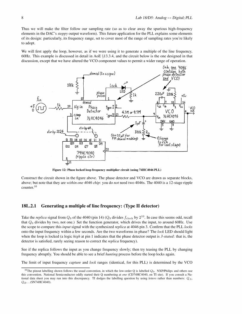
We will first apply the loop, however, as if we were using it to generate a multiple of the line frequency,60Hz. This example is discussed in detail in AoE §13.3.4, and the circuit below is the one designed in thatdiscussion, except that we have altered the VCO component values to permit a wider range of operation.
Figure 12: Phase locked loop frequency multiplier circuit (using 74HC4046 PLL)
Construct the circuit shown in the figure above. The phase detector and VCO are drawn as separate blocks,above; but note that they are within one 4046 chip: you do not need two 4046s. The 4040 is a 12-stage ripplecounter.10
18L.2.1 Generating a multiple of line frequency: (Type II detector)
Take the replica signal from Q9 of the 4040 (pin 14) (Q9 divides fclock by 210. In case this seems odd, recallthat Q0 divides by two, not one.) Set the function generator, which drives the input, to around 60Hz. Usethe scope to compare this input signal with the synthesized replica at 4046 pin 3. Confirm that the PLL locksonto the input frequency within a few seconds. Are the two waveforms in phase? The lock LED should lightwhen the loop is locked (a logic high at pin 1 indicates that the phase detector output is 3-stated: that is, thedetector is satisfied, rarely seeing reason to correct the replica frequency).
See if the replica follows the input as you change frequency slowly; then try teasing the PLL by changingfrequency abruptly. You should be able to see a brief hunting process before the loop locks again.
The limit of input frequency capture and lock ranges (identical, for this PLL) is determined by the VCO
10The pinout labelling shown follows the usual convention, in which the low-order Q is labelled Q0. NXP/Philips and others usethis convention. National Semiconductor oddly started their Q numbering at one (CD74HC4040, on TI site). If you consult a Na-tional data sheet you may run into this discrepancy. TI dodges the labelling question by using letters rather than numbers: QA,QB . . . (SN74HC4040).
Lab 18/D5: Analog ↔ Digital; PLL 9
range: from about 40kHz to 250kHz, for the specified values of R1, C1: 220k, 220pF. Since the counter inthe feedback path divides by 210, the input frequency range runs from approximately 40Hz to 250Hz.
18L.2.1.1 The Loop Filter
The hard part of PLL design comes in designing the low-pass filter to maintain stability. The PLL uses afeedback loop strikingly reminiscent of the loop in the PID motor-control lab: in the PID exercise, the motor-to-position transducer placed an integration inside the loop. This 90◦ lag obliged us to use care to avoidinjecting another 90-degree lag, at frequencies where loop gain was above unity.
In the PLL, again an integration lies within the loop, and again it threatens us with instability. This time,the integration results from the fact that we are sensing a characteristic (phase) that is an integral of thecharacteristic that our loop means to control (frequency). Here, the integration is harder to localize thanin the PID loop, where it clearly occurred in the motor-potentiometer unit. In the PLL the integration—the equivalent of the motor-pot combination—is performed by the VCO-phase-detector pair. The detector’soutput is a signal that measures phase error.11 For a constant frequency difference, the phase error (differencebetween input signal and the replica generated by the VCO) ramps; in other words, it integrates the frequencyerror. You will find a scope image that demonstrates this ramping effect in today’s class notes. This behaviorclosely resembles what we saw in the motor-pot combination: a constant error signal fed to the motor-potproduced a ramping output voltage: integration, once more.12
We need a low-pass filter in the loop, to smooth the signal into the VCO—but we cannot afford another 90◦
lag. What is to be done? The answer turns out to be a simple circuit amendment: use a low-pass whosephase shift at high frequencies goes toward zero rather than toward −90◦. A low-pass with an extra resistorbetween cap and ground does the trick, as today’s class notes argue.
If you replace the filter’s 330k resistor with 22k, you shouldfind that the loop hunts much longer—overshooting,backtracking. . . . Watching the demod signal, at pin 10, which shows the VCO input voltage, may make thehunting and overshooting vivid for you.
By reducing that R value, you have made a dangerous reduction in the phase margin—the safety marginbetween the phase shift around the loop (at the frequency where the loop gain goes to unity) and the edge ofthe cliff: the deadly −180◦ shift. This is a notion you will recall from Lab 9 (“. . .Nasty Oscillators”) andfrom the PID lab.
If you want to live really dangerously, short out the lower resistor; now you have reduced the phase margin tozero, and the circuit may hunt forever. When you have seen this effect, restore the 330k, to restore stability.
What frequency should be present at the VCO output when the loop is locked? Check your prediction bylooking with the scope at that point (pin 4 of the 4046). Why is this waveform jittery? (in a world withoutnoise it would not be.)13
Now look at the output of the phase detector (pin 13 of the 4046). This is the type II detector described inCh. 9 (sec. 9.27, pp. 644-45). You’ll notice a string of brief positive going pulses, each decaying away
11You may be inclined to ask, “Why do this? Why not be more straightforward and measure frequency error directly?” The answeris that we have no way to do that quickly. To measure frequency even indirectly, inferring it from period, requires waiting for a fullperiod of the two waveforms. Phase error information is available more promptly: after each of the respective rising edges, in the TypeII detector.
12If you’re not exhausted by this discussion, you may want to consider a complication: a second integration performed by the RC,at least as used in the edge-sensitive “Type II” detector: a constant phase difference produces a ramping output from the phase detector.This second integration is analogous to the I used in the PID circuit. The I term drives the PID error to zero; the Type II detector,similarly, uses this integration to drive the phase difference to zero.
13The jitter arises because the corrections to VCO frequency come only once in every 1024 cycles of the VCO output. Slightwanderings of frequency, between these checks, go uncorrected. As usual, being college teachers, we are reminded of the fact—probably beneficial to humans, though unsettling in the PLL analogy—that the college checks whether students can do the course workonly now and then: at best, weekly; the big test comes only once per term. In the meantime, who knows what goes on in the student’slife? No doubt that life would be full of jitter, if one were so rude as to look at it between checkpoints.
10 Lab 18/D5: Analog ↔ Digital; PLL
exponentially when the detector reverts to its 3-stated condition (you may also see smaller negative-goingpulses, to the extent that the circuit is troubled by noise).
Theory predicts that these correction pulses should vanish in the steady state. But the 10 megohm load of thescope probe you are using is discharging the filter capacitor fast enough to cause the pulses; the current thescope draws also causes the VCO to be slightly under-driven, causing the VCO to run a little late; a laggingphase difference persists: the loop now needs a phase difference, so as to provide the positive pulses that feedthe scope’s R to ground. If you’re feeling energetic, interpose a 358 op amp follower between the capacitorand the probe. The positive pulses should become narrower—and now the phase difference is reversed: theVCO output comes a little early.14
18L.2.2 Try FM demodulation (in slow motion)
If you watch the input to the VCO (which is available in buffered form at pin 10), you can see a measure ofVCO frequency. That’s not very interesting when the input frequency is constant—but becomes interestingwhen a variation in input frequency carries information, as it does in an FM radio broadcast (or in our analogproject, where we sent music across the room with an LED’s flashes). We aren’t going to pause long enoughto do such an exercise, here; but we suggest that you get a glimpse of the way it might work, with a two-minutedemonstration.
Replace the 1μF capacitor, temporarily, with a 0.1μF part (to make the loop adjust faster), and watch thedemod signal (pin 10) as you try to vary fIN sinusoidally, by slowly varying the function generator frequency.You should sweep the scope very slowly—using “roll” mode (perhaps 1s/div) if you have a digital scope. Wehope the demod signal will look like the sinusoid that varies or “modulates” the PLL’s input frequency. Toobad we didn’t know about PLL’s when we did the group audio-LED project.
When you’ve had enough fun with this, restore the 1μF capacitor.
Type I Detector (exclusive-OR)
The 74HC4046 includes three phase detectors. AoE describes two of them (types I and II) in §13.3.2.1.15 Thethird detector on the HC4046, Type III, is simply a variation on the SR latch, with S and R driven by positivelevels on the input and replica lines, respectively. We will ignore the Type III detector:16 two detectors seemplenty to consider on a first encounter with a PLL. But feel free to check out the Type III, if you like: itsoutput appears at pin 15.
The Type I detector output is at pin 2, and the inputs are the same as for the type II detector; to use the TypeI, simply move the wire from pin 13 to pin 2 (and then to 15 for the Type III, if you must!). For both TypeI and Type III you should be able to see the fluctuation of the VCO frequency over the period of the input,which you can exaggerate by reducing the size of the 1μF loop filter capacitor.
If you make a sudden, large change in the input frequency, you should be able to fool the type I circuit intolocking onto a harmonic of the input frequency (a multiple of the input frequency). For our purpose in LabMicro 4, such an error would make the circuit useless, so we will use the Type II detector. You are likely tomake the same choice in most applications.
Note also the phase difference that persists between input and feedback signal in the locked state. This simplephase detector (like the Type III) requires such a phase difference; this difference generates the signal thatdrives the VCO. If the phase difference ever goes to zero (or to π), the loop loses feedback: it can no longercorrect frequency in both senses, as required. When it hits that limit, it’s like an op amp feedback loop
14Why? It’s a fussy detail, but now, instead of discharging, as the scope probe did, the ’358’s IBIAS injects some current from itsPNP input transistor’s base.
15AoE’s discussion treats the similar CD4046 rather than the 74HC version.16The type III detector was added as a sort of afterthought; early versions of the 4046 did not offer it. Like the simple XOR (Type I)
it requires a phase difference between input and replica signal.
Lab 18/D5: Analog ↔ Digital; PLL 11
that fails because the op amp output hits saturation and thus cannot make a further correction. The Type IIdetector is altogether classier: it requires no errors to keep the loop locked; it is able to use the capacitor as asample-and-hold, once the loop is locked, rather than as a conventional filter.
When you have finished looking at the behavior (and misbehavior) of the Type I detector, revert to the earliercircuit, using the Type II (output at pin 13).
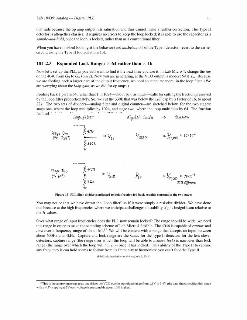
18L.2.3 Expanded Lock Range: × 64 rather than × 1k
Now let’s set up the PLL as you will want to find it the next time you use it, in Lab Micro 4: change the tapon the 4040 from Q9 to Q5 (pin 2). Now you are generating, at the VCO output, a modest 64 X fin . Becausewe are feeding back a larger part of the output frequency, we need to attenuate more, in the loop filter. (Weare worrying about the loop gain, as we did for op amps.)
Feeding back 1 part in 64, rather than 1 in 1024—about 16× as much—calls for cutting the fraction preservedby the loop filter proportionately. So, we cut the 330k that was below the 1μF cap by a factor of 16, to about22k. The two sets of dividers—analog filter and digital counter—are sketched below, for the two stages:stage one, where the loop multiplies by 1024, and stage two, where the loop multiplies by 64. The fractionfed back is held roughly constant (to about 12%) in the two cases.
Figure 13: PLL filter divider is adjusted to hold fraction fed back roughly constant in the two stages
You may notice that we have drawn the “loop filter” as if it were simply a resistive divider. We have donethat because at the high frequencies where we anticipate challenges to stability XC is insignificant relative tothe R values.
Over what range of input frequencies does the PLL now remain locked? The range should be wide; we needthis range in order to make the sampling scheme of Lab Micro 4 flexible. The 4046 is capable of capture andlock over a frequency range of about 6:1.17 We will be content with a range that accepts an input betweenabout 600Hz and 4kHz. Capture and lock range are the same, for the Type II detector; for the less cleverdetectors, capture range (the range over which the loop will be able to achieve lock) is narrower than lockrange (the range over which the loop will hang on once it has locked). This ability of the Type II to captureany frequency it can hold seems to follow from its immunity to harmonics: you can’t fool the Type II.
(labd5 adc headerfile july14.tex; July 7, 2014)
17This is the approximate range as one drives the VCO over its permitted range from 1.1V to 3.4V (the data sheet specifies this rangewith a 4.5V supply; at 5V each voltage is presumably about 10% higher).
Index
74HC4040 (lab), 874HC4046 (lab), 874HC574 (lab), 674LS503 (lab), 3
AD558 (lab), 2ADC (lab), 3–7
binary search (lab), 2binary search display (lab), 5
CC* (lab), 4
DAC (lab), 2–3
FM demodulationPLL (lab), 10
phase-locked loopFM demodulation (lab), 10loop filter (lab), 9phase detector
XOR (lab), 10phase-locked loop (lab), 7–11
SAR (lab), 2
12