L16: Power Dissipation in Digital Systems · PDF fileL16: Power Dissipation in Digital...
23
L16: 6.111 Spring 2006 1 Introductory Digital Systems Laboratory L16: Power Dissipation in Digital Systems L16: Power Dissipation in Digital Systems
Transcript of L16: Power Dissipation in Digital Systems · PDF fileL16: Power Dissipation in Digital...

L16: 6.111 Spring 2006 1Introductory Digital Systems Laboratory
L16: Power Dissipation in Digital SystemsL16: Power Dissipation in Digital Systems

L16: 6.111 Spring 2006 2Introductory Digital Systems Laboratory
Problem #1: Power Dissipation/HeatProblem #1: Power Dissipation/Heat
5KW 18KW
1.5KW 500W
40048008
80808085
8086286
386486
Pentium® proc
0.1
1
10
100
1000
10000
100000
1971 1974 1978 1985 1992 2000 2004 2008Year
Pow
er (W
atts
)
400480088080
8085
8086
286 386486
Pentium® procP6
1
10
100
1000
10000
1970 1980 1990 2000 2010Year
Pow
er D
ensi
ty (W
/cm
2)
Hot Plate
NuclearReactor
RocketNozzle
Sun’sSurface
Courtesy Intel (S. Borkar)
How do you cool these chips??How do you cool these chips??
chip
heat sink

L16: 6.111 Spring 2006 2Introductory Digital Systems Laboratory
Problem #2: Energy ConsumptionProblem #2: Energy Consumption
(Image by MIT OCW. Adapted from Jon Eager, Gates Inc. , S. Watanabe, Sony Inc.)
No Moore’s law for batteries…Today: Understand where power goes
and ways to manage it
What can One Jouleof energy do?
Send a 1 Megabyte file over 802.11b
Operate a processor
for ~ 7s
The Energy Problem
7.5 cm3
AA battery
Alkaline: ~10,000J
Mow your lawn for
1 ms
Image by MIT OCW.

L16: 6.111 Spring 2006 3Introductory Digital Systems Laboratory
Dynamic Energy DissipationDynamic Energy Dissipation
VDD
CL
E0→1 = CLVDD2
Ecap = 1/2CLVDD2iDD
Ediss, RP = 1/2CLVDD2
VDD
CL
IN =1Ediss,RN =1/2CLVDD
2
Charging Discharging
IN =0
P = CL VDD2 fclk
RN
RP
RN
RP

L16: 6.111 Spring 2006 4Introductory Digital Systems Laboratory
The Transition Activity Factor The Transition Activity Factor αα00−−>>11
Current Next Output Input Input Transition
00 00 1 −> 100 01 1 −> 100 10 1 −> 100 11 1 −> 001 00 1 −> 101 01 1 −> 101 10 1 −> 101 11 1 −> 010 00 1 −> 110 01 1 −> 110 10 1 −> 110 11 1 −> 011 00 0 −> 111 01 0 −> 111 10 0 −> 111 11 0 −> 0
α0−>1 = 3/16
Assume inputs (A,B) arrive at f and are uniformly distributedWhat is the average power dissipation?
P = α0−>1 CL VDD2 f
ZAB

L16: 6.111 Spring 2006 5Introductory Digital Systems Laboratory
Junction (Silicon) TemperatureJunction (Silicon) Temperature
Simple Scenario
Tj-Ta= RθJA PD
Silicon
RθJA is the thermal resistance between silicon and Ambient
RθJAPD
Tj= Ta + RθJA PD
Make this as low as possible
Realistic Scenario
RθJCPD
RθCA = RθCS + RθSA
SinkCase
Silicon
TJ
TA
TJ
TC
TS
TATJ
TC
TS
TA
RθCS
RθSA
is minimized by facilitating heat transfer (bolt case to extended metal surface – heat sink)

L16: 6.111 Spring 2006 6Introductory Digital Systems Laboratory
Intel Pentium 4 Thermal GuidelinesIntel Pentium 4 Thermal Guidelines
Pentium 4 @ 3.06 GHz dissipates 81.8W!Maximum TC = 69 °CRCA < 0.23 °C/W for 50 C ambientTypical chips dissipate 0.5-1W (cheap packages without forced air cooling)
Image by MIT OpenCourseWare. Image by MIT OpenCourseWare. Adapted from Intel Pentium 4 documentation.
.

L16: 6.111 Spring 2006 7Introductory Digital Systems Laboratory
Power Reduction StrategiesPower Reduction Strategies
Reduce Transition Activity or Switching EventsReduce Capacitance (e.g., keep wires
short)Reduce Power Supply VoltageFrequency is typically fixed by the application, though this can be adjusted to control power
P = α0−>1 CL VDD2 f
Optimize at all levels of design hierarchyOptimize at all levels of design hierarchy

L16: 6.111 Spring 2006 8Introductory Digital Systems Laboratory
Clock Gating is a Good Idea!Clock Gating is a Good Idea!
+
X
Global Clock Adder Clock
Multiplier Clock
Adder Off
Enable_Adder
Enable_Multiplier
Multiplier On
100’s of different clocks in a microprocessor
Clock Gating Reduces Energy, does it reduce Power?Clock Gating Reduces Energy, does it reduce Power?
Clock gating reduces activityand is the most common low-power
technique used today

L16: 6.111 Spring 2006 9Introductory Digital Systems Laboratory
Does your GHz Processor run at a GHz? Does your GHz Processor run at a GHz?
Processor
ThermalSensor
Note that there is a difference between average and peak power
On-chip thermal sensor (diode based), measures the silicon temperature
If the silicon junction gets too hot (say 125 °C), then the activity is reduced (e.g., reduce clock rate or use clock gating)
ChipActivity Control
Use of Thermal FeedbackUse of Thermal Feedback

L16: 6.111 Spring 2006 10Introductory Digital Systems Laboratory
Power Supply ResonancePower Supply Resonance
Lboard Lpackage Rgrid
Switchingcurrents
Board decap
On-diedecap
Can write a Virus to Activate Can write a Virus to Activate
Power Supply Resonance!Power Supply Resonance!
Image removed due to copyright restrictions.
Image removed due to copyright restrictions.
Image removed due to copyright restrictions.

L16: 6.111 Spring 2006 11Introductory Digital Systems Laboratory
Number Representation:Number Representation:TwoTwo’’s Complement vs. Sign Magnitudes Complement vs. Sign Magnitude
Sign-MagnitudeTwo’s complement
Consider a 16 bit bus where inputs togglesbetween +1 and –1 (i.e., a small noise input)Which representation is more energy efficient?
0000
0111
0011
1011
11111110
1101
1100
1010
1001
1000
0110
0101
0100
0010
0001
+0+1
+2
+3
+4
+5
+6
+7-0
-1
-2
-3
-4
-5
-6
-7

L16: 6.111 Spring 2006 12Introductory Digital Systems Laboratory
Time Sharing is a Bad IdeaTime Sharing is a Bad Idea
Time Sharing Increases Switching ActivityTime Sharing Increases Switching Activity
2

L16: 6.111 Spring 2006 13Introductory Digital Systems Laboratory
Not just a 6Not just a 6--1 Issue: 1 Issue: ““CoolCool”” Software ???Software ???
CPU
0111111100000000
0111111100000001
0111111100000010
0111111100000011
1000000000000000
1000000000000001
1000000000000010
1000000000000011
a[0]a[1]a[2]a[3]
b[0]b[1]b[2]b[3]
float a [256], b[256];float pi= 3.14;
for (i = 0; i < 255; i++) {a[i] = sin(pi * i /256);}for (i = 0; i < 255; i++) {b[i] = cos(pi * i /256);}
float a [256], b[256];float pi= 3.14;
for (i = 0; i < 255; i++) {a[i] = sin(pi * i /256);b[i] = cos(pi * i /256);
}
address
MEMORY address
16
512(8)+2+4+8+16+32+64+128+256= 4607 bit transitions
2(8)+2(2+4+8+16+32+64+128+256)= 1030 transitions

L16: 6.111 Spring 2006 14Introductory Digital Systems Laboratory
GlitchingGlitching TransitionsTransitions
Balancing paths reduces glitching transitionsStructures such as multipliers have lot of glitching transitionsKeeping logic depths short (e.g., pipelining) reduces glitching
++
+
A B C D
(A+B) + (C+D)+
+
+
A B
C
D
(((A+B) + C)+D)
Chain Topology Tree Topology
L16: 6.111 Spring 2006 15Introductory Digital Systems Laboratory
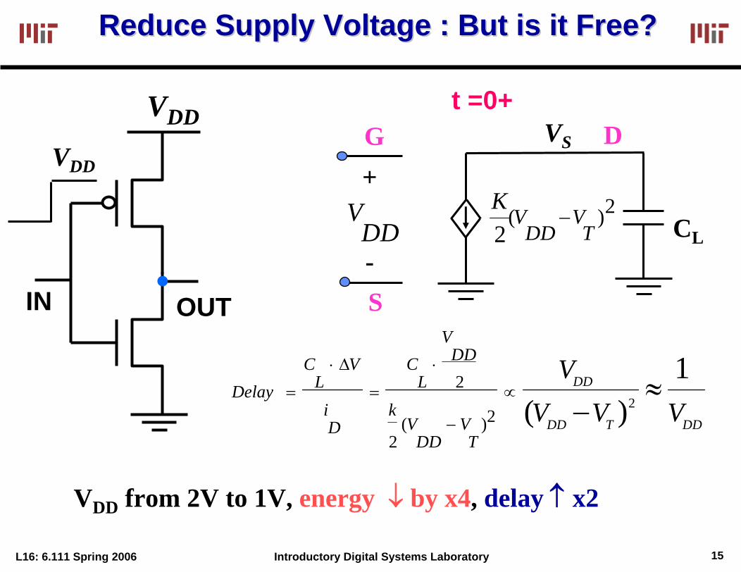
Reduce Supply Voltage : But is it Free?Reduce Supply Voltage : But is it Free?
IN OUT
VDD
+
-CL
t =0+
2)(2 T
VDD
VK
−
S
DDV
VDD
VSG D
DDTDD
DD
VVVV
TV
DDV
k
DDV
LC
Di
VL
CDelay
1)( 2
2)(2
2 ≈−
∝
−
⋅
=
Δ⋅
=
VDD from 2V to 1V, energy ↓ by x4, delay ↑ x2

L16: 6.111 Spring 2006 16Introductory Digital Systems Laboratory
Transistors Are FreeTransistors Are Free……(What do you do with a Billion Transistors?)(What do you do with a Billion Transistors?)
OUT
IN
X
Pserial = Cmult 22 f P
f =1GHzVDD=2V
parallel = (2Cmult 12 f /2) = Pserial/4
X X
INf = 500MhzVDD=1V
f = 500MhzVDD=1V
IN
SELECT
Trade Area for Low PowerTrade Area for Low Power
OUT

L16: 6.111 Spring 2006 17Introductory Digital Systems Laboratory
Algorithmic WorkloadAlgorithmic Workload
Exploit Time Varying Algorithmic WorkloadExploit Time Varying Algorithmic WorkloadTo Vary the Power Supply Voltage To Vary the Power Supply Voltage
Image by MIT OCW.
L16: 6.111 Spring 2006 18Introductory Digital Systems Laboratory
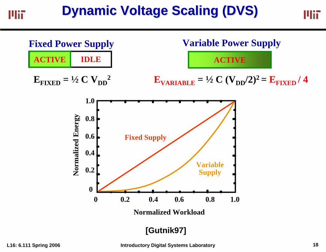
Dynamic Voltage Scaling (DVS)Dynamic Voltage Scaling (DVS)
ACTIVE IDLE
EFIXED = ½ C VDD2
Fixed Power SupplyACTIVE
EVARIABLE = ½ C (VDD/2)2 = EFIXED / 4
Variable Power Supply
0.2 0.4 0.8 1.0
0.2
0.4
0.6
0.8
1.0
Normalized Workload
Nor
mal
ized
Ene
rgy
Fixed Supply
VariableSupply
00 0.6
[Gutnik97]

L16: 6.111 Spring 2006 19Introductory Digital Systems Laboratory
DVS on a ProcessorDVS on a Processor
Digitally adjustable DC-DC converter powers SA-1110 core
μOS selects appropriate clock frequency based on workload and latency constraints
SA-1110
Control
μOS
VoutController
3.6V
5
Figure by MIT OpenCourseWare. Adaptedfrom R. Min, T. Furrer, and A. P. Chandrakasan."Dynamic Voltage Scaling Techniques forDistributed Microsensor Networks." Workshopon VLSI (April 2000): 43-46.
Ener
gy p
er O
pera
tion
Frequency (MHz) Core Voltage (V)
59.088.5
118.0147.5
176.9206.4
0.91.0
1.11.2
1.31.4
1.51.6
1
0.8
0.6
0.4
0.2
0

L16: 6.111 Spring 2006 20Introductory Digital Systems Laboratory
Energy Efficiency of SoftwareEnergy Efficiency of Software
CLB CLB
CLBCLB
FPGA (Xilinx)
““SoftwareSoftware”” Energy Dissipation has Large OverheadEnergy Dissipation has Large Overhead
Processor (StrongARM-1100)
0.25
0.2
0.15
0.1
0.05
0ARM Instructions
Aver
age
Cur
rent
(A)
Figure by MIT OpenCourseWare. Adapted from A. Sinha, DAC.
45
4035
30
2520
15
10
5
0Cache Cpntrol GCLK EBOX I/O,PLL
Pow
er (%
)
Figure by MIT OpenCourseWare. Adapted from Montanaro 1996, JSSC.
InterconnectClock
CLBI/O
5%9%
21%
65%
Image by MIT OpenCourseWare. Adapted from Kusse 1998, UCB.

L16: 6.111 Spring 2006 21Introductory Digital Systems Laboratory
Trends: Leakage and Power GatingTrends: Leakage and Power Gating
Low VTdevices are
leaky - Use a High VT
device is used to gate leakage current
Sleep
Duty Cycle (%)
Tota
l Ene
rgy/
Switc
hing
Ene
rgy
VDD
C
VDD
C
EE = = VVDDDDII001010--VVTT//SS
EE = = CVCVDDDD22
SwitchingSwitching(computing)(computing)
LeakageLeakage(standby)(standby)
0 1

L16: 6.111 Spring 2006 22Introductory Digital Systems Laboratory
Trends: Energy ScavengingTrends: Energy Scavenging
Image removed due to copyright restrictions.
Vibration-to-Electric Conversion
~ 10μW
MEMS Generator Power Harvesting Shoes
Courtesy of Joe Paradiso (MIT Media Lab). Used with permission.
After 3-6 steps, it provides 3 mAfor 0.5 sec
~10mW


![L16: Power Dissipation in Digital Systemsweb.mit.edu/6.111/www/s2006/LECTURES/l16.pdf · [Montanaro, JSSC ‘96] [A. Sinha, DAC] 65% 21% 9% 5% Interconnect Clock I/O CLB CLB CLB CLB](https://static.fdocuments.in/doc/165x107/6075f07be9a488213651b8cd/l16-power-dissipation-in-digital-montanaro-jssc-a96-a-sinha-dac-65-21.jpg)