KT11-C memory management unit maintenance manualbitsavers.informatik.uni-stuttgart.de/ · tives and...
90
KT11-C memory management unit maintenance manual
Transcript of KT11-C memory management unit maintenance manualbitsavers.informatik.uni-stuttgart.de/ · tives and...

KT11-C memory management unit maintenance manual


(
c
KT11-Cmemory manag'ement unit maintenance manual
DEC~ Il-HKTB-D
digital equipment corporation • maynard, massachusetts
1st Edition, April1972 2nd Printing (Rev) July 1972 3rd Printing, November 1972 4th Printing, February 1973 5th Printing, July 1973
Copyright © ·1972, 1973 by Digital Equipment Corporation
The material in this manual is for informational purposes and is subject to change without notice.
The following are trademarks of Digital Equipment Corporation, Maynard, Massachusetts:
DEC FLlPCIDP DIGITAL UNIBUS
PDP FOCAL COMPUTER LAB
(

( CONTENTS
Page
CHAPTER 1 GENERAL DESCRIPTION
1.1 Purpose of Option 1-1
1.2 Prerequisite 1-1
1.3 Features 1-1
1.3.1 Memory Protection 1-1
1.3.2 Re1ocation/Virtual Memory 1-3
1.3.3 Memory Expansion 1-3
1.3.4 Variable Size Pages 1-3
1.3.5 Page State Information 1-3
1.3.6 Instruction/Data Spaces 1-4
1.3.7 Kernel/Supervisor/User Spaces 1-4
1.3.8 Program vs Stack Pages 1-4
1.3.9 Fault Recovery 1-4
1.3.10 Statistical Traps 1-4
1.4 KT 11-C Memory Management Unit Specifications 1-4
CHAPTER 2 OPERATION AND PROGRAMMING
2.1 Basic KT11-C Mechanisms 2-1
2.1.1 Address Relocation Mechanism 2-1
C ! 2.1.2 Memory Protection Mechanisms 2-4
2.1.2.1 Non-Resident/Read-Only Protection 2-4 \ 2.1.2.2 Execute-Only Protection 2-4
2.1.2.3 Multiple Address Space Protection 2-5
2.1.3 Memory Management Statistics Mechanism 2-5
2.1.4 Trap/Abort Mechanism 2-6
2.2 PAR/PDR Registers 2-6
2.2.1 Page Address Registers (PAR) 2-7
2.2.2 Page Descriptor Registers (PDR) 2-8
2.2.2.1 Access Control Field (ACF) 2-9
2.2.2.2 Expansion Direction (ED) 2-9
2.2.2.3 Written Into (W) 2-10
2.2.2.4 Attention (A) 2-12
2.2.2.5 Page Length Field (PLF) 2-12
2.3 Memory Management Status Registers 2-13
2.3.1 Status Register 0 (SRO) 2-14
2.3.1.1 Abort-Nonresident 2-14
2.3.1.2 Abort-Page Length 2-14
2.3.1.3 Abort-Read Only 2-14
2.3.1.4 Trap-Memory Management 2-14
2.3.1.5 Bit 11 2-14
2.3.1.6 Enable Memory Management 2-15
2.3.1.7 Maintenance/Destination Mode 2-15
(~- 2.3.1.8 Instruction Completed 2-15
iii

CONTENTS (Cont) ( Page
2.3.1.9 Abort Recovery Information 2-15
2.3.1.10 Enable KT 11-C 2-15
2.3.2 Status Register 1 (SR 1) 2-15
2.3.3 Status Register 2 (SR2) 2-16
2.3.4 Status Register 3 (SR3) 2-17
2.4 KTl1-C Operation 2-17
2.4.1 Console Operations 2-17
2.4.1.1 Single Step Mode .2-17
2.4.1.2 Address Display 2-17
2.4.1.3 Stepping Over 32K-Word Boundaries 2-17
2.4.2 Physical Address Determination 2-17
2.4.3 Protection Without Relocation 2-18
2.4.4 Communication Between User/SuperVisor/Kernel Address 2-19
Space
2.4.4.1 Overlapping Physical Addresses 2-19
2.4.4.2 MFPI and MTPDInstructionsUse 2-19
2.4.4.3 Control Information 2-20
2.4.5 Statistical Aids Use 2-20
2.4.6 I and D Space Use 2-21
2.4.7 I/O Operations 2-22
2.4.7.1 Kernel Mode Protection 2-22 ( 2.4.7.2 Avoiding I/O Lockout 2-22
2.4.8 Processor Status Word 2~22
2.4.8.1 Explicit References to PS 2-22
2.4.8.2 Implicit Modification of the PS 2-23
2.4.9 Non-Recoverable Aborts 2-23
2.4.10 Page Fault Recovery 2-23
2.4.10.1 Definitions 2-23
2.4.10.2 Program Example 2-25
2.4.11 Fatal System Errors 2-28
CHAPTER 3 LOGIC DESCRIPTION .'
3.1 fDP-ll/45 System Interface 3-1
3.2 KTll-C Organization 3-2
3.2.1 System Address Path (SAP) 3-2
3.2.2 Status and Control Logic 3-2
3.3 PAR/PDR Registers ' 3-2
3.3.1 Page Address Registers (PAR) 3-4
3.3.1.1 Selection 3-4
3.3.1.2 Addressing 3-4
3.3.1.3 Writing Into a PAR 3-5
3.3.1.4 Reading From a PAR 3-5
3.3 . .2 Page Descriptor Registers (PDR) 3-5 l 3.3.2.1 Selection 3-5
iv
-. -----:;
( CONTENTS (Cont)
Page
3.3.2.2 Addressing 3-5 3.3.2.3 Writing Into a PDR 3-6 3.3.2.4 Setting A or W Bits 3-6 3.3.2.5 Clearing A or W Bits 3-6 3.3.2.6 Reading From a PDR 3-6 3.4 Relocation Logic 3-6 3.4.1 Address Inverters/Buffers 3-6 3.4.2 12-Bit Adder 3-6 3.4.3 Relocation Multiplexer 3-7 3.5 Co~sole Address Display and Control 3-7 3.5.1 ADDRESS Display 3-7 3.5.2 Console Mode Control 3-7 3.6 Abort and Trap Decode 3-7 3.6.1 Abort Control Logic 3-9 3.6.1.1 Non-Resident (NR) Page Fault 3-9 3.6.1.2 Resident Read-Only (RRO) Fault 3-9 3.6.1.3 Page Length Fault 3-9 3.6.2 Internal Register Inhibit 3-9 3.6.3 Memory Management Trap Decode 3-10 3.7 PAR/PDR Read Multiplexers 3-10
C' 3.8 Unibus Address Drivers 3-10 3.9 Status Register 3 (SR3) 3-10 3.10 KTlI-C ROM and Decode 3-10 3.10.1 ROM Organization 3-11 3.10.2 ROM OUT (4: 0 Decoders 3-12 3.10.2.1 RESTOREPS 3-13 3.10.2.2 SSRA JSR.30 (ROM (3: 0 = 5) 3-13 3.10.2.3 BRK.30 (ROM (3: 0 = 4) 3-13 3.10.2.4 AUTO DEC (ROM (3: 0 = 3) 3-13 3.10.2.5 ONE CHANGED (ROM (3:0=2 or 3) 3-13 3.10.2.6 DST 3-14 3.10.3 Kernel Space Control 3-14 3.10.4 Supervisor Space Control 3-14 3.10.5 User Space Control 3-14 3.10.6 I Space Control 3-14 3.11 Status Register 0 (SRO) 3-15 3.11.1 Abort Flags SRO <IS: 13) 3-15 3.11.2 Memory Management Trap (SRO Bit 12) 3-16 3.11.2.1 Enable Management Traps 3-16 n1.2.2 Pre-Management Trap 3-16 3.11.2.3 Memory Management Hold 3-16 3.11.2.4 Writing Into SRO Bit 12 3-19 3.11.3 Trap Flag (SRO Bit 11) 3-19
l \
3.11.4 DST MODE (SRO Bit 08) 3-19
v
3.11.5
3.11.6
3.11.7
3.11.8
3.11.9
3.12
3.12.1
3.12.2
3.12.3
3.13
3.14
3.15
3.15.1
3:15.2
3.15.3 . 3.16
3.16.1
3.16.2
3.16.2.1
3.16.2.2
3;16.3
CHAPTER 4
4.1
4.2
4.2.1
4.2.2
4.2.3
APPENDIX A
APPENDIXB
Figure No.
1-1
2-1
2-2
2-3
CONTENTS (Cont)
INSTR COMP (SRO Bit 07)
SRO Mode Field (SRO Bits (06:05»
Address Space - I/D (SRO Bit 04)
Page Number (SRO Bits (03:01»
KT 11-C Relocating (SWO Bit 00)
Status Register 1 (SR 1)
General Register Address
Autoincrement/ Autodecrement
Examples of SRI Loading
Status Register 2 (SR2)
Internal Data Bus Multiplexers
KT11-C Memory Management Timing
Event Times Related to Memory Cycles
Address Relocation Timing
Internal Register Access Timing
Internal Register Control
PAR/PDR Decode and Control
SSR Decode and Control
SSRREG
INTSR3
Internal Register Fast Decode
INSTALLATION AND MAINTENANCE
Installation
Maintenance
Diagnostic Programs
Troubleshooting Test Procedures
Repair Procedures
GLOSSARY
REFERENCE LITERATURE
ILLUSTRATIONS
Title
System Block Diagram
Basic KT11-C Relocation Mechanism
Relocation of a 32K-Word Program into, 124K-Word Physical
Memory
Construction of an 18-Bit Physical Address
vi
Page
3-19
3-19
3-20
3-20
3-20
3-20
3-20
3-21
3-21
3-22
3-22
3-23
3-23
3-23
3-23
3-23
3~28
3"28 3-28
3-28
3-28
4-1
4-1
4-1
4-1
4-1
A-I
B-1
Page
1-2
2-2
2-3
2-3
(
C

( ILLUSTRATIONS (Cont)
Figure No. Title Page
2-4 Comparison of Non-Reentrant and ReentrantProgram Space 2-4
Requirements
2-5 KT11-C Memory Management Unit PAR/PDR Registers 2-6
2-6 Page Address Register (PAR) Format 2-7
2-7 Page Descdptor Register (PDR) Format 2-9
2-8 Example of an Upward Expandable Page 2-10
2-9 Example of a Downward Expandable Page 2-11
2-10 Format of Status Register 0 (SRO) 2-13
2-11 Format of Status Register 1 (SRI) 2-16
2-12 Format of Status Register 2 (SR2) 2-16
2-13 Format of Status Register 3 (SR3) 2-17
2-14 Flow Chart for a Page Fault Recovery Routine 2-24
3-1 KT11-C System Hardware Interface 3-1
3-2 KT11-C Memory Management Unit, Block Diagram 3-3
3-3 Sources of ADDRESS Display, Simplified Diagram 3-8
3-4 KTll-C/KB11-A Abort Control Sequence 3-17
3-5 KT11-C/KB1l-A Trap Control Sequence 3-18
3-6 Examples of SRI Loading 3-22
3-7 KT 11-C Timing Diagram 3-24
C 3-8 Address Relocation Sequence, Simplified Diagram 3-26
3-9 Internal Register Access Sequence, Simplified Diagram 3-27
TABLES
Table No. Title Page
1-1 Abddged Specifications Summary 1-5
2-1 PAR/PDR Address Assignments 2-8
2-2 Access Control Field Keys 2-9
2-3 Address Display Select Switch 2-18
2-4 Relating Virtual Address to PAR/PDR Set 2-18
2-5 Mnemonic Defmitions 2-25
3-1 Address Bit Source 3-4
3-2 Address Display Sources 3-8
3-3 ROM Output Decoding 3-11
3-4 Truth Table for Constant Multiplexer Outputs 3-21
3-5 How KTl1-C Events Relate to KB11-A Memory Cycles 3-25 !
vii

(
l
INTRODUCTION
The KTll-C Memory Management Unit is a hardware option designed for use with the PDP-l 1/45 Programmed
Data Processor. This manual:
• Provides an understanding of the KT ll-C in a PDP-II 145 system.
• Explains the KT ll-C hardware and how it can be used to develop the memory management module of a software operating system.
• Describes the KT1l-C logic in sufficient detail to enable maintenance personnel to perform on-site troubleshooting and repair.
The KT1l-C interacts with the KBll-A Central Processor Unit and operating system software to achieve PDP-Ill
45 system memory management objectives. For this reason, a description of memory management system objec
tives and programming information is included in this manual.
Chapter 1 introduces the purpose and features of the memory management unit.
Chapter 2 describes the implementation of the features from a programming level. It also describes the internal registers and their application, hints, and exceptions of interest to programmers.
Chapter 3 provides a detailed description of the logic. The content and organization of this chapter are based on the block schematics contained in Volume 2 of this manual.
Chapter 4 references the installation and maintenance procedures provided in the PDP-ll/45 System Maintenance Manual (DEC-ll-H45A-D). There are no specific KT1l-C installation or maintenance procedures in this manual.
Appendix A is a glossary of terms.
Appendix B is a bibliography of references on operating systems memory management.
Detailed descriptions of the processor, console, Unibus, Fastbus, and memory logic that interface with the mem
ory management unit are provided in the following related documents.
PDP-l 1/45 System Maintenance Manual KB ll-A Central Processor Unit Maintenance Manual MS 11 Semiconductor Memory Systems Maintenance Manual PDP-l 1/45 Processor Handbook PDP-II Unibus Interface Manual (2nd Edition)
DEC-ll-H45B-D DEC-ll-HKBB-D DEC-ll-HMSB-D 112.01071.1876 DEC-ll-HIAB-D

(
CHAPTER 1
GENERAL DESCRIPTION
This chapter describes the features of the KT ll-C in "systems" terms and also includes a specification summary.
1.1 PURPOSE OF OPTION
The KTll-C Memory Management Unit intercepts addresses generated by the processor (before they reach mem
ory), processes the addresses received, and then transmits the processed addresses to memory. Address process
ing is the main function of the memory management option. This processing or modification of addresses is
called relocation. Processing is termed relocation because it consists of adding a fixed constant to every proces
sor address. The location of the KT ll-C option in the PDP-II /45 system is shown in Figure 1-1.
The terms and definitions contained in Appendix A and referred to in this manual are consistent with industry
accepted definitions.
1.2 PREREQUISITE
The KTll-C Memory Management Unit is required on all systems with more than 28K of main memory (bipolar,
MOS, and core). The option should also be consideredJor systems with real-time and timesharing applications
as well as any system that runs user programs under a control or monitor program. For a narrative description
of the PDP-II /45 system's ability to support timesharing and real-time operating systems, refer to Paragraph 4.3
in the KBll-A Central Processor Maintenance Manual.
1.3 FEATURES
The KT1l-C features outlined below are described in detail in this manual. The KT1l-C option:
• expands the basic 28K-word memory capability to l24K words.
• provides dynamic read-only and execute-only memory protection.
• provides up to 16 reIocatable, variable length pages per processor mode.
• ensures protection of operating system and user programs by implementing separate address spaces for the Kernel, Supervisor, and User modes.
• provides additional advanced memory management capabilities.
1.3.1 Memory Protection
The memory management unit enables the user to protect one section of memory from access or destruction by
programs located in another section. The KTll-C divides the memory into sections called pages. Each individ
ual page has a protection or access key associated with it that restricts access to the page. With the memory
management unit, a page can be keyed non-resident (memory neither readable nor writable), read-only (no write
1-1
...... I tv
I'r-'\
KBll-A CENTRAL
PROCESSOR UNIT (CPU)
-
C
1"--0
. A
0
C
-~
0
C
0
C
KT11-C MEMORY I--
MANAGEMENT r--. UNIT
~
~ FPll FLOATING
POINT PROCESSOR
(FPP)
MEMORY INPUT/OUTPUT MASS STORAGE (See Note 1) DEVICES DEVICES
-A 0 0 C A 0 C A 0 C A 0 C
'..../ V '....)' ./ <
UNIBUS A )
- .
A
UN1BUS B \ TO SECONO PROCESSOR AND DEVICES (FOR SECOND PROCESSOR ONLY)
lG '>- '>- 'I~'~'"
~ .
0 DUAL
I INPUT MEMORY
0 CONTROUS)
C .) NOTE 1:
Total memory connected to processor may b~ a maximum of 124 K words'
A 0 C NOTE 2:
MS11 Unibus interface can connect to anyone of the Unibuses.
MEMORY A- Address (See Nole 1) 0-0010
C - Conlrol
MS11 SEMICONDUCTOR MEMORY SYSTEM 11-1210
Figure I-I System Block Diagram
(\ ,r--,\
(
(
or store operations to memory), or execute-only (only instructions, immediate operands, absolute addresses, and
index words can be accessed from memory). These three types of protection in association with other features
of the KTlI-C enable the user to develop an ultrareliable computer operating system. With the non-resident key,
memory not specifically assigned to a program can be made unavailable to it. As a result, program errors are un
able to execute unwanted material left over from some other process, and they cannot modify any other pro
grams. The read-only key protects data bases and pure code sections from malicious or accidental destruction
while allowing them to be accessed. With User mode programs, the execute-only feature allows proprietary codes
to be executed but not copied.
1.3.2 Relocation/Virtual Memory
Often it is desirable to load a program into one set of locations in memory and then execute it as if it were lo
cated in another set of locations, e.g., when several user programs are simultaneously stored in memory. When
anyone program is running, it must be accessed by the processor as if it were located in the set of addresses be
ginning at O. This process is called relocation. When the processor accesses program location 0, an address base
(base address) is added to the address; thus, the relocated 0 location of the program is accessed. This same base
address is added to all references while the program is running. A different base address is used for each of the
other programs in memory.
Processor-generated addresses differ from those that address memory; thus the processor addresses are sometimes
termed virtual addresses, and the memory addresses termed physical add,resses. The memory management option
specifies relocation on a page basis, which allows a large program to be loaded into discontiguous pages in mem
ory. This ability eliminates the need to shuffle programs to accomodate a new one. It also minimizes unusable
memory fragments, allowing more users to be loaded in a specific memory size.
In timesharing systems with swapping, relocation eliminates the need to "relink" a program when it is swapped
into a different memory location.
1.3.3 Memory Expansion
The relocated address is an IS-bit address that can access 12SK words of address space, enabling the memory
management option to expand the accessable address space of a program from 32K to 12SK. Expanding the ad
dress space permits larger programs to be handled and allows several programs to occupy the memory at once.
In addition, the KTlI-C option provides for expansion into multiprocessor systems where typically the total
memory exceeds 2SK words.
1.3.4 Variable Size Pages
A program and its data may occupy as many as 16 pages in the memory. The size of each page varies and each
page can be any multiple of 32 words up to 4096 words in length. These features enable small areas in memory
to be protected, i.e., stacks, buffers, etc., and also enable the last page of a program exceeding 4K words to be of
adequate length to protect and relocate the remainder of the program. As a result, the page fragmentation prob
lem inherent with fixed length pages is eliminated. With the relocation mechanism, the base address of each
page can be any multiple of 32 words in the 12SK physical address space, thus ensuring compacted code. Final
ly, the variable page size enables pages to be dynamically changed at run time.
1.3.5 Page State Information
The memory management unit provides two bits of active page state information: an "accessed" bit and a
"written into" bit. These bits are read by the operating system and indicate whether the page has been accessed
1·3
and, if so, whether it was written into. The accessed bit is used with operating system programs to determine
which page should be overlaid with the new program page in systems that swap programs back and forth from a
disk. The written into bit is used to determine whether the page to be overlaid must be swapped back to the
disk or whether it is identical to a copy already there.
1.3.6 Instruction/Data Spaces
The memory management unit can relocate data and instruction references with separate base address values;
thus, it is possible to have a user program of 64K words consisting of 32K of pure procedure and 32K of data.
Moreover, a convenient means of building reentrant shared programs is provided (these programs keep a separate
data area for each user). The ability of the KTII-C option to relocate information with separate base address values enables shared compilers, assemblers, editors, and supervisors to be developed, in addition to providing an
"execute-only" form of protection. With this form of protection, alterable data is automatically separated from
reentrant code, and it is impossible to read any information relocated by an instruction base address as data. I .
1.3.7 Kernel/Superv~or!User Spaces
The KTII-C provides three separate sets of pages (spaces) for use in the processor's Kernel, Supervisor, and User
modes. These sets of pages increase system protection by physically isolating User programs from service Super
visor programs and the basic Kernel program. The service programs (compilers, editors, me system, assemblerS,
etc.) are also separated from the Kernel program (exception handling, I/O, memory management, etc.). Separate
relocation register sets greatly reduced the time necessary to switch context between modes. The 3-space (page)
construction also aids the user in designing an operating system that has clearly defined communications, is mod
ular, and is easily debugged and maintained. During development cycles, these features result in time and cost
savings; in the final system design, they result in an effid~nt and reliable system.
1.3.8 Program vs Stack Pages
PDP-II stacks expand by pushing words into lower addresses and thus grow downward; procedure sections in
crease by growing upward into higher addresses. All memory pages can be expanded by adding lower addresses
(stack) or higher addresses (procedure, data). As a result, both stack and program pages are easily dynamically expanded.
1.3.9 Fault Recovery
Four status registers record all information necessary to recover from a page fault. This information comprises
the page number that faulted, the type of violation that caused the fault (exceeded length, read-only violation,
etc.), and all information needed to easily restart the faulting instruction once the offending address has been made resident in memory.
1.3.10 Statistical Traps
Three protection keys will cause a trap, i.e., an automatic transfer of program control to location 250 at end of
current instruction. The trap feature is useful for gathering frequency-of-page-use statistics. One protection key
traps on a read access to a read-only page; a second key traps on either a read or a write access from a read/write
page; and the .third key traps only on a write to a read/write page.
1.4 KTII-C MEMORY MANAGEMENT UNIT SPECIFICATIONS
Table 1-1 is a summary of specifications and technical characteristics of the KT1l-C.
1-4
(
(
c
c
Chllracteristic
Memory Expansion
Interface
Timing
Delay
Modes of Operation
Available Pages
Page Length
Program Capacity
Page Fault Recovery
Physical Description
SAP Module M81 07
SSR Module M81 08
Power Requirements
SAP Module M81 07
SSR Module M8108
Environmental
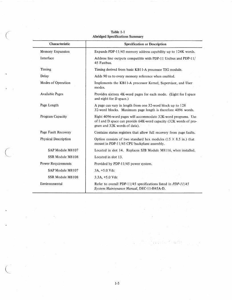
Table 1-1 Abridged Specifications Summary
Specification or Description
Expands PDP-l 1/45 memory address capability up to l24K words.
Address line outputs compatible with PDP-II Unibus and PDP-l 1/ 45 Fastbus.
Timing derived from basic KB 1 I-A processor TIG module.
Adds 90 ns to every memory reference when enabled.
Implements the KBII-A processor Kernel, Supervisor, and User modes.
Provides sixteen 4K-word pages for each mode. (Eight for I space and eight for D space.)
A page can vary in length from one 32-word block up to 128 32-word blocks. Maximum page length is therefore 4096 words.
Eight 4096-word pages will accommodate 32K-word programs. Use of I and D space can provide 64K-word capacity (32K words of program and 32K words of data). '
. .
Contains status registers that allow full recovery from page faults.
Option consists of two standard hex modules (15 X 8.5 in.) that mount in PDP-l 1/45 CPU backplane assembly.
Located in slot 14. Replaces SJB Module M8lI6, when installed.
Located in slot 13.
Provided by PDP-I 1/45 power system.
3A, +5.0Vdc
3.3A, +5.0 Vdc
Refer to overall PDP-II /45 specifications listed in PDP-ll /45 System Mainte.nance Manual, DEC-lI-H45A-D.
1-5


c
CHAPTER 2
OPERATION AND PROGRAMMING
This chapter describes the relocation, protection, and abort mechanisms of the KTII-C, all registers available to
the programmer, and operating hints and procedures.
2.1 BASIC KTll-C MECHANISMS
2.1.1 Address Relocation Mechanism
The current processor mode (Kernel, Supervisor, or User) bits (bits 14 and 15 in the processor status word) select
one of three sets of 16 registers to serve as the page base on the current access. The logic, in combination with
the PDP-l 1/45 processor address, selects either the subset of eight instruction base registers or the subset of eight
data base registers within the set. All instructions, index words, absolute addresses, and immediate operands use
the instruction base registers. All other references use the data base registers. Bits 13, 14, and 15 of the proces
sor address are then employed as a 3-bit encoded index into the eight register subsets previously selected. This.
encoded index selects a specific base (relocation) register, and thus for each memory reference, one of 48 base
registers is selected to perform the address relocation.
The content of the selected base register is an initial or base value in the physical address space. The base value
is always a multiple of 32 words; as a result, the lowest 6 bits of the base address (bit 0 specifies byte address on
the PDP-II) are always O. In actuality, only the upper 12 bits of the base address are stored in the base registers
because the lower 6 bits are by implication O.
To form the final physical address, a displacement from the base specified by the lowest 13 bits of the processor
address (the upper 3 bits have been stripped off as an index into the base registers) is added to the base value con
tained in the base register. Note that this mapping technique allows pages of variable length (32 to 4096 words)
to be packed efficiently in physical memory. Also note that the use of pages with less than 4096 words will re
sult in discontiguous virtual address spaces because in the virtual address space a page begins on a 4096-word
boundary.
As a specific example consider program A, starting address 0, is relocated by the constant 6400, which provides
an address of 6400 (Figure 2-1). If the next processor virtual address is 2, the relocation constant will then cause
physical address 64028 , which is the second item of program A to be accessed. When program B is running, the
relocation constant is changed to 10008 , Then program B virtual addresses starting at 0 are relocated to access.
physical addresses starting at 1000008 , Using the active page address registers to provide relocation eliminates
the need to "relink" a program each time it is loaded into a different physical memory location. To the proces
sor, the program always appears to start at the same address. Note that the base address is stored in a Page Ad
dress Register (PAR).
2-1

1 OF 48 {
DATA
8ASE REGISTERS SELECTED KERNEL/SUPER/ {
USER MODE
PHYSICAL ADDRESS
PROCESSOR VIRTUAL ADDRESS A
Figure 2-1 Basic KT1l-CRelocation Mechanism
11-1211
The relocation example shown in Figure 2-2 illustrates. several points about memory relocation. These points are:
a. Although the program appears to be in contiguous address space to the processor, the 32K-word virtual address space is actually relocated to several separate areas of physical memory. As long as the total ava:ilable physical memory space is adequate, a program can be loaded. The physical memory space need not be contiguous.
b. Pages may be relocated to higher or lower physical addresses, with respect to their virtual address ranges .. In Figure 2-2, page 1 is relocated to a hi~er range of physical addresses, page 4 is relocated to a lower range, and page 3 is notrelocated at all (even though its relocation constant is non-zero).
c. All of the pages in the example start on 32-word boundaries.
d. Each page is relocated independently. There is no reason two or more pages could not be relocated to the same physical memory space. Using mote than one page address register in the set to access the same space is. one way of providing different memory access rights to the same data, depending on which part of a program was referencing that data. Further information on memory protection is provided in Paragraph 2.1.2. In Figure 2-2, note thatthe same relocation constant is assigned to Pages 4 and 6. As a result, virtual addresses within both address ranges access the same physical addresses in memory, using separate page .address registers ..
When the KT1l-C Memory Management Unit option is added to the PDP-l 1/45 system, the l6-bit KBll-A address output is no longer interpreted as the direct physical address of a device or a memory location. Instead, it is considered a l6-bi~ virtual address that contains information to be used by the KT1l-C to construct an l8-bit physical address. Figure 2-3 shows how the l8-bit physical address is constructed. Virtual address bits (15: 13) are interpreted as an active page field to select one of eight page registers in a set. Virtual address bits <12:06) provide the block number (0 to 1778 ) within the page; VA (05:00) indicate the displacement within each 32-
word block. The Page Address Register (PAR) contains a Page Address Field (PAF) that is written into the PAR under program control when the program page is defmed. Consider the P AF as the base address of the page.
2-2
(
c
(

c
(
The block number, VA <12:06), is added to the base address PAF <11 :00> to provide the 12 most significant bits
of the physical address. This address and virtual address bits VA <05: 00> (unchanged by relocation) form the lSbit physical address.
PROCESSOR KT11-C MEMORY
VIRTUAL ADDRESS PAGE RELOCATION PHYSICAL RANGES NO. CONSTANT ADDRESSES
160000- 177776
140000- 157776
0 400000 417776 }
320000 400000 PAGE 0
120000- 137776
100000- 117776
2 250000 337776 } PAGE 1
3 060000 320000
060000- 077776
040000 - 057776
4 020000 267776 } PAGE 2
5 100000 250000
020000 - 037776
000000- 017776
6 020000 167776 } PAGE 7 7 150000 150000
117776 .} 100000 PAGE 5
077776 } 060000 PAGE 3
037776 } PAGES 020000 AS. 6
000000
Figure 2-2 Relocation of a 32K-Word Program into 1 24K-Word Physical Memory
15 13 12 0605 16-BIT VIRTUAL ADDRESS
·1 i BLOCK
! WORD FROM: PROCESSOR APF NUMBER NUMBER EXAMPLE: 157746 8
APF SELECTS PAGE ADDRESS REGISTER (PAR)
EXAMPLE: APF=110 VA<12:06> SELECTS
EXAMPLE: 1778 PAR 6 PAGE ADDRESS FIELD
1 EXAMPLE: 54608
r
11-1028
00
I
PAF<17:06> = VA<05:00> BASE ADDRESS OF PAGE IS NOT y, CHANGED
0 1 0 0 0 0 0 01
FULL ADDER L
18-BIT PHYSICAL ADDRESS 11 0 1 0 1 0 1 0 0 1 0 1
EXAMPLE:5657468 ~.--------------------------~~------------~. I PA <17:06> VA <05:b0> I TO UNIBUS A ADDRESS DRIVERS· AND TO FASTBUS ADDRESS LINES
11-1027
Figure 2-3 Construction of an IS-Bit Physical Address
2-3

2.1.2 Memory Protection Mechanisms
Three address protection mechanisms in the KTII-C provide non-resident and read-only protection, execute-only
protection, and internal protection for the three processor mode address spaces.
2.1.2.1 Non-Resident/Read-Only Protection - A Page Descriptor Register (PDR) is selected in the same manner as a Page Address Register (PAR). After the selection occurs, three bits from the PDR are decoded as an access
key. If the access rights designated by the key are inconsistent with the current memory reference, the memory
reference is not completed and an abort to Kernel D space 250 occurs.
When the access key is set to 0, the page is defined as~non-resident, and an immediate abort prevents any attempt by a program to access a non-resident page. Using this feature to provide memory protection, only those pages associated with the current program are set to legal access keys. The access control keys of all other program pages are set to 0, which prevents illegal memory references.
The access control key for a page can be set to 2, allowing read (fetch) memory references to the page but immediately aborting any attempt to write into the page: This read-only type of memory protection can be afforded to pages that contain common data, subroutines, or shared algorithms. This type of memory protection makes certain that access rights to a given information module are user-dependent, i.e., the access right to a giveninformation module may be varied for different users by altering the access control key.
A Page Address Register in each of the sets (Kernel, User, and Supervisor modes) may be set up to reference the
same physical page in memory and each may be keyed for different access rights. For example, the User access
control key might be 2 (read-only access), the Supervisor access control key might be 0 (non-resident), and the Kernel access control key might be 6 (allowing complete read/write access).
2.1.2.2 Execute-Only Protection - The execute-only type of memory protection is part of an overall ability to use reentrant software, which prevents excessive use of memory space when a program is provided for several
users. Such programs can be written in two parts. One part contains pure code that is not modified during exe
cution and can be used to simultaneously service any number of users. For example, the pure code portion of
FORTRAN can service multiple FORTRAN users. A separate second part of the program belongs strictly to
each user and consists of the code and data that is developed during the compiling process. This portion is stored in a separate page of memory. Figure 2-4 shows a comparison of memory space for non-reentrant and reentrant systems.
The KTII-C hardware can differentiate between pure code memory references (which are instructions, immediate operands, index words, and absolute addresses) and all other memory references. When this feature is enabled under program control, the KTII-C will take the "pure code" portion of such a program from an I (instruction) space page. All other data
will be put in~o an associated D (data) space page. Any illegal attempt by an unauthorized user toread from the executeonly I space will be relocated to a separate D space page. Be-
cause the I and D space pages have separate PDRs, access control can be keyed differently for each page. For example, the
D space access control key could be set to ° to cause a non-
FORTRAN FORTRAN COMPILER 1 PURE CODE
FORTRAN USER 1
COMPILER 2 USER 2
FORTRAN USER 3
COMPILER 3 ~SPACE SAVE9~
NON-REENTRANT REENTRANT
11-1034
Figure 2-4 Comparison of Non-Reentrant and Reentrant Program Space Requirements
resident abort, or, as an alternative, the base address of the D space page could be set up to map over some other part of a user's program. In any case, the D space PDR must not be set so that a user can write into the pure
code I space. The difference between the read-only protection described in Paragraph 2.1.2.1 and execute-only
2-4
(
(
protection is that the contents of execute-only pages cannot be read as data. This feature is particularly useful
in protecting proprietary programs from some users. Paragraph 2.4.6 describes I and D space more fully.
In the special case when in User mode and the previous mode specified by the processor status is also User mode,
the action of the MFPI instruction is modified so that the read is via the D relocation registers. In this manner,
the integrity of the execute-only mode is reserved.
2.1.2.3 Multiple Address Space Protection - The three completely separate PAR/PDR sets provided by the
KTII-C for each mode of processor operation (Kernel, Supervisor, and User) give the timesharing system another
type of memory protection. The mode of operation is specified by the Processor Status Word current mode field.
The active page register sets are enabled as follows:
PS (15:14)
00 01 10 11
PAR/PDR Set Enabled
Kernel mode Supervisor mode Illegal (all references aborted) User mode
Thus, a User mode program is relocated by its own PAR/PDR set, as are Kernel and Supervisor programs. It is
therefore impossible for a program running in one mode to accidentally reference space allocated to another
mode when the active page registers are set correctly by a monitor program. For example, a user cannot transfer
to Supervisor or Kernel space. The Supervisor mode address space may be reserved by the system to accommo
date resident compilers, utility programs, and other shared resource programs. The Kernel mode address space
may be reserved for resident system monitor functions, such as the basic Input/Output Control (IOC) routines,
memory management trap handlers, abort handlers, and timesharing scheduling module. By dividing the types
of timesharing system programs functionally between the Kernel, Supervisor, and User modes, a minimum
amount of space control housekeeping is required as the timeshared operating system sequences from one user
program to the next. For example, only the User PAR/pDRset needs to be updated as each new user program is
serviced. The three PAR/PDR sets implemented in the KTlI-C Memory Management lJnit option are shown in Figure 2-5.
2.1.3 Memory Management Statistics Mechanism
A timeshared system swaps programs or parts of programs in and out of memory using secondary storage facili
ties such as disk or drum systems. In a swapping environment, the operating system must provide the software
routines that decide what programs should be swapped and when and how these programs can be swapped be
tween memory and secondary storage. The operating system routines can be simple or complex depending on
system requirements, e.g., the amount of overhead time that can be tolerated. The operating system may also
have to decide which active page is least likely to be required in the immediate future and may therefore be
swapped out to make memory space available for a new program. To make such a memory management deci
sion, the operating system requires statistics on the use of active pages. Some indication of whether a program , . ,., "; '.,':, '
has been modified during its residence in memory is also desirable. If it has been modified, the modified pro-
gram must be swapped (re-written) into secondary storage. If no modification has been made and the program
can always be re-called from secondary storage, the space it occupies in memory can be overlayed without swap
ping delay. TheKTlI-C logic provides the kind of information required by an operating system to gather mem
ory management statistics on the use of active pages. The availability of this information in the hardware re
duces the overhead time of any routine, simple or complex, in the efficient management of memory. In the
2-5

KTII-C, the Page Descriptor Register associated with each
active page includes a W (written into) and an A (attention)
bit. When any active page is written into, the W bit is set
by the logic; therefore, by testing the W bit the memory
management software routine can decide whether a page
can be overlayed or if it needs to be swapped out.
The A bit has several uses. To use this feature the system
progr¥llmer first enables the memory management trap logic. He can then set the access control keys of the active
pages of interest for special trap conditions. Access control keys are provided to cause:
a. Memory management trap on read (including instruction fetch)
b. Memory management trap on write
c. Memory management trap on read or write.
Then, the A bit for the active page is set when the page is
accessed as specified and a resultant memory management
trap occurs. The vector at trap location 250 Kernel address
space causes the operating system routine to service the
memory management trap. The routine can test the A bit
to accumulate statistics on the use of that page. When a
swapping decision is required of the operating system, these
statistits can be examined to determine the more active
,pages (which might therefore be retained in memory).
2.1.4 Trap/Abort Mechanism
0 1 2 3 4 5 6 7
0 1 2 3 4 5 6 7
0 1 2 3 4 5 6 7
KERNEL PAR IPDR REGISTERS I SPACE D SPACE
0
2 3 4 5 6 7
PAR PDR PAR PDR
SUPERVISOR PAR/PDR REGISTERS
I SPACE D SPACE 0 1 2 3 4 5 6 7
P.AR PDR PAR PDR
USER PAR/PDR REGISTERS I SPACE D SPACE
0 1 2 3 4 5 6 7
PAR PDR PAR PDR
"11-1029
Figure 2-5 KTlI-C Memory Management Unit PAR/PDR Registers
Memoty references that violate the protection keys set in the KTII-C cause an interrupt in the processor. The
interrupt process is described in Paragraph 5.3 of the PDP-ll/45 Handbook. In KTII-C aborts and traps, the
new PC for the abort/trap service routine is taken froin 250 in Kernel virtual D space, while the new PS is taken
from 252. No other interrupts use 250 as a trap vector. Note that both abort and statistical traps are taken to
250.
Non-resident, read-only, and page length violations cause an interrupt to the processor before the reference is
made. Memory management traps occur only at the end of complete instructions. Paragraphs 3.11.1 and 3.11.2
describe the trap/abort logic and include two system diagrams that inditate how the interrupt is implemented in
the logic. The order of interrupt service is listed in Appendix C of the PDP-ll /45 Processor Handbook.
2.2PARjPDR REGISTERS
The contents of the Page Address Register (PAR) and the Page Descriptor Register (PDR) describe a memory
page.
The KTlI-C provides three sets of 16 PAR/PDR pairs. As indicated in Figure 2-5, one PARjPDR set is used to
reference memory while the processor is in Kernel mode, another in Supervisor mode, and the third in User
mode. Each set is subdivided into two groups: one for reference to instruction (I) space and one for reference
to data (D) space. Figure 2-5 shows the organization of the three sets. Each pair consists of a Page Address
2-6
(
C
(

( Register (PAR) and a Page Descriptor Register (PDR). These registers are always used as a pair and contain all
the information required to locate and describe the current active pages for each mode of operation.
The current mode bits (bits 14 and 15) of the Processor Status Word determine which set will be referenced for
each memory access. A program operating in one mode cannot use the P AR/PDR sets of the other two modes
to access memory. Thus, the three sets are a key feature in providing a fully protected environment for a time
shared multiprogramming system. The virtual address value determines which page within a set is to be used.
This correspondence is listed below:
Page No.
o 1 2 3 4 5 6 7
Virtual Addresses
000000 - 017777 020000 - 037777 040000 - 057777 060000 - 077777 100000 - 117777 120000 - 137777 1'40000 - 157777 160000 - 177777
Finally the use of the reference (part of an instruction or data access) determines whether the I space P AR/PDR
set or the D space PAR/PDR set is used. Each PAR and PDR of every set is:assigned to a specific processor I/O
address. Table 2-1 is a complete list of address assignments.
NOTE Unibus devices cannot access PARs or PDRs.
In a fully-protected multiprogramming environment, only a program operating in Kernel mode would be allowed
to access the PAR and PDR locations for the purpose of mapping a user's programs. However, there are no re
straints imposed by the KTll-C logic that will prevent Supervisor or User mode programs from accessing these
registers. The option of implementing such a feature in the operating system and thus explicitly protecting these
locations from user's programs is available to the system software designer.
2.2.1 Page Address Registers (PAR)
The Page Address Register (PAR) shown in Figure 2-6 contains the base address of the page in the form of a 12-
bit Page Address Field (PAF). Bits 15-12 of the PAR are not implemented in the hardware.
The PAR can also be thought of as a relocation register containing a relocation constant or as a base register con
taining a base address. Either interpretation indicates the basic function of the PAR in the relocation scheme.
Note that thePAF is interpreted in address calculations as a multiplier of 32, i.e., when used as a base register,
the lowest 6 bits are assumed to be O. The bit stored in bit 0 of the PAF becomes bit 6 of the page base address,
bit 1 of the P AF, bit 7 of the page base address, etc. Thus, bit 11 of the PAF becomes bit 17 of the page base
address.
11
PAGE ADDRESS FIELD (PAF)
o
11-1036
Figure 2-6 Page Address Register (PAR) Format
2-7

Table 2-1 PAR/PDR Address Assignments
Kernel
I Space D Space
No. PAR PDR No. PAR PDR
0 772340 772300 0 772360 772320 1 772342 772302 1 772362 772322 2 772344 772304 2 772364 772324 3 772346 772306 3 772366 772326 4 772350 772310 4 772370 772330 5 772352 772312 5 772372 772332 6 772354 772314 6 772374 772334 7 772356 772316 7 772376 772336
Supervisor
I Space D Space
No. PAR PDR No. PAR PDR
0 772240 772200 0 772260 773220 1 772242 772202 1 772262 773222 2 772244 772204 2 772264 773224 3 772246 772206 3 772266 773226 4 772250 772210 4 772270 773230 5 772252 772212 5 772272 773232 6 772254 772214 6 772274 773234 7 772256 772216 7 772276 773236
User
I Space D Space
No. PAR PDR No. PAR PDR
0 777640 777600 0 777660 777620 1 777642 777602 1 777662 777622 2 777644 777604 2 777664 777624 3 777646 777606 3 . 777666 .777626 4 777650 777610 4 777670 777630 5 777652 777612 5 777672 777632 6 777654 777614 6 777674 777634 7 777656 777616 7 777676 777636
2.2.2 Page Descriptor Registers (PDR)
The Page Descriptor Register (PDR) contains page expansion, direction, page length, and access control (Figure 2-7).
2-8
(
(,

c
(
PAGE LENGTH FIELD (PLF)
11 -1037
Figure 2-7 Page Descriptor Register (PDR) Format
2.2.2.1 Access Control Field (ACF) - The ACF is a 3-bit field (occupying bits 2-0 of the PDR) that describes the access rights to this particular page. The access codes or "keys" specify the manner in which a page may be accessed and whether. or not a given access should result in a trap or an abort of the current operation. A memory reference that causes an abort is not completed and is terminated immediately. Hence an aborted "read" reference does not obtain any data from the location, and an aborted "write" reference does not change the data in the location. A memory reference that causes a trap is completed. When a memory reference causes a trap, the trap does not occur until the entire instruction has been completed. Aborts are caused by atfempts to access non-resident pages, page length errors, or access violations, such as attempting to write into a read-only page;
Traps are used as an aid in gathering memory management information.
In the context of access control, the term write is used to indicate the action of any instruction that modifi~s
the contents of any addressable word. A write is synonymous with what is usually termed a store or modify in many computer systems. Table 2-2 lists the ACF keys and their functions. The ACF is written into the PDR
under program control.
Table 2-2 Access Control Field Keys
AFC Key Description Function
000 0 Non-resident (NR) Abort any attempt to access this non-resident page.
001 1 Read only and trap (RROT) ,
Trap to. location 250 in Kernel D space after read. Abort any attempt to write into this page.
010 2 Resident read only (RRO) Abort any attempt to write into this page.
011 3 Illegal Unused. Reserved for future use. Abort any access attempt.
100 4 Resident read/write and trap Memory management trap to location 250 in Ker-(RRWT) nel D space upon completion of a read or write to
this page.
101 5 Resident read/write and trap Allows read/write of page and traps to location 250 when write (RRWTW) in.Kernel D.space upon completion of a write.
110 6 Resident read/write (RRW) Read or write allowed. No trap or abort occurs.
111 7 Illegal Unused. Reserved for future use. Abort any access attempts.
2.2.2.2 Expansion Direction (ED) - The ED bit located in PDR bit position 03 indicates the authorized direc
tion in which the page expands. A logic 0 in this bit (ED = 0) indicates that the page expands upward from relative zero (page base address). A logic lin this bit (ED = 1) indicates that the page expands downward toward
relative zero (page base address). The ED bit is written into the PDR under program control. When expansion is upward (ED = 0), the page length is increased by adding blocks with higher relative addresses. Upward
2-9 -----
/

expansion is usually specified for program or data pages to add more program or table space. An example of page expansion upward is shown in Figure 2-8.
PAR PDR
1000 001 111 000 I 10 0101001 0000 0110 I
PAF=Ol~ __ :r 1J PLF = 518 = 41'O=BLOCK NO. _
ED = 0 = UPWARD EXPANSION
ACF=6= READ/WRITE
NOTE' TO SPECIFY 42-BLOCK PAGE LENGTH FOR AN UPWARD EXPANDABLE PAGE. WRITE HIGHEST AUTHORIZED BLOCK NO. DIRECTLY INTO HIGH BYTE OF PDR. BIT 15 IS NOT USED BECAUSE THE HIGHEST ALLOWABLE BLOCK NUMBER IS 177B
ADDRESS RANGE OF POTENTIAL PAGE -
EXPANSION BY CHAN GING THE PLF
AUTHORIZED PAGE LENGTH = 4210 BLOCKS
024176 BLOCK 518
024100
017276 BLOCK 2
017200
017176 BLOCK 1
017100
017076 BLOCK 0
017000
ANY BLOCK NUMBER GREATER THAN 4110 (51 8)
(VA<12:06» 51 8 )
WILL CAUSE A PAGE LENGTH ABORT.
E ADDRESS OF PAGE
11-1030
Figure 2-8 Example of an Upward Expandable Page
When expansion is downward (ED = 1), the page length is increased by adding blocks with lower relative addresses.
Downward expansion is specified for stack pages so that more stack space can be added. An example of page ex
pansion is shown in Figure 2-9. Paragraphs 2.5.3 and 2.5.4 provide a description of the interaction of the ED bit
with the Page Length Field (PLF).
2.2.2.3 Written Into (W) - The W bit located in PDR bit position 06 indicates whether the page has been writ
ten into since it was loaded into memory. W = 1 is affirmative. :Note that the W bit is set independent of the ACF key and the memory management enable bit (bit 9) in SRO. The W bit is automatically cleared when either
the PAR or PDR of a page is written into. It can only be set by KT11-C contro11ogic.
2-10
(
(
(

(
c
!--ACTIVE PAGE REGISTER CONTENTS~ PAR PDR --l
10000011110001 010101100000 1 110
~ '-------.----'
:~:: ~~::. 86 10 I I ED' l' DOWNWARD EXPANSION ---------'
TO SPECIFY PAGE LENGTH FOR A DOWNWARD EXPANDABLE PAGE, WRITE COMPLEMENT OF BLOCKS REQUIRED INTO HIGH BYTE OF PDR,
IN THIS EXAMPLE,A 42-BLOCK PAGE IS REQUIRED. PLF IS DERIVED AS FOLLOWS: 4210' 528 ;TWO'S COMPONENT· 1268 •
AUTHORIZED PAGE LENGTH'421O BLOCKS
ADDRESS RANGE
036776 BLOCK 1778
036700
036'676 BLOCK 1768
036600
0311676 BLOCK 1268
0311600
031676 BLOCK 1268
031600
A BLOCK NUMBER REFERENCE LESS THAN 1268
OF POTENTIAL PAGE ~~~~~~~ EXPANSION BY ~
CHANG ING THE PLF ~~~~~@~ (VA < 12: 06> LESS THAN 1268) WILL CAUSE A PAGE LENGTH ABORT,
- BASE ADDRESS OF PAGE
11-1031
Figure 2-9 Example of a Downward Expandable Page
In disk swapping and memory overlay applications, the W bit can be used to determine the pages in memory that
have been modified by a user. Those that have been written into must be saved in their current form; those that
have not been written into (W = 0), need not be saved and can be overlayed with new pages if necessary.
NOTE The W bit cannot be set by a memory access of a KTII-C internal register or a memory access that causes an abort.
2-11
2.2.2.4 Attention (A) - The A bit located in PDR bit position 07 indicates whether any memory page accesses
caused memory management trap conditions to be true. A = 1 is affIrmative. Trap conditions are specified by
the ACF. The following conditions will set the A bit.
1. ACF = 001 and read reference. 2. ACF = 100. I
3. ACF = 101 and write reference.
Note that the A bit is set independent of the memory management enable bit (bit 9) in SRO. The A bit is used
in the process of gathering memory management statistics for the purpose of optimizing memory use. The A bit
is automatically cleared when the PAR or PDR of the page is written into. It can only be set by the KT ll-C con
trollogic.
NOTE The A bit cannot be set by a memory access of a KTII-C internal register or a memory access that causes an abort.
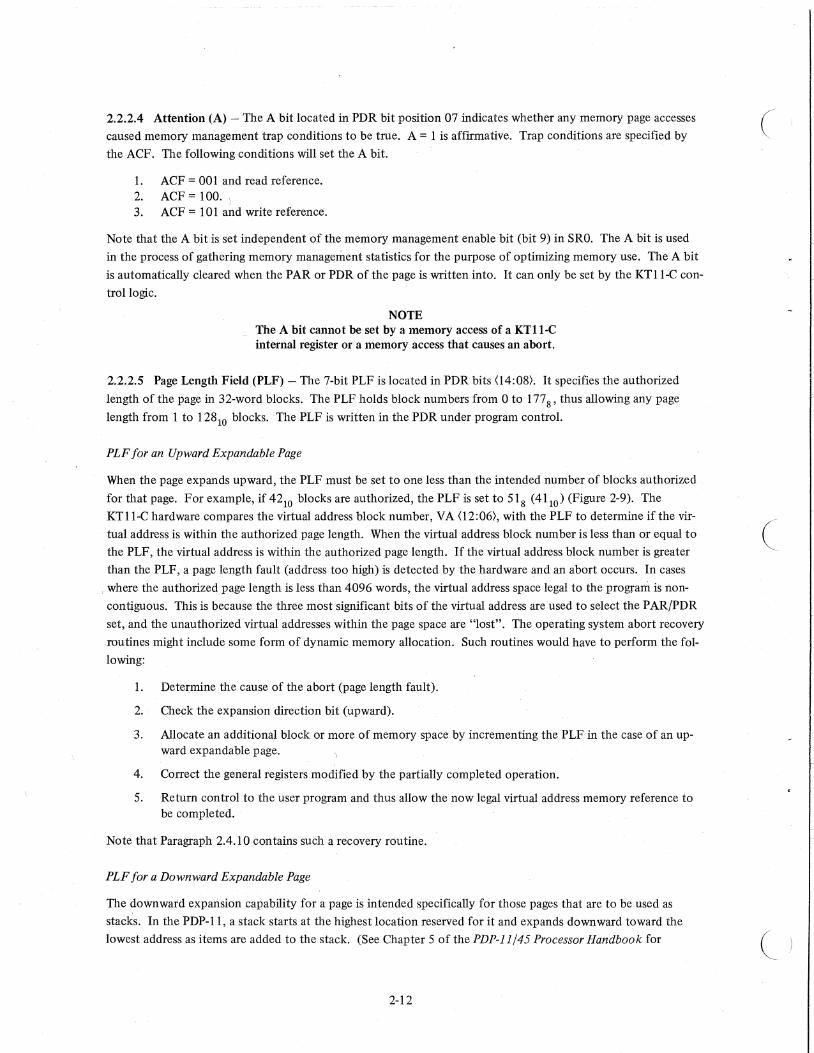
2.2.2.5 Page Length Field (PLF) - The 7-bit PLF is located in PDR bits <14:08). It specifies the authorized
length of the page in 32-word blocks. The PLF holds block numbers from 0 to 1778, thus allowing any page
length from 1 to 12810 blocks. 'The PLF is written in the PDR under program control.
PLF for an Upward Expandable Page
When the page expands upward, the PLF must be set to one less than the intended number of blocks authorized
for that page. For example, if 4210 blocks are authorized, the PLF is set to 518 (41 10 ) (Figure 2-9). The
KT11-C hardware compares the virtual address block number, VA <12:06), with the PLF to determine if the vir
tual address is within the authorized page length. When the virtual address block number is less than or equal to
the PLF, the virtual address is within the authorized page length. If the virtual address block number is greater
than the PLF, a page length fault (address too high) is detected by the hardware and an abort occurs. In cases
c where the authorized page length is less than 4096 words, the virtual address space legal to the prograni is non
contjguous. This is because the three most significant bits of the virtual address are used to select the PARjPDR
set, and the unauthorized virtual addresses within the page space are "lost". The operating system abort recovery
routines might include some form of dynamic memory allocation. Such routines would have to perform the fol
lowing:
1. Determine the cause of the abort (page length fault).
2. Check the expansion direction bit (upward).
3. Allocate an additional block or more of memory space by incrementing the PLF in the case of an upward expandable page.
4. Correct the general registers modified by the partially completed operation.
5. Return control to the user program and thus allow the now legal virtual address memory reference to be completed.
Note that Paragraph 2.4.10 contains such a recovery routine.
PLF for a Downward Expandable Page
The downward expansion capability for a page is intended specifically for those pages that are to be used as
stacks. In the PDP-II, a stack starts at the highest location reserved for it and expands downward toward the
lowest address as items are added to the stack. (See Chapter 5 of the PDP-ll /45 Processor Handbook for
2-12
(
c

(
c
complete details.) When the page is to be downward expandable, the PLF must be set to authorize a page length,
in blocks, that starts at the highest address of the page, i.e., always block 1778 , Figure 2-10 shows an example
of a downward expandable page. A page length of 4210 blocks is arbitrarily chosen so that the example can be compared with the upward expandable example shown in Figure 2-9.
NOTE The same PAF is used in both examples to emphasize that the P AF, as the base address, always determines the lowest address of the page, whether it is upward or downward expandable.
PAGE THAT SET ABORT ERROR FLAGS
15 14 13 12 11 10 9 8 7 6 5 4 3 2 1 0
111111111: II:: II
ABO:~~::~:o~~::~~~~: ~ r r 1.· T 1 ~. ABORT: READ ONLY VIOLATION ~ _
TRAP:MEMORY MANAGEMENT
TRAP:OPERATING ______ --'
ADDRESS: 777572
ENABLE KTll-C
PAGE NUMBER
ADDRESS SPACE liD
MODE OF OPERATION
INSTRUCTION COMPLETE
SYSTEM TESTER L-____________ MAINTENANCE MODE
ENABLE MEMORY MANAGEMENT TRAPS -----------' 11-1038
Figure 2-10 Format of Status Register 0 (SRO)
To calculate the value to be placed in the PLF for a downward expandable page proceed as follows.
Take the number of 32-word blocks to be authorized and create the negative of it in 2's complement notation.
The 2's complement is formed by negating each binary bit, then adding 1 to the result.
Example:
528 bit negation add
1268
0101010 1010101
1010110
The same dynamic memory allocation routine can be used to recover from a page length abort. After determin
ing that the page was downward expandable, the PLF would be decremented to allow downward expansion.
2.3 MEMORY MANAGEMENT STATUS REGISTERS
Aborts and traps generated by the KT1l-C logic are vectored through Kernel D space address location 250. Sta
tus Registers SRO, SRI, and SR2 can be referenced by fault recovery routines to differentiate between an abort
and a trap, determine why the abort or trap occurred, perform the service routines required to recover from the
abort or handle the trap, and allow for program restart. The following paragraphs describe the formats of each status register.
2-13
2.3.1 Status Register 0 (SRO)
SRO contains abort error flags, memory management enable and trap flag bits, plus other essential information
required by an operating system to recover from an abort or to service a memory management trap. The physi
cal address of SRO is 777572. The SRO format is shown in Figure 2-10.
Bits 15-11 are the abort and trap flags, and can be considered to be in a "priority queue" in that "flags to the
right" are less significant and should be ignored. For example, a "non-resident" abort service routine would ig
nore page length, access control, and memory management flags. A "page length" abort service routine would
ignore access control and memory management faults.
NOTE Bits 15, 14, or 13, when set (abort conditions) cause the KTll-C logic to freeze the contents of SRO bits 1-7 and status registers SRI and SR2 to facilitate recovery from the abort.
The error flag bits 15-12 are enabled when an address is being relocated by the KT Il-C. This implies that either
SRO, bit ° is equal to 1 (KTll-C operating) or that SRO, bit 8 is equal to 1 and the memory reference is the final
one of a destination calculation (maintenance/destination mode).
Note that SRO bits 0, 8, and 9 can be set under program control to provide meaningful memory management
control information. However, information written into all other bits is not meaningful. Only that information
automatically written into these remaining bits as a result of hardware actions is useful as a monitor of the status
of the memory management unit. Setting bits 15 -11 under program control will not cause aborts or traps to
occur. Bits 15-11 must be reset to ° after an abort or trap has occurred in order to resume monitoring memory
management. Setting bits 15, 14, or 13 will, however, freeze the contents of SRO bits (1 :7), Status Register 1
(SRI) and Status Register 2 (SR2).
2.3.1.1 Abort-Nonresident - Bit 15 is the "Abort-Nonresident" bit. It is set by attempting to access a page
with an access control field (ACF) key equal to 0, 3, or 7.
2.3.1.2 Abort-Page Length - Bit 14 is the "Abort Page Length" bilt. It is set by attempting to access a location
in a page with a virtual address block number (Virtual Address bits (12: 06») that is outside the area authorized by the Page Length Field (PLF) of the PDR for that page. Bits 14 and 15 of SRO may be set simultaneously by the
same access attempt.
2.3.1.3 Abort-Read Only - Bit 13 is the "Abort-Read Only" bit. It is set by attempting to write in a page with
an access key of 1 or 2.
2.3.1.4 Trap-Memory Management - Bit 12 is the "Trap-Memory Management" bit. It is set by a read opera
tion that references a page with an ACF key of 1 or 4 and by a write operation with an;ACF key of 4 or 5. The
functions of these ACF keys are listed in Table 2-2. Note that the "Enable Memory Management" bit (SRO, bit
9) must be a 1 for the "Trap-Memory Management" bit to be set.
2.3;1.5 Bit 11 ~ Bitll is a spare flag reserved for future use.
2-14
(

(
c
2.3.1.6 Enable Memory Management - Bit 9 is the "Enable Memory Management" bit. It can be set or cleared
by domg a direct write mto SRO. If bit 9 is cleared, no memory management traps can occur. The A and W bits will, however, contmue to log potential memory management traps. When bit 9 is set to 1, the next memory management trap condition will cause a trap, vectored 'through Kernel D virtual address 250.
NOTE If the instruction thatc1ears bit 9 (to disable memory management) causes a potential memory management trap in the course of any of its memory references prior to the one actually changing SRO, the trap will occur at the end of the instruction.
2.3.1.7 Maintenance/Destination Mode - Bit 8 specifies maintenance use of the memory management unit. It
is used for KTII-C diagnostic purposes. For the instructions used in the mitial diagnostic program, bit 8 is set so that only the final destination reference is relocated. This bit must not be used for other purposes.
2.3.1.8 Instruction Completed - When an abort has occured, bit 7 mdicates that the current mstruction has been completed and that the current memory references are caused by an interrupt or "T" bit, Parity, Odd Address or Timeout traps.
2.3.1.9 Abort Recovery Information - When an abort occurs, bits (1 :6) of SRO cOhtain the mformation neces
sary to determme which of the 48 pages caused the abort. Specifically, bits (1 :6) contain the processor mode, whether I or D space, and which 4K page within mode-space.
Mode of Operation
Bits 5 and 6 indicate the CPU mode (User/Supervisor/Kernel) associated with the page causmg the abort or trap
(Kernel = 00, Supervisor = 01, User = II). These bits are controlled by the KT1I-C logic that decodes current
previous mode bits of the PSW.
Address Space liD
Bit 4 mdicates the type of space (lor D) being accessed (0 = I Space, 1= D Space). It is controlled by the
KT1I-C logic that selects I/D space.
Page Number
Bits 3-1 contain the page number of a reference. Pages, like blocks, are numbered from 0 upwards. The page number and address space bits are used by the error recovery routme to identify the page being accessed if an
abort occurs.
2.3.1.10 Enable KTII-C - Bit 0 is the "Enable KT ll-C" bit. When it is set to· 1, all addresses are relocated and protected by the memory management unit. When bit 0 is set to 0, the memory management unit is disabled and
, addresses are neither relocated nor protected. Note that with this bit 0, all programs that run on the PDP-l 1/20
will run on the PDP-l 1/45.
2.3.2 Status Register 1 (SRI)
SRI records any automcrement/autodecrement of the general purpose registers, excluding implicit changes to
the PC. The physical address of SRI is 777574. SRI is cleared at the beginnmg of each mstruction fetch and interrupt. When a general register is automcremented or auto decremented, the register number and the amount
2-15

(in 2's complement notation) by which the register was modified is written into SRI (Figure 2-1l). The information contained in SRI is necessary to accomplish an effective recovery from an abort. The low order byte is written first, and it describes the first general register that was changed. If a second general register is changed by the instruction, that change information is written into the high order byte of SRI. It is not possible for a
PDP-II instruction to autoincrement/autodecrement more than two general registers per instruction before an "abort-causing" reference. Because only three bits are provided for the general register number, it is up to the
software to determine which set of registers (User/Supervisor/Kernel-General Set a/General Set I) was modified by deter~ng the CPU and Register modes as contained in the Processor Status Word (PSW) at the time of the
abort. SRI is read-only; a write attempt will not modify its contents.
2.3.3 Status Register 2 (SR2)
SR2 is loaded with the 16-bit Virtual Address (VA) at the beginning of each instruction fetch, or with the address Trap Vector at the beginning of an interrupt; "T Bit" trap, Parity, Odd Address, and Timeout traps are also
loaded with the trap vector. The physical address of SR2 is 777576. SR2 is read~only; a write attempt will not
modify its contents. SR2 is the Virtual Address Program Counter (Figure 2-12).
III ala lOa ala all SRI EXAMPLE 172423
. U' "----.L--'TL Register 3 L- was incremented by 2.
Register 5 was decremented by 2.
15 11 10 8 7 3 2 o
AMOUNT CHANGED REGISTER AMOUNT CHANGED REGISTER (2' S COMPLEMENT) NUMBER (2'S COMPLEMENT) NUMBER
Figure 2-11 Format of Status Register I (SRI)
15 o
16-BIT VIRTUAL ADDRESS
Figure 2-12 Format of Status Register 2 (SR2)
2-16
ADDRESS: 777574
11-1039
ADDRESS: 777576
11-1040
c
c

c
l
2.3.4 Status Register 3 (SR3)
SR3 is a 4-bit register thaUstores liD space control information. The physical address of SR3 is 712516. Data
can be written into or read from SR3 under program control. The SR3 format is shown in Figure 2-13. When
the ENABLE D SPACE bit for a specific mode (Kernel, Supervisor, or User) is cleared, only the I space PARI
PDR set will be used when operating in that mode. If an ENABLE D SPACE bit is set, then the D space PARI
PDR set for that mode is enabled. Then, if a memory reference is not an instruction fetch, immediate operand, index word, or an absolute address, the D space P AR/PDR set will be used to relocate that memory reference.
15 432 a
SPARE .-J.-J~ KERNEL MODE-----.J
"1" ENABLES { SUPER MODE D SPACE
USER MODE
Figure 2~ 13 Format of Status Register 3 (SR3)
2.4 KTll-C OPERATION
ADDRESS: 772516 8
11-1041
This section contains operational information, including techniques, hints, and cautions. -
2.4.1 Console Operations
When the KT ll-C option is implemented and enabled in the PDP-II 145 system, console operations are effected
as described in the following paragraphs:
2.4.1.1 Single Step Mode - To single step through a program, do not use the console START switch. To do so
will disable the KTlI-C by clearing SRO. As an alternative, load the PC (R7) with the starting address and press the CONT switch.
2.4.1.2 Address Display - When the KT ll-C is enabled, the console address display is determined by the Ad
dress Display Select switch position, as indicated in Table 2-3.
2.4.1.3 Stepping Over 32K-Word Boundaries - On Examine Next and Deposit Next operations a carry is not
propagated from bit 15 to bit 16.
2.4.2 Physical Address Determination
A l6-bit virtual address can specify up to 32K words in the range from 0 to 1777768 (word boundaries are even
octal numbers). The three most significant virtual address bits designate the PAR/PDR set to be referenced dur
ing page address relocation. Table 2-4 lists the virtual address ranges that specify each of thePAR/PDR sets.
To calculate the physical address, disregard the three most significant VA bits and add the remainder to the PAR
contents, left-shifted six places.
2-17

Example:
VA = 167456 = xxxO 100
111 101
100 110
101 110 + (PAR) = 3456 011
PA = 355256 = 011 101 101 010 101 110
Where x indicates these bits are not used in the calculation.
Switch Position
PROGPHY
CONSPHY
USER, SUPER, or KERNEL, I or D
Table 2-3
Address Display Select Switch
Interpretation and Use
Program Physical Address: Physical (relocated) addresses accessed by the program. This position is used for single stepping through the program being relocated. It will always display the actual memory address of the location being accessed.
Console Physical Operations: Used for examines or deposits to a physical address whether the KT ll-C is enabled or not. It will display the address loaded from the console switch register.
Virtual Address: Used for examines or deposits to the virtual address when the current physical location may be unknown. These positions always display the address generated by the KBII-A processor.
NOTE A detailed description of the source of individual address bits is provided in Paragraph 3.5.1.
Table 2-4
Relating Virtual Address to PARIPDR Set
Virtual Address Range PARjPDR Set
000000 - 17776 0 020000 - 37776 040000 - 57776 2 060000 - 77776 3 100000 - 117776 4 120000 - 137776 5 140000 - 157776 6 160000 - 177776 7
2.4.3 Protection Without Relocation
To obtain a one-to-one mapping of virtual address space to physical address space (no relocation), a value must
be placed in each PAR to be accessed, because the three most significant bits of the virtual address are "stripped"
to select the PARjPDR set. Therefore, these three bits must be "mirrored" by the contents of each PAR, as in
dicated in the chart on the following page.
2-18
(
(
(
( PAR Contents
0 000000 000200
2 000400 3 000600 4 001000 5 001200 6 001400 7 001600
NOTE If PAR 7 is to address the I/O page, its contents must be 007600.
2.4.4 Communication Between User/Supervisor/Kernel Address Space
A program in one address space can communicate with a program in another address space using three basic
methods. The simplest method is to make a part of each program common by overlappi:ng physical address space.
A second method is to use the MTPD, MTPI, MFPD, and MFPI instructions. These instructions are defined in
Chapter 4 of the PDP-ll/45 Processor Handbook. A third method is to use the "return from interrupt" (RTI)
instruction. These methods are described in the following paragraphs.
2.4.4.1 Overlapping Physical Addresses - Consider the problem of providing a buffer area to move data to and
from I/O devices through the monitor/file system. Without overlapping, the data would be brought into a buffer
area located in Kernel data space. It would then be moved into a separate buffer area in User space. However,
using KTlI-C memory mapping capabilities, a single buffer area can be located in physical memory with provi
sions for access by User, Supervisor, and Kernel mode programs. This method saves the additional memory space
required for separate buffer areas and also the time required to move data from one buffer area to another.
2.4.4.2 MFPI and MTPD Instructions Use - In the following example, a word is popped off the Kernel stack
and pushed onto the User stack. This method of stack-to-stack communication is typical of well-defined operat
ing system communication. Assume that the processor is running in the Kernel mode.
MFPI R6
MOV (R6) +, Rl
MTPD -(Rl)
;ADDITIONAL WORDS MOVED HERE
MOV Rl,-(R6)
MTPI R6
;GET CURRENT VALUE OF USER STACK. ;PUSH IT ONTO KERNEL STACK. NOTE ;THAT SINCE ALL GENERAL REGISTERS ARE ;IN BOTH I AND D SPACE, THIS INSTRUCTION ;COULD HAVE BEEN "MFPD". ;POP USER R6 VALUE OFF KERNEL STACK. ;PUT IT IN GENERAL REGISTER 1. ;POP ARGUMENT OFF KERNEL STACK. PUT ;IT ON TOP OF USER STACK.
;PUT CORRECTED USER STACK POINTER ON ;KERNEL STACK. ;POP CORRECTED USER R6 VALUE OFF KERNEL ;STACK AND PUT IN USER R6. (INSTRUCTION ;COULD HAVE BEEN "MTPD".)
2-19

The use of MTPI and MFPI is restricted in the User mode. If the previous mode bits (13: 12) of the PS word also
specify User mode (11), then the following restriction is implemented to preserve the integrity of execute-only
protection. The execution of a MFPI will be relocated by the equivalent D space P AR/PDR register set if "D"
space for the User mode is enabled (SR3, bit a = 1). This prevents a user from using MFPI to read from an
execute-only page in his address space.
2.4.4.3 Control Information - CQntrol is passed inward from User and Supervisor modes to' the Kernel mQde
by all traps and interrupts. All trap and interrupt vectors are lQcated in Kernel virtual address space. Thus, all
traps and interrupts pass thrQugh Kernel space to' Qbtain their new PC and PS, and determine the new mQde of
prQcessing. Control is passed outward frQm the Kernel mQde to' the User and SupervisQr mQdes by the RTT and
RTI instructiQns, which restore the Qld PC and PS by PQPping them from the stack.
2.4.5 Statistical Aids Use
Three ACF keys (1, 4, and 5) can cause traps at the end of the current instruction when the Enable MemQry Man
agement Traps bit is set in the SRO. These keys alsO' cause the A bit in the associated PDR to' be set, regardless Qf
whether the Enable MemQry Management Trap bit is set. A PDP-II dQuble Qperand instructiQn can access up to'
six different pages Qf memQry during executiQn. If each Qf the six PDRs had ACF keys that specified memory
management traps, then the A bit in each of the PDRs will have been set by the time the instructiQn is CQm
pleted and the memQry management trap service routine is entered. A statistic gathering service rQutine that CQl
lects "frequency Qf use" data can scan all PDRs and thus gather A bit infQrmation frQm all six PDRs that might
have been set. The status registers are set only Qnce. TherefQre, if the statistical facility is to' collect valid fre
quency Qf use Qn pages, a more elabQrate approach is required of the sQftware service routine.
One approach is to' leave the Enable Memory Management Trap bit reset to 0, so that no traps Qccur, but set the
ACF keys to specify the appropriate traps. This will cause the A bit to' be set. Then, use a real-time clQck to in
terrQgate the A bits. When one is found set, a count 10catiQn corresponding to' that page can be incremented,
and then that A bit must be cleared in the PDR.
One way to clear the A bit is to' write intO' the PDR. FQr example, the instructiQn:
MOV @#PDR, @#PDR
will clear the A and W bits, but leave all other PDR bits unchanged. A less cQmplex way is to' set all read-Qnly
page ACF keys equal to 1 and all read/write page ACF keys equal to' 4. At the end Qf the user time periQd, inter
rogate the A and W bits. MQst state transitiQns with the ACF can be accQmplished by incrementing the PDR;
The ACF keys change as fQllows:
Original ACFKey.
4 5 4
New ACFKey
2 5 6 6
Effect of ACF Key Change
NO' memQry management trap on read. NO' memQry management trap on read. NO' memQry management trap Qn write. NO' memQry management trap Qn a read Qr write.
Thus, by incrementing the ACF key, characteristics of the original key that are nO' longer required are deleted by
the new key. Other essentials are retained by the new key. For example, when the ACF key increments from
1 to 2, the KT1l-C still abQrts any attempt to write intO' that page.
2-20
(

\
C
l_
2.4.6 I and D Space Use
NOTE To use separate I and D space, a programmer must be able to write pure procedure code. The use of I and D space is an advanced technique that should not be attempted by novice programmers.
Eight I space PAR/PDR pairs accommodate up to 32K instruction words and eight D space PAR/PDR pairs ac
commodate up to 32K data words. By using the separate I and D space PAR/PDR pairs, a maximum 64K-word . program capacity is possible. The following rules apply to any separate I and D space programs.
1. I space can contain only instructions, immediate operands (Mode 2, Register 7), absolute addresses (Mode 3, Register 7), and index words (Modes 6 and 7).
2. The stack page must be mapped into both I and D space if the Mark instruction is used (standard PDP-11/45 subroutine calling sequence), because it is executed off the stack.
3. I space only pages cannot contain subroutine parameters, which are data. Therefore, any page that contains standard PDP-l 1/20 calling sequences for example cannot be mapped into an I space page.
4. The trap catcher technique of putting. +2 in the TV followed by a halt must be mapped into both I space and D space.
The following chart shows the separation of I and D references for all address modes and all registers. Note that
all registers (RO-R 7) are in both spaces.
Mode Register Name
000 X Register I INSTRUCTION I space
001 X Register Deferred I INSTRUCTION I space
I DATA D space
010 0-6 Autoincrement I INSTRUCTION I space
I DATA D space
7 Immediate INSTRUCTION I space IMMEDIATE DATA I space
011 0-6 Autoincrement Deferred I INSTRUCTION I space
I INDIRECT D space
I DATA D space
, 7 Absolute INSTRUCTION I space ABSOLUTE ADDRESS I space
I DATA D space
100 0-6 Autodecrement I INSTRUCTION I space
I DATA D space
7 DO NOT USE THIS CONSTRUCTION
(continued on next page)
2-21

Mode Register Name
101 0-6 Autodecrement Deferred INSTRUCTION I space
INDIRECT D space
DATA D space
7 DO NOT USE THIS CONSTRUCTION
110 X Index INSTRUCTION I space INDEX I space
111 X Index Deferred INSTRUCTION I space INDEX I space
INDIRECT D space
DATA D space
Note that when D space is not enabled for a mode by setting the proper bit in SR3, all memory references are re
located and protected by the I space set of PAR/PDR registers.
2.4.7 I/O Operations
2.4.7.1 Kernel Mode Protection - All I/O operations should be performed by programs running in Kernel
space, forcing User and Supervisor programs to call upon a Kernel mode routine to perform their I/O operations.
This precaution increases system reliability by preventing possible errors by User and Supervisor programs. This
precaution is necessary because the physical addresses issued by NPR devices on the Unibus are not relocated by
the KTlI-C. Therefore, proper I/O transfers between NPR devices and relocated memory depends upon careful
checking of I/O requests by the Kernel mode routines; proper I/O transfers provide relocated memory addresses
and ensure that the referenced pages of memory are resident and authorized.
2.4.7.2 Avoiding I/O Lockout - If the Kernel mode is used to handle all I/O operations, the programmer must
ensure that the Kernel space to which the I/O routines are assigned never becomes non-resident. If this occurs,
it becomes impossible to access the PAR/PDR sets to re-establish residency and to turn the KTlI-C off by accessing bit 0 of SRO ..
One method of recovering from such a situation is to execute a RESET instruction, which will disable the
KTll-C relocation logic and allow direct I/O access again.
2.4.8 Processor Status Word
In addition to the material below consult Paragraph 4.5 in the KB ll-A Maintenance Manual.
2.4.8.1 Explicit References to PS
a. If the following three instructions cause a page fault on the "write" into the destination address, the PS condition codes may be modified.
MOV PS, (dst modes 3, 4, 5, 6, 7) MFPI PS MFPD PS
This may cause a different PS to be stored when the instruction is restarted.
2-22
(continued on next page)
(
c-
l

b. The sequence
SPL WAIT
should be used with care. Note that the processing of a KTll-C abort (page fault) may occur on the fetch of the WAIT instruction. Hence, priority levels must be carefully controlled or the interrupt that was expected to tr-ansfer control from the WAIT instruction may occur before the execution of the WAIT instruction.
2.4.8.2 Implicit Modification of the PS - When a KTll-C abort occurs, the PS condition code may have already
been modified by the partially completed instruction. However, in all cases except those described in Paragraph
2.17.1, restarting the aborted instruction still causes the condition codes to be set to the expected value.
2.4.9 Non-Recoverable Aborts
Instructions that have autoincremented (popped) the Kernel stack pointer cannot be properly restarted, if they
cause an abort. When an instruction that pops something off the Kernel stack causes an abort, it cannot be re
started because the abort mechanism pushes two items (old PS and PC) onto the Kernel stack. The first of these
pushes wipes out the item th,at the abort-causing instruction previously tried to pop off the stack.
NOTE The MTPI and MTPD instructions in particular are nonrecoverable if done in Kernel mode to an illegal user area.
2.4.10 Page Fault Recovery
This paragraph presents an approach to recovering from either non-resident page faults or demands for a larger
page. The description comprises a flow chart and sample program code with notation and includes only material
that directly relates to using the KTlI-C status re&isters properly. Emphasis is placed on proper procedure for
restarting once the new page is defined and authorized.
The recovery routine takes one of two paths. The flow chart (Figure 2-14) shows that the correct path is deter
mined by the Instruction Complete (IC) bit in status register SRO. If the IC bit is 1, then the "emulate aborted
interrupt" path is taken., If the IC bit is 0, then the "general register backup/instruction restart" path is taken.
Remember that the IC bit indicates if the aborted memory access was part of an instruction (IC = 0) or part or
an interrupt or trap (IC = I), as. described in Paragraph 2.3.1.8.
2.4.10.1 Definitions - Table 2-5 lists the defmitions of mnemonics used in Figure 2-14.
2-23

~ IV oj:>.
I~
GET TV ADDRESS FROM SR2
NO RECOVERY
GET IPS (NEW PS)
MOVE PPC e. PPS FROM KERNEL STACK TO NEW SPACE STACK
IPC e. IPS REPLACE PPC a PPS ON KERNEL STACK
Figure 2-14 Flow Chart for a Page Fault Recovery Routine
,1\
YES
KERNEL
TOP OF KERNEL
STACK I PPC .1 n +1S AFTER RO-RS RS
PUSHED R5
R4
R3
R2
Rl
KRS\ RO
11- 1042
/\,

c
c
Mnemonic
APC
APS
IPC
IPS
IR6
KR6
PPC
PPS
PR6
Table 2-5
Mnemonic Definitions
Definition
Abort Program Counter. The value of the contents of location 250. This value normally is the starting address of the KTlI-C Abort/Trap Service Routine. Location 250 is the address of the KT ll-C Trap Vector.
Abort Processor Status. The value of the contents of location 252. This value is normally the processor status during the KTlI-C Abort/Trap Service Routine.
Interrupt Program Counter. The value contained in the interrupt trap vector location; the starting address of the interrupt service routine.
Interrupt Processor Status. The value contained in the interrupt trap vector location plus two; the processor status to be set upon servicing the interrupt.
Interrupt Register 6. Value of the stack pointer for the interrupt service routine; either the Kernel, Supervisor, or User R6 and is specified by bits (I 5: 14) of the IPS.
Kernel Register 6. The value of the stack pointer when the processor is in Kernel mode.
Program Program Counter. The value placed on the Kernel stack when the KTII-C causes an abort. If the abort was caused by an interrupt,then the PPC is the location of the next instruction to be executed when control is returned to the program that was interrupted. If the abort was caused by an instruction reference, then the PPC is equal to two more than the value of the last I space reference. In the latter case, the PPC will not be used for any computation.
Program Processor Status. Value equal to the contents of the PS at the time of KT ll-C abort that is placed on the Kernel stack.
Program Register 6. Value of the stack pointer for the "program". Note that PR6 may be KR6 if the program was in Kernel mode. If the program was in Supervisor mode, PR6 is the Supervisor R6; if the program was in User mode, PR6 is the User R6.
2.4.10.2 Program Example
;NOTE THAT REGISTER SET 1 IS ASSUMED TO BE IN USE FOR BOTH THE USER AND KERNEL ;MODES.
START: MFPD MOV MOV MOV MOV MOV MOV
BIT
BEQ JMP
R6 R5, -(R6) R4, -(R6) R3, -(R6) R2, -(R6) Rl, -(R6) RO, -(R6)
#140000, @#177572
+6 ERROR
;PUSH PR6 ONTO KERNEL STACK ;PUSH R5-RO ONTO KERNEL STACK-
;TEST FOR NON-RESIDENT OR PAGE ;LENGTH ABORT
;WAS SOMETHING OTHER THAN NON-RESIDENT ;OR PAGE LENGTH ABORT.
(continued on next page)
2-25

;"ERROR" ROUTINE IS NOT DESCRIBED IN THIS EXAMPLE. INSERT CODE HERE TO FIND A FREE ;MEMORY BLOCK AND PULL THE PAGE INTO MEMORY FROM DISK OR DRUM SYSTEM. ASSUME ;THE SUBROUTINE LEAVES THE PAR IN Rl, THE PAR ADDRESS IN R2, THE PDR IN R3, AND THE ;PDR ADDRESS IN R4.
MOV MOV
Rl,@R2 R3,@R4
;SET UP PAR OF NEW PAGE ;SET UP PDR OF NEW PAGE
;THIS CODE TESTS FOR WHETHER THE ABORT WAS CAUSED BY AN INSTRUCTION ACCESS OR BY ;AN INTERRUPT ACCESS.
TSTB @#177572 BPL NORM
;TEST INSTR. COMPo BIT OF SRO. ;IF NOT SET, GO TO NORMAL RECOVERY ;ROUTINE.
;THE FOLLOWING CODE OBTAINS LOCATION OF INTERRUPT TRAP VECTOR
MOV
MOV BIT BEQ
@#177576, R3
2 (R3), R4 #140000, R4 KERNEL
;MOVE KT11-C SR2 (THE TRAP VECTOR ADDRESS) ;TOR3 ;MOVE CONTENTS OF TV + 2 (THE TV PS) TO R4 ;TEST BITS 15: 14 OF IPS FOR 0 (= KERNEL MODE) ;IF KERNEL MODE, GO TO KERNEL ROUTINE.
;THE FOLLOWING ROUTINE OBTAINS THE STACK POINTER (lR6) OF THE SPACE THAT THE IPS IN ;THE TV CALLED FOR. IF KT11-C SRI HAS LOGGED CHANGES TO THIS R6, THEN IT WILL BE ;CORRECTED. THE ROUTINE THEN PUTS THE PROGRAM PC AND PS (PPC AND PPS) CURRENTLY ON ;THE KERNEL STACK ONTO THE STACK THAT IS CALLED FOR BY THE IPS; THUS PERFORMING THE ;FIRST PART OF "EMULATING" THE INTERRUPT.
MOV @#177776, RO ;PSWTORO MOV RO,R2 ;COPY PSW TO R2 BIC #030000, R2 ;CLEAR OUT PREVIOUS MODE BITS IN COpy OF
;THEPSW. ASH -2,R4 ;SHlFT THE NEW TV PS 2 PLACES RIGHT, PUTTING
;THE TV PS CURRENT MODE BITS IN THE ;PREVIOUS MODE POSITIONS.
BIC #147777, R4 ;MASK OUT ALL BUT PREVIOUS MODE BITS IN ;SHlFTED COPY OF IPS.
BIS R4,R2 ;A NEW PS CREATED WITH CORRECT PREVIOUS ;MODE IS NOW IN R2.
MOV R2, @#177776 ;CHANGE PS SO WE CAN GET TO R6 ;SPECIFIED BY IPS.
MFPD R6 ;GET PROPER R6 MOV (R6) +, R2 ;POP R6 OFF KERNEL STACK, PUT IT IN R2
;THE FOLLOWING CODE CORRECTS THE PROPER R6, IF NECESSARY, TO ACCOUNT FOR THE ;PUSHES OF THE PPC AND PPS ON THE STACK SPECIFIED BY THE IPS CURRENT MODE.
TST @#177574 BNE ISOK
SUB #4,R2 MOV RO,Rl
BIC #147777, Rl
XOR Rl, R4
;CHECK SRI FOR AUTODECREMENT OF R6 IF IR6 ;WAS ALREADY CHANGED. (ONLY POSSIBILITY ;IS BY 4 BYTES.) IF SO, IT DOES NOT HAVE TO BE ;CORRECTED. ;DO THE AUTODECREMENT TO COPY OF IR6 in R2 ;COPY APS INTO Rl SO THAT WE CAN DETERMINE ;WHETHER PR6 IS IDENTICAL TO R6. ;LEA VE PMODE BITS OF APS (SPECIFYING MODE ;OF PREVIOUS PROGRAM) IN Rl. ;TV MODE BITS IN R4
(continued on next page)
2-26
(
C
(

e
(-
BEQ SAME MOV R2, - (R6) MTPD R6 BR IS OK
SAME: SUB #4, 14 (R6)
;GO TO "SAME" IF PR6 = IR6. ;PUSH COpy ONTO KERNEL STACK ;PUT CORRECTED IR6 BACK IN REGISTER. ;DONE WITII THIS PHASE ;THE PR6 ON THE KERNEL STACK IS THE ONE TO ;BE CORRECTED.
;TIIIS CODE PUSHES TIIE PPC AND PPS, NOW ON TIIE KERNEL STACK, ONTO THE STACK SPECIFIED ;BY THE IPS (lR6)
ISOK: MOV 16 (R6), - (R6) ;PUSH PPC ONTO TOP OF KERNEL STACK MOV 22 (R6), - (R6) ;PUSH PPS ONTO TOP OF KERNEL STACK MTPD (R2) ;PPS OFF KERNEL STACK
;AND PUSHED-ON I STACK. MTPD -(R2) ;PDC OFF KERNEL STACK
;AND PUSHED ON I STACK. MOV RO,#177776 ;RESTORE APS. GET CORRECT PMODE BITS BACK
;THE FOLLOWING CODE PUTS TIIE IPC AND IPS INTO THE KERNEL STACK IN TIIE LOCATIONS ;PREVIOUSLY OCCUPIED BY PPC AND PPS. NOTE THE PMODE BITS IN THE TV PS MUST BE PROPERLY ;SET FROM TIIE CMODE BITS OF TIIE PPS STILL ON THE KERNEL STACK.
MOV 20 (R6), RO ;PUT COPY OF PPS INTO RO ASH -2, RO ;RIGHT SHIFT PPS COPY PLACING CMODE BITS
;INTO PMODE POSITION. BIC #147777, RO ;LEA VB ONLY PMODE BITS IN RO MOV 2 (R3), 20 (R6) ;PUT COPY OF IPS INTO KERNEL STACK WHERE
;PPS USED TO BE. BIC #30000, 20 (R6) ;CLEAR OUT PMODE BITS OF IPS. BIS RO, 20 (R6) ;SET IPS PMODE WITII VALUE FROM CMODE OF
;PPS. MOV (R3), 20 (R6) ;PC IN TRAP VECTOR REPLACES PC ON KERNEL
;STACK.
;THE FOLLOWING CODE RESTORES THE GENERAL REGISTERS
RESTUR: MOV (R6) +, RO MOV (R6) +, R1 MOV (R6) +, R2 MOV (R6) +, R3 MOV (R6) +, R4 MOV (R6) +, R5 MTPI R6
;RESET STATUS REGISTER SRO, RETURN
RETURN: MOV #000001, @#177572 RTI
;RESTORE RO-R5 FROM THE KERNEL ;~TACK
;RESTORE R6 TO USER R6
;CLEAR SRO, SET KT11-C ON. ;RETURN
;IF IT WAS KERNEL, ONLY NON-FATAL ERROR COULD BE TV NON-RESIDENT. THEREFORE, R6 ;COULD NOT HA VB BEEN CHANGED BY THE INTERRUPT. THE FOLLOWING CODE POPS RO-R6 OFF ;KERNEL STACK AND PUTS IPC AND IPS ON STACK.
KERNEL: MOV (R6) +, RO ;POP RO-R6 MOV (R6) +, R1 MOV (R6) +, R2 MOV (R6) +, R3 MOV (R6) +, R4 MOV (R6) +, R5 (continued on next page)
2-27

MOV MOV
ADD MOV
@#177576, (R6) @(R6), -(R6)
#2,2 (R6) @2 (R6), 2 (R6)
;ITV WRITTEN OVER OLD KR6. ;PUSH COpy OF CONTENTS OF lTV ON STACK ;(IPC). ;ITV+ 2 ;REPLACE lTV + 2 WITH IPS
;THE FOLLOWING CODE TESTS FOR AN AUTODECREMENT OR AUTOINCREMENT OF KERNEL R6. ;IF ONE IS DETECTED, CONTROL PASSES TO WAS6 WHICH CANNOT RESTART THE INSTRUCTION.
NORM: MOV @#177776, R3 ;GET PS TO R3 BIT #030000, R3 ' ;TEST FOR PREVIOUS KERNEL MODE BNE CORECT ;WAS NOT KERNEL MOV @#177574, R4 ;PUT SRI IN R4 mc #174370, R4 ;LEA VB REG #S IN R4 CMPB #6, R4 ;TST FOR KR6, LOW BYTE BEQ WAS6 SWAB R4 CMPB #6, R4 ;TST FOR KR6, HIGH BYTE BEQ WAS6
;THE FOLLOWING CODE CORRECTS REGISTERS. AUTOINCREMENTED OR AUTODECREMENTED ;DURING INSTRUCTION THAT CAUSED ABORT. THIS CODE IS NOT USED WHEN AN INTERRUPT ;CAUSED THE ABORT.
CORECT: MOV #177574, R2 ;ADDRESS OF SRI MOV #2,R3
LOOPl: MOVB (R2) +, RO ;PUT CONTENTS OF SRI IN RO, STEP ADDRESS BEQ DONE ;NO REGISTER CHANGED MOV RO,Rl ;COPY SRI INTO Rl mc #177770, Rl ;MASK ALL BUT REGISTER # ASL Rl ;MULTIPLY REGISTER # TO GET CORRECT INDEX
;INTO STACK WHERE REGISTER IS TEMPORARILY ;STORED.
ASH -3, RO ;RIGHT JUSTIFY CORRECTION CONSTANT ADD R6,Rl ;CREATE POINTER TO REG ON STACK ADD RO, (Rl) SOB R3, LOOP 1 ;BRANCH FOR SECOND CORRECTION
;CODE TO RESTORE PROGRAM COUNTER
DONE: MOV @#177576, 16 (R6) BR RESTUR
2.4.11 Fatal System Errors
The PDP-l 1/45 hardware design employs many safeguards that facilitate its use in reliable real-time and time
shared operating systems. These safeguards either prevent careless programmers from causing fatal system errors
or allow the operating system to recover from the program fault. However, certain restrictions apply to system
error, or "exception" handling. All facilities for handling interrupts with priority greater than processor priority
7 must be resident, meaning that for each of the fault types below the trap vectors, the appropriate stack and the
service routine must all be resident. Otherwise, a fatal system error loop may occur that can only be intercepted
from the console.
2-28
(\
C

(
c
(
Service Routine Trap Vector
Old Address 4 Fatal Stack Violation (Red) 4 KTlI-C Abort 250 Non-existent Memory Timeout 4 Parity Error 4 Warning Stack Violation (Yellow) 4 Power Fail 24 FP 11 Exception Trap 224
This restriction is necessary because: if, during the initial processing of a KT Il-C abort any of these interrupts
causes a second KTII-C abort, recovery will not be possible because the KTII-C can log stat1,ls information in
SRO, SRI, and SR2 for a single abort only. Until the information in SRO, SRI, and SR2 has been captured to
handle the first abort, a second KTII-C abort must not occur.
2-29


c
c
CHAPTER 3 LOGIC DESCRIPTION
This chapter describes the KT1l-C logic in sufficient detail that maintenance personnel can quickly determine
the function arid purpose of the logic cirouits shown on the block schematics in the engineering drawings. Be
cause the block schematics are draWn to show one or two functional sections of logic per sheet, the major paragraphs in this chapter follow the sequence of block schematic organization.
3.1 PDP-ll/45 SYSTEM INTERFACE
In the PDP-l 1/45 system, the KT1l-C Memory Management Unit is located between the KBll-A Central Pro
cessor Unit and the Fastbus, and Unibus A address lines (Figure 3-1).
FPll-B r-------
FLOATI NG POINT
P,ROCESSOR I---
KBll CENTRAL
PROCESSOR UNIT
UNIBUS A
16-BIT VIRTUAL ADDRESS
BAMX<15'00>H
WRITE DATA
BR <15,00> B L KT11-C MEMORY
READ DATA MANAGEMENT BUS INTD<15'00>L UNIT
CONTROL AND TIMING
FASTBUS
NOTE'
TO ALL UNIBUS A DEVICES
/ See Note
UNIBUS A ADDRESS BUS A
- <17,OO>L
-} 18- BIT PHYSICAL
- ADDRESS
- FASTBUS ADDRESS PA<17:06>H BAMX < 05'00>H
See Note
The KT11-C provides only address outputs to Unibus A and the Fastbu5.Data and bus control signals do not pass through the KT11-C.
Figure 3-1 KT1l-C System Hardware Interface
MAGNETIC CORE
MEMORIES
124K WORDS MAXIMUM
MS11 SEMICONDUCTOR
MEMORY SYSTEM (MOS ANDIOR
BI-POLAR)
11-1032
The processor provides a l6-bit virtual memory address to the memory management unit on the BAMX (15:00> H
lines. These lines permit addressing a maximum of 32K word locations. The memory management unit adds the
13 least significant virtual address bits with 12 high ordt;f address bits obtained from internal page address regis
ters to provide an 18-bit physical address that allows addressing up to l24K word locations in memory plus 4K
locations in the I/O page. The method of physical address construction is described in Paragraph 2.1.1.
3-1

The IS-bit physical address is provided in two versions. The Unibus A address lines are BUS A <17 :OO} L. These
outputs are used to address memories and devices connected to Unibus A. In addition, the IS-bit memory ad
dress formed by linking physical address bits PA (I 7:06) H and virtual address bits BAMX (05:00) H is output to
the Fastbus; the high-speed MSll Semiconductor Memory System is connected to the Fastbus.
Specific addresses are assigned to the internal Page Address and Page Descriptor Registers (PAR and PDR) so that
page description and address data can be written into these registers under program control. The data inputs
from the processor are BR (15:00) B L. These also provide the data inputs to some of the internal status registers.
The contents of the PAR/PDR registers and the internal status registers can be read onto the processor internal
data bus lines BUS INTD (15:00) L under program control.
3.2 KTll-C ORGANIZATION
Figure 3-2 is an overall block diagram of the KTll-C Memory Management Unit. The drawing reference within
each block indicates the block schematic sheet that shows the associated logic. Only the major signal inputs and
outputs are indicated on the overall block diagram. Complete circuit details are shown on the referenced block
schematics.
3.2.1 System Address Path (SAP)
The upper half of the block diagram shows the flow of physical address generation, beginning with the BAMX
<15:00} H inputs from the processor. This input is equivalent to the virtual memory address. The relocation logic
links the virtual address with the contents of the page address field in the PAR to provide the physical address.
Two versions of the physical address are available at the output. A Fastbus memory address that consists of PA
(17:06) H and BAMX (05:00) H is provided for high-speed MOS and bipolar memories. The Unibus A memory
address BUSA A (17: 00) L, provided for memory and devices, is derived from P A (17: 00) Hand BAMX (05: OO) H.
As indicated on the block diagram, most of the address path logic elements are located on the SAP module MS107.
3.2.2 Status and Control Logic
The lower half of the block diagram shows the status registers, timing logic, and control logic. Where possible,
control and timing signals and data paths between the memory management unit and other major components
of the PDP-l 1/45 system are indicated on the block diagram. Most of the status register and control logic ele
ments are located on the System Status Registers (SSR) module MSlOS.
3.3 PAR/PDR REGISTERS '\:~.~
The PDP:l.l/45 Memory Management Unit uses three PAR/PDR sets. A set is provided for each mode: Kernel,
'" Supervisor, and User. Each set consists of 3 2 l6-bit registers, subdivided into two groups of 16. One group of
16 is used for references to Instruction (I) space and another group of 16 is used for references to Data (D)
space. Each group is further divided into a set of eight Page Address Registers (PAR) and eight Page Descriptor Registers (PDR).
In hardware, each PAR is 12 bits wide and each PDR is 16 bits wide. A PAR and PDR are always used as a pair
to provide a complete register pair that contains all the information required to describe and locate a current
active memory page. The PAR/PDR organization is shown in Figure 2-6.
3-2
(
c

w W
(--\
-DAPB.C,O. BAMX<15:00>H·
PDRO OR<15:00>0 L ~ n J. KERNEL SET
PAR PDR CAPO B,A"MX<15:13>H
CAPS 8AMX<04:01>H
TMCE CI H SAPA SAPO
TMCE BEND H I II I I
usee HI BYTE H --I
usee LO BYTE H I II
TMCE co H
PDR,S BR <03:00> B L
< BUS INT 0 <03=QO>L
RAce RAR<07:00>H KT11-C
ROM AND DECODE
TMCE INTR PAUSE L
TIGC T1 L
'I SSRAI TIGD TS<5: 2>L
PDRD PS<13:12>lo) H
IRCC MFP+ MTP H liD KERNELI
IRCA IRI5 (1) H SUPERI IRCS SRCF7 L USER
ADDRESS tRCC DSTF7 L SPACE
CONTROL UBCF CNSL ACT (I) H
SSRB
.tnJ. .tnt SUPER SET USER SET
PAR PDR PAR PDR ADDRESS INVERTERS
BUFFERS
SAPB SAPE SAPe SAPF SAPH '----
I I I I I I I
n
r--BAM X <05:00>H
UNIBUS ADDRESS DRIVERS ::::::::)
UBCA CPBSY B H
OAMX<15'06> rF VA<12:06>B H - r--
~ MJ'L~I- ~ 12-SIT
l.,;" PLEXER PA<17'06>H I ADDER WITH
CARRY
PAF<17'06>H I) - > rr ADRS LS= =:) <17=06> rv' ~H ~ ADDRESS~ . DISPLAY
SAPH VA<15:00>~
BUS A<17:00>L ~~g~~ss
SAPJ PA<17:06>H} FASTBUS ADDRESS
BAMX VA<05:00> H
SAPK DISPADR <17:00>H
1\
I I
PLF<6'O>: {n/ ACF<2'0> J ~ UBCJ ---,I DIS ADRS SEL<2:0>H
SAPK PDRH SWR<17:16>H -
PAF<17:0S>H
-I AOORT AND TRAP J I PAR/PDR READ ,I DECODE MUTIPLEXER
SAPL SAPM
STATUS NON -RESIDENT FAULT HAY.. REGISTER PAGE LENGTH FAULT H APR BIT ,
READ ONLY FAULT H <15:00>H SR'
KERNEL PAR (1) H ABORT CONO H
KERNEL PDR (1) H MEM.MGMT SUPER PAR (1) H INTERNAL
PIO SAPN SUPER PDR (1) H REGISTER V"-- PA<17:06> SEG INH L CONTROL
USER PAR (I) H rv-USERPDR It)H
~VA<05'01> SSR REG H
I TIMING I INT REG H SEG FAST It) H SSRL
• . LOGIC
TMCE BUST H
TMCE PAUSES B H. I
sJ u.cc "'""." eUM' .M<" •• "",,>. ;l, u.cc cu OTI. ~~ "MAC 'MA<'.'U"~~ .AP" VA<roo:>o H
OAPD UBCE INT BUS INIT L PORB BR<15:13>BL. t ...•. PORB BR<OS,OO>B Lt KOMX<03:00>BL-.
I J AOORT FLAGS ,I rEMORY MANAGEMEN: 1 1 MODEISTATUS CONTRO;I 1 STATUS REGISTER 1 ,I 1 STATUS REGISTER 2.1 UBCB ABORT ACKN H SRO BITS<15:13> TRAP LOGIC SRO BITS<OS:OO> SR I SR2
I SSRC SRO BITS 12,11,09
SSRD SSRE SSRF SSRH
"- i T TIGC T5 H RACA
UIRK H
<BUS INT 0<15:00> L INTERNAL ~APR .,TS<15,00>H BUS DATA
MULTIPLEXER SRO BITS<15:00>H
SRI BITS<15:00>H
TMCF GET OFF H SR2 BITS <15:00>H
L .... _~ 11-0128
Figure 3-2 KTII-C Memory Management Unit, Block Diagram
3.3.1 Page Address Registers (PAR)
Refer to drawings SAPA, SAPB, and SAPC. A PAR contains a l2-bit Page Address Field (PAF) that specifies
the starting address of the page as a block number in physical memory. A set of 16 registers is provided for each
mode: Kernel, Supervisor, and User. The l2-bit output of each set is ORed to the PAF (I 7:06) H lines. How
ever, only one PAR set is enabled at any given time, depending upon which Chip Select input is asserted. Dis
abled PAR sets have their outputs "high". Each PAR set is made up of three 3l0lA 16 X 4 bit memory chips,
configured to provide 16 l2-bit addressable registers. The Kernel PAR (KPAR) is shown on drawing SAPA, the
Supervisor PAR (SPAR) is shown on drawing SAPB, and the User PAR (UPAR) is shown on drawing SAPC.
3.3.1.1 Selection - Only one PAR set is selected at a time. Selection is accomplished by asserting the Chip
Select (CS) inputs. A PAR set is selected in either of two ways: by addressing one of the registers within the set
or by operating in the mode associated with the set. Internal register decode logic shown on drawing SSRL pro
vides the appropriate output if a register is addressed. The PAR addresses for Kernel, Supervisor, and User modes
are charted on drawing SSRL. The Kernel/Supervisor/User address space control logic shown on drawing SSRB
provides the appropriate Chip Select output in each operating mode. The SSRB KERNEL SPACE (1) L, SSRB
SUPER SPACE (1) L, or SSRB USER SPACE (1) L output will be asserted depending upon the current or previ
ous processor status, the current KB 11 microstate, and other processor operating conditions described in Para
graphs 3.10.3 through 3.10.5.
3.3.1.2 Addressing - There are two ways to address one of the 16 registers within a selected PAR set.
1. Virtual Memory Addressing: The three most significant bits of the virtual address, plus a bit that tells whether the reference is I space or D space, are used to generate the address of a specific register.
2. Internal Register Addressing: When data is to be written into, or read from, a specific register of the selected PAR set, the five low order bits of the internal register address are used to generate address bits ADDR (3: 0) and a "byte" select bit.
The most significant address bit, SAPA APR ADDR3K H, is used to specify the group of eight D space registers
or the group of eight I space registers of the selected set. The source of address bits is summarized in Table 3-1.
Access
Internal register
Not internal register I SPACE D SPACE
Table 3-1
Address Bit Source
PAR Address Source
ADDR3 ADDR2 ADDRI
BAMX04 BAMX03 BAMX02
0 BAMXl5 BAMXl4 1 BAXM15 BAMX14
ADDRO
BAMXOI
BAMX13 BAMX13
The ADDR3 sources for each PAR set, Kernel, Supervisor, and User, are selected by a 74Sl58 shown on drawing
SAPA. The I SPACE bit is generated by the address space control logic shown on drawing SSRB and described
in Paragraph 3.10.6. The ENBL D inputs for Kernel, Supervisor, and User APR addresses are derived from Status
Register 3 outputs. SR3 is shown on drawing SAPN and described in Paragraph 3.9. The specific address is de
coded from the BAMX inputs by a 74S 158 Line Selector shown on drawing SAP A. When the address is not that
of an internal register, SSRL INT REG FAST L remains high and DAPD BAMX (IS: 13) H are selected. If an in
ternal register address is decoded, SSRL INT REG FAST L is asserted and DAPB BAMX <03: 0 1) H are selected.
3-4
(
(
(

c-
c
\
3.3.1.3 Writing Into a PAR - With the Chip Select and address inputs asserted as described, data from the pro-
cessor bus register, PDRB BR (I 1 :00> B L, will be written into the addressed PAR when the Write (W) input goes
low (Paragraph 3.15.3). The following conditions are required:
a. TMCE C 1 H - Asserted for all DATO or DA TOB bus transactions.
b. TMCE BEND H - Must be low. If asserted by bus, parity, or stack errors, or certain processor ROM states, the bus cycle will end.
c. UBCC HI BYTE Hand UBCC LO BYTE H - Asserted for all DATO bus transactions and for DATOB transactions coincident with byte address bit BAMX 00.
d. SSRL KERNEL PAR (I) H - Asserted by any Kernel PAR address. If the address is that of a Supervisor or User PAR, the appropriate SSRL SUPER PAR (1) H or SSRL USER PAR (1) H level will be asserted (drawings SAPB and SAPC).
When the above conditions are valid, data on PDRB BR (I I :00> B L is written into the selected PAR when tim
ing pulse SAPC PULSE BC9 H goes high. This occurs at time T4 of the Pause or Long Pause Cycle.
3.3.1.4 Reading From a PAR - The contents of a specific PAR are available on the SAPA + B + C PAF (I 7:06> H
output lines when that address is asserted and the appropriate Chip Select inputs go low. The KPAR, SPAR, and
UPAR outputs are ORed to the same lines but only one set is enabled to provide th6 PAF (17:06> H page address.
PAF (I 7: 06> H can be selected as APR BIT (11 : 00> H inputs to the internal bus data lines (Paragraphs 3.7 and
3.14).
3.3.2 Page Descriptor Registers (PDR)
Refer to drawings SARD, SAPE, and SAPF. A PDR is the second word of the 32-bit PARjPDR set that describes
each active page. A set of 16 registers is provided as the PDR for each mode: Kernel, Supervisor, and User.
Each PDR contains the 7-bit Page Length Field (PLF), two bits of access information (A and W), an Expansion
Direction bit (ED), and a 3-bit Access Control Field (ACF). The significance of each PDR field and bit is de
scribed in Paragraph 2.2.2. The l6-bit output of each PDR set is collector-ORed to the same set of output lines;
however, only one PDR set is enabled at any given time, depending upon the asserted Chip Select input.
Each PDR set comprises four 310lA 16 X 4 bit memory chips, configured to provide 16 l6-bit addressable reg
isters. The Kernel PDR (KPDR) is shown on drawing SAPD, the Supervisor PDR (SPDR) is shown on drawing
SAPE, and the User PDR (UPDR) is shown on drawing SAPF.
3.3.2.1 Selection - There are three ways to select a PDR set:
a. When the address of any PDR within that set is decoded.
b. When the address of an associated PAR within that set is decoded.
c. When the address space control logic shown on drawing SSRB asserts the appropriate space control signal. The SSRB KERNEL SPACE (1) L, SSRB SUPER SPACE (1) L, or SSRB USER SPACE (1) L output will be asserted depending upon the current microstate and other processor operating conditions described in Paragraphs 3.10.3 through 3.10.5.
3.3.2.2 Addressing - The APR addressing logic that asserts SAP A ADDR (3: 0> H to select one of 16 registers
within a selected PDR set is described in Paragraph 3.3.1.2
3-5

3.3.2.3 Writing Into a PDR - The PLF, ED, and ACF fields are written into each register of a PDR under pro
gram control in the same way a base address is written into each PAR. 1he timing and control conditions used
to assert the W inputs to three of the 3101A chips are the Same as those described in Paragraph 3.3.1.2. When
these SAPA WR OK conditions are satisfied and the appropriate PDR is selected, data from the bus register will be written into the PLF, ED, and ACF fields on PDRB BR (15:08) BLand PDRB BR (03:00) B L.
3.3.2.4 Setting A or W Bits - Refer to drawing SAPD. Separate logic provides the W input to the 310 lA that·
stores the A and W bits of each PDR set. SAPD WR A + W L is asserted during physical address generation if no
internal register address is decoded, or if the decoded internal register is any PAR/PDR address and SAPA WR
OK H conditions are satisfied.
The A bit is set if a memory management trap occurs during the access of the associated memory segment. The
A bit is stored in the ATTN flip-flop. The W bit is set if a write cycle occurs during the access of the associated
memory page. The W bit is stored in the WRTN INTO flip-flop. Once the A or W bit has been set, all subsequent
access of that page causes the bits to be read out of the 3101A and clocked into the ATTN and WRTN INTO
flip-flops at TS of the Bust cycle: Then, at T4 of the Pause cycle, the contents of the ATTN and WRTN INTO
flip-flops are written back into the 3101A. Note that any new information caused by the current memory access
is ORed into the A and W bits at this time. The bits cannot be set if an abort occurs during the access or if an internal register is accessed.
3.3.2.5 Clearing A or W Bits - Whenever the physical address of the current memory reference is an internal
register, SAPD ATTN DATA and SAPD WRTN DATA are not asserted. Thus, the A and W bits of a PDR are
cleared by writing into either that PDR or the corresponding PAR of that pair.
3.3.2.6 Reading From a PDR - The KPDR, SPDR, and UPDR outputs are collector-ORed, but only the chip
selected PDR output will be available. The PAR/PDR read multiplexer that selects either PAR or PDR outputs
is shown on drawing SAPM. Selection is controlled by virtual address bit VAOS. When a PAR is addressed,
SAPC VAOS B H will always be high and the PAF inputs will be selected as the PAR/PDR multiplexer output. If
a PDR is addressed, SAPC V AOS B H will always be low and the PDR fields will be selected as the PAR/PDR
multiplexer output.
3.4 RELOCATION LOGIC
3.4.1 Address Inverters/Buffers
The virtual address inverters/drivers are shown on drawing SAPH. They convert the 16 BAMX (15:00) H address
inputs from DAPB, DAPC, and DAPD to virtual address outputs SAPH VA (15: 00) B H. The 74S04 inverters
are used to obtain inverted outputs SAPH VA (08:00) B L, required in the memory management.
3.4.2 12-Bit Adder
Refer to drawing SAP]. The 12-bit adder consists of three 74S 181 4-bit ALUs and a 74S 182 Look-Ahead Carry
Generator. The function select inputs (S3:So) on the 74Sl81 are connected H L L H to perform the add func
tion F = A plus B. The mode control (M) inputs are connected low to select the arithmetic mode of operation.
The low order 74S181 ALU adds SAPA + B + C SAF (09:06) H to SAPH VA (09:06) B H to produce SAP] ADRS
(09:06) H. Fast simultaneous carry generation is performed by two cascade outputs, SAP] ARIT AP H and SAP]
ARIT AG H. These are applied to the 74S182 Look-Ahead Carry Generator that generates the SAP] COUT A L
signal applied to the next 4-bit ALU.
3-6
(
c
C~
SAPA + B + C SAF (13: 10) Hand SAPH VA <12: 10) H are full-added, with carry input by the next 74S181 ALU.
Because of the possibility of a carry output, the 74S 182 Look-Ahead Carry Generator processes SAPJ ARIT BP H
and SAPJ ARIT BG H. Output SAPJ COUT B L is added to SAPA + B + C SAF <17: 14) H by a third 74S181
ALU to produce SAPJ ADRS (17: 14) H.
Thus, the 7-bit block number of the virtual address VA <12:06) B H is added to the 12-bit base address provided
by page address field bits PAF <17:06) H to provide SAPJ ADRS <17:06) H. These are the 12 most significant I
bits of the relocated physical address. Typical add time is 36 ns.
3.4.3 Relocation Multiplexer
Refer to drawing SAPJ. The relocation multiplexer consists of the three 74S 157 Multiplexer chips, whose en
able inputs are always enabled. The signal SSRE RELOC L is applied to the select inputs; therefore, when the
KTlI-C is in operation (Paragraph 3.10.8), the A inputs SAPJ ADRS <17:06) H are selected by the multiplexers
to provide physical address bits SAPJ PA <17:06) H.
If the KTlI-C is not enabled, SSRE RELOC L will be high and the multiplexers will select theB inputs as the
physical address. Under non-operational conditions, BAMX <15: 06) H provide physical address bits PA <15: 06) H
directly from the central processor. The two most significant bits of the address PA <17: 16) are provided by
DAPD EX MEM FLAG H. This forces PA <17: 16) to be asserted ~hen BAMX <15: 13) are asserted (an I/O ad
dress). Otherwise, PA <17: 16) will not be asserted.
3.5 CONSOLE ADDRESS DISPLAY AND CONTROL
3.5.1 ADDRESS Display
The sources of the ADDRESS display bits SAPK DlSP ADR (17:00) H are shown on drawings SAPH, SAPJ, and
SAPK. Figure 3-3 is a simplified diagram of the ADDRESS source.
ADDRESS display bits SAPK DlSP ADR (05:00) H are not affected by KTlI-C logic or console Address Display
Select switch positions. The source of these bits is DAPB BAMX (05:00) H. )
ADDRESS display bits SAPK DlSP ADR <15: 06) H depend upon the status of the KT ll-C unit and the setting
of the console Address Display Select switch. The source of SAPK DlSP ADR (15: 06) H for each condition of
these variables is summarized in Table 3-2.
The source of ADDRESS display bits SAPK DlSP ADR (17: 16) H is determined by the KTlI-C status, the con
sole Address Display Select switch position, the console switches, and the DAPD EX MEM FLAG H signal. The
source of SAPK DlSP ADR (I 7: 16) fI for each condition is summarized in Table 3-2.
3.5.2 Console Mode Control
The Console Address Display Select switch performs mode and space select functions, in addition to ADDRESS
display selection (Paragraph 3.5.1). UBCJ DIS ADRS SEL (2:0) H inputs from the console are decoded by a
7442 Decoder (drawing SSRK). The outputs are used with ROM OUT12 to set the appropriat~ space control
flip-flops under console control conditions (Paragraphs 3.10.3 through 3.10.6).
3.6 ABORT AND TRAP DECODE
Drawing SAPL shows the abort and trap decode logic. The abort control logic is also shown on SSRC; the mem
ory management trap control logic is located on the SSR module and shown on drawing SSRD. Paragraph
3.11.2 is a detailed description of the trap control logic. A KT ll-C abort causes a processor interrupt that is
3-7
I

vectored through Kernel virtual address location 250 in D space. The abort is caused by one of four types of
illegal memory references. If one of these is detected by the abort decode logic, the memory reference is not I
completed and the processor traps immediately to location 250 in Kernel D space.
OAPD,C BAMX <15:06> H 5APH VA < 15:06>B H B SAPK DISP ADR<15:06> H
~~~ 74157
B 5APJ PA <15:06> H -----iASEL
~:~ 74S157 PROG PHY5 DSPLY L
SSRE RELOCL
D D C ~_S~A~P~J~P~A~<~17~:~16~>~H~_-1 __ ~C 5APK DISP ADR<17:16> H
745153 74153 DAPD EX M;EM FLAG H ---I--IB B
SAPJ ADR5<17:16>H A 51 SO 74153 a 74S153
SSRA KY PH MEM AC (1) H---1----'
SSRE RELOC L--j----'
PDRH SWR <17:16> H
UBCF CNSL07 (1) H
D
74S74 (2)
C
5APK SR<17:16>B(1) H
SSRK CNSL PHYS DSPLY L
SSRK PROG PHYS DSPLY L--------'
S1 SO
L L
L H
H L
H H
Figure 3-3 Sources of ADDRESS Display, Simplified Diagram
Table 3-2
Address Display Sources
Address Display KTll-C Source of ADDRESS Display Bits
Select Switch Enabled (17:16) <15:06) (05:00>
PROGPHY No EXMEMFLAG* BAMX BAMX PROGPHY Yes PA PA BAMX CONSPHY No SWR BAMX BAMX CONSPHY Yes SWR BAMX BAMX KERNEL, I or D No 0 BAMX BAMX SUPER, I or D USER, I or D Yes 0 BAMX BAMX
• EX MEM FLAG;: BAMX (15* 14*13) H
3-8
INPUT
A
B
C
D
11-1033
(
(
(
c
The four categories of illegal memory references that will cause an abort are:
a. Non-Resident Page - Any attempt to access pages with ACF keys = 0, 3, ,or 7 causes an abort.
b. Read-Only Page - Any attempt to write into pages with ACF keys = 1 or 2 causes an abort.
c. Page Length Error: Address Too Low - If the page expansion direction is down and the block number is lower than the PLF, the address is too low and an abort occurs.
d. Page Length Error: Address Too High - If the page expansion direction is up and the block number is higher than the PLF, the address is too high and an abort occurs.
3.6.1 Abort Control Logic
The following paragraphs describe the abort decode logic used to detect these types of illegal memory references.
The abort flags that identify each type of abort condition are part of SRO (drawing SSRC).
3.6.1.1 Non-Resident (NR) Page Fault - The non-resident page keys are 0,3, and 7. The ACF bits are decoded
to produce SAPL KEY = 0 L or SAPL KEY = 3 + 7 L. Either output asserts SAPL NON RES FAULT L, which
is one of the inputs that asserts SAPL ABORT COND H. Note (drawing SSRC) that SAPL NON RES F AUL T H
will be written into SRO bit 15 as an indication of the cause of the abort.
3.6.1.2 Resident Read-Only (RRO) Fault - The RROT (resident read-only and trap) key is 1. The RRO (resi
dent read-only) key is 2. If either key is decoded from the ACF and SAPL WRITE CYCLE H is high, a resident
read-only fault is detected and SAPL READ ONLY FAULT H asserts SAPL ABORT COND H. Note, on draw
ing SSRC, that SAPL READ ONLY FAULT H will be written into SRO bit 13, as an indication of what caused
the abort. Also, SAPL WRITE CYCLE H will be asserted for either a DATO or DATIP bus cycle.
3.6.1.3 Page Length Fault - Two 7485 Comparators, shown on drawing SAPL, perform a high-speed compari
son of the 7-bit block number, VA <I 2: 06) B H and the 7-bit page length field PLF <06:00> H, which is the
authorized page length. The following subparagraphs expand on the page length examples presented in Para
graph 2.2.2.5 to explain the logic.
a. Address Too High - Refer to Figure 2-9. Assume the expansion direction is up (ED = 0) and the authorized page length is 4210 blocks. The number in the PLF will be set to 518 (41 10 ), which is the highest block number that can be accessed. If the block number, VA <I 2:06) B H, is greater than the PLF, comparator output A > B will go high, asserting SAPL PLF < VA. This signal is NANDed with SAPD PGE EXPN DOWN L to produce SAPL ADRS TOO HIGH L.
b. Address Too Low - Refer to Figure 2-10. Assume the expansion direction is down (ED = 1) and the authorized page length is 4210 blocks. The number in the PLF will be set to 1268, If the block number, VA <I 2:06) B H, is less than the PLF, comparator output A < B will go high, asserting SAPL VA < PLF. This signal is NANDed with SAPD + E + F PGE EXPN DOWN H to produce SAPL AD RS TOO LOW L.
3.6.2 Internal Register Inhibit
The abort conditions decoded as described in Paragraph 3.6.1 are ORed to produce the SAPL ERROR H signal.
Signal SAPL ERROR H goes to the D input of the INHIBIT flip-flop on drawing SSRK. This flip-flop is clocked
at T4 of the Bust part of every memory cycle that is relocated. The flip-flop is cleared by either INIT or by do
ing an examine or deposit with the console Address Select switch in either "Program Physical" or "Console Phy
sical" position. Thus, any abort condition asserts SSRK INHIBIT (1) L, which prevents any internal register
selection flip-flop from being clocked. Refer to the internal register control logic shown on drawing SSRL.
3-9
The SSRK INHIBIT flip-flop is required for proper operation of the internal register logic on SSRL when the RC
processor clock is set very slow (more than 1 J.1sjtime state) for maintenance purposes.
3.6.3 Memory Management Trap Decode
The decode logic for memory management trap conditions is also shown on drawing SAPL. The memory man
agement trap conditions are specified by the ACF keys as listed in Table 2-2. These conditions are summarized
as follows:
a. Trap any attempt to read if the ACF key is 1. b. Trap any attempt to write if the ACF key is S. c. Trap any access attempt if the ACF key is 4.
When any of these conditions is decoded, SAPL MEM MGMT H is asserted. The resulting output is sent to the
memory management trap control logic located on the SSR module (Paragraph 3.11.2).
3.7 PARjPDR READ MULTIPLEXERS
Refer to drawing SAPM. The purpose of the PARjPDR read multiplexers is to select either the Page Address
Register or the Page Descriptor Register as the output that is applied to the internal bus data multiplexers shown
on drawing SSRJ. The PARjPDR read multiplexers consist of four 74S lS7s that are always enabled.
One of 16 PARs or PDRs will be read, depending on the internal register address. The only difference in ad
dresses of a specific PARjPDR pair is bit V AOS. When V AOS is high, a PAR is addressed and the B inputs to the
multiplexers are selected as the SAPM P ARjPDR BIT OS: 00> H output. When a PDR is addressed, V AOS is low
and the A inputs are selected.
3.8 UNIBUS ADDRESS DRIVERS
The Unibus A address drivers are shown on drawing SAPN. These drivers are enabled by the UBCA CPBSY B H
signal from the processor Unibus control logic. The IS-bit Unibus A address output, BUSA A 07:00) L, is made
up of physical address bits SAPJ P A 07: 06) H and virtual address bits DAPB BAMX (OS :00> H. The relocation
logic provides SAPJ PA 07:06) H. The relocation logic provides SAPJ PA 07:06) H (Paragraph 3.4).
3.9 STATUS REGISTER 3 (SR3)
Refer to drawing SAPN. SR3 is a 4-bit register consisting of a 74S 174 D-type flip-flop IC, located on the SAP
module. The purpose and format of SR3 are described in Paragraph 3.4.S. The SR3 contents are applied to the
APR address control logic shown on drawing SAPA. That logic is described in Paragraph 3.3.1.2.
SSRL INT SR3 (1) H is required to write data into SR3 and assert SSRL READ SR3 H, which gates the SR3 con
tents onto the processor internal data bus. The INT SR3 flip-flop is set when the SR3 address, 772S16, is
decoded.
3.10 KT11-C ROM AND DECODE
The KTll-C ROM includes four 74lS7 2S6 X 4 Read-Only Memories. The ROM and associated decode logic is
shown on drawing SSRA. The ROM effectively extends the processor ROM width by 16 bits. A chart that
shows which processor microstates are affected by the ROM is contained on drawing SSRM. The KTll-C logic
decodes the ROM output to control the operation of the memory management unit in coincidence with proces
sor control operations. Several ROM bits control loading SRI with autoincrementjdecrement information.
Seven ROM bits provide separation of I and D space accesses; other ROM bits provide miscellaneous control
3-10
(
(

(
3.10.1 ROM Organization
Each 74187 ROM provides 256 4-bit locations that are addressed by ROM address bits RACD RAR <07:00> H.
Drawing SSRM is a chart that lists the processor microstate name associated with each location and indicates the
ROM outputs that are asserted when each location is addressed. Thus, the chart represents a truth table for a
256 X 16-bit ROM, made up of the four 74187 rcs shown on drawing SSRA. For example, when the processor
enters microstate D40.20, ROM location 121 is addressed by the RACD RAR <07:00> H inputs and ROM out
puts 4, 5, and 7 are asserted. If D 10.30 (122), D40.30 (131), or D 1 0.40 (311) were addressed, these same ROM
outputs are asserted. The bus transactions involved in these microstates appear identical to the KTI1-C unit.
ROM Output 4: Destination Mode ROM Output 5: BSOP1 ROM Output 7: Bust Cycle
Thus, the KTI1-C ROM augments the processor ROM outputs for any microstate that involves memory manage
ment. Table 3-3 lists the ROM function that is decoded from each ROM output, or combination of ROM outputs.
Table 3-3
ROM Output Decoding
SSRA ROM ROM Output Function
Outputs Asserted Signal Derived Purpose
4 3 2 1 ROM IC #1 (23-C4SA2)
X 0 0 0 None N/A No operation
X 0 0 1 SSRA ROM OUTl H SSRA RESTORE PS (1) H Forces processor to restore PS if abort occurs during trap sequence.
X 0 1 0 SSRA ROM OUT2 H SSRA AUTO DEC (0) H Clears AUTO DEC flip-flop on SSRA SSRA ONE CHANGED (1) H to indicate increment. Sets ONE
CHANGED flip-flop on SSRA.
X 0 1 1 SSRA ROM OUTl H SSRA AUTO DEC (1) H Sets AUTO DEC flip-flop to indicate SSRA ROM OUT2 H SSRA ONE CHANGED (1) H decrement. Sets ONE CHANGED
flip-flop.
X 1 0 0 SSRA ROM oun H SSRA BRK.30 (1) H Indicates processor is in BRK.30 micro-state. Sets INSTR COMP flip-flop and clears SR2.
X 1 0 1 SSRA ROM OUTl H SSRA JSR.30 Prevents destruction of processor reg-SSRA ROM OUT3 H ister contents if an abort occurs during
aJSR.
X 1 1 0 SSRA ROM OUT2 H SSRA CLR 16 + 17 H Clears SRI6, SRI7 flip-flops on SAPK SSRA ROM OUT3 H following a START or CONTINUE.
X 1 1 1 SSRA ROM OUTl H SSRA CLR PSR (1) H Clears PS Restore flip-flop in FET.OO SSRA ROM OUT2 H and BRK.OO microstates. SSRA ROM OUT3 H
1 X X X SSRA ROM OUT4 H SSRA DST (1) H Provides maintenance facility.
8 7 6 S ROM IC #2 (23-C36A2)
X X X 1 SSRA ROM OUTS H BSOPI Bus condition code is Bus Operation 1.
(continued on next page)
3-11
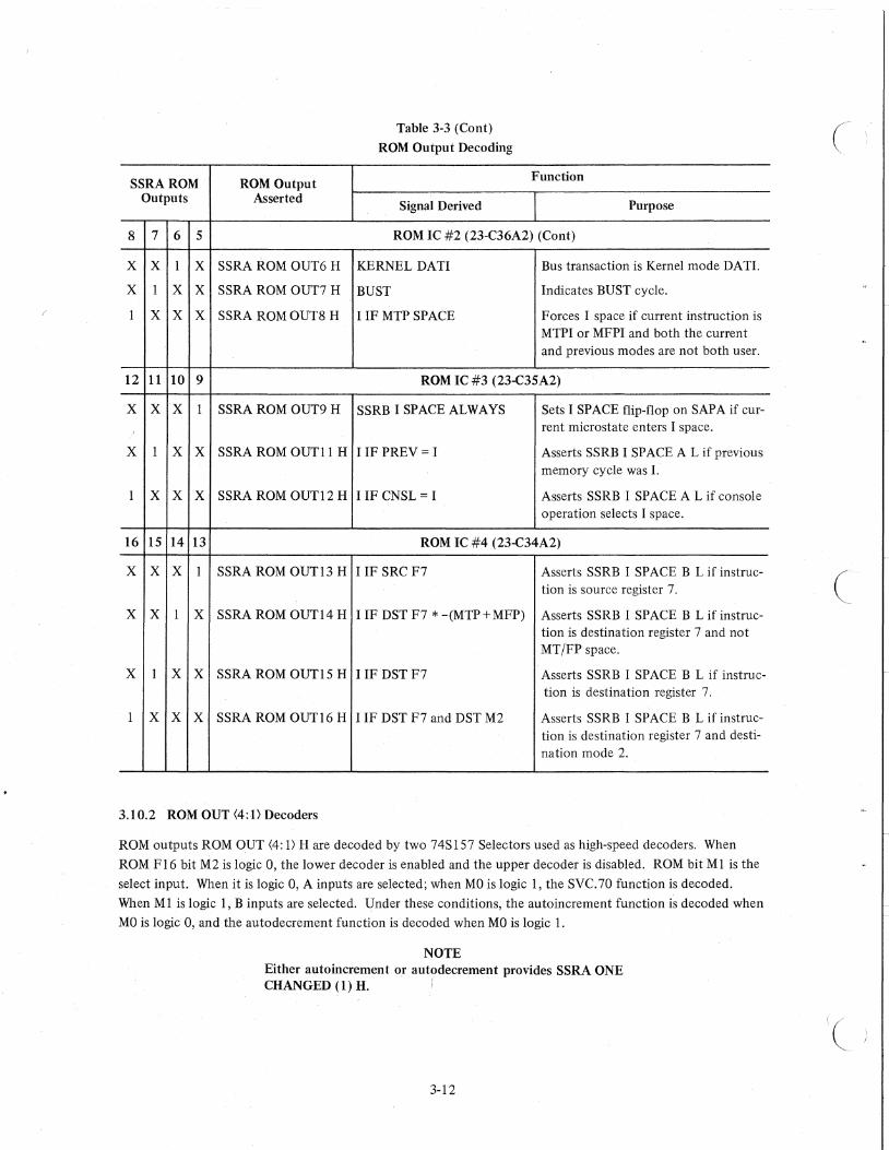
SSRAROM Outputs
8 7 6 5
X X I X
X I X X
1 X X X
12 11 10 9
X X X 1
,
X 1 X X
1 X X X
16 15 14 13
X X X 1
X X I X
X 1 X X
I X X X
ROM Output Asserted
SSRA ROM OUT6 H
SSRA ROM OUT7 H
SSRA ROM OUT8 H
SSRA ROM OUT9 H
SSRA ROM OUT 1 1 H
SSRA ROM OUTI2 H
SSRA ROM OUT13 H
SSRA ROM OUTI4 H
SSRA ROM OUTI5 H
SSRA ROM OUTl6 H
Table 3-3 (Cont)
ROM Output Decoding
Signal Derived
Function
Purpose
ROM IC #2 (23-C36A2) (Cont)
KERNEL DATI Bus transaction is Kernel mode DATI.
BUST Indicates BUST cycle.
I IF MTP SPACE Forces I space if current instruction is MTPI or MFPI and both the current and previous modes are not both user.
ROM IC #3 (23-C35A2)
SSRB I SPACE ALWAYS Sets I SPACE flip-flop on SAP A if cur-rent microstate enters I space.
I IF PREV= I Asserts SSRB I SPACE A L if previous memory cycle was I.
IIF CNSL = I Asserts SSRB I SPACE A L if console operation selects I space.
ROM IC #4 (23-C34A2)
I IF SRC F7 Asserts SSRB I SPACE B L if instruc-tion is source register 7.
I IF DST F7 * -(MTP + MFP) Asserts SSRB I SPACE B L if instruc-tion is destination register 7 and not MT/FP space.
I IF DST F7 Asserts SSRB I SPACE B L if instruc-tion is destination register 7.
I IF DST F7 and DST M2 Asserts SSRB I SPACE B L if instruc-tion is destination register 7 and desti-nation mode 2.
3.10.2 ROM OUT (4:1> Decoders
ROM outputs ROM OUT (4: 1> H are decoded by two 74S 157 Selectors used as high-speed decoders. When
ROM Fl6 bit M2 is logic 0, the lower decoder is enabled and the upper decoder is disabled. ROM bit MI is the
select input. When it is logic 0, A inputs are selected; when MO is logic I, the SVC.70 function is decoded.
When M 1 is logic 1, B inputs are selected. l!nder these conditions, the autoincrement function is decoded when
MO is logic 0, and the auto decrement function is decoded when MO is logic 1.
NOTE Either autoincrement or auto decrement provides SSRA ONE CHANGED (1) H. :
3-12
(
c-
(
c
When ROM bit M2 is logic 1, the upper decoder is enabled and the lower decoder is disabled. M 1 is the select in
put. When Ml is logic 0, A inputs are selected. Under these conditions, the BRK.30 (instruction complete)
function is decoded when MO is logic 0; when MO is logic 1, the JSR.30 function is decoded. When Ml is logic 1,
the decoder outputs are irrelevant.
The truth table for the ROM outputs is shown on drawing SSRA. The outputs are clocked into the 74175 flip
flops by SSRK P~LSE 23 H, which occurs near the beginning of every processor microcycle (Paragraph 3.14).
The following paragraphs describe the functions of microstates decoded from the ROM OUT (4: 1) outputs.
3.10.2.1 RESTORE PS - SSRA RESTORE PS (1) H is asserted only during processor microstate SVC.60. This
is the Bust part of the push of the old PS onto the stack specified by the new PS during any trap or interrupt sequence. SSRA RESTORE PS (1) H is inverted and renamed SSRA SET PSR L. This output sets the PSR flip
flop at SVC.60. The PSR flip-flop remains set until SSRA CLR PSR (1) H is asserted, which occurs during the
FET.OO or BRK.OO microstates. Thus, the PSR flip-flop is only set during the push of the old PS and PC onto
the stack during a trap or interrupt. If a KT ll-C abort occurs during either of these push attempts, the old PS
and PC must be restored. The old PS is temporarily stored in the processor BR; the old PC is temporarily stored
in the processor DR.
The purpose of SSRA PS RESTORE (1) H is to force the processor through microstates ZAP.l 0 through ZAP.30
and to enable clocking of the PS register in the processor. Refer to Flow Diagram 12 in the KBII-A drawing set.
The old PS is restored to the PS register, and the old PC is restored to the PC register. PS RESTORE allows pro
per recovery from aborts on interrupt and trap sequences.
3.10.2.2 SSRA JSR.30 (ROM (3:1) = 5) - If an abort occurs during a JSR instruction, SSRA JSR.30 (1) H as
serts SSRA INH PWE H (Inhibit Pad Write Enable), which prevents the processor from writing into the general
registers. This function may be invoked if an abort occurs on the push of the destination register onto the stack
during a JSR (microstate JSR.30) or if an abort occurs on the fetch of the new top of the stack (MRK.20).
At JSR.30 the old PC is normally written into the destination register thus destroying the destination register
contents. SSRA INH PWE prevents. this destruction. At MRK.20 the stack pointer, register 6, is normally modi
fied by N (the MARK argument) + 2. SSRA INH PWE prevents this modification if an abort occurs at the new
top of the stack. Signal SSRA JSR.30 allows proper recovery from aborts at JSR.30 and MRK.20 microstates.
3.10.2.3 BRK.30 (ROM (3:1) = 4) - The BRK.30 microstate is decoded from the ROM as an indication that
the current instruction is complete and that some interrupt or trap memory reference is about to begin. BRK.30
(1) His ANDed with SSRC NO ERROR H to set the INSTR COMP flip-flop (drawing SSRE).
3.10.2.4 AUTO DEC (ROM (3:0 = 3) - The AUTO DEC signal is decoded from the KTlI-C ROM for any
microstate in which auto decrementing a general register is required. The AUTO DEC signal controls the MSB of
each SRI byte and configures the 2's complement generator (Paragraph 3.12).
3.10.2.5 ONE CHANGED (ROM (3:I> = 2 or 3) - The ONE CHANGED flip-flop is set when any microstates in
which autoincrement or auto decrement occurs is decoded from the KTlI-C ROM. This flip-flop sets the ONE
AUTOED flip-flop (Paragraph 3.12) for the purpose of clocking byte 0 and byte 1 of SRI. It is initially cleared
so that the first general register that is "autoed" is described in byte 0 of SRI. ONE AUTOED is then set. If a
second general register is autoed during the instruction, that general register description is loaded into byte 1 of
SRI.
3-13

3.10.2.6 DST - ROM OUT 4 H indicates destination mode. When the current memory reference is the final
reference of a destination calculation, ROM OUT 4 H is asserted. The microstates that provide ROM OUT 4 are
listed on SSRB. The ROM OUT 4 H output controls the state of the DST flip-flop, which is clocked by TIGC
TI L. This provides the "maintenance" facility that is used by certain memory diagnostic programs; it is not to
be used for any other purpose.
3.10.3 Kernel Space Control
Refer to drawing SSRB. Four conditions select the KERNEL SPACE flip-flop:
a. By doing an EXAM or DEP operation under consok control.
b. By SSRA ROM OUT6 H, indicating the Kernel DATI bus condition (trap, interrupt, or abort).
c. By BSOPI bus condition (SSRA ROM OUTS H) if the instruction is a move to or from previous data space, and the previous processor mode was Kernel.
d. If current processor mode is Kernel, the console is not active, and the instruction is not a BSOPI transaction and not a move to or from previous data space.
Any of the above conditions qualifies the D input of the KERNEL SPACE flip-flop. It is clocked and reset to
assert SSRB KERNEL SPACE (1) L at Tl of the Bust cycle.
3.10.4 Supervisor Space Control
Refer to drawing SSRB. The three conditions that select the SUPER SPACE flip-flop are similar to those that
select KERNEL SPACE (Paragraph 3.10.3, a, c, and d). The SUPER SPACE flip-flop is qualified if:
a. Selected by doing an EXAM or DEP operation under console control.
b. Selected by BSOPI bus condition if instruction is a move to or from previous data space, and the previous processor mode was Supervisor.
c. Selected if current processor mode is Supervisor, the console is not active, and the current instruction is not a BSOPI transaction and not a move to or from previous data space, and not a Kernel DATI.
When any of these conditions are true, the SUPER SPACE flip-flop asserts SSRB SUPER SPACE (1) L.
3.10.5 User Space Control
The only differences between User space control conditions and Supervisor space control are the processor status
word bits and console control switch selections. Thus, the USER SPACE flip-flop is qualified if:
a. Selected by doing an EXAM or DEP operation under console control.
b. Selected by BSOPI bus condition if instruction is a move to or from previous data space, and the previous processor mode was User.
c. Selected if current processor mode is User, the console is not active, and the current instruction is not a BSOPI and not a move to or from previous data space, and not a Kernel mode DATI.
3.10.6 I Space Control
Refer to drawing SSRB. The I space decoders assert I SPACE A L or I SPACE BLunder the following conditions:
a. SSRA ROM OUT8 H. I space is selected if the current instruction is a move to or from previous I space. IRCA IR 15 (1) L ensures D space (MTPD + MFPD).
(continued on next page)
3-14
(
(

(
c
b. SSRA ROM OUT9 H. This ROM output is an unqualified request for I space. No other conditions are required to assert I SPACE A L. Used for instruction fetches.
c. SSRA ROM OUTll H. This output asserts I space if previous memory reference was I space. It is ANDed with the output of the PREV = 1 flip-flop, which stores the I space condition from the previous memory cycle. Used for continuation of DA TIP bus cycles.
d. SSRA ROM OUT 1 2 H. This output asserts I space if I space is selected at the console control (SAPP CNSL I SPACE H asserted).
e. SSRA ROM OUTl3 H. This output asserts I space if the current instruction is source register 7 (DPCH SRC F7 L asserted).
f.
g.
h.
SSRA ROM OUTl4 H. This output asserts I space if the current instruction is destination register 7 (SSRB DST F7 H), and if the instruction is not an MTP or MFP instruction.
SSRA ROM OUTl5 H. This output asserts SSRB I SPACE A L whenever the destination register is 7.
SSRA ROM OUTl6 H. This output asserts SSRB I SPACE A L whenever the destination mode is 2 and the destination register is 7. It is used only for the special Floating Point immediate construction.
The I space control logic (drawing SSRB) is required to provide high-speed memory management throughput be
cause there is a lack of direct association of I space for each specific microstate. SSRB I SPACEA Land SSRB
I SP ACEB L are used to set the I SPACEA and I SP ACEB flip-flops (drawing SAP A) during Tl of the Bust cycle.
This logic minimizes the delay required to generate the most significant PAR/PDR address bit, which determines
whether an I space or D space PAR/PDR set is addressed.
3.11 STATUS REGISTER 0 (SRO)
The contents and format of SRO are described in Paragraph 2.3.1. The SRO bits and control logic are shown on
drawings SSRC, SSRD, and SSRE. The SRO format is shown in Figure 2-10.
3.11.1 Abort Flags SRO (15:13}
Refer to drawings SAPL and SSRC. SRO bits 15, 14, and 13 are the memory management abort flags that indi
cate the cause of an abort. The fault detection logic is described in Paragraph 3.5 and shown on drawing SAPL.
The fault signal outputs are SAPL NON RES FAULT H, SAPL PGE LENGTH FAULT H, and SAPL READ
ONLY FAULT H. These inputs are applied to a 74157 Multiplexer at the B inputs. If not writing into the SRO,
these inputs are selected as the data inputs to the 74175 flip-flops that store SRO bits (15: 13}.
SSRE STROBE OK L asserts SSRC STROBE ENABLE H when the following conditions are met:
a. Not a BEND (processor will not complete memory cycle). b. No errors have been detected on previous memory references. c. The current memory reference is not accessing an internal register. d. KTII-C is enabled.
SSRE STROBE ENABLE H allows the fault information to be strobed into SRO by the SSRK PULSE. BC89 H
clock pulse that occurs during the processor Pause cycle. The contents of SRO (15: 13} are ORed to the data in
put of the NO ERROR flip-flop, which is clocked by the SSRK PULSE BC91 0 L clock pulse. If no error flags
are set, the NO ERROR flip-flop will remain set.
Data can be written into SRO bits (15: 13} under program control. Buffer register bits PDRB BR (15: 13} BLare
applied to the A inputs of the 74157. When SSRL WRITE SRO REG H is asserted(Paragraph 3.5.1) and SAPH
VA (02: OJ} B L indicate the SRO address, the A inputs are selected as the data inputs to the SRO flip-flops. The
3-15

data will be written into the SRO when SSRK PULSE BC89 H occurs. In this case, SSRC STROBE ENABLE H
is asserted by SSRE WRITE SRO Hand UBCC HI BYTE H.
NOTE Setting the SRO error flags under program control does not cause an abort.
The ABT FLG flip-flop (drawing SSRC) will only be set when the SAPL ABORT COND H signal is asserted and
no internal register accesses are in progress. The state of SRO bits 15, 14, 13 has no effect on the ABORT FLAG.
Figure 3-4 is a simplified diagram that depicts the KTll-C logic and how it interacts with the KB ll-A logic to
force a trap to Kernel D space location 250 when an abort condition is detected. The signal mnemonic prefixes
indicate where each signal is generated in the two units. Refer to the KB l1-A drawings for more complete details.
3.11.2 Memory Management Trap (SRO Bit 12)
The memory management trap control logic is shown on drawing SSRD. The decode logic that detects trap con
ditions is shown on drawing SAPL and described in Paragraph 3.6.4. Figure 3-5 is a simplified diagram that shows
the KTlI-C trap control logic and the interaction with the KB Il-A trap control logic.
3.11.2.1 Enable Management Traps - The ENABLE MGMT flip-flop (SRO bit 09) must be set by program con
trol. This is accomplished by writing into the SRO with data bit BR09 on a logic 1. The SSRD DATA 09 H in
put is clocked into the ENABLE MGMT flip-flop by SSRE SRO HIB CLK L, which is produced when T3 occurs
during the Pause cycle.
Several other conditions must be satisfied before a memory management trap can occur. These are:
a. SSRE RELOC H must be asserted, indicating the KTlI-C is enabled. b. The bus transaction has not been terminated by Bus End (BEND). c. No internal register is being accessed. d. No abort occured during the memory access.
3.11.2.2 Pre-Management Trap - If the conditions specified in 3.11.2.1 are satisfied and one of the three mem
ory management trap conditions is decoded (Paragraph 3.6.4), SSRD PRE MGMT TRAP H is asserted. Because
the MEM MGMT TRAP DETECTED flip-flop is initially cleared, the MGT TP DET DLY L signal is high at this
time. As a result, SSRD CUR FL T L causes SSRD MEM MGMT TRAP L to be asserted. This is the trap signal
that is sent to the processor. The same conditions that caused SSRD MEM MGMT TRAP L to be asserted allow
the MEM MGMT TRAP DETECTED flip-flop to be direct-set when clock pulse SSRK PULSE BC89 H occurs.
SSRD PRE MGMT TRAP H guarantees that a trap will be executed on the last memory reference of an instruc
tion, before the next instruction is started.
3.11.2.3 Memory Management Hold - When SSRK PULSE BC89 H occurs, SSRD MEM MGMT B H is asserted.
SSRD MGT TP DET DL Y L will remain high for 50 ns. Thus, a 50-ns SSRD SET MGMT HOLD L pulse is pro
duced to direct-set the MEM MGMT HOLD flip-flop. The purpose is to maintain the SSRD MEM MGMT TRAP L
signal to the processor until it is acknowledged. Because traps are not handled by the processor until the end of
an instruction, several memory references may occur before the processor sends TMCA SEG ACKN L, which
clears MEM MGMT HOLD. Once the MEM MGMT TRAP DETECTED flip-flop (SRO bit 12) is set, it will not
cause another trap until it is cleared, even though additional trap conditions may be detected. It is normally
cleared under program control by writing a 0 into bit 12 of SRO.
3-16
c
(
(
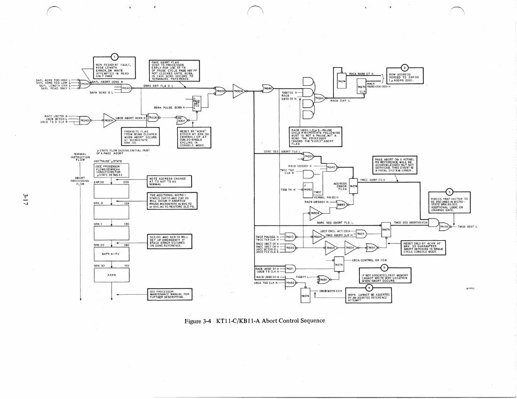
W I
-l
('
SAPL ADRS TOO HIGH L
PAGE ABORT FLAG SENT TO PROCESSOR EARLY FOR USE AT T2 OF PAUSE eye LE PAGE ABT FF NOT cLOCKED UNTIL Be89, IN CASE BEND OCCURS TO TERMINATE REFERENCE
S~kptD~~N~~~ ~~~ t ;'),._~S:::SR:!!G~AB~T'-!:.FL:;:G:...:::D..:L'-_-"-_____ ~,~"6i SAPL REAO ONLY L
RAce ueCT01 H-,----.... ueeB eCToa L
ueeB TS 3 elK H
NORMAL INSTRUCTION
FLOW
I ABORT
PROCESSING FLOW
P. STATE FLOW DURING INITIAL PART OF A PAGE ABORT
NOTE ADDRESS CHANGE AT T2 NOT T3 AS NORMAL
THE ADDITIONAL MICRO
~:-::--T--:==-=~----ll STATES ZAP.10 AND ZAP. 20
n, ~~h~~~~g:O~T:~~~;~~C,70 or SVC.90 TO RESTORE OLD PS.
SER.OO AND SER.10 WILL SET UP EMERGENCY IF STACK ERROR OCCURED ON SAME REFERENCE,
{\
SSRC SEG
TMCE PAUSES H TMCC T53 elK H
RACC USCT 01 H RACC USCT 02 H UBCC BCTOO B L UBCe TS3 CLK 4
RAce UBSD 01 H UBCB T3 CLK H
RAce UBSD 01 H
UBCA TS2 CLK H
TlGBTS2 H RAce ueSD 01 H 74SS4)o)c_..L..-----..J
~8~E yt~Pc:~b2srA~E PtdLI~W'NG BUST IS NOT A PAUSE.8UT A BEND THE PROCESSOR lGNORS THE "EARLyM ABORT FLAG
Figure 3-4 KT11-C/KB ll-A Abort Control Sequence
,/""\ \
TMCB SEOT L

If -00
('
ACF=I :TRAPON READ ACF=5~TRAPON WRITE ACF =4: TRAP ON READ
OR WRITE
SSRC PAGE ABORT FLG (OJ H
~
ASSERTED I F TRAP CONDITION DETECTED, NOT INT REG. ACCESS,NOT A PROCESSOR BEND
SSRD PRE MGMT TRAP H
PRDGR·AM CONTRDll.ED TO ENABLE MEM.MGMT TRAPS WHEN SET
HOLD IS SET BY lEADING EDGE OF SRO BIT 12.THIS AllOWS PROCESSOR TO SERVICE. TRAP, RESETTING BIT 12 lATER. WILL NOT BE SET·BY WRITING SRO BIT 12= I FROM PROGRAM.
M
3tOtA
w
74S74
PROCESSOR REQUIRES TRAP SIGNAL BY TS3 OF PAUSE CYCLE, KTl1-C MEM.MGMT. SENDS"EARLY" TRAP. IF PAUSE FOllOWS BUST, TRAP OCCURS AT TS3.IF BEND FOLLOWS BUST, PROCESSOR IGNORES TRAP SIGNAL
TMCA SEGT F L
FEEO·BACK PATH TO RETAIN TRAP FLAG UNTIL PROCESSED
SSRD MGMT 74S74 J--l HOLD (i) L
TMCE BRQ ~OBE H ~ TMCE BRQ
T~~G~ ---v-~ elK H
SAPO ATTN {I)H
Figure 3-5 KTlI-C/KB ll-A Trap Control Sequence
(~
NOTE:
OUR I NG INT PROCESSING OCCURS DURING PAUSE MICRO STATES. AT OTHER TIMES DURING NON-PAUSE MICRO STATES
FORCES TRAP SEQUENCE TO VECTOR TO KERNEL VIRTUAL ADDR·ESS 250
Numbered tu! bOlles indicote lime sequence
-!
o
c
l
3.11.2.4 Writing Into SRO Bit 12 - The MEM MGMT TRAP DETECTED flip-flop can be set or cleared under program control by writing into the SRO with data bit SR 12 on a 1 or O. SSRD DATA 12 H is clocked into the flip-flop by SSRD SRO HIB CLK L. Because SSRD PRE MGMT TRAP Hand SSRD MEM MGMT BLare not asserted, no memory management trap will occur.
3.11.3 Trap Flag (SRO Bit 11)
The TRAP flip-flop (SRO bit 11) is shown on drawing SSRD. The flip-flop is direct-set by the TRAP L input. The MEM MGMT HOLD flip-flop is set by the positive-going edge of the TRAP L signal. As a result, the SSRD MEM MGMT TRAP L signal is sent to the processor. The memory management trap service routine must interrogate the SRO to determine whether the trap was caused by an access code violation detected by the KTII-C or by the trap flag.
The flag can be set or cleared under program control by writing into the SRO with data bit BRII set to I or O. Setting the TRAP flip-flop under program control does not cause a memory management trap.
3.11.4 DST MODE (SRO Bit 08)
Refer to the mode/status control logic shown on drawing SSRE. The DST MODE flip-flop (SRO bit 08) is set or cleared under program control by writing into the SRO with data bit BR08 set to I or O. The data is clocked into the DST MODE flip-flop by SSRE SRO HIB CLK L. This bit is set by program control during maintenance operations, which are performed with the RELOCATING flip-flop (SRO bit 00) cleared. When the DST MODE flipflop is set, the true output is ANDed with SSRA DST (1) H to assert the SSRE RELOC H signal. SSRA DST (1) H is decoded from the ROM when the final destination address is calculated. The purpose of this logic is to assert SSRE RELOC H only when the final address is calculated; thus, in the maintenance mode, only the final address is relocated and protected by the KT II-C unit.
NOTE SRO bit 08 is used by the KT11-C diagnostic programs and is . not to be used for any other purpose.
3.11.5 INSTR COMP (SRO Bit 07)
Refer to drawing SSRE, which shows the INSTR COMP flip-flop, SRO bit 07. This bit indicates the status of ellch instruction. It is cleared at the beginning of each new instruction if the preceding instruction was executed without a page error. When the BRK.30 microstate is decoded at the ROM output, the INSTR COMP flip-flop is again set. Reaching the BRK.30 microstate implies that an,interrupt is in progress and that the next memory reference will not be caused by an instruction. Setting the INSTR COMP bit in the SRO provides the error handling routines with a means of determining whether the current instruction needs to be repeated in the course of recovering from an abort or whether some interrupt sequence will have to be emulated.
3.11.6 SRO Mode Field (SRO Bits (06:05»
The SRO mode field (bits 06 and 05) is shown on drawing SSRE. These bits are determined by the SSRB SRO MODE (1 :0) H D inputs to the 74175. The truth table for these inputs is:
SSRB SRO Mode Space Mode Asserted SRO Mode Field
1 0
SSRB KERNEL SPACE (1) L H H 00 SSRB SUPER SPACE (I) L H L 01
-SSRB USER SPACE (1) L L L II None (Illegal) L H 10
3-19
SRO mode field lOis illegal. _ Any attempt to access memory in that mode is aborted. Because no space is,
selected, the outputs of all PAR/PDRs are high. The ACF is therefore 111 (key = 7), an abort condition.
The SROmode field bits are clocked into the SRO at the end of the Pause cycle by SSRK PULSE BC89 H if
SSRE STROBE OK His asserted. This only happens when:
a. KT ll:.c is enabled.
b. No BEND is issued by the processor.
c. No internal register is involved.
d. No paging error was detected on a previous bus cycle. If an error was detected, the mode field associated with the previous memory reference must be retained in SRO (06:05) to aid in error recovery.
3.11.7 Address Space -:- lID (SRO Bit 04)
Refer to drawin~ SSRE. SRO bit 04 indicates whether I or D space is being addressed. The bit is stored by one
D-type flip-flop of a 74175. If I space is not addressed, SAPA IND DATA H is high at the input, and SRO bit 04
will be set when clocked, indicating Dspace is addressed. The bit is clocked under the same conditions as de,
scribed in Paragraph 3.11.6.
3.11.8 Page Number (SRO Bits (03:0t»
Refer to drawing SSRE. SRO bits (03:01) are stored by three D-type flip-flops. The inputs are SAPH VA
<IS: 13) H, which represent the page number being addressed. These bits are clocked as described in Paragraph 3;11.6.
3.11.9 KTll-C RELOCATING (SWO Bit 00)
Refer to drawing SSRE. The KTlI-C RELOCATING flip-flop (SRO bit 00) is orily set under program control by
writing into the SRO with data bit BROO set to 1. Normally, setting SRObit 00 will assert SSRE RELOC H. The
only exception is when performing a physical memory access from the console. Then, SSRA KY PH MEM AC
(0) H goes low and inhibits SSRE RELOC H. This allows the address set on the console switches to address the
physical unrelocated address.
NOTE This bit essentially turns the KT11-C on and off.
3;12 STATUS REGISTER. 1(SR1)
Refer to drawingSSRF. Status Register 1 is a 16-bit register comprising four 74S174 D-type flip-flops. (Two
flip-flops on each 74S174 are not used.) SRI keeps track of any autoincrementing or auto decrementing of the general registers that may occur during the execution of instructions. The layout of SRI is shown in Figure 2-12.
When a general register is either incremented or decremented, the general register address GRAC GRA (2:0> B H
and the number of bits by which the register was modified are stored in SRI. SRI is divided into bytes 0 and 1.
The low order byte (byte 0) is written first. SRI is a read-only register; it cannot be written into under program
control.
3.12.1 General Register Address
The general register address is available on inputs GRAC GRA (2:0) and is applied to the three low order bits of
each byte in SRI. When the general register destination is in Register Set 1, GRAC GRA3 L is asserted and
3-20
(
(

(
SSRF GRA3 B H goes high. The purpose of this logic is to inhibit SSRF GRAO B H if general register 17 (User
mode Stack Pointer) is addressed. Thus, a reference to GRA17 is stored in Status Register 1, Register Number field as R6.
3.12.2 Autoincrement/ Autodecrement
The constant that indicates the number of bits by which the general register was modified is available on inputs
DAPD KOMX (03:00> B L. The KOMX constant multiplexer provides only constants 1,2,4, or 8; thus, only one
of these inverted inputs will be logic 0 for any of these four constants. When the general register is decremented
by a constant, the processor "subtracts" a positive constant. Therefore, the 2's complement of the constant is
generated by the KT11-C logic. The 74S157 Multiplexer is used as a 2's complement generator for this purpose;
the 74S157 is always enabled. During a decrement operation, SSRA AUTO DEC (0) H is low and the A inputs
are selected to provide the 2's complement of the constant. During an increment, SSRA AUTO DEC (0) H is
hig.'1 and the B inputs are selected to provide the constant as a positive binary number. Table 3-4 shows the con
stant multiplexer truth table for both decrement and increment outputs. The constant is input to bits SRI
(06:03) of byte 0 or SRI (14: 11) of byte I. The SSRE AUTO DEC (1) H signal is input to SRI as the MSB of
each byte. This bit functions as a sign bit for each byte, indicating a decrement or an increment operation.
Table 3-4
Truth Table for Constant Multiplexer Outputs
DAPDKOMXBL SSRA AUTO DEC (1) H SSRA AUTO DEC (0) H Constant
03 02 01 00 02 03 01 + 00 00 03 02 01 00
1 1 1 1 0 1 1 I 1 0 0 0 1 2 1 1 0 I 1 1 1 0 0 0 1 0 4 1 0 1 1 I 1 0 0 0 1 0 0 8 0 1 1 1 1 0 0 0 1 0 0 0
3.12.3 Examples of SRI Loading
As an example of SRI loading, assume general register R5 is autoincremented by 2 in the source calculation of
an instruction. SRI is initially cleared by SSRH LOAD IR L. The ONE AUTOED flip-flop is also cleared. The
general register R5 address is availa1:>le at the GRAC GRA (2:0) inputs. The constant 2 is provided by DAPD
KOMX 01 B L, and because the calculation is an increment, the 2's complement of the constant is selected.
Therefore, the information that is clocked into byte 0 of SRI at time T5 is shown in Figure 3-6a. Further as
sume that general register R4 is autoincremented by 4 in the destination calculation of the instruction. The
ONE AUTOED flip-flop is set when clock pulse SSRK PULSE 51 H occurs to provide SSRF CLK BYTE 1 H.
Byte 1 of SRI will be loaded as shown in Figure 3-6b at that time.
If an error occurs between the time one instruction is loaded (RACA UIRK H) and the time the next instruction
is loaded or an interrupt is processed (BRK.30), SRI has the general register modification information required
to recover from the error. This information is available to the software recovery service routine.
Once the instruction is complete, no error has been detected, and an interrupt is being serviced, SSRA BRK.30 L
and SSRC NO ERROR (1) H clear SRI and the ONE AUTOED flip-flop. Any stack modification that occurs
from that point until the next instruction fetch is recorded. There will be no need to restart the instruction,
even if segmentation faults are detected before the next instruction fetch. Instead, the trap sequence has to be
emulated to completion to recover and restart.
3-21

1\
BYTE 0 0"1
15 8 3 I 2
SRI 11 o II 0 1 I I -2 I R5 I
o. AUTO-DECREMENT R5 BY 2, SOURCE CALCULATION
1'15 BYTE 1
8 "17 11 110 3 I 2 o I SRl I 0
0 0 o 11 0 Oil o II '0 I I +4 I R4 I -2 I R5 I
b. AUTO- INCREMENT R4 BY 4, DESTINATION CALCULATION
11- 1035
Figure 3·6 Examples of SRI Loading
3.13 STATUS REGISTER 2 (SR2)
SR2 consists of three 74174 D-type flip-flops (drawing SSRFl). Itis loaded with the l6-bit virtual address SAPH
VA <15: 00> B H at the start of each instruction fetch. Under these conditions, it stores .the virtual address of
each current instruction. It can also be loaded with the trap vector at the beginning of an interrupt or "T" bit, Parity, Odd Address, and Timeout traps. The clock input, SSRH NEW SEQUENCE CLK H, is produced by
RACA DIRK H or the BRK.30 (0) L signal decoded at the KT1l-C ROM output.
NOTE SR2 is read only; it cannot be written into.
3.14 INTERNAL DATA BUS MULTIPLEXERS
The internal data bus multiplexers are made up of eight 74153 Multiplexers, Shown on drawing SSRJ. The multi
plexers are capable of selecting the contents of one of four registers as the l6-bit output to the processor internal
data bus. The inputs are the APR, SRO, SRI, or SR2. The APR can be either the PAR or the PDR, depending
upon the input selected by the PAR/PDR read multiplexer (Paragraph 3.7).
The specific register selected is detetmihed by decoding virtual address bitsBAMX (02:01); the SSR REG flip
flop, and SSRL APR REG L. The input selection logic decodes this information as indicated in the following
chart:
SSRHBAMX Input Function Selected As SSRL SSR REG (I)H SSRLAPRREG
Internal Data Bus Output 02 01 SI SO
0 1 1 0 0 0 A: SRO <15:00> H 1 0 1 0 0 1 B: SRI <15:00) H 1 1 1 0 1 0 C: SR2 <15:00) H
* * 0 1 1 1 D: APR <15:00) H
1 indicates assertion, 0 indicates non-assertion, * indicates irrelevant.
3-22
(
c--

c
l
The multiplexers are enabled when T~CE C I H is asserted by the processor, provided that an internai register is
addressed and the TMCF GET OFF II input is not asserted. At this time, data in the addressed register is avail
able on the processor internal data bus lines, INT BUS DATA (15:00) H. The TMCF GET OFF input is only as
serted for floating-point processor or switch register operations that use the same processor internal data bus lines.
3.15 KTII-C MEMORY MANAGEMENT TIMING
Timing for the KT1I-C option is derived from KBII-A Central Processor time states TlGD TS (5:2) H (drawing
SSRK). The processor time state inputs are not fixed but vary in length depending on the type of cycle through
which the processor is progressing. Sample timing for the Bust and Pause memory cycles is shown in Figure 3-7.
Note the memory management delay indicated on the diagram. The TlG module is normally jumpered to pro
vide three time periods of delay. This is adequate for the KTlI-C logic to complete its functions and allow the
processor to continue through the Bust cycle.
3.15.1 Event Times Related to Memory Cycles
Table 3-5 is a chart that shows how the KTlI-C events relate to the KBII-A memory cycles and time states. The
heavy lines indicate that an event occurs over an extended period of time. For example, the INT REG flip-flop
remains cleared over the first half of Tl. An asterisk indicates the possibility of an event if conditions other than
timing are met. For example, if the BRK.30 microstate is decoded or the UIRK field of the current processor
microstate is set to I, SRI will be cleared through the remainder of the memory cycle. The chart includes draw
ing references, indicating where the associated timing logic is on the block schematics.
3.15.2 Address Relocation Timing
Figure 3-8 is a simplified diagram that shows the timing of the events that occur during page address relocation.
The. sequence of events is indicated by the numbered text boxes. Maximum time lapse for an event to occur is
related to the leading edge of processor time state TI.Statements within rectangles apply to address relocation
when the KT ll-C is enabled, and a 16-bit virtual address is converted to an 18-bit physical address. Statements
within ovals apply when the KTlI-C is disabled (SRO bit 00 = 0), and the 16-bit virtual address is passed through
the KTlI-C without change.
3.15.3 Internal Register Access Timing
Figure 3-9 is a simplified diagram that shows the sequence of operations involved in a typical internal register ac
cess. The specific conditions assumed for this example are stated in the notes. Note that as SOon as the KPAR
contents are added to the virtual address arid the resultant UPAR physical address is decoded, theD input of the
User PAR flip-flop goes high. It is clocked at T5 of the Bust cycle, and.SSRL INT REG FAST L is asserted.
That signal de-selects the KPAR as shown. It is also sent to the processor in acknowledgement of a Fastbus ad
dress. All the KT Il-C internal registers are Fastbus device addresses .. Therefore, the KB Il-A proceeds through
a Fastbus memory cycle, not a Unibus cycle.
For a read (DATI) operation, the contents of the selected UPAR will be gated to the processor internal data bus
(statements 8R and 9Ron Figure 3-9). For a write (DATO) operation, the data from the processor BR will be written into the selected UPAR at T4 of the Pause cycle (statements 8W and 9W on Figure 3-9).
3.16 INTERNAL REGISTER CONTROL
The internal register address decode and control logic is shown on drawing SSRL.
3-23
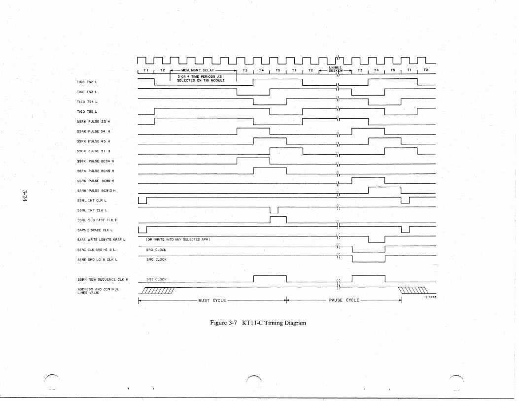
w N .j:>.
(~
TIGD TS2 L
TIGO- TS3 L
TIGD TS4 L
TIGD TS5 L
SSRK PULSE 23 H
SSRK PULSE 34 H
SSRK PULSE 45 H
SSRK PULSE 51
SSRK PULSE BC34 H
SSRK PULSE BC45 H
SSRK PULSE BCS9 H
SSRK PULSE SC91D H
SSRL INT CLR L
SSRL INT CLK L
SSRL SEG FAST CLK H
SAPA I SPACE elK L
SAPA WRITE LOBYTE KPAR L
SSRC eLK SRO HI B L
SSRE SRO LO B elK L
SSRH NEW SEQUENCE elK H
ADDRESS AND CONTROL LINES VALID
UNIBUS I T 1 I T2 Pi. MEM. MGMT. DELAY 'I n T4 T5 T1 T2 r--: DES~fW:=1 n T4 T5 T1 I T2
30R 4 TIME PERIODS AS j) ~. . SELECTED ON TlG MODULE L-___________ -=~~--~~~I~,.~~~
'1\-I' ~j r--
....(, ~ r----"
r---==::::;------l\~ H 11
~ __ ~II L-- IJ
~~~~----~\\~--------------
----~------------~ ~----~\\
--------------------------~--~\~ ~----------------------------~~~ I ,--I ____ _ U U
II U ---- -J)
____________________________ ~r__l \~
U II U ------------------------------------~" r----------(OR WRITE !NTO ANY SELECTED APR) J J L---.J
SRO CLOCK I~ SRO CLOCK \ ~~----------:----------------
SR2 CLOCK \~--- 1'--______ __
III/I/l! II \ \ \\\\\\\\\ I' BUST CYCLE + PAUSE CYCLE ,I 11-0778
Figure 3-7 KTlI-C Timing Diagram
/~ .~
.------------~-----------------------------------------------~----------------------,---------------------------------------------------------------------------

W I
N VI
(' ~,
Table 3-5
How KTII-C Events Relate to I\B ll-A Memory Cycles
Status Registers
CPU Time SRO SRI SR2 SR3
Cycle State PAR's & POR"s CLR CLK CLR CLK Q.R CLK CLR CLK
Tl
T2 *Clear SRI (SSRF)
BUST BRK.30
T3
T4 ' *Clack SR2 (SSRM)
T5 Clock A and W *Clock FF's (SAPO) SRI
(SSRF)
Tl -
T2 *Clear SRI (SSRF)
PAUSE LDIR
T3 *Clear Clock INST SRO COMP (SSRO) FF (SSRO)
(SSRE) -
T4 *Write Data into *Clock PAR's or POR's. SR2 (SAPA-F) (SSRH)
T5 *Clock *Clock SRI SR3 (SSRF) (SAPN)
(NEXT) Tl
*Indicates possible event; dependent upon conditions other than timing.
" (~
,
Control Logic Timing
I~Iear INT REG (SSRL). Clock I SPACE FF's (SMA). Clock "SPACE" FF's (SSRB). Clock OST and KYPH MEM AC FF's (SSRB).
Clock ROMOUT 3:1 FF's (SSRA).
Clock PREV=I (SSRB).
Clock INT REG AND SEG FAST FF's (SSRL)
Clock ROMOUT 3: 1 FF's (SSRA). Clear "SPACE" FF's (SSRB)*.
Clock NO ERROR (SSRC). ,--- -- --
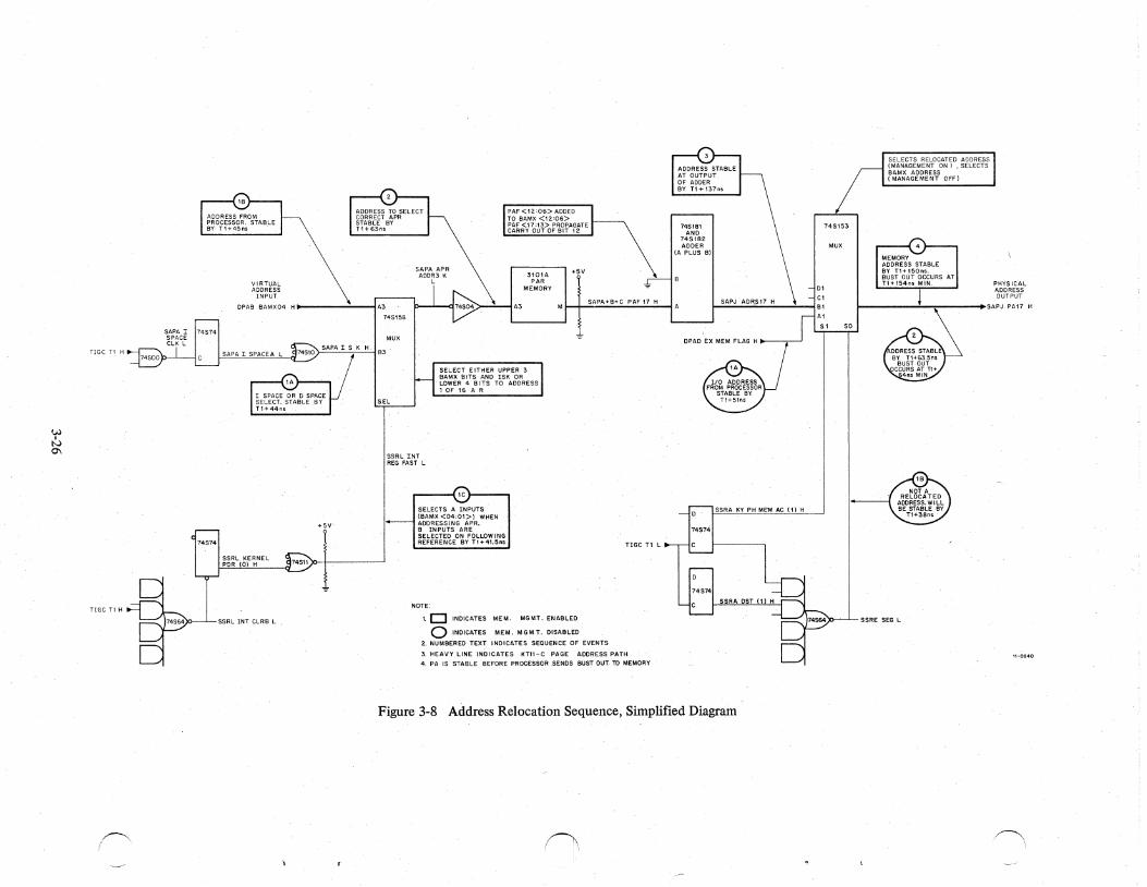
74S74
TIGC Tl H
w N 0\
74S74
TlGC T\ H
(~
VIRTUAL ADDRESS
INPUT
DPAB BAMX04 H ... ----""..--!.
+5V·
SSRL KERNEL ~)O-I PDR (0) H
SSRL INT CLRB L ,
PAF<12:06>' ADDED TO BAMX <12:06> PAF <17:13> PROPAGATE CARRY OUT OF BIT t 2
3101A PAR
MEMORY
+5V
M I I SAPA+B+C PAF \7 H
S~RL INT REG FAST L
SELECTS A INPUTS (BAM·X <04;01> I WHEN ADDRESSING APR~ B INPUTS ARE SELECTED ON FOLLOWING REFERENCE BY 1I+41.5n9
NOTE:
1. 0 INDICATES MEM. MGMT. ENABLED o INDICATES MEM. MGMT. DISABLED
2, NUMBERED TEXT INDICATES SE~UENCE OF EVENTS
TIGC T1 L
3. HEAVY LINE INDICATES KTlI-C PAGE ADDRESS PATH
4. PA IS STABLE BEFORE PROCESSOR SENDS BUST OUT TO MEMORY
745181 AND
745182 ADDER
(A PLUS B)
74574
74574
745153
MUX
01
I 5APJ ADRSI7 H I~!
SSRA KY PH MEM AC (0 H
AI
51 SO -r---r
Figure 3-8 Address Relocation Sequence, Simplified Diagram
0,
SELECTS RELOCATED ADDRESS (MANAGEMENT ON) . SELECTS BAMX ADDRESS (MANAGEMENT OFF)
MEMORY ADDRESS STABLE BY T1+ 150ns. BUST OUT OCCURS AT T1+154ns MIN. PHYSICAL
ADDRESS OUTPUT
t-----...:.-,r---•• SAPJ PA17 H
SSRE SEG L
o

w , IV -.J
(' I
SSRB KERNEL SPACE (1) L
74574
KERNEL PAR IS DE-SELECTED . AT T2 OF PAUSE CYCLE BY SSRL INT REG FAST
SSRK PULSE 23 H'
SSRA RQMOUT 1 H
( BUST)
CLR
SAPA ADOR<2:0> H
745181 "LU
" PLUS 8
BAMX <15:13> 'ADDRESS t OF 8 KPAR'S TO PROVIDE PAGE BASE ADDRESS
74504
~
SAPA+8+C PAF<t7,06>H
SSRA ROM OUT 7 H
TIGC n H
RESET AT BEGINNING OF NEXT MEMORY REFERENCE. NORMAL MEM. CYCLE OCCURS
SSRL USER PAR (0 L
~I:> 00';.. " .. """ C"o. • 0(745151'>------,-----------'
SSRL INT REG FAST CAUSES BAM X <03:01 > TO 'BE SELECTED AS ADDRESS INPUTS
Figure 3-9 Internal Register Access Sequence, Simplified Diagram
SAPA+B+C PAF < 17 :06> H
NOTES:
1. NUMBERED TEXT BOXES INDICATE TIME SEQUENCE OF OPERATIONS
2. SPECIFIC CONDITIONS ARE; A. PROCESSOR IN KERNEL MODE B. KTl1-C ENABLE
(\
C, READ' OR WRITE INTO A USER PAR:
3. He READ; W" WRITE
11 ~oa3B
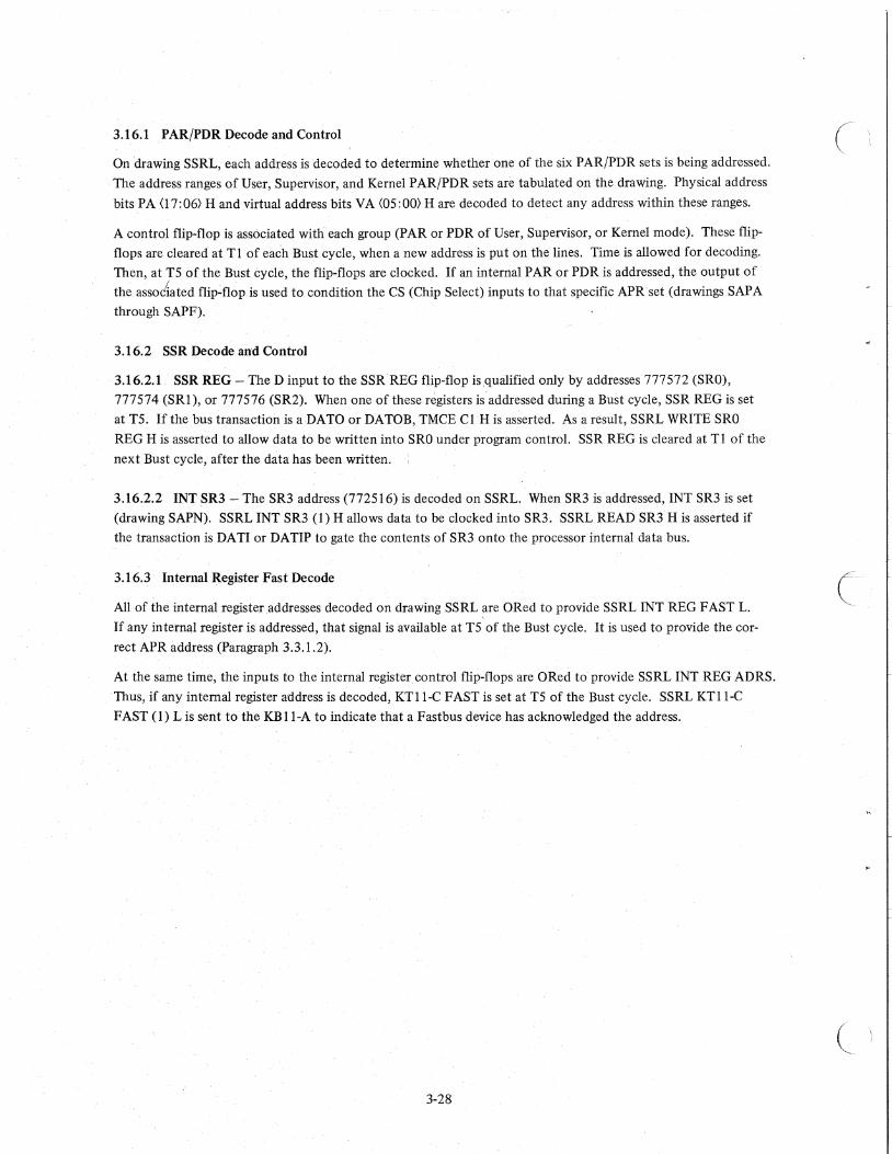
3.16.1 PAR/PDR Decode and Control
On drawing SSRL, each address is decoded to determine whether one of the six PAR/PDR sets is being addressed.
The address ranges of User, Supervisor, and Kernel PAR/PDR sets are tabulated on the drawing. Physical address
bits P A (17: 06) H and virtual address bits VA (OS: 00) H are decoded to detect any address within these ranges.
A control flip-flop is associated with each group (PAR or PDR of User, Supervisor, or Kernel mode). These flip
flops are cleared at TI of each Bust cycle, when a new address is put on the lines. Time is allowed for decoding.
Then, at T5 of the Bust cycle, the flip-flops are clocked. If an internal PAR or PDR is addressed, the output of
the assoclated flip~flop is used to condition the CS (Chip Select) inputs to that specific APR set (drawings SAP A
through SAPF).
3.16.2 SSR Decode and Control
3.16.2.1. SSR REG - The D input to the SSRREG flip-flop is qualified only by addresses 777572 (SRO),
777574 (SRl), or 777576 (SR2). When one of theser~gisters is addressed during a Bust cycle, SSR REG is set
atT5. If the bus transaction is aDATO or DATOB, TMCE Cl H is asserted. As a result, SSRL WRITE SRO
REG H is asserted to allow data to be written into SRO under program control. SSR REG is cleared at Tl of the
next Bust cycle, after the data has been written.
3.16.2.2 INT SR3 - The SR3 address (7725 16) is decoded on SSRL. When SR3 is addressed, INT SR3 is set
(drawing SAPN). SSRL INT SR3 (1) H allows data to be clocked into SR3. SSRL READ SR3 H is asserted if
the transaction is DATI or DATIP to gate the contents of SR3 onto the processor internal data bus.
3.16.3 Internal Register Fast Decode
All of the internal register .addresses decoded on drawing SSRL are ORed to provide SSRL INT REG FAST L.
If any internal register is addressed, that signal is available at T5 of the Bust cycle. It is used to provide the cor
rect APR address (Paragraph 3.3.1.2).
At the same time, the inputs to the internal register control flip-flops are ORed to provide SSRL INT REG ADRS.
Thus, if any internal register address is decoded, KTlI-C FAST is set at T5 of the Bust cycle. SSRL KTlI-C
FAST (1) L is sent to the KBII-A to indicate that a Fastbus device has acknowledged the address.
3-28
(

(-
· >---~',--.-------~-- .. --.-----.'---.. -
CHAPTER 4 INSTALLATION AND MAINTENANCE
4.1 INSTALLATION
The installation procedure for the KTll ... C Memory Management Unit option is included as part of the complete
PDP-l 1/45 system installation procedure described in the PDP-ll /45 System Maintenance Manual. When the
KTll-C is included as part of the initial PDP-II /45 system, the M8l 08 SSR module and the M8107 SAP module
are installed prior to shipment. If the KTll-C option is added to an existing PDP-l 1/45 system, the installation
procedure is straightforward. The M8ll6 SJB module is removed from slot 14 of the CPU backplane assembly
and replaced with the M8l 07 SAP module. The M8l 08 SSR module is installed in slot 13 of the CPU backplane
assembly. The KTll-C option is then ready to be checked out, using the diagnostic programs supplied with the option.
4.2 MAINTENANCE
The design, construction, and implementation of the M8l 07 SAP and M81 08 SSR modules that constitute the
KTll-C Memory Management Unit option is similar to those used in the KBll-A Central Processor and other
options. Maintenance procedures for the entire system are described in the PDP-ll /45 System Maintenance
Manual, Chapter 4. Special maintenance procedures for the KTlI-C option are included in the PDP-ll /45 Maintenance Manual, Chapter 4.
4.2.1 Diagnostic Programs
Chapter 4 of the PDP-ll/45 System Maintenance Manual includes a list of the KTlI-C diagnostic programs.
These programs are part of a complete package of basic processor and option diagnostics. The sequence of run
ningthe diagnostics is set up to completely test the KBII-A Central Processor Unit before attempting to run
KTII-C diagnostic programs, thus eliminating the KB Il-A as a possible cause of a memory management failure.
The MAIN DEC (maintenance descriptions) for each diagnostic program indicates how the program is to be loaded
and run. The program listing indicates the functional logic that is being tested by each routine. The diagnostic
programs are written along functional lines to test and exercise all the KTll-C logic.
4.2.2 Troubleshooting Test Procedures
The use of the W13l maintenance card and the W900 Extender Modules is described in Chapter 4 of the
PDP-ll /45 System Maintenance Manual.
4.2.3 Repair Procedures
Specific procedures to remove and replace integrated circuit chips are illustrated in Chapter 4 of the PDP-ll/45 System Maintenance Manual.
4-1

Term
Abort
c Address Space
BEND
BUST
Internal Register
Mode
c'-
Definition
'APPENDIX A
GLOSSARY
A processor interrupt that can occur at any memory reference, not just
between instructions. The KT1l-C will cause an abort if an address at
tempts to access a non-resident address, to write into a read-only page,. or
violates the length of a page. When the abort occurs, the KTll-C logs the
page number causing the abort, the virtual address of the instruction caus
ing the abort, and any other information necessary to process the abort;
A KTll-C abort takes a new PC from Kernel D virtual address 250 and a
new PS from252. The old PS and PC are pushed on the stack specified
by the new PS bits <14: 15).
The set of addresses used during processing in a specific processor mode
(Kernel, Supervisor, User). The Virtual Address Space is that set of ad
dresses authorized by the KTll-C for a particular mode. The Physical Ad
dress Space for the mode is the virtual address space as mapped into physi
cal addresses. In general, the Kernel, Supervisor, and User modes will op
erate out of the same virtual address space but out of different physical
address spaces.
Acronym for Bus END - meaning that the bus cycle (read "memor~"
cycle) in process is terminated. A BEND condition occurs when an antic
ipatory fetch turns out to be wrong or when some error condition is de
tected on the reference. When the BEND condition is detected in the
KTll-C logic, no abort or memory management trap can occur on the ref
erence.
Acronym for BUs STart (read "memory cycle" start). The name of the
processor state that constitutes the first half of a memory cycle. The sec
ond half of the memory cycle is designated PAUSE.
All Page Address Registers, Page Descriptor Registers, Status Registers 0,
1,2, and 3 are considered to be "internal registers".
The PDP-llj45 has three modes of operation: Kernel, Supervisor, and
User. The KTll-C provides a separate set of PARjPDR registers for use
in each of these modes. The mode is specified by bits <15: 14) in the pro
cessor status (PS) word: 00:;: Kernel, 01 = Supervisor; 11 :;: User.
A-I

Term
Operating System
PA
Page
PAR - Page Address :Register
Pause
PDR - Page Descriptor Register
Physical Address
ROM·~ Read.OiUy Memory
VA
Virtual Address
Definition
A collection of programs that provides facilities and service to a user by
allocating resources (CPU, memory, I/O) among several users .. An operat
ing system is identical to a "control" program, a "monitor" program, or
"supervisor" program. The PDP-l 1/45 is designed Ito run the operating
system in the Kernel and Supervisor modes.
An abbreviation for "Physical Address".
A collection of continuous memory addresses. The KTlI-C divides the
32K word processor address space into eight 4K sections called pages. The
lowest address in each page is a whole multiple of 4096. The length of the
page IS some whole multiple of 32 through 128. Thus, a page may vary in
size from 32 to 4096 words, in 32 word increments, and begins on a 4096
word boundary.
A register containing the "base address" or "relocation constant" associ
ated with a page. The KTlI-C has 48 PARs, 16 associated with each of
the three processor modes (User, Supervisor, and Kernel).
The term used to describe the second half of a memory cycle. During the
Pause cycle, KTllcC status registers are updated and the processor, if nec
essary, pauses to wait for completion of the current memory cycle.
A register containing information associated with a page. This includes
the length of the page, the expansion direction, and the access key. The
KTII-C has 48 PDRs, 16 associated with each of the three processor
modes (User, Supervisor, and Kernel).
The address generated by the KTlI-C that is used to select a specific mem
ory location. When the KTlI-C is operating, the "physical address" is
identical to the "relocated address".
Ahardware device that is able to store bit patterns that can be read by
providing a specific address. In the KTlI-C, four ROMs are used to con
trol modifiCations to status registers, detect exceptions, and separate
I space references from D space references.
An abbreviation for "Virtual Address".
The address generated by the PDP~II/45 processor. The term "virtual" is
applied because the address will be relocated by the contents of the PAR.
The memory location reached will be the relocated address. Hence, the
processor "thinks" i,t is addressing one location but actually gets another.
The first address is then really a dummy or ''virtual'' address.
A-2
c
(

c-
c
APPENDIX B
REFERENCE LITERATURE
The following list of references covers some of the more general aspects of memory management tasks of interest
to systems programmers. It is part of the recommended bibliography of the National Academy of Engineering for its course outline on "Operating System Principles".
The following abbreviations are used in the bibliography.
ACM IEEE IEEETC CACM JACM CS FJCC SJCC 2S0SP
Association for Computing Machinery . Institute for Electrical and Electronics Engineers IEEE Transactions on ComputerS Communications of the ACM Journal of the ACM Computing Surveys (ACM) Fall Joint Computer Conference Spring Joint Computer Conference Second .Symposium on Operating Systems Principles (proceedings available from ACM,
1133 Avenue of Americas, New York, N.Y. 10036)
Abate, J., and Dubner, H. Optimizing the Performance of a Drum-Like Storage. IEEE Trans. C-18, 11 (Nov. 1969),992-997).
Belady, L.A. A Study of Replacement Algorithms for Virtual Storage Computers. IBM Sys. J. 5, 2 (1966), 78-101.
Bensoussan, A., Clingen, C.T., and Daley, R.C. The Multics Virtual Memory. Proc. 2S0SP (Oct. 1969).
Denning, P.J. The Working Set Model for Program Behavior. Comm. ACM 11,5 (May 1968),323-333.
Denning, P.J. Thrashing; Its Causes and Prevention. AFIPS Conf. Proc. 33 (1968 FJCC), 915-922.
Denning, P.J. Virtual Memory. CS 2, 3 (Sept. 1970), 153-189.
Dennis, J.B. Segmentation and the Design of Multiprogrammed Computer Systems. JACM 12, 4 (Oct. 1965), 589-602.
Kilburn, T. et al. One-Level Storage System. IRE Trans. EC-II, 2 (Apr. 1962),223-235.
Knuth, D.E. The Art of Computer Programming (Vol. 1). Addison-Wesley (1968), Ch. 2.
Mattson, R.L., Gecsei, J., Slutz, D.R., and Traiger, I.L. Evaluation Techniques for Storage Hierarchies. IBM Sys. J. 9, 2 (1970),78-117.
Randell, B., and Keuhner, C.J. Dynamic Storage Allocation Systems. Comm. ACM 11,5 (May 1968), 197-305.
Sayre, D. Is Automatic Folding of Programs Efficient Enough to Displace Manual? CACM 12, 12 (Dec. 1969), 656-660.
Wilkes, M.V. Slave Memories and Dynamic Storage Allocation. IEEE Trans. EC-14 (Apr. 1965),270-271.
Wilkes, M.V. Time-Sharing Computer Systems. Am. Elsevier (1968).

c
A
A (Attention) Bit
for gathering statistics, 2.4.5
logic, 3.3.2.4
purpose, 2.1.3
Abort
control sequence, F3-4
decode logic, 3.6.1
flags, fonnat, 2.3.1
flags, logic, 3.11.1
mechanism, 2.1.4
processing, 2.4.B.l
recovery, F2-15
Access Control Field
ACF,2.1.2.1
detailed functions, 2.2.2.1
keys, T2-2
ACF Keys
definitions, T2-2
statistics gathering aids, 2.1.3, 2.4.5
Address
assignments, 2.2
display, 3.5.1, F3-3
drivers, 3.B
PAR/PDR assignments, T2-1
path,3.2.1
physical, F2-3
relocation, 2.1.1
relocation sequence, F3-B
selection switch, 2.4
virtual, 1.3.2
Active Page Registers, F2-5
Attention
A bit, 2.2.2.4
ATTN flip~flop, 3.3.2.4
Autodecrement/Autoincrement, 3.10.2.4,3.12.2
INDEX
B
Base Address, 2.1.1
Block Number, 2.2.2.5
Bus Pause Timing, F3"B
C
Communication Between Programs, 2.4.4
Console
operation with KTlI-C, 2.4.1.1
mode control, 3.5.2
D
Destination Mode
control logic, 3.11.4
purpose of bit, 2.3.1. 7
Dynamic Memory Allocation, 2.2.2.5
D Space
control logic, 3.10.6
PDR, 2.1.2.2
use of, 2.4.6
enable D space, 2.3.4
E
Execute-Only Protection, 1.3.1,2.1.2.2
Expansion Direction, 2.2.2.2
downward, F2-9
upward, F2-B memory, 1.3.3'
F
Fast Decode, Internal Regilters, 3.16.3
Fastbus, 3.1
I-I
Fault Detection Logic, 3.5
Fault Recovery, F2-l5
General Registers
address logic, 3.12.1
status, 2.3.2
·I/D space
G
bit of SRO, 2.3.1.9
control by SR3, 2.3.4
control logic, 3.10.6
KTll-C capability, 1.3.5
limitations, 2.4.6
Instruction Complete, 2.3 .18
bit use, 2.4.10
Interface, hardware, F3-1
Internal Registers
access timing, F3-9
control logic, 3.16
fast decode, 3.16.3
inhibit, 3.6.2
SRO, SRI, SR2, and SR3, 2.3
Inte~nal Data Bus, 3.14
K
Kernel Space address assignments, T2-J
ccintrollogic, 3.10.3
general, 1.3.7
SRO mode field, 3.11.6
INDEX (Cont)
M
Memory Expansion, 1.3.3 . \
Memory Protection, 2.1.2, 2.4.3
Memory Management
enable, 2.3.1.6
ROM,3.10
statistics, 2.1.3
status registers, 2.3
trap logic, 3.11.2
N
Non-Reentrant Programs, 2.1.2.2
Non-Resident
page fault, 3.6.1
protection, 2.1.2.1
PAR/PDR; 2-5
addresses, T2-l
description, 3.3
multiplexers, 3.7
selection, 3.3.3.1
P
Page Address Field (PAF), 2.1.1
format, F2-6
logic, 3.3.1
. Page Address Register (PAR), 2.1.1
address assignments, T2-l
contents, 2.2 format, F2-6
logic, 3.3.1
Page Descriptor Register (PDR)
address assignments, T2-l
contents, 2.2
format, F2-7
logic, 3.3.2
1-2
c

I'.
c
(
Page
expansion, 2.2.2.2
fault recovery, F2-1 5
length, 1.3.1, Tl-l
variable length, 1.3.4
Page Number, 3.11.8
Physical Address
construction, F2-3
determination, 2.4.2
display, T2-3
overlapping, 2.4.4.1
no. virtual address, 1.3.2
Power Requirements, Tl-l
Processor Status Word, 2.1.2.3
modification, 2.4.8
Protection
kernel mode, 2.4.7.1
memory, 1.3.1
PS Restore, 3.10.2.1
PSW Bits, Current Mode, 2.1.2.4
Read-Only
fault logic, 3.6.1.2
protection, 2.1. 2.1
R
Read-OnlyMemory (ROM), 3.10.1
Recovery
from abort, 2.4.10
from I/O lockout, 2.4.7.2
routine, flow chart, F2-15
Reentrant Programs, 2.1.2.2
Relocation
address relocation, 2.1.1
block diagrams, F2-1, F2-2
definition, 1.3.2
logic, 3.4
timing, F3-8
INDEX (Cont)
ROM
organization, 3.10.1
output decode, T3-3
SAP Module M81 07
functions, F3-2
installation, 4.1
location, Tl-l
SSR Module M8l 08
functions, F3-2
installation, 4.1
location, Tl-l
Stack
S
communication, 2.4.4.2
downward expandable page, 2.2.2.5
no program, 1.3.8
Statistics
gathering routine, 2.4.5
memory management, 2.1.3
Status Registers
format
logic
SRO, 2.3.1
SRl,2.3.2
SR2,2.3.3
SR3,2.3.4
SRO, 3.11
SRl,3.12
SR2,3.13
SR3,3.9
Supervisor Space
address assignments, T2-1
control logic, 3.10.4
general, 1.3.7
SRO mode field, 3.11.6
Swapping, 2.1.3
1-3
T-Bit, 2.3.3 SR2logic, 3.13
Timing
Trap
diagram, F3-7 event times, T3-5
T
control logic, 3.11.2
control sequence, F3-5
decode logic, 3.6.3
flag format, 2.3.1.4
memory management, 2.3.1.4
vector addresses, 2.4.11
Trap/Abort
mechanism, 2.14
recovery, F2-l5
Unibus
address drivers, 3-8
interface, F3-1
NOTE: T = Tables and F '" Figures.
U
INDEX (Cont)
User Space address assignments, T2cl
controllogic,3.10.5
general, 1.3.7
SRO mode field, 3.11.7
v
Virtual Address
display, T2-3
inverters, 3.4.1
page numbers, 2.2
program counter, 2.3.3
vs physical addresses, 1.3.2
W (Written Into) Bit
logic, 3.3.2.4
purpose, 2.1.3
written into, 2.2.2;2
IA
w
(

(
(
(
READER'S COMMENTS
KT11-C MEMORY MANAGEMENT UNIT MAINTENANCE MANUAL DEC-II-HKTB-D
Your comments and suggestions will help us in our continuqus effort to improve the quality and usefulness of
our pUblications.
What is your general reaction to this manual? In your judgment is it complete, accurate, well organized, well
written, etc.? Is it easy to use?
What features are most useful? ------------------------------------------------
What faults do you find with the manual? ------------------------------
Does this manual satisfy the need you think it was intended to satisfy? _______________ _
Does it satisfy your needs? Why?
Would you please indicate any factual errors you have found.
Please describe your position.
Name ___________________ ___ Organization ________ ,.-------_--
Street ________________ _ Department
City ___________ _ State Zip or Country _________ _

- - - - - - - - - - - - - - - - Fold Here - - - - - - - - - - - - - - - ,..... - - - - -
- - - - - - - - ..;.. - - - - Do Not Tear - Fold Here and Staple - - - - - - - - - - - - -
BUSINESS REPLY MAIL
NO POSTAGE STAMP NECESSARY IF MAILED IN THE UNITED STATE'S
Postage will be paid by:
Digital Equipment Corporation Technical Documentation Department 146 Main Street Maynard, MassachuSetts 01754
FIRST CLASS PERMIT NO. 33
MAYNARD, MASS.
i( ! I


DIGITAL EQUIPMENT CORPORATION MAYNARD, MASSACHUSETTS 01754