KiwiSDR design review - GPS cape for the BeagleBone...
65
KiwiSDR design review Version 2.1 – February 2016 John Seamons, ZL/KF6VO [email protected] Summary This document describes the design of KiwiSDR , a software-defined radio (SDR) add-on board (so-called "cape") for the popular BeagleBone Black single-board computer. Although the first PCBs have been constructed, design feedback is still sought from experts in the community before more units are manufactured. Click for the live receiver in New Zealand . There are also now two beta units, at the University of Victoria, B.C., Canada and the SK3W Contest Station, Sweden . The KiwiSDRs are registered on the SDR.hu network . Complete sources are on github . The design is open-source / open-hardware with full details available to anyone (including PCB layout). The project leverages much existing open SDR technology, but especially the pioneering work of Pieter-Tjerk de Boer, PA3FWM, the creator of WebSDR , Andrew Holme's Homemade GPS Receiver and OpenWebRX from András Retzler, HA7ILM. If a reasonable retail price target can be achieved the intent is to produce and sell boards. Some form of crowd funding is being considered to bootstrap initial production and fund up-front costs such as regulatory compliance testing. The minimum-threshold aspect of crowd funding will also provide a good estimate of overall interest in the project given how crowded the SDR space is these days. TOC 1 © bluebison.net
Transcript of KiwiSDR design review - GPS cape for the BeagleBone...

KiwiSDR design reviewVersion 2.1 – February 2016
John Seamons, ZL/[email protected]
Summary
This document describes the design of KiwiSDR, a software-defined radio (SDR)add-on board (so-called "cape") for the popular BeagleBone Black single-boardcomputer. Although the first PCBs have been constructed, design feedback is still sought from experts in the community before more units are manufactured. Click for the live receiver in New Zealand. There are also now two beta units, at the University of Victoria, B.C., Canada and the SK3W Contest Station, Sweden. The KiwiSDRs are registered on the SDR.hu network. Complete sources are on github.
The design is open-source / open-hardware with full details available to anyone (including PCB layout). The project leverages much existing open SDR technology, but especially the pioneering work of Pieter-Tjerk de Boer, PA3FWM, the creator of WebSDR, Andrew Holme's Homemade GPS Receiver and OpenWebRX from András Retzler, HA7ILM.
If a reasonable retail price target can be achieved the intent is to produce and sell boards. Some form of crowd funding is being considered to bootstrap initial production and fund up-front costs such as regulatory compliance testing. The minimum-threshold aspect of crowd funding will also provide a good estimate of overall interest in the project given how crowded the SDR space is these days.
TOC 1
© bluebison.net

How you can help
I welcome advice of any kind. Especially if you see an error or misconception on my part. There is also a list of open questions at the end of each description section you can help answer. A lot of the design is "cookbook" based on my limited understanding of certain areas (e.g. RF design, EMI/EMC). Even if you only read one paragraph, and email one comment ([email protected]), you will be doing me a huge favor. Sincere thanks in advance. (click on user interface images below for full size)
TOC 2

Table of Contents (clickable) 1 Objectives 6 2 Description and Features 6 3 Applications 7 4 Status 7 5 Design Philosophy 7
5.1.1 Price-point and trade-offs 7 5.1.2 Active antenna 8 5.1.3 Beagle as host 8 5.1.4 Enclosure 8 5.1.5 Mission creep 8 5.1.6 Second generation 8
6 Detailed Design Description 9 6.1 Hardware overview 9 6.2 Software Overview 13 6.3 VLF-HF SDR 14
6.3.1 Front-end 14 6.3.2 ADC 14 6.3.3 ADC clock 14 6.3.4 Performance 15 6.3.5 FPGA logic 15 6.3.6 IQ mixer 16 6.3.7 CIC Filters 17 6.3.8 Audio channels 17 6.3.9 CIC filter optimization 17 6.3.10 No FIR filter hack – audio 18 6.3.11 Waterfall channels 18 6.3.12 Waterfall overlapped sampling 19 6.3.13 No FIR filter hack – waterfall 19 6.3.14 Baseband processing 20
6.4 Software-Defined GPS Receiver 21 6.4.1 Front-end 21 6.4.2 GPSDO possibilities 21 6.4.3 FPGA logic 21 6.4.4 Logic optimization 23 6.4.5 Software 23 6.4.6 ADC clock frequency correction via GPS timing 23
6.5 Beagle Cape Interface 24 6.5.1 SPI 24 6.5.2 Expansion port 24 6.5.3 EEPROM 24
6.6 Power supplies 25 6.6.1 Custom Beagle power supply 25 6.6.2 Interaction with Beagle 25 6.6.3 5V input internal / external source select 25
TOC 3
6.6.4 3.3V digital from Beagle 25 6.6.5 FPGA power-up sequencing 26 6.6.6 1.0V SMPS 26 6.6.7 3.3V analog rail LDOs 26 6.6.8 Current requirements & power dissipation analysis 26
6.7 Active Antenna 30 6.7.1 Version schematics 30 6.7.2 Coupling bandwidth 30 6.7.3 Transistor selection 30 6.7.4 Power supply 31 6.7.5 Bias tee 31 6.7.6 Feed-line connection 31 6.7.7 Grounding 32 6.7.8 Enclosure 32
6.8 Active Antenna – Power Injector (bias tee) 33 6.8.1 Filtering 33 6.8.2 Input protection 33 6.8.3 Voltage & current distribution 33 6.8.4 Diode noise 34 6.8.5 Bias tee 34
6.9 Software 35 6.9.1 Source code 35 6.9.2 Embedded CPU (eCPU) 35 6.9.3 Beagle application 35 6.9.4 FPGA development 37 6.9.5 Verilog 38 6.9.6 Version checking, serial number 38
7 PCB 39 7.1 BeagleBone cape compatibility 39
7.1.1 PCB size 39 7.1.2 Beagle interface 40
7.2 Mixed-signal PCB design 40 7.2.1 General layout 40 7.2.2 RF shields 42 7.2.3 GPS 42 7.2.4 ADC 42 7.2.5 Edge via stitching 42
7.3 PCB specifications 43 7.3.1 Layer count 43 7.3.2 Surface finish 43 7.3.3 PCB stackup 43 7.3.4 Layer assignment 44 7.3.5 Controlled impedance 44
7.4 Layout design rules 44 7.4.1 Unit choice and layout grid 44 7.4.2 Traces and vias 44 7.4.3 SMD pad connection to planes 45
TOC 4

7.4.4 Planes / zones 45 7.5 Other PCB elements 46
7.5.1 Fiducials 46 7.5.2 Tooling holes 46 7.5.3 Panelization 46 7.5.4 Edge keepout 46 7.5.5 Test pads 46 7.5.6 Layer ID 46
7.6 Thermal / RF ground via-in-pad 46 7.6.1 Existing solutions 47 7.6.2 KiCAD footprint solution 47
7.7 FPGA BGA issues 50 7.7.1 Power planes 50 7.7.2 Traces and vias 54 7.7.3 Bypass caps 55
8 EMC / EMI 57 8.1.1 Proximity to Beagle 57 8.1.2 SMPS switching transient propagation 57 8.1.3 Clock harmonics within the GPS L1 bandwidth 57 8.1.4 Certification 59
9 DFM 61 9.1 Parts commonality 61 9.2 Minimizing high assembly-cost parts 61
9.2.1 Through hole 61 9.2.2 Fine pitch 61
9.3 Placement spacing 61 9.4 BGA inspection clearance 61 9.5 QFN pad pullback 62 9.6 Copper warping / twisting during reflow 62 9.7 SMD tombstoning / shifting 62 9.8 Reverse header soldering 62 9.9 Test methodology 63
9.9.1 RF source 63 9.9.2 JTAG 63
10 Bill of Materials 64 11 Schematics and Files 65 12 Risks 66 13 Abbreviations 67
TOC 5
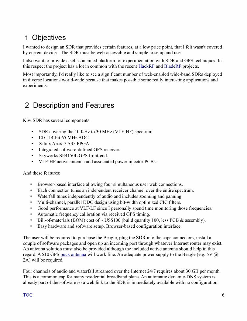
1 ObjectivesI wanted to design an SDR that provides certain features, at a low price point, that I felt wasn't covered by current devices. The SDR must be web-accessible and simple to setup and use.
I also want to provide a self-contained platform for experimentation with SDR and GPS techniques. In this respect the project has a lot in common with the recent HackRF and BladeRF projects.
Most importantly, I'd really like to see a significant number of web-enabled wide-band SDRs deployed in diverse locations world-wide because that makes possible some really interesting applications and experiments.
2 Description and Features
KiwiSDR has several components:
• SDR covering the 10 KHz to 30 MHz (VLF-HF) spectrum.• LTC 14-bit 65 MHz ADC.• Xilinx Artix-7 A35 FPGA.• Integrated software-defined GPS receiver.• Skyworks SE4150L GPS front-end.• VLF-HF active antenna and associated power injector PCBs.
And these features:
• Browser-based interface allowing four simultaneous user web connections.• Each connection tunes an independent receiver channel over the entire spectrum.• Waterfall tunes independently of audio and includes zooming and panning.• Multi-channel, parallel DDC design using bit-width optimized CIC filters.• Good performance at VLF/LF since I personally spend time monitoring those frequencies.• Automatic frequency calibration via received GPS timing.• Bill-of-materials (BOM) cost of ~ US$100 (build quantity 100, less PCB & assembly).• Easy hardware and software setup. Browser-based configuration interface.
The user will be required to purchase the Beagle, plug the SDR into the cape connectors, install a couple of software packages and open up an incoming port through whatever Internet router may exist. An antenna solution must also be provided although the included active antenna should help in this regard. A $10 GPS puck antenna will work fine. An adequate power supply to the Beagle (e.g. 5V @ 2A) will be required.
Four channels of audio and waterfall streamed over the Internet 24/7 requires about 30 GB per month. This is a common cap for many residential broadband plans. An automatic dynamic-DNS system is already part of the software so a web link to the SDR is immediately available with no configuration.
TOC 6
Of course the system can be configured to only allow connections from the local network and ignore Internet connection requests.
3 ApplicationsIn addition to simply monitoring signals a number of applications and experiments are possible.
Applications possible if many KiwiSDRs are deployed world-wide:
• Time-of-arrival direction finding, assisted by having accurate GPS time & location info.(similar to the VLF TOA/TOGA lightning detection of blitzortung.org)
• Experiments with location-diversity reception, as opposed to the usual frequency-diversity.• Source of world-wide data for GPS common-view experiments.
Other applications:
• Education and experimentation platform for SDR and SD-GPS techniques.• Decoder for WWVB's new PSK modulation format (similarly with DCF77 in Germany)• Weak signal integration detection.• Development of speciality I/Q demodulators. A WSPR decoder has been demonstrated.
4 StatusThe schematic and layout have been captured using KiCAD. Several PCBs have been fabricated and assembled. BOM output from KiCAD is post-processed to provide a file suitable for uploading to octopart.com for quotation.
FPGA Verilog and application code development is working and draws on the efforts of many open-source projects. System bandwidth / throughput analysis has been made. The contract manufacturer who built the prototypes has quoted me a very attractive price for building 100 units.
5 Design PhilosophyKiwiSDR attempts to fit in the cost and performance gap between USB dongle-style, or fixed DDC chip, devices ($20 - $200, 8-12 bit ADC) and full 16-bit SDRs ($700 - $3500). At the same time offering wide-band, web-enabled capabilities not always found even on the more expensive SDRs.
5.1.1 Price-point and trade-offs
Given the BOM cost, a possible retail price is very roughly in the US$250 - $350 range. There have been no calculations for distribution or other indirect costs yet. Since many of the applications require a significant number of units being placed world-wide a low price-point is essential. Ruthless trade-offs in component choice vs specifications are required (e.g. $24 14-bit @ 65 MSPS ADC vs $80 16-bit @
TOC 7
130 MSPS).
5.1.2 Active antenna
The idea is to include the PCBs for an active antenna and associated power injector as part of the project. This way a user could get the receiver working by only having to add an antenna enclosure, feed-line and AC power source. The (components) BOM incremental cost to do this is only about 10%, similar to the cost of adding the SD-GPS. For manufacturing these additional PCBs would simply be part of a larger panelized design with appropriate slot routing and break-away tabs.
Inclusion of the active antenna is very much an open question however. Perhaps it is best sold as an added cost option.
5.1.3 Beagle as host
Using the US$55 BeagleBone Black as the host is an absolute no-brainer from every perspective. For the money that kind of equivalent functionality cannot be designed into the SDR. Since the intent is for the user to leave the SDR connected to the Internet full-time a solution requiring a dedicated PC is much less attractive. As of early 2016 there is a compatible, but even lower cost, BeagleBone Green for US$39. It lacks the HDMI interface, which we don't use anyway, and is simply a potential source of interference.
5.1.4 Enclosure
The intent is to sell the board without an enclosure. There are existing enclosures for the Beagle although most do not meet the size requirements given our extended-length PCB. It is possible a top/bottom acrylic plate design similar to early HackRF units could be made.
5.1.5 Mission creep
I specifically avoided adding any SRAM external to the FGPA or bringing additional FPGA I/Os out to an expansion connector for cost and possible noise-source reasons (and also the time and complexity to route those PCB traces and validate the functionality of the interfaces). A second generation of the board might include them. But note that expansion I/Os to the Beagle are included.
5.1.6 Second generation
A second generation of the board might also include a Gigabit Ethernet PHY and RJ45 since open-source GE MAC FPGA cores are pretty common. This would allow experimentation with full bandwidth FFT-based SDR techniques as opposed to DDC (the openHPSDR folks are calling this technique "Direct Fourier Conversion" [DFC] – essentially what WebSDR uses). There has also been the idea of including UHF/VHF spectrum capabilities such as a low-cost AIS (marine vessel tracking at 162 MHz) and ADS-B (aircraft tracking at 1090 MHz). Maybe this is best done with a daughter board.
TOC 8

6 Detailed Design Description
The design can be divided into seven parts:
• VLF-HF SDR• Software-Defined GPS receiver• Beagle cape interface• Power supplies• Active antenna• Active antenna power injector (bias tee)• Software
6.1 Hardware overviewThe hardware overview diagram below shows the major components of the board.
Inside the RF shield cans are the SDR and GPS front-end circuits. The SDR has a 30 MHz LPF and +20 dB preamp ahead of the ADC. A 65 MHz XO clocks the ADC and is one of the clock inputs to the FPGA.
The GPS front-end chip has a 16.384 MHz TCXO which similarly clocks the FPGA.
Communication with the Beagle is over the standard cape 0.1” header connectors. All data is moved over a 48 MHz SPI link. The FPGA is downloaded from the application running on the Beagle. Additional Beagle I/Os are connected to the FPGA for future expansion, e.g. a higher performance parallel port. An EEPROM containing cape header-use configuration information is provided according to the Beagle specification.
TOC 9

Most of the board power is provided from regulators connected to the 5V source from the Beagle that passes through the headers. Only some 3.3V is taken from the Beagle directly to run the FPGA IO pins and the EEPROM. A switching regulator provides the relatively high current for the FPGA core while linear LDOs are used for the remaining supplies including quiet supplies for the ADC and GPS.
The FPGA Clock Domains diagram below shows the Verilog module organization inside the FPGA. The built-in dual-port 36 kbit BRAM (block RAM) memories of the FPGA provide isolation between clock domains, as well as some synchronization primitives I wrote. The bus looking structure in the middle is really a series of dedicated connections, many of which are multiplexed. The SPI and eCPU blocks are from Andrew Holme's open-source Homemade GPS Receiver.
The eCPU is a tiny 32-bit stack-based embedded CPU Andrew designed. The eCPU instruction memory is downloaded over the SPI after the FPGA is programmed. In addition to Andrew's code to support the GPS I added code to efficiently control registers in the SDR logic and assist with data transfer to the SPI. The eCPU runs at the modest 16 MHz clock to make synchronization with the GPS logic easier.
TOC 10

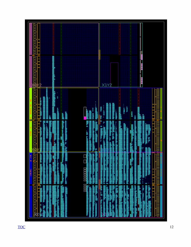
The image below is the floor-plan of the FPGA. The Xilinx A35 can currently fit 4 SDR channels along with a 12 channel SD-GPS and one eCPU.
The device utilization is:
• 60% of the logic slices• 93% of the BRAMs• 40% of the DSPs
The limiting factor is the number of BRAMs in this configuration. So a design with a more efficient use of BRAMs might allow another SDR channel to be added. Up to 16 GPS channels (and likely more) will fit because each additional tracking demodulator only requires an additional two DSP slices and no additional BRAMs. But in practice more GPS channels don't seem to be needed.
Note that since the audio and waterfall DDCs are independently tunable (and zoomable in the case of the waterfall) this means there are really 8 distinct DDCs in the FPGA.
TOC 11
TOC 12

6.2 Software OverviewThe figure below shows the distribution of the software signal processing tasks (including Verilog). The FPGA only performs DDC at the audio channel bandwidth and at the selected visible spectrum span. The FFT and baseband audio processing are performed on the Beagle. Finally, the user's browser, via Javascript, converts the FFT output into the waterfall and spectrum displays. The audio stream is interpolated from the 8.25 kHz Internet transport rate to the native audio output rate (typically 44.1 or 48 kbps but others are supported). These tasks are repeated for each simultaneous receiver channel and corresponding internet browser connection.
TOC 13

6.3 VLF-HF SDR
6.3.1 Front-end
Referring to the ADC schematic, the antenna connection is via a 2 position screw-post terminal block. As detailed in the active antenna section the use of a terminal block for the connection of bare wires is in the interest of simplicity. In parallel to that PCB pads exist for an edge-launch SMA or BNC connector.
A low-capacitance TVS across the input attempts to provide some transient protection.
Next are two parallel DC blocking caps. A range of values are used to be somewhat broadband. This is followed by a 7-pole Chebyshev 30 MHz low pass filter from EI9GQ. Transformer 1:4 coupling (50 to 200Z) to the preamp was considered, but I wasn't able to find one that fit the height requirement of the RF shield and still had a low enough frequency response (which is proportional to transformer size). The Mini-Circuits TC4-1TX is “useable” to 200 kHz according to the data sheet. It would fit but probably has unacceptable attenuation at 10 kHz. So single-ended resistive impedance matching was done using the values specified in table 5-4 of LTC app note 123. A 40 MHz LC LPF follows to band limit the preamp broadband noise. The LTC 6401-20 +20 dB differential ADC driver preamp is several generations old but very reasonably priced. The high performance of the latest generation devices is not required at these low frequencies.
Some SDRs include a software-selectable attenuator before the preamp. This was left out for cost reasons. Experience has shown that a 14-bit ADC has sufficient dynamic range using an active antenna with “shortwave receiver”-level performance goals.
6.3.2 ADC
The LTC2248 14-bit 65 MHz ADC is relatively inexpensive ($28 Q100) compared to 16-bit and > 65 MHz clock rate parts. I am willing to accept a performance compromise above 25 MHz (close to Nyquist) in exchange for a cheaper ADC as this SDR is not intended to be a receiver with exceptional performance on the 10 meter Ham band. It would be nice to use a part with LVDS outputs for EMI reasons but they are twice as expensive.
Series resistors on the ADC end of all digital outputs will be used to limit edge rates and switching noise. The value of 100R comes from page 3 of this app note assuming a 65 MHz sample clock and worst case 15 pF output loading.
6.3.3 ADC clock
The clock is a Conner-Winfield CWX823 series XO which is a reasonably priced oscillator ($2) with good phase noise performance (< 1ps rms phase jitter). But as several excellent LTC app notes mention (here and here) one has to be very careful about drawing conclusions from published phase noise specs. Fortunately, clock jitter is going to translate into much less ADC noise with a 65 MHz sample clock
TOC 14
than by using, say, an ADC with a 400 MHz clock. The clock jitter vs SNR vs frequency graphs in the app notes make this clear.
The XO output drives the ADC with as short a connection as possible, but also drives a NC7Z126 buffer connected to the FPGA as suggested by the ADC data-sheet. Any frequency error is corrected in the software with GPS timing as described in the SD-GPS section.
Questions:• Anyone have a favorite low-cost ADC clock part suggestion?
6.3.4 Performance
No dynamic range or noise-figure analysis has been made yet. PA3FWM told me that his WebSDR never seems to toggle the top two bits of his 16-bit ADC even with the strong LW & BCB signals at the receiver location. Noise floor and spurious response will just have to be empirically measured. Same for other performance metrics such as strong signal handling and effectiveness of the 30 MHz LPF.
6.3.5 FPGA logic
The figure below shows the classic digital down-conversion (DDC) architecture of the SDR. The audio and waterfall Verilog code is replicated for as many channels as are configured.
TOC 15

6.3.6 IQ mixer
Each DDC begins with an IQ mixer. Traditionally the DDS part is implemented with a CORDIC configured to generate the sin/cos clocks for the mixers and in most cases to simultaneously do the mixer multiplies as well (see openHPSDR's Hermes or James Ahlstrom's HiQSDR project Verilog for examples). But with the DSP slices modern FPGAs provide there is no need to use CORDIC anymore.
The Xilinx Vivado design tool has license-free DDS “intellectual-property (IP)” generators that are easy to use. A DDS configured with a 32-bit phase increment input, 15-bit output and internal 13-bit phase angle uses only one 36 kbit BRAM for the lookup table and 0-2 DSP slices (option) for the phase accumulator. The last two bits of effective phase angle are the result of some phase dithering applied to the output. This results in a 90 dB SFDR which is pretty good. Without the dithering, achieving 90 dB
TOC 16

would require 3.5 BRAMs which are the limiting factor in our design.
Two DSP slices are used for the mixer multipliers.
When I originally tried the Verilog CORDIC with multiple channels I immediately ran out of the limited number of logic blocks that support the carry-chains needed by the long adders (typically 1/3 – 1/2 of the total number of logic blocks depending on the FPGA). This problem is compounded by the long adders used in the CIC filters. 22-bits are used from the mixer multipliers as inputs to the CIC filters.
6.3.7 CIC Filters
Several implementations of the Cascaded Integrator-Comb (CIC) filter in Verilog were developed. These were written mostly to decrease the number of logic slices used given the large number of CICs in the SDR. They are described below.
6.3.8 Audio channels
Two cascaded CIC filters, CIC1 and CIC2 are used as is seen in most SDR designs. CIC1 is a 3 stage filter with 18 output bits and a decimation of 256. CIC2 is a 5 stage filter with 24 output bits and a decimation of 31. It was found that 24-bits was needed to get sufficient dynamic range in the audio. This is not surprising given that the AGC occurs downstream from this point. This gives an audio rate of 8.25 kHz which is a convenient number for the built-in WSPR data demodulator. It will probably be made wider eventually.
One issue I have never found an explanation for is why you typically see two separate CIC filters cascaded together. I understand the effect of increasing the number of stages in a single filter and how filter bit-growth is a function of stages and decimation factor. For example, I implemented the waterfall by splitting the decimation across two CICs and compared it to performing all the decimation in a single stage and there was no visible difference at all. Sure, the single CIC version will have vastly longer registers due to the increased decimation (87-bits for decimation 256*31=7936 and 22-bits of input). Maybe the difference has to do with power consumption and speed limitations of older FPGA devices. With a single CIC all of those 87-bit integrator registers and adders are clocking at the full ADC sample rate. Older FPGAs might not have been able to do carry-propagation for those longer adders at the required clock rate. The other possibility is that the composite filter response of two cascaded CICs of different stage lengths is more efficient than a single CIC.
Questions:• Can anyone explain the reasons for cascading multiple CICs seen in so many SDR designs? Is it
simply for the reasons I mention? (Some feedback I've received says yes)
6.3.9 CIC filter optimization
Several optimizations have been made. One that is particularly useful in saving logic slices is an implementation of an algorithm to optimally prune the length of the registers, and hence adders, used in the filters. This is possible for example with CIC2 because only the upper 24 output bits are being used
TOC 17

of the 48-bit comb register length. This introduces a certain level of quantization error. The error can be back-propagated up through the comb and integrator stages, successively shortening the register length of each stage just to the point of maintaining the error level, but not adding to it. A section on my website describes the implementation which is automatically run from the Makefile of the project and auto-generates the necessary Verilog files.
Another optimization is to note that since decimation in a CIC is usually performed between the integrator and comb sections the comb section of CIC2 is only clocked at 8.25 kHz. This is slow enough that a fully sequential implementation is possible, using only one 48-bit DSP slice to replace all the adders and 1/2 BRAM to replace the registers. A little state machine coordinates the sequential movement of data. This is currently used in the audio channels and saves many logic slices. There is also the possibility of processing all the CIC2 combs across all the audio channels in a single sequential module if there are sufficient state machine cycles to do so. This experiment remains to be done. This processing could even be done on the Beagle, but it requires roughly twice as much data per channel be moved across the SPI. An even more ambitious experiment would be to sequentialize starting at the comb section of CIC1. The CIC1 decimation factor would likely have to be increased to slow down the output rate enough to have sufficient sequential processing clock cycles.
6.3.10 No FIR filter hack – audio
Traditionally an FIR filter follows the CIC to correct the CIC passband droop (i.e. sinc-shaped response, see figure 11). For the audio channels the FIR can be easily done on the Beagle at the audio rate. But in hardware the FIR is somewhat expensive to implement, especially since there are 8 DDCs in total. However it was found that the post-CIC FIR requirement for the audio could be side-stepped in a slightly disgusting way. The decimation is set 2x lower which passes 2x more audio bandwidth to the Beagle than needed. Now only the first half of the CIC uncompensated response is used where the droop is within 2 or 3 dB which is fine for our purposes. The rest of the data is simply thrown away. There is already an adjustable FIR filter used by the demodulators that does the ultimate bandpass filtering. So an additional FIR running on the Beagle isn't required. See below for what was done with the waterfall. The FIRs on the Beagle are implemented with FFT convolution. It has been pointed out to me that CIC droop compensation can be applied to the FFT output of the FIR filter by simple multiplication. This would solve the problem nicely.
6.3.11 Waterfall channels
In many SDR programs the waterfall/spectrum display shows the entire maximum bandwidth of the receiver (“bandscope” or “panadapter” in ham radio terminology). Sample data for the display FFT comes directly from the ADC at the full sample rate, but in low-throughput chunks. A second waterfall derived from audio channel data may show just the bandwidth of the audio channel before any post-DDC passband filtering (typically < 10 kHz). In contrast, the WebSDR waterfall is a full Zoom FFT acting more like a traditional spectrum analyzer. This has the nice effect of allowing you to be listening on a set frequency while panning and zooming the waterfall anywhere else in the spectrum looking for more signals. In our case this requires that the waterfall be implemented with a separate DDC. So in effect our 4 channel SDR is really 8 fully independent DDC channels.
To provide the 12 levels of zooming the waterfall CIC filters implement power-of-two variable
TOC 18
decimation from 1 (pass-through mode) to 1024. For a 2048-point FFT, mapping to a 1024 pixel display (to give a sharp looking display), this gives an RBW of ~30 kHz at minimum zoom (span 30 MHz) and RBW ~15 Hz at maximum zoom (span ~15 kHz). The FFT used is actually 8192 points due to the FIR filtering hack mentioned below. So this requires a sampler memory of 8k samples. 16-bits was found to be the optimum bit width for full display dynamic range.
6.3.12 Waterfall overlapped sampling
An interesting issue occurs with the waterfall generation at higher zoom levels. There is a crossover point at which it takes more time to accumulate samples for the waterfall FFT than the desired screen update rate. An example: Suppose you want a waterfall that updates at 50 Hz / 20 msec (i.e. draws 50 display lines/sec). Samples for an FFT need to be time-continuous at the full sample rate. So at minimum zoom 8k samples need to be taken at 65 MHz. This takes 126 usec. No problem doing that every 20 msec.
Now consider a waterfall zoomed in 1024x (RBW ~64 Hz, span ~64 kHz). It takes 1024 times as long to accumulate the 8k samples because the DDC has to process 8k*1024 samples at 65 MHz to output 8k samples after decimation. This takes 63 msec. Obviously a problem when trying to update every 20 msec.
This is generally known as the “ acquisition time problem”. One solution is to overlap the sampling. There is no reason you have to construct each display line from non-overlapping samples taken 63 msec apart resulting in a display that only updates at 16 Hz. Every 20 msec you can simply look at the previous 20 msec worth of data in the sampling buffer while the DDC runs along taking 63 msec to capture 8k worth of new samples. This works just fine.
Interestingly, the WebSDR has a similar consideration in the frequency domain since it is FFT not DDC-based. A multi-megapoint FFT running on a GPU being fed the full ADC bandwidth over gigabit Ethernet, which is how it supports hundreds of simultaneous users (some design details are here). A truly astonishing feat in my opinion.
6.3.13 No FIR filter hack – waterfall
Implementing a CIC-compensation FIR filter for the waterfall is even more problematic than for the audio because of the variable decimation used, e.g. at zoom decimation 2 the FIR must run at 32 MHz. Like the audio case the FIR is side-stepped by decimating 2x less, passing 2x more data and computing a 2x larger FFT on the host. The upper half of the FFT output which contains amplitude values that are distorted by the attenuated CIC input data are simply throw away. This makes computational sense since an FFT is an O(N log2N) process, i.e. an 8k FFT doesn't take much longer than a 4k. For example at zoom level 3 (span 3.75 MHz) the waterfall decimation is set to 2^(3-1)=4 (span 7.5 MHz) instead of 2^3=8 and the upper half of the FFT ignored. Coincidentally it was found that trying to use the full CIC passband didn't work anyway. The upper half was usually filled with aliasing artifacts, probably a result of our low ADC clock rate to max ADC input frequency ratio. The same post-FFT gain adjustment as in the audio channels can be used to compensate for the CIC droop.
Questions:
TOC 19

• I have a bad feeling I'm missing the importance of having the FIR filter before the FFT. But the waterfalls look fine and the audio sounds pretty good. This aspect needs more research and testing. Any advice? Remember that high-performance is not a goal with this SDR.
6.3.14 Baseband processing
After the DDCs the data stored in the FIFOs and sample memories are transferred to the Beagle where all baseband processing occurs. For audio this is bandpass filtering, AGC, demodulation and S-meter generation. For the waterfall it is the FFT and display processing.
TOC 20

6.4 Software-Defined GPS Receiver
Although Andrew Holme's Homemade GPS Receiver website has an excellent detailed description a simplified explanation will be given here along with our differences. Our intent is not to implement a GPSDO but to use the GPS timing to adjust our SDR frequency to compensate for the 65 MHz ADC XO frequency error. Sort of a software frequency-locked loop (FLL).
6.4.1 Front-end
Referring to the GPS schematic, rather than Andrew's L1 front-end built from discrete components I used an inexpensive, off-the-shelf, single chip solution (Skyworks SE4150L). A 50Z controlled impedance trace is used from the SMA connector to the chip. The chip plus external components creates a bias tee for active antennas and is short-circuit protected. I have successfully prototyped using this chip.
The clock is a standard GPS-specification 0.5 PPM TCXO. Being located inside the RF shield should help minimize temperature variation. You could even imagine the shield box holding in a small block of insulating foam. The chip provides a regenerated clock output which connects to the FPGA. The current SD-GPS firmware only uses the sign data from the ADC of the chip but the magnitude data line is also connected. At greater cost ($6.50 vs $2.50), and package size, a MAX2769B could have been used so that Galileo / GLONASS / Compass could be received in addition to GPS (FPGA changes required of course). This is probably better left for a second generation board where the price target is raised a bit. The MAX2769 does suffer from annoyingly incomplete documentation.
6.4.2 GPSDO possibilities
If anyone knows of some simple hardware changes that could be made to enable actual GPSDO experimentation I'd really like to know. There is a DNL U.FL connector and coupling cap for supplying an external clock input. But any experimentation is probably limited by the quality of the L1 PLL inside the chip. But I don't understand enough about GPSDO issues to know.
Questions:
• Any opinions about this from you GPSDO experts?
6.4.3 FPGA logic
The following simplified diagram shows the GPS FPGA logic. For signal acquisition a simple memory gathers sequential 1-bit samples from the GPS front-end. The memory depth is chosen to match the width of the subsequent FFT done on the Beagle. The second port of the memory has a different aspect ratio providing 16-bit words to the SPI.
For each GPS tracking channel an identical demodulator is used. Each maintains a code and carrier NCO using classic techniques: an early-punctual-late DLL for the code and a Costas loop for the carrier. All the logic runs at the 16 MHz GPS clock except for the blocks in cyan which are implemented by code in the FPGA eCPU at a slow 1 kHz update rate. The 50 Hz GPS navigation data
TOC 21

is extracted from the carrier loop and passed onto GPS position solution code running on the Beagle.
Because most of the data paths are only one bit wide the logic functions are greatly simplified: multiplying mixers become XOR gates, full sin/cos NCOs become just phase accumulators using the msb as output, etc.
TOC 22

6.4.4 Logic optimization
Because the logic is identical you could imagine, for an 8 channel receiver, running a single demod instance at 8*16M = 128 MHz by multiplying up the GPS clock using an internal FPGA clock PLL. And then using distributed memory for intermediate storage of any channel state (integrators, NCO and C/A registers, etc.) Whether this would result in any overall logic savings or not is debatable, but it would make for an interesting experiment (there are the increased power dissipation and synchronization issues to consider).
6.4.5 Software
I have done some simple experiments with Andrew's GPS program, mostly in the process of trying to understand the code and GPS principles in general. Otherwise the code is largely unchanged.
One interesting experiment was adding decimation to the 16.368 MHz sampling rate of the GPS signal as a trade-off in reducing the size of the FFT on the Beagle to do satellite acquisition. A 64k point FFT is needed because of the required 250 Hz bin size (doppler and code-phase resolution). The FFT (actually IFFT) must be computed multiple times for each doppler offset resulting a total processing time of about 4 sec per satellite acquisition search using a Beagle. Decimation can dramatically lower this time at a corresponding loss in resolution which causes decreased acquisition SNR. But for strong signals you only have to get close and the subsequent tracking loop will fix the doppler and code offset errors. You can now imagine a two-pass algorithm where you quickly scan for strong signals at increased decimation and then pickup the weaker ones more slowly at full FFT resolution.
This decimation turned out to be very useful because it reduces the un-interruptable runtime of the otherwise large acquisition FFT. Later in the design evolution this was essential in meeting the realtime response requirements of the Beagle code when the maximum four users are connected.
6.4.6 ADC clock frequency correction via GPS timing
The GPS position solution is calculated in C++ code on the Beagle based on precisely transferred “snapshots” of the tracking loop C/A code value and code NCO phase from the hardware. To this snapshot mechanism I added the captured value of a (synchronized) 48-bit counter that increments at the ADC clock rate. Each time a GPS position solution is reached you also know what GPS time it is and the time delta since the last solution. This can be compared against the corresponding time delta of the ADC clock. Any difference is how fast/slow the ADC clock is from GPS time. I have plotted this offset and you get the nice expected gaussian curve that shifts with XO ambient temperature.
You could then correct this offset in hardware by using a good (expensive) DAC connected to the EFC pin of an ADC VCXO. But there is a simpler way. The ADC samples provided at the slightly wrong sample rate are always frequency translated by the mixers in the audio and waterfall DDCs. All the mixer DDSs are implemented with NCOs. So you only have to add a correction factor to the NCO phase values based on the GPS offset to get the ADC samples on-frequency. This is done by simply changing the Beagle software variable holding the value of the XO used in these calculations. The individual GPS corrections are smoothed using an 8-period modified moving average.
TOC 23

6.5 Beagle Cape Interface
6.5.1 SPI
A single 32-bit, 48 MHz SPI port transfers all commands and data between the board and Beagle. The bandwidth seems sufficient to support 4 receiver channels but better headroom measurement need to be made. The original 8-bit SPI Verilog from Andrew's GPS project was modified to support 32-bit mode. On the other side the SPI hardware on the Beagle CPU was originally manipulated directly by using Linux mmap() to access the device in user space. This was done using programmed I/O without DMA. Later on in development better performance was obtained using the standard Linux built-in /dev/spidev driver which presumably does use DMA.
In theory the I2C port used at Beagle boot time to read the cape EEPROMs could be used as another I/O channel.
SPI1 is not available because it is on cape pins we don't implement. SPI1 overlaps the Beagle HDMI interface and so is normally disabled. But we expect to need to shutdown the HDMI port anyway because of the possible interference potential (to be confirmed). All access to the SDR, including administration, is done over a web connection in any event.
6.5.2 Expansion port
Even with a subset of the cape connector implemented there are still 16 uncommitted GPIOs wired to the FPGA. Five of these are available as direct inputs to PRU0 and one to PRU1 on the Beagle (direct PRU inputs have 5ns read latency instead of 165ns). All of the GPIOs are ones that don't have the various restrictions such as overlapping with the Beagle eMMC or sysboot lines.
Implementing a faster parallel-port style interface using these GPIOs is certainly possible. Using the PRUs on the Beagle as DMA-style engine has been done successfully by others. So this gives a bit of safety net in case the SPI ultimately turns out to be insufficient. It's also available for experimentation.
6.5.3 EEPROM
The standard cape EEPROM is implemented that holds ID information about the cape and its' usage of the cape header pins. The write protect line is connected to an FPGA pin so the EEPROM can be programmed from the Beagle at board build time. The standard EEPROM address line jumpers and pullups are there, although the board is not designed to be used in a multi-cape stack where the address would ever be changed.
TOC 24

6.6 Power supplies
6.6.1 Custom Beagle power supply
I've had interference problems with essentially every single switch-mode power supply (SMPS) used for the Beagle's 5V input power. Even adding multi-turn, stacked toroid core cable filtering doesn't completely work. As a solution I'm going to have a company manufacture some “old school” transformer-based, linear, regulated 5V @ 1.5A wall adapters. They're difficult to find, but one example from Jameco was found on the net. They even publish the spec from their supplier. There is the issue of offering country-specific mains plug versions (or requiring the use of an adapter).
6.6.2 Interaction with Beagle
The cape spec contains some rules about interfacing with the Beagle. The most important is to never back-feed power to the Beagle through the cape I/O pins while it is powered off. This then leads to the question of how power to our board is switched and if the FPGA I/O can be guaranteed to tristate at power-up.
6.6.3 5V input internal / external source select
The 5V power to our board, because of the current requirements, comes from the same 5V external supply that powers the Beagle. The cape connector offers 5V originating directly from the external supply connector or this same external 5V switched by series FETs in the Beagle on-board power management IC (TPS65217C PMIC). The PMIC data sheet says it can switch 3A max although there is a programmable current trip of unknown value. The Beagle SRM says the Beagle itself draws approx 500 mA. The cape spec says the combined current through the 5V cape power pins is 2A for the un-switched (10W) and 500 mA for the switched (2.5W).
So given all this information, plus our current requirements from below, it seems safe to assume our board can use the switched 5V and thus participate in the Beagle power up/down process. On the current board layout there are 0805 0R/DNL jumpers for either 5V source just in case.
6.6.4 3.3V digital from Beagle
The Beagle has a 500 mA 3.3V regulator which powers several on-board Beagle devices (Ethernet PHY, serial port, NAND, uSD slot) in addition to being supplied to the cape. As shown in the “3.3V input users” table below we use it only for FPGA I/O and the EEPROM (negligible draw). So it will have to be proved empirically that the limited FPGA output drivers, including the SPI MISO @ 48 MHz and the as-yet unimplemented expansion port, won't push this total over 500 mA. A board re-spin could always put another 3.3 (digital) LDO on the 5V input at an increase in cost and heat.
TOC 25

6.6.5 FPGA power-up sequencing
The Artix-7 data sheet says I/O tristate can't be guaranteed without power supply sequencing. With our regulator device choices sequencing is difficult, but it also may not be an actual problem. The Beagle is supplying the 3.3V used for the FPGA I/Os. That 3.3V is sequenced by the Beagle since it runs several devices which supply inputs to the Beagle CPU GPIOs. So the Beagle GPIOs we connect to are very likely tri-stated by the time 3.3V arrives to our FPGA I/Os. So even if our FPGA powers-up sourcing or sinking current it shouldn't matter. As mentioned earlier we don't use any GPIOs that have dual-use restrictions like the sysboot lines which cannot be driven too early.
The other issue is that the FPGA may not configure itself if set as a configuration master if not powered sequentially. This is not an issue since the FPGA is a configuration slave. The configuration process is driven entirely by code on the Beagle.
6.6.6 1.0V SMPS
A TI LMR10530Y SMPS chip was selected because it was the least expensive, highest switching frequency part found. It is the older asynchronous design requiring a Schottky catch diode but switches at 3 MHz requiring a physically small inductor. The package is a WSON-10 using a thermal pad (much more about that in the PCB section later).
The 3A output capability leaves plenty of headroom for experimentation with faster clocked FPGA logic. As shown below power analysis of the current design, although incomplete, shows a draw of barely 250 mA on the 1.0V supply.
I'm hoping that using a higher switching frequency improves potential interference problems which is my biggest worry having a SMPS on the board.
6.6.7 3.3V analog rail LDOs
Nothing fancy about the 3.3V ADC & GPS regulators. They are TI LP5907 LDOs in SOT23-5 packages. A ferrite bead is used on the inputs to attenuate noise from the 5V external supply to the Beagle which almost certainly be a crappy wall-wart SMPS. The 1.8V version of the same part is used for the FPGA 1.8V aux supply.
6.6.8 Current requirements & power dissipation analysis
Current consumption and hence power dissipation can be estimated from component data sheet info and the report from the Vivado Power Analyzer tool. The numbers were computed bottom-up but will be presented top-down. The table below lists typical and maximum draws on the 5V external supply and the 3.3V supply from the Beagle itself. So roughly 1-2 watts PD in total, almost 3W for a short while at power-up & configuration (worst-case).
TOC 26
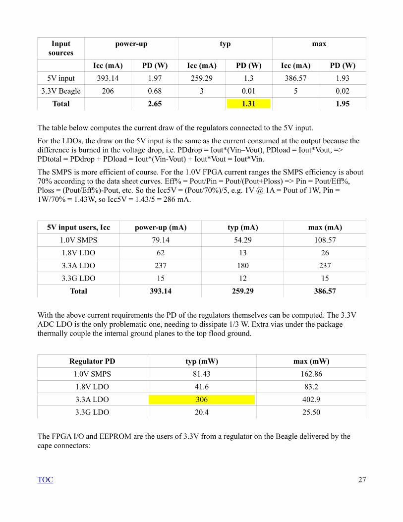
Inputsources
power-up typ max
Icc (mA) PD (W) Icc (mA) PD (W) Icc (mA) PD (W)
5V input 393.14 1.97 259.29 1.3 386.57 1.93
3.3V Beagle 206 0.68 3 0.01 5 0.02
Total 2.65 1.31 1.95
The table below computes the current draw of the regulators connected to the 5V input.
For the LDOs, the draw on the 5V input is the same as the current consumed at the output because the difference is burned in the voltage drop, i.e. PDdrop = Iout*(Vin–Vout), PDload = Iout*Vout, => PDtotal = PDdrop + PDload = Iout*(Vin-Vout) + Iout*Vout = Iout*Vin.
The SMPS is more efficient of course. For the 1.0V FPGA current ranges the SMPS efficiency is about 70% according to the data sheet curves. Eff% = Pout/Pin = Pout/(Pout+Ploss) => Pin = Pout/Eff%, Ploss = (Pout/Eff%)-Pout, etc. So the Icc5V = (Pout/70%)/5, e.g. 1V @ 1A = Pout of 1W, Pin = 1W/70% = 1.43W, so Icc5V = 1.43/5 = 286 mA.
5V input users, Icc power-up (mA) typ (mA) max (mA)
1.0V SMPS 79.14 54.29 108.57
1.8V LDO 62 13 26
3.3A LDO 237 180 237
3.3G LDO 15 12 15
Total 393.14 259.29 386.57
With the above current requirements the PD of the regulators themselves can be computed. The 3.3V ADC LDO is the only problematic one, needing to dissipate 1/3 W. Extra vias under the package thermally couple the internal ground planes to the top flood ground.
Regulator PD typ (mW) max (mW)
1.0V SMPS 81.43 162.86
1.8V LDO 41.6 83.2
3.3A LDO 306 402.9
3.3G LDO 20.4 25.50
The FPGA I/O and EEPROM are the users of 3.3V from a regulator on the Beagle delivered by the cape connectors:
TOC 27

3.3V input users, Icc power-up (mA) typ (mA) max (mA)
3.3V FPGA 205 2 4
EEPROM 1 1 1
Total 206 3 5
This table is the summary of the FPGA current consumption by supply voltage:
FPGA by supply, Icc power-up (mA) typ (mA) max (mA)
1.0V 277 190 380
1.8V 62 13 26
3.3V 205 2 4
There is a lot of uncertainty in the FPGA consumption until better constraints can be applied to the power analyzer. The numbers here are generated by setting the I/O pins to toggle at 100% of their respective clocking frequencies. In the absence of any simulation data the analyzer does static analysis to estimate the switching behavior of the internal nodes. It wouldn't be too difficult to guess at the behavior of some logic, e.g. most all the bits in the CIC filters will change every clock cycle. Most of the ADC lsbs will as well, etc.
For now the max column is simply set to twice the typ values.
The “power-up” column below is the minimum current required for proper power-up and configuration as specified by table 6 in the Artix-7 DC/AC Switching Characteristics.
FPGA power-up (mA) typ (mA) max (mA)
1.0V core 215 186 372
1.0V BRAM 62 4 8
1.8V aux 62 13 26
3.3V I/O banks 205 2 4
total 544 205 410
Typ and max Icc values are in the data sheets for all active parts except the typ of the clock driver which was not specified (max is pessimistically assumed).
TOC 28

3.3 ADC LDO Icc typ (mA) max (mA)
LTC6401-20 Op amp 50 62
LTC2248 ADC 68 80
XO 12 45
clock driver 50 50
Total 180 237
3.3 GPS LDO Icc typ (mA) max (mA)
SE4150L 10 13
TCXO 2 2
Total 12 15
TOC 29
6.7 Active AntennaThe design chosen is the PA0RDT Mini-Whip by Roelof Bakker, PA0RDT. It requires the fewest parts and has good performance. But the board also has pads and traces to support two Complementary Push-Pull Amplifier designs (figures 9 & 12) by Chris Trask, N7ZWY of Sonoran Radio Research. These designs offer improved second and third-order IMD performance. The user would just have to buy and solder-on (or remove) a number of SMD parts to switch designs. When a choice exists, larger SMD parts are used to ease this task (e.g. 0805/1206 resistors and caps).
Additional pads are provided for other options a user might want to experiment with:• A couple of inter-stage LC notch traps to reduce BCB station interference based on an inter-
stage HPF idea from VE7BPO.• an RLC LPF antenna input filter as described by Pieter-Tjerk de Boer, PA3FWM.• The ability to use a coax or CAT5 twisted-pair feed-line (W1TAG, PA0RDT/CARC, active-
antenna.eu LZ1AQ).
Questions:• Should the Trask Push-Pull be the default for a little extra money? (Survey says yes)
6.7.1 Version schematics
The active antenna and power injector schematics are confusing because all possible components have to be shown for the PCB layout creation. Many parts are marked do-not-load (DNL) or are populated with zero-ohm (0R) resistors as jumpers. Simplified schematics are shown below for each antenna version:
• Composite schematic• Simplified schematics for each configuration
6.7.2 Coupling bandwidth
When AC coupling is used between low impedance stages the layout provides for two capacitors in parallel. A combination of 470nF and 1nF should provide acceptable bandwidth from 10 kHz – 30 MHz (the -3 dB point of 470nF at 50Z is 6.8 kHz). I will probably have a test fabrication of the antenna/injector PCBs separately so the design can be validated. The Mini-Whip I'm using now is a simplified, hand-wired version.
6.7.3 Transistor selection
Several articles suggest the use of the relatively modern BFQ19 (NPN) and BFQ149 (PNP). But even the BFQ19 is now marked EOL from Infineon at both Mouser and DigiKey. The BFG35/31 are very similar in specifications to the BFQ19/149 and are packaged in a larger SOT-223 package, which will be helpful for users adding them at a later time for the Trask designs.
TOC 30

6.7.4 Power supply
Surprisingly, this was the most challenging aspect to design. The Vce max of the BFG31 is only 15V so the use of a voltage regulator on the active antenna board itself is required (the JFETs Vds are much higher). A TI TPS7A4501 in a SOT-223-6 package was chosen. It has a Vin max of 20V (which is enforced by the power injector regulator Vout of 16V minus feed-line drop), a low noise of 35 uVrms over standard bandwidth, reverse input polarity protection and the ability to dissipate the expected power. Some power dissipation in the antenna enclosure is actually good for helping limit condensation.
The output of the regulator is set to 14.55V (odd voltage due to limitations in values of 1% feedback resistors). As close as possible to the Vce max of the BFG31, with a safety factor, in the interest of best IMD. This part is a little pricey (~ $2.50) but more suitable parts from Linear Technology were much more expensive. First generation regulators all had too much noise or no noise spec at all.
6.7.5 Bias tee
This discussion applies to the bias tee portion of the power injector as well. Several sources, Clifton Labs Z1203B Power Coupler / DC Injector and Active Antenna DC Power Injector, suggest the choke portion of the bias tee consist of two series inductances to achieve sufficient frequency response from VLF – HF. No SMD part of reasonable size and cost is going to have really proper inductance for VLF. The values used are 100 uH and 2.0 mH. The latter is as large an inductance as possible with an acceptable size/cost and a 600 mA current limit. The 1K5 across the 100 uH is suggested in the Clifton Labs manual as a Q-spoiler for any self-resonance in the LC network.
6.7.6 Feed-line connection
Both single-ended coax and balanced CAT5 feed-lines are supported (coax is the delivered option). A simple screw-post terminal block for the connection of bare wires is used in addition to PCB pads for edge-launch BNC and SMA connectors.
CAT5 balanced line: An RJ-45 connector can be installed, or a second terminal block for connection of bare wires of a CAT5 cable. Pair assignments are as suggested by W1TAG resulting in a 50Z transmission line assuming the twisted pairs have a 100Z characteristic impedance. As shown in the configuration tables on the schematics T201/503 can be turned into common-mode chokes for the power pairs by changing some parts. Similarly, T203/504 are added as the balanced line transformers. The Mini-Circuits T1-6 used has a 3 dB response all the way down to 10 kHz.
TOC 31
6.7.7 Grounding
There are a number of grounding configurations possible and the user must experiment to find the one with the lowest noise. In my case I found the noise from the external 5V SMPS powering the Beagle, which was wiping-out reception on VLF/LF, could be completely eliminated by grounding the SDR to the outer braid of the coaxial CATV/satellite system. This noise was probably being coupled onto the outer braid of my active antenna feed-line and delivered to the antenna probe. This was confirmed as adding choke toroids to the feed-line reduced noise at other frequencies. Grounding to the AC system offered little improvement.
6.7.8 Enclosure
The width of the active antenna PCB has been sized to friction-fit inside a 40mm / 1-1/4in PVC pipe.
TOC 32

6.8 Active Antenna – Power Injector (bias tee)
It's difficult enough finding a quiet location for the active antenna and establishing a good ground connection to minimize noise. All of this can be undone by using a noisy power supply. For this reason it was decided that the user should supply a 12 Vac source to the power injector which will then do the conversion to DC in a hopefully quiet manner. The source will most likely be one of those AC adaptors with an integrated mains plug appropriate to the user's home country – nothing much more than a transformer and a fuse / PPTC.
Specs and tests show that an unloaded “12 Vac”, 0.05 – 2.0 A transformer actually delivers around 15 Vac rms. This is 42 Vac pk-pk so the components on the AC side of the bridge are appropriately voltage rated. After full wave rectification and filtering you get Vdc = Vac_rms*sqrt(2) – 2*diode_drop or around 20.5 Vdc max. Loading at 50 mA gives about 17.4 Vdc.
6.8.1 Filtering
An appropriately large DC filter cap (4700+ uF) is huge and likely only exists in a through-hole package. For DFM reasons I'm trying to avoid as many through-hole parts as possible. So I decided to use a scheme I found quite by accident and had not heard of before: the capacitance multiplier. A capacitor 10x smaller is used, 470 uF @ 35V, which has a 10x10 mm SMD footprint. Its effective capacitance is multiplied by the DC current gain (beta, h(FE)) of the associated transistor. For the MMBT4401 used (SMD version of 2N4401) the beta is roughly 100. One significant disadvantage in our case is the voltage drop through the transistor.
The multiplied capacitor, whatever its effective value, is followed by the largest inductance I could find in an SMD package (Bourns 20mH, 1A, 0.25R) with minimum series resistance which would otherwise cause even more voltage drop. This should form an LC LPF below 50/60 Hz to aid in removing powerline harmonics typically conducted through the mains connection.
6.8.2 Input protection
There wasn't an easy way to protect against input over-voltage from using too high of an AC supply (e.g. 15 or 18V instead of 12V). Some sort of crowbar circuit to trip the PPTC was judged too complex and expensive. The most likely mistake is someone using a DC supply. The bridge will let DC through of course. The LM2941 can withstand reverse polarity, but the filter cap would suffer. A possibility is saving the cap by adding a low-drop Schottky in the positive leg since this part is already used in the 1.0V switcher. The LM2941 has a Vin max of 60V and a typ Vin working max of 31V. A TVS is used to clip transients over 65V. A MOV was considered but they are relatively expensive.
6.8.3 Voltage & current distribution
There is a careful balance of active antenna power requirement, voltage regulator power dissipation and AC supply max/min conditions. A prototyped Mini-Whip draws about 1W. So the design goal for the TPS7A4501 output on the active antenna PCB is set at 3W (200mA @ 14.55V) to cover the Trask
TOC 33

designs with more active devices and for margin. The output of the LM2941 is set to 16V. The Vdropout max @ 500 mA of the TPS7A4501 is 250 mV. So this leaves 16 – 14.55 – 0.25 – 0.2 margin = 1V max of allowed feed-line voltage drop. The LM2941 Vdropout is similar so even if the AC source delivers exactly 12V (it should always be higher) then Vin will be sufficient.
At a Vin max of 16V the TPS7A4501 should dissipate 0.35Wmax. At a Vin max of 22V (16 Vac rms) the LM2941 should be 1.4W max. But at a nominal input of 15 Vac rms and 1.5W of delivered power the dissipations are less than half those amounts. The SOT-232-6 and TO-263 packages used by these parts both have ground connected to the package tab. At 1.4W the LM2941 needs about 4 square inches of PCB thermal ground plane to maintain a Tj of less than 100 deg C.
These assumptions need to be backed up with some actual measurements to characterize the various voltage drop sources. Similarly for the typical current consumption of the various active antenna configurations.
6.8.4 Diode noise
A paper from Dallas Lankford on Low Noise Active Antenna AC-DC Power Supplies demonstrates the need to bypass the individual diodes in a bridge rectifier because of the noise generated by their high speed switching. Further searching uncovers the whole complex topic of diode recovery characteristics and the generation of switching transients with subsequent LF/HF ringing due to interaction with transformer secondary leakage inductance and inter-winding parasitic capacitance (see Diode RecoveryEMI). Fancy diodes with ultra-fast recovery yet “soft” recovery profiles exist, but not at an acceptable price point. So the use of a snubber network on an inexpensive bridge rectifier is used.
6.8.5 Bias tee
See the discussion in the active antenna section. The option exists to configure T203 and R214 as a coax “braid breaker” in addition to its use as the CAT5 balanced line termination. It has been shown to give substantial noise improvement and will probably be the default PCB stuff option. By using a Mini Circuits T-622 at T203 a second receiver output is automatically available. Our prototyping has shown the T-622 has adaquate response down to 10 kHz.
TOC 34

6.9 Software
6.9.1 Source code
A snapshot of all the files is here on github. Everything is included: Beagle application code, Verilog, eCPU assembler, documentation and KiCAD files with schematic PDFs, Gerbers and the BOM post-processor.
6.9.2 Embedded CPU (eCPU)
We refer to the embedded CPU in the FPGA as the eCPU to distinguish it from CPU of the Beagle. The eCPU runs about 1000 lines of fairly simple assembly code. For the GPS it is mostly the slow part of the tracking demodulators. For the SDR the code mostly assists in the movement of data from FPGA registers and memory to the Beagle via the SPI. These tasks are more efficiently handled with sequential processing on a little eCPU than with logic gates. Since the eCPU is required for the GPS the SDR can use it basically for free.
I made some minor changes to the eCPU instruction set to accommodate the IO requirements of the SDR. The code memory space was doubled since that could be done almost for free (as Andrew's original design mentions). I wrote my own tiny macro assembler in C. This helps keep the eCPU code simple and the software distribution more self-contained, relying less on external tools. The assembler has some unique features. For example, a single header file of definitions (e.g. configuration parameters) is processed by the assembler and C/C++ compatible header files are automatically generated. Also generated are include files for the Verilog code. This is especially important since the Verilog code is heavily `ifdef'd so a limited-feature version can be easily configured for quicker synthesis.
6.9.3 Beagle application
The figure below gives an overview of the application software running on the Beagle. It can be run manually from the command line but the Makefile will also install a proper daemon so that the SDR is automatically started in the background when the Beagle is rebooted.
A tiny open-source web server called Mongoose is integrated directly into the code. This server does not listen on port 80 and so will not interfere with an existing web server running on the Beagle (port 8073 is the default). The usual web content is served including the user-interface HTML, Javascript and graphics files.
Mongoose also supports HTML5 WebSockets which is the mechanism used to transport streamed audio and waterfall data to the client browsers. Older browsers that do not support a recent version of HTML5 will simply not work. This is bound to make some people unhappy, but supporting the older methods of streaming data is just too difficult for this project. Fortunately HTML5 is now widely available.
There is no mobile-device version of the web interface at present.
TOC 35

The blocks labeled “audio” and “waterfall” contain the baseband processing of the decimated FPGA data. For audio this is bandpass filtering, AGC, demodulation and S-meter generation. For the waterfall it is the FFT and display processing. Most of the algorithms are from the open-source CuteSDR program by Moe Wheatley, AE4JY.
Efficient and predictable multi-threading is provided by a simple coroutine package in the original GPS code. I extended it to handle some additional features (priority levels, sleep/wakeup etc.) needed by the SDR.
A combination of C and C++ (GPS code) is used. The Makefile supports building on a development host (I use a Mac) for convenience and speed and on the Beagle itself under the Debian distribution. The FFTW and libconfig packages are the only third-party packages that must be installed and compiled against.
TOC 36

6.9.4 FPGA development
For the Artix-7 A35 the Xilinx Vivado WebPack tools must be used under Windows or Linux. I run Ubuntu Linux on my Mac via VirtualBox. Despite all these software layers Vivado runs reasonably well with this setup.
It was mentioned earlier that the Vivado IP core generators were used to define the DDS functions. This is also done for the DSP slices which are difficult to instantiate in Verilog directly (specifically carry in/out of adders for the GPS and eCPU).
TOC 37

6.9.5 Verilog
The Verilog code passes the Vivado timing and synchronization (clock domain crossing) checks. Timing constraints for all incoming clocks and I/O signals have been specified, specifically setup and hold requirements of the external interfaces (i.e. ADC, GPS, SPI).
6.9.6 Version checking, serial number
A unique serial number and PCB version ID will be stored in the EEPROM during board manufacture. The Verilog code is compiled with a version number that is checked at runtime against a similar version number in the application code. This prevents conditions where the application running on the Beagle is incompatible with the Verilog on the FPGA (a situation I encountered frequently during development when the code was changing rapidly).
TOC 38

7 PCBThe most important issues with the PCB design are:
• Minimizing noise coupling into the ADC and GPS front-ends.• Passing EMI/EMC regulatory testing.• Minimizing the manufacturing cost through DFM techniques.• Designing adequate FPGA power distribution.
7.1 BeagleBone cape compatibilityThe image below is a mostly complete KiCAD layout. The analog sections are on the left end with the front-end components under the RF shields.
The board deviates in two allowable ways from the Beagle SRM (section 8.0 “cape board support”):
7.1.1 PCB size
The board is currently 1.2 inches longer than a standard cape after the first attempt at placement and routing. This may be reduced although it is not clear the design would fit in a standard cape. At 4.6 x 2.2 inches the PCB is just below 10 square inches.
TOC 39

7.1.2 Beagle interface
The dual 46-pin (23x2) interface headers to the Beagle have been reduced (partially populated) to dual 26-pin (13x2) covering the power and interface signals actually used. The header change results in significant cost and board space savings. The 26-pin header with the non-standard long tail length is a part stocked by distributors, whereas the 46-pin is not.
7.2 Mixed-signal PCB designThere are several excellent articles about designing PCBs containing ADCs and FPGAs. The conclusions from those articles seem to be:
• Use a continuous ground plane common to the analog and digital circuit sections instead of two separate planes, single plane with slots, two planes connected under the ADC, two planes connected with inductors or ferrite beads, etc.
• In conjunction with the above, carefully partition the PCB space into analog, digital and power supply regions spaced as far apart as possible. The goal being to isolate the analog and digital return currents from each other.
• The ADC and GPS chips become the effective ground plane boundaries. Don't allow high-speed digital signals to cross onto the analog side.
• Never allow a digital signal to route without a decent return current path directly underneath as this immediately creates an RF loop that radiates.
• Don't overlap power planes and create coupling.• Use separate voltage regulators for the analog section(s).
7.2.1 General layout
The figure below shows the rough PCB layout using the above guidelines. The ADC and GPS front-end chips bridge to the digital section. The Beagle provides power and ground connections on the right end of the P9 header (top right). There are more ground pins on the left end of P8, and on the right end of P8, but my guess is that it's better to leave those unconnected and only use a single-point ground return path. On the board layout above the switching supply is at the upper right and the EEPROM at lower right.
TOC 40

TOC 41

7.2.2 RF shields
The shields being considered have a removable cover (BMI-S-209, page 14). Designing them in is probably essential to prevent problems with spurious signals getting into the ADC/GPS front-ends. The frames have a cross-support structure which can be cutout by the user to make component access easier if required.
7.2.3 GPS
This excellent GPS PCB design article goes into extensive detail. Be sure to click on the links for the figures which no longer appear in the article inline, especially this one. But the article contradicts the design rules given above for ADC/FPGA based system. The GPS design rules suggested are:
• Instead of a power plane use tracked RF power traces from the GPS LDO.
• Use an isolated ground plane that connects to the digital ground plane at the point where the digital signals leave.
• This is the most interesting one: Attach the RF shield can at a single point to the GPS ground plane through an inductor. This is apparently due to L1 frequency resonance considerations given the can dimensions (see article). You would ordinarily connect every tab of the shield can directly to the ground plane.
This advice seems pretty compelling. So I am using both sets of rules, opting to keep the continuous ground plane even for the GPS section.
7.2.4 ADC
I placed the ADC outside of the RF shield figuring it's better to route the low-impedance, differential output of the preamp a short distance outside rather than keeping the 14 ADC single-ended digital outputs inside. The outputs are routed on the top layer using no vias, connecting directly to some FPGA BGA outer-ring pads. Series resistors on the ADC end will be used to limit the edge rate and switching noise (value of 100R from page 3 of this article assuming 65 MHz sample clock and 15 pF worst case output loading). The trace lengths should be well under one inch.
7.2.5 Edge via stitching
Traditional via stitching every 5mm or so at the edges of the board is done to tie all the ground planes together and close the Faraday cages.
TOC 42

7.3 PCB specifications
7.3.1 Layer count
A six layer board makes routing of the FPGA power planes much easier compared to a 4 layer board. Six layers is certainly not needed for FPGA signal routing escape with such a simple design. My assumption is that the cost differential in a medium production run, say Q100, isn't going to be that great.
7.3.2 Surface finish
ENIG or equivalent will be specified to get the surface flatness required by the BGA and QFN packages.
7.3.3 PCB stackup
Below is a representation of the 6 layer stackup. 1.6mm / 63mil is a standard thickness for a six layer board and is required by the edge-mount SMA/BNC connectors.
TOC 43

7.3.4 Layer assignment
The layer assignment is pretty standard. Primary signals, including all analog, are on the top layer for accessibility. A ground pour on the top layer is also used. These two choices will minimize the number of signal and ground vias, hence drill hits, required.
The primary ground plane on layer two provides a continuous ground plane and allows for the GPS co-planar waveguide mentioned below.
The primary power planes, 3.3V digital, 3.3V ADC, 3.3V GPS and 1.8V FPGA are on layer three in non-overlapping regions.
Layer four is another continuous ground plane and should help isolate the overlapping power planes of layers three and five.
Layer five has the 1.0V FPGA plane which would otherwise be difficult to route along with the other FPGA power planes on a four layer board. The 5V input power plane to all the regulators is on this layer.
Layer six on the bottom has a few signal traces but mostly accommodates the smaller FPGA bypass caps. It also has a flood ground plane like the top layer.
On the power layers a ground plane fills-in the places where there is no power plane.
7.3.5 Controlled impedance
The GPS antenna connection runs at L1 (i.e. the active antenna doesn't down-convert) and so requires a 50Z trace. A grounded co-planar waveguide design is used because I read someplace that it is slightly less lossy than a microstrip line. KiCAD has a built-in calculator for these so it is simple to adjust the waveguide dimensions for the particular dielectric constant specified by the PCB house.
7.4 Layout design rules
7.4.1 Unit choice and layout grid
I decided to use metric units for the board and footprints.
The smaller parts are centered on a 0.25mm grid and a 1.0mm grid is used for larger parts. Adjustments smaller than 0.25mm are of course made where necessary for precise alignment.
7.4.2 Traces and vias
This table shows the design rules chosen for traces and vias. Mil (0.001in) equivalents are shown because most of us are used to this unit for trace and drill sizes.
The BGA ball pad and escape via sizes are Xilinx recommended for the FPGA FTG256 package. That package has 1.0mm ball pitch.
The same 0.6/0.3mm via/drill combo is used as the general signal via size to avoid adding another drill size to the design. Whether this really saves any cost will have to be verified with the PCB vendor. Some online quote systems charge a premium for small drill hits.
TOC 44

A 6/6mil trace is required for a single trace between ball pads to escape the BGA on the top layer. This signal density is fine for this relatively simple design. No need for trying to cram two traces between pads. There are a few FPGA signal traces on the bottom layer.
The general signal traces are 8/8mil which should help keep fab costs low. With a little work it wouldn't be hard to increase this to 10mil if necessary.
Power & ground traces are 12mil with a 0.8/0.4mm via. These traces are mostly used to tie a power-related 0402 pad to a via. The 0.3mm width is slightly less than the 0.4mm short-side of the pad. Except for the 3.3V GPS rail most power distribution is done with a plane and not these relative narrow traces.
designrules
trace width/clearance via pad diameter drill diameter
mm mil mm mil mm mil
BGA pad - - 0.400 15.7 - -
FPGA escape 0.150 6 0.600 23.6 0.300 11.8
generalsignal
0.200 8 0.600 23.6 0.300 11.8
power / gndtraces
0.300 11.8 0.800 31.5 0.400 15.7
7.4.3 SMD pad connection to planes
There is some disagreement on the web about whether SMD pads should have thermal or solid connections to planes, e.g. flood ground planes on the top layer or a localized top plane in a low-inductance environment like a SMPS. Some people say the pre-heat cycle of a reflow oven heats the planes sufficiently to prevent problems compared to wave soldering. Others, mostly PCB assemblers, say for volume production you're always going to have tombstoning and shifting/twisting problems if there is a differential in the amount of copper connected to the pads.
Currently the design uses thermal pads with a 0.2mm spoke width. But converting to a solid connection is a global zone setting in KiCAD and easy to change.
Questions:
• Your opinion / experience?
7.4.4 Planes / zones
All planes are pulled-back 0.5mm from the board edges.
KiCAD allows all the parameters of zone construction to be specified so it's fairly easy to fine-tune the result.
TOC 45

7.5 Other PCB elements
7.5.1 Fiducials
Standard 1mm fiducials, with a 3mm diameter soldermask-free area, are used. Two are at opposing corners of the FPGA to aid placement alignment, although these days placing a 1mm pitch BGA doesn't seem to be much of a challenge for most assemblers. Another global fiducial is at the board corner opposite the FPGA for board registration.
7.5.2 Tooling holes
There are four 0.125in tooling holes at the corners of the board. The two that overlap the standard Beagle footprint align with the holes on the Beagle so that rigid attachment with board spacers is possible. These holes are not plated because I don't want to introduce other ground paths if metallic spacers are used. Also I read someplace that tooling holes aren't supposed to be plated for alignment accuracy reasons (interestingly, the Beagle holes are plated). Tooling holes are used for registration during electrical testing and other operations.
7.5.3 Panelization
The details of panelization won't be decided until a particular PCB vendor is chosen. It seems some prefer to do it for you and others not. There are more considerations if the active antenna is included with each SDR built.
7.5.4 Edge keepout
There are no SMD components placed within 1.5mm of the board edge.
7.5.5 Test pads
Test pad connection and placement is still being considered as there is not a specific test plan yet. I have defined some test pad footprints. The usual top and bottom layer pads that can be placed inline with a trace or connected to separately. And footprints that look like vias except that the top or bottom pad is not tented. This allows, for example, a test pad to appear on the bottom layer that is directly connected with the via hole to a trace underneath the BGA.
7.5.6 Layer ID
The usual numeric layer ID strip is included at one board corner.
7.6 Thermal / RF ground via-in-padThis is a gigantic controversy I knew nothing about until recently. Fortunately there is plenty of excellent material on the web about the problem. It occurs because of modern QFN / QFP packages that contain a bottom leadframe die pad that wants to be connected with in-pad vias to as many ground layers as possible for thermal and/or RF grounding reasons (e.g. TI PowerPAD).
TOC 46

The primary problem is how to keep the via holes from wicking the solder off the pad during reflow.
Via-in-pad is needed for many of the active parts:
• GPS front-end, RF grounding
• ADC preamp, RF grounding, heat dissipation
• ADC, RF grounding, heat dissipation
• 1.0V SMPS, heat dissipation
7.6.1 Existing solutions
There are a number of solutions:
• Filled and plated vias. Fill the via holes with epoxy and plate over them. Expensive.
• Tiny vias. Use via holes that are < 0.33mm / 13mil which should reduce the capillary action.
• Tented vias, top and/or bottom. Get your CAD program to somehow tent the vias in the pads.
• Selective solder mask and solder paste strips/squares. Since the pad is relatively large the stencil is generally segmented into small squares to limit the amount of paste applied. With this scheme solder mask is used outside the stencil areas and the vias placed there where they will be covered.
7.6.2 KiCAD footprint solution
In KiCAD I could not find any combination of footprint settings to produce tented vias in a pad. But I did find a way to do “mask/paste strips”. Below are images from Gerbv.
Copper + holes:
TOC 47

Add silkscreen [white/blue].
Add paste [grey]. So the via holes end up under silkscreen and hopefully tented.
Questions:
Anyone have experience with the via-in-pad issue?
7.7 FPGA BGA issues
7.7.1 Power planes
As mentioned earlier a 6 layer board makes FPGA power plane routing much easier. Below is layer 5 showing how the 1.0V core power (dogleg) enters from the SMPS on the right. The surrounding zone is the 5V input plane (the vertical blue lines seem to zone-filling artifacts from the particular version of KiCAD I'm running – they don't appear in the Gerbers).
TOC 48

Below is layer 3 showing the 1.8V aux plane in the middle to the LDO on the right. The surrounding zone is the 3.3V digital plane.
TOC 49

7.7.2 Traces and vias
As mentioned earlier 0.150mm / 6mil traces are used on the top layer under the BGA to clear the 0.400mm ball pads. These traces transition to the standard 0.200mm / 8mil signal traces at the BGA edges.
The minimum clearance between any ball pad, via and trace combination is 0.150mm / 6mil. Gerber of top layer:
TOC 50
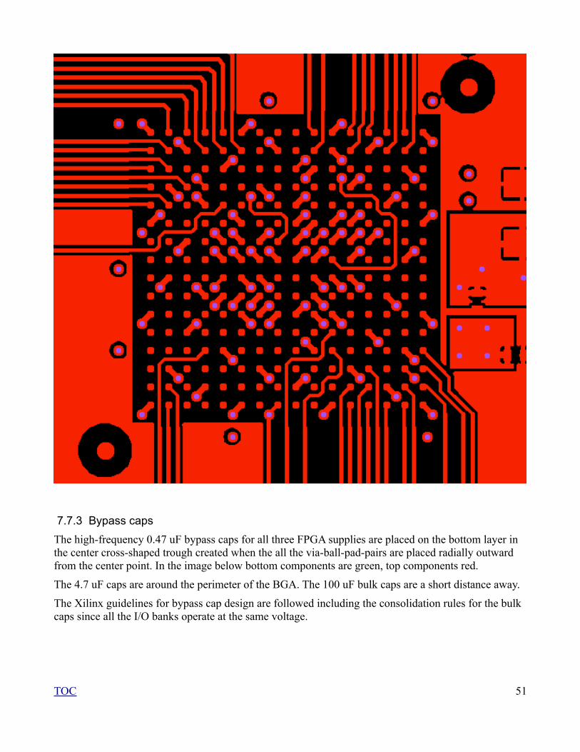
7.7.3 Bypass caps
The high-frequency 0.47 uF bypass caps for all three FPGA supplies are placed on the bottom layer in the center cross-shaped trough created when the all the via-ball-pad-pairs are placed radially outward from the center point. In the image below bottom components are green, top components red.
The 4.7 uF caps are around the perimeter of the BGA. The 100 uF bulk caps are a short distance away.
The Xilinx guidelines for bypass cap design are followed including the consolidation rules for the bulk caps since all the I/O banks operate at the same voltage.
TOC 51

TOC 52
8 EMC / EMI
8.1.1 Proximity to Beagle
Having an SDR in such close proximity to the Beagle is a concern. But there are a few issues that can be mitigated.
The SDR and GPS front-ends are purposely placed on the end of the board furthest from the Beagle SMPS and processor.
The HDMI port on the Beagle can be turned off. This is important since the HDMI framer chip and connector are at the end of the Beagle closest to our front-ends. Note this is not a concern on the new lower-cost BeagleBone Green which doesn't include the HDMI framer.
8.1.2 SMPS switching transient propagation
I'm actually more worried about EMI from the external 5V SMPS which connects to the ADC / GPS LDOs than the on-board FPGA 1.0V SMPS. A two-stage output filter could be added to the 1.0V SMPS if needed. Including one of those large snap-on ferrite cable chokes in the product for the user to apply to the external 5V supply cable is a possibility.
8.1.3 Clock harmonics within the GPS L1 bandwidth
Experience with the hand-wired prototype shows that the GPS front-end is very sensitive to clock harmonics that land within the ~2 MHz L1 bandwidth.
Our ADC clock should be okay. A 65.36 MHz ADC clock 24th harmonic is 6.8 MHz below L1. A 65 MHz clock (a more likely value to be used in production) 24th harmonic is 15.4 MHz below. The 25th harmonics are roughly 50 MHz above.
As for Beagle clock harmonics the GPS on the hand-wired prototype worked fine as long as the ADC clock was off. In that prototype the ADC clock was derived from 4x the GPS TCXO, so the harmonics landed at the GPS IF offset of 4.092 MHz. So the Beagle clocks didn't seem to be a problem.
All the clock frequencies are listed in the Beagle's FCC test report. The only problem is the 63rd harmonic of the 25 MHz Ethernet PHY clock which lands 420 kHz below L1. But this clock doesn't go anywhere else on the board. My hand-wired prototype uses 100 Mb/s Ethernet as the Beagle network connection as opposed to USB or WiFi.
As more verification, all the peak response listed in the Beagle's radiated emissions test (below) were checked. The 7th harmonic of that 228 MHz response is 20 MHz above L1. The others were at least 45 MHz away with most many hundreds of MHz.
TOC 53

8.1.4 Certification
I have no experience obtaining agency approvals. Having access to the full Beagle test report is extremely useful. The main issues seem to be:
• Which agency approvals?
◦ FCC
◦ CE
◦ For other world destinations, e.g. RCM for AUS / NZ
• Which documentation processes?
◦ REACH (RoHS)
• Logistics
TOC 54

Do you personally have to visit the test house to do the setup or apply fixes during testing? I have a good spectrum analyzer and could buy a cheap near-field E-probe to at least check for overly hot narrowband (clock) problems.
• Cost
I'm guessing $5k - $25k depending on the number of tests required and testing iterations. This is a major reason for doing a Kickstarter I think.
Questions:
Your advice and experience is most welcome.
TOC 55

9 DFMThis section lists design-for-manufacturing issues some of which were partially discussed earlier.
9.1 Parts commonalityWhere possible part value and packages have been consolidated to reduce the number of simultaneous reels / tubes needed on the pick-and-place machine. Too many parts might otherwise require multiple placement runs. For example, in a few cases bypass cap values were altered to eliminate adding another unique BOM item. This helps increase the item purchase quantity as well.
9.2 Minimizing high assembly-cost parts
9.2.1 Through hole
Through-hole parts are minimized but cannot be totally eliminated. There are SMD versions of the cape headers but right angle alignment is critical for proper mating with the Beagle connectors. So the proven through-hole solution will be used. But this has other problems (see below).
The antenna terminal block also has an SMD version, but it is very expensive. The least expensive of the SMD choices doesn't have a good mechanical attachment footprint to the board.
9.2.2 Fine pitch
Fine pitch being defined as <= 0.5mm. These type of parts usually incur an extra assembly charge. There are 6 of these parts on the board:
• ADC op amp
• ADC
• GPS
• SMPS
• 2x 100R resistor networks
9.3 Placement spacingThe spacing between components is fairly loose given the larger board size. Some references about component spacing were found on the net but seemed dated. For any board shrink the PCB vendor will be consulted in advance for their placement capabilities.
9.4 BGA inspection clearanceThere is at least 1.0mm of inspection clearance around the BGA.
TOC 56

9.5 QFN pad pullbackAll QFN pads have enough pullback from the package boundary to inspect the solder fillet and aid probing.
9.6 Copper warping / twisting during reflowWe avoid any large areas of no copper on any layer which might cause uneven board heating during reflow. For example, on the internal power planes filling in the unused areas with a ground plane and using flood ground planes on the top and bottom layers.
9.7 SMD tombstoning / shiftingAs mentioned earlier we might prefer to switch the SMD pad-to-zone connections from thermal to solid in the interest of less connection inductance, but only if this doesn't cause tombstoning / shifting problems. This might also be done selectively in places where it is of more consequence (e.g. SMPS).
Trace exits from the 0402 pads have balanced geometry where possible so the surface tension pull is equal. This is probably more important with the 0.300mm power / gnd trace width.
9.8 Reverse header solderingIt's bad enough that the cape header connector is a through-hole part. But it's really annoying that it has to be reverse soldered. That is, the header is installed through the bottom of the board and soldered on the top layer, so the long pins of the header point downward. Example:
TOC 57

I've seen a process called “spot soldering” that seems to address this problem. The assembly house got this wrong on the first PCBs I had built.
9.9 Test methodologyThere is no specific test methodology yet, but the attached Beagle is almost a test fixture in itself (I have done this on another project where there was an integrated Beagle). The four Beagle LEDs can be overridden to communicate an error code.
9.9.1 RF source
To test the RF chain and ADC it's likely a simple external signal source will have to be connected.
9.9.2 JTAG
The four FPGA JTAG signals are connected to test pads and Beagle GPIOs. JTAG is not needed for FPGA configuration as the simpler slave SPI mode is used. But JTAG is useful for manufacturing test of the FPGA I/O traces.
TOC 58

10 Bill of MaterialsThe bill-of-materials is generated from BOM information output by KiCAD post-processed by a small custom C program. The program adds manufacturer and part number information based on matching value/package info from the KiCAD BOM. In this way you can change most parts without having to re-annotate fields in the schematic.The resulting BOM .csv file is then uploaded to octopart.com for quotation which produces another .csv file which is downloaded. The same custom program then breaks the quote into design categories for analysis and double-checking. Statistics are also produced for the online PCB fab quotation sites, e.g. total number of SMD pads, # of fine-pitch parts (< 0.5mm), # of through-hole parts, # of no-lead parts, # of manually placed parts (e.g. connectors), etc.
Currently, if you include the active antenna, there are 200 instances of 70 unique parts (150 of 50 for just the SDR). A build of 100 units quotes as US$100 (less PCB and assembly costs). 1000 units is $90. 10 is $120. The FPGA and ADC are about $30 each. 83% of the cost is the receiver, 7% the GPS and 10% the active antenna.
Of course the actual costs of getting real boards made will be different. Assembly houses have a certain amount of markup if they are to procure parts. And for large or ongoing builds it pays to develop a relationship with the inside-sales group of component suppliers rather than going through distributors.
Differing values of jellybean parts (caps etc.) were minimized in the design to lessen the number of reels required on the pick-and-place machines for DFM reasons (lesser setup charges hopefully).
You can quote the design with octopart, or another service, as follows. Download the BOM .csv file to your computer. Goto the the octopart.com website and click “upload BOM” and specify the file you just downloaded. Set “[column 5]” as the part number field and “[column 2]” as the quantity. In the optional “line item details” you could set the description column to “[column 3]” which is the part value. With the edit option on “Selected Distributors” add Avnet Express to the existing list of Digi-Key, Mouser and Newark. Set the batch size to 100. Finally, set the drop-down menu to “Lowest Price (Selected)”. You should get a quote of around $100 with 100% BOM coverage.
Using “Lowest Price (Selected)” is a way of quoting from a small set of distributors as opposed to quoting the cheapest price from every single distributor in Octopart's database (you'd never order this way during production. Avnet Express currently has the best quantity prices on the FPGA. Mouser beats DigiKey as usual, but doesn't carry everything including Linear Technology. Newark beats them both, but doesn't always have stock or the particular part.
TOC 59

11 Schematics and Files
• All files on Github
• Schematics, all sheets
• Active antenna, simplified schematics
• KiCAD gerbers, drill files, .tar
• BOM ODS, BOM XLS
TOC 60

12 RisksThere are a number of design risks, of different probabilities and importance. Some already have good mitigation.
• Untraceable source of high noise-floor or spurs (biggest worry)• Production costs are too high at needed volumes for acceptable price point (very likely)• Excessive thermal dissipation (possibly in the 3.3V ADC regulator)• Insufficient FPGA power supply current (maybe for some applications)• FPGA ultimately too small to fit all needed logic (unlikely)• SPI bandwidth or throughput insufficient (possible, hence expansion port)• Unfixable Linux latency causes audio stream stuttering (possible)• With the full four users the waterfall update rate becomes too slow (is now reasonable)• Can't properly derive timing from GPS-SDR code (seems okay)• Clock harmonics within GPS L1 bandwidth causing self-jamming (seems okay)• Design is unable to pass type-acceptance testing (always an issue)• Parts obsolescence or acquisition issues (always an issue)• Low cost ADC becomes unavailable (possible)• Attack by angry pitchfork-wielding Kickstarter backers
Questions:Surely you have something to add to this list.
TOC 61

13 Abbreviations
0R zero ohm resistor, i.e. jumper
ADC Analog-to-Digital converter
AGC Automatic Gain Control
BCB AM Broadcast Band (~ 530 – 1710 KHz)
BGA Ball Grid Array, chip package
BNC connector type
BOM Bill of Materials, list of parts and their specifications
BRAM Block RAM, type of bulk FPGA memory
C/A GPS Coarse Acquisition code
C / C++ computer programming languages
CAD Computer Aided Design
CAT5 Category 5, twisted-pair (4) Ethernet cable, nominal pair Z = 100 ohms
CATV Cable Television
CIC Cascaded Integrator-Comb filter, type of high performance digital lowpass filter
CORDIC COordinate Rotation DIgital Computer
CPU Central Processing Unit
DDC Digital Down Converter (Conversion), mixing and decimation technique
DDS Direct Digital Synthesis
DFM Design for Manufacturing
DMA Direct Memory Access
DNL Do Not Load, aka Do Not Place (DNP), No Load (NL)
DSP Digital Signal Processing
EEPROM Electrically Erasable Programmable Read-only Memory
EFC Electronic Frequency Control
EMC Electro-Magnetic Compatibility
EMI Electro-Magnetic Interference
eMMC Embedded MultiMediaCard, Beagle file system storage
ENIG Electroless Nickel Immersion Gold, PCB plating technique
EOL End of Life (parts no longer manufactured, subject to existing stock)
F connector type
TOC 62

FE Front End, typically analog
FFT Fast Fourier Transform
FIFO First-In-First-Out, type of memory organization
FIR Finite Impulse Response, filter type
FLL Frequency-locked loop, control loop that adjusts frequency but not necessarily phase (as does a PLL)
FPGA Field Programmable Gate Array
GDT Gas Discharge Tube
GE Gigabit Ethernet
GPIO General Purpose Input/Output
GPS Global Positioning System
GPSDO GPS Disciplined Oscillator
HDMI High-Definition Multimedia Interface, video interface standard
HF High Frequency, 3 – 30 MHz
HPF High-Pass Filter
I2C I-two-C, aka IIC, serial interface
IMD Inter-modulation Distortion
IP Intellectual Property, also Internet Protocol
IQ, I/Q In-phase Quadrature, modulation and data transmission technique
L1 base GPS operating frequency, 1575.42 MHz
LC Inductor – Capacitor network
LDO Low Dropout Regulator
LPF Low-pass Filter
lsb Least Significant Bit
LTC Linear Technology Corporation
LVDS Low Voltage Differential Signalling
LF Low Frequency, 30 – 300 KHz
LW Longwave, historical term, generally VLF & LF and sometimes part of MF
MAC Media Access Controller, e.g. Ethernet controller
MF Medium Frequency, 300 KHz – 3 MHz
MISO Master-In / Slave-Out, SPI data signal
mmap() memory map, Unix mechanism to map devices into user address space
MOSI Master-Out / Slave-In, SPI data signal
TOC 63

MOV Metal-Oxide Varistor, transient suppressor
msb Most Significant Bit
MSPS Mega Samples Per Second
NAND Flash memory architecture
NCO Numerically-Controlled Oscillator
PCB Printed Circuit Board
PD Power Dissipation
PHY Physical transceiver, Ethernet
PLL Phase Locked Loop
PMIC Power Management Integrated Circuit
PPS Pulse Per Second, typical GPS receiver output
PPTC Polymeric PTC (aka Polyfuse), automatically resettable over-current fuse
PRU Programmable Realtime Unit, Beagle TI Sitara CPU on-chip co-processors (2)
PSK Phase Shift Keying
PSRR Power Supply Rejection Ratio
QFN Quad Flat No-leads, chip package
QFP Quad Flat Package, chip package
RBW Resolution Bandwidth, frequency bandwidth of one FFT display pixel
RJ45 connector type used for twisted-pair Ethernet
RLC Resistor – Inductor – Capacitor network
RoHS Restriction (Reduction) of Hazardous Substances, aka Lead-Free
SD-GPS Software-defined GPS, implemented in FPGA and host software
SDR Software-defined Receiver
SFDR Spurious-Free Dynamic Range
SMA connector type
SMD Surface Mount Device
SMPS Switched (switching) -Mode Power Supply
SNR Signal-to-Noise Ratio
SPI Serial Peripheral Interface
SRAM Static Random Access Memory
SRM System Reference Manual
TCXO Temperature-Compensated Crystal Oscillator
TVS Transient Voltage Suppressor
TOC 64

USB Universal Serial Bus
uSD MicroSD card
XO Crystal Oscillator
VLF Very Low Frequency, 3 – 30 KHz
WSON tiny chip package type
WSPR Weak Signal Propagation Reporter
XOR Exclusive-OR
TOC 65