Keysight Technologies Designing and Testing 3GPP W-CDMA Base ...
64
Keysight Technologies Designing and Testing 3GPP W-CDMA Base Transceiver Stations (Including Femtocells) S - P OVSF code generator I Q Complex scramble code generator Q I + + + - Spreading Q scramble I scramble I scramble DPCCH Time multiplexer CCTrCH Complex scrambling Add CRC & tail bits DTCH data bits Add CRC & tail bits DCCH data bits Conv. coder Conv. coder Rate matching Rate matching Interleaver Interleaver Frame segment Frame segment TrCH mux Interleaver Application Note
Transcript of Keysight Technologies Designing and Testing 3GPP W-CDMA Base ...
Keysight TechnologiesDesigning and Testing 3GPP W-CDMA Base Transceiver Stations(Including Femtocells)
S - POVSFcode
generator
I
Q
Complexscramble code
generator
Q
I+
+
+
-
Spreading
Q scramble
I scramble
I scramble
DPCCH
Time multiplexer
CCTrCH
Complexscrambling
Add CRC &tail bits
DTCHdata bits
Add CRC &tail bits
DCCHdata bits Conv. coder
Conv. coder Ratematching
Ratematching
Interleaver
Interleaver
Framesegment
Framesegment
TrCHmux Interleaver
Application Note
Table of Contents
Introduction . . . . . . . . . . . . . . . . . . . . . . . . . . . . . . . . . . . . . . . . . . . . . . . . . . . . . . . . . . . . . . . . . . . . . . . . 31 . Basic Concepts of W-CDMA . . . . . . . . . . . . . . . . . . . . . . . . . . . . . . . . . . . . . . . . . . . . . . . . . . . . . . . 4 1 .1 Code division multiple access . . . . . . . . . . . . . . . . . . . . . . . . . . . . . . . . . . . . . . . . . . . . . . . . 4 1 .2 Base transceiver station and user equipment identification . . . . . . . . . . . . . . . . . . . . . . . 5 1 .3 Data channelization . . . . . . . . . . . . . . . . . . . . . . . . . . . . . . . . . . . . . . . . . . . . . . . . . . . . . . . 5 1 .4 Slots, frames, and power control . . . . . . . . . . . . . . . . . . . . . . . . . . . . . . . . . . . . . . . . . . . . . . 7 1 .5 Protocol structure . . . . . . . . . . . . . . . . . . . . . . . . . . . . . . . . . . . . . . . . . . . . . . . . . . . . . . . . . 7 1 .6 Logical, transport, and physical channels . . . . . . . . . . . . . . . . . . . . . . . . . . . . . . . . . . . . . . 8 1 .7 Downlink physical channels . . . . . . . . . . . . . . . . . . . . . . . . . . . . . . . . . . . . . . . . . . . . . . . . . 9 1 .8 Uplink physical channels . . . . . . . . . . . . . . . . . . . . . . . . . . . . . . . . . . . . . . . . . . . . . . . . . . . 11 1 .9 Transport format detection . . . . . . . . . . . . . . . . . . . . . . . . . . . . . . . . . . . . . . . . . . . . . . . . . . 14 1 .10 Downlink DPDCH/DPCCH coding and air interface . . . . . . . . . . . . . . . . . . . . . . . . . . . . . .15 1 .11 Uplink DPDCH/DPCCH coding and air interface . . . . . . . . . . . . . . . . . . . . . . . . . . . . . . . . 16 1 .12 Test models and reference measurement channels . . . . . . . . . . . . . . . . . . . . . . . . . . . . . 17 1 .13 Fixed reference measurement channels . . . . . . . . . . . . . . . . . . . . . . . . . . . . . . . . . . . . . . 18 1 .14 Compressed mode . . . . . . . . . . . . . . . . . . . . . . . . . . . . . . . . . . . . . . . . . . . . . . . . . . . . . . . . . 18 1 .15 Asynchronous cell site acquisition . . . . . . . . . . . . . . . . . . . . . . . . . . . . . . . . . . . . . . . . . . . 18 1 .16 Asynchronous cell site soft handover . . . . . . . . . . . . . . . . . . . . . . . . . . . . . . . . . . . . . . . . 19 2 . General Design and Measurement Issues . . . . . . . . . . . . . . . . . . . . . . . . . . . . . . . . . . . . . . . . . . 20 2 .1 Controlling interference . . . . . . . . . . . . . . . . . . . . . . . . . . . . . . . . . . . . . . . . . . . . . . . . . . . . 20 2 .1 .1 Average RF power . . . . . . . . . . . . . . . . . . . . . . . . . . . . . . . . . . . . . . . . . . . . . . . . . . 21 2 .1 .2 Adjacent channel interference . . . . . . . . . . . . . . . . . . . . . . . . . . . . . . . . . . . . . . . . 22 2 .2 Handling high peak-to-average power ratios . . . . . . . . . . . . . . . . . . . . . . . . . . . . . . . . . . . 23 2 .2 .1 Complementary cumulative distribution function . . . . . . . . . . . . . . . . . . . . . . . . . . . 24 2 .3 Measuring modulation quality . . . . . . . . . . . . . . . . . . . . . . . . . . . . . . . . . . . . . . . . . . . . . . . 26 2 .3 .1 QPSK EVM . . . . . . . . . . . . . . . . . . . . . . . . . . . . . . . . . . . . . . . . . . . . . . . . . . . . . . . . . 27 2 .3 .2 Composite EVM . . . . . . . . . . . . . . . . . . . . . . . . . . . . . . . . . . . . . . . . . . . . . . . . . . . . . . 29 2 .3 .3 Code domain power . . . . . . . . . . . . . . . . . . . . . . . . . . . . . . . . . . . . . . . . . . . . . . . . . . 31 2 .3 .4 Peak code domain error . . . . . . . . . . . . . . . . . . . . . . . . . . . . . . . . . . . . . . . . . . . . . . . 33 2 .3 .5 Symbol EVM . . . . . . . . . . . . . . . . . . . . . . . . . . . . . . . . . . . . . . . . . . . . . . . . . . . . . . . . 34 2 .3 .6 Symbol power versus time . . . . . . . . . . . . . . . . . . . . . . . . . . . . . . . . . . . . . . . . . . . . . 36 2 .3 .7 Demodulated bits . . . . . . . . . . . . . . . . . . . . . . . . . . . . . . . . . . . . . . . . . . . . . . . . . . . . 37 2 .3 .8 Power control in the downlink . . . . . . . . . . . . . . . . . . . . . . . . . . . . . . . . . . . . . . . . . . 38 2 .4 Measuring receiver performance . . . . . . . . . . . . . . . . . . . . . . . . . . . . . . . . . . . . . . . . . . . . . . . 39 2 .4 .1 Bit error rate (BER) versus block error rate (BLER) . . . . . . . . . . . . . . . . . . . . . . . . . . 40 2 .4 .2 Stimulus signals for receiver characteristics and performance tests . . . . . . . . . . . . . . . . . . . . . . . . . . . . . . . . . . . . . . . . . . . . . . . . . . . 42 2 .4 .3 Verification of internal BER and internal BLER calculation . . . . . . . . . . . . . . . . . . . 44 2 .4 .4 Verifying RF performance . . . . . . . . . . . . . . . . . . . . . . . . . . . . . . . . . . . . . . . . . . . . . . . 44 2 .4 .5 Verifying baseband functionality . . . . . . . . . . . . . . . . . . . . . . . . . . . . . . . . . . . . . . . . . 45 2 .4 .6 Verification of compressed mode functionality . . . . . . . . . . . . . . . . . . . . . . . . . . . . . 45 2 .4 .7 Verification of PRACH reception . . . . . . . . . . . . . . . . . . . . . . . . . . . . . . . . . . . . . . . . . 46 2 .4 .8 Verification of uplink power control . . . . . . . . . . . . . . . . . . . . . . . . . . . . . . . . . . . . . . .47 3 . Special Considerations for Femtocells . . . . . . . . . . . . . . . . . . . . . . . . . . . . . . . . . . . . . . . . . . . . . 48 3 .1 Additional test requirements for GPS-enabled femtocells . . . . . . . . . . . . . . . . . . . . . . 49Summary . . . . . . . . . . . . . . . . . . . . . . . . . . . . . . . . . . . . . . . . . . . . . . . . . . . . . . . . . . . . . . . . . . . . . . . . 49Appendix A: Conformance Test Setup Tables . . . . . . . . . . . . . . . . . . . . . . . . . . . . . . . . . . . . . . . . . . . . 50Appendix B: Keysight Solutions for W-CDMA BTS Design and Test . . . . . . . . . . . . . . . . . . . . . . . . . . 52Acronym Glossary . . . . . . . . . . . . . . . . . . . . . . . . . . . . . . . . . . . . . . . . . . . . . . . . . . . . . . . . . . . . . . . . . . 62References . . . . . . . . . . . . . . . . . . . . . . . . . . . . . . . . . . . . . . . . . . . . . . . . . . . . . . . . . . . . . . . . . . . . . . . . 63Related Literature . . . . . . . . . . . . . . . . . . . . . . . . . . . . . . . . . . . . . . . . . . . . . . . . . . . . . . . . . . . . . . . . . . . 63
2
Introduction
W-CDMA is the leading wideband digital cellular technology used for the third generation (3G) cellular market .
The Third Generation Partnership Project (3GPP) system employs wideband CDMA in both frequency division duplex (FDD) and time division duplex (TDD) modes . To limit its scope, this application note focuses on the FDD mode of W-CDMA, although most of the content is applicable to both modes . Whenever the term W-CDMA is used throughout the application note it is in reference to the 3GPP (Release 99) specifications for W-CDMA FDD mode . Specific reference to later releases of the specifications are made when appropriate .
This application note focuses on the physical layer (layer 1) aspects of W-CDMA base trans-ceiver stations (BTS) . It consists of
– a brief overview of W-CDMA technology – a discussion of design issues and measurement concepts related to the technology that are important for the W-CDMA BTS air interface because of the differences between W- CDMA and its second generation (2G) predecessors (specifically the Global System for Mobile Communication (GSM)) . This section will provide you with an understanding of why these measurements are important and how you can use them to characterize and troubleshoot designs . These measurements can be useful throughout the development of the BTS . This section can also be used as back-ground information for conformance tests .
– a discussion on the specific requirements of a new class of base station that has recently emerged — the femtocell . Femtocells (3GPP Home Node B for W-CDMA/ HSPA) are low-power wireless access points that connect standard mobile devices to a mobile operator’s network via residential DSL or cable broadband . While a compelling entrant into the broadband CPE (Consumer Premises Equipment) market dominated by Wireless LANs, femtocells are forcing manufacturers to confront a number of new test considerations . Since they operate in the licensed spectrum, they face the same stringent conformance requirements as normal base stations; although the costs (and hence allowable test times) are much lower and volumes are many times higher .
– a table with an overview of the BTS transmitter, receiver, and performance confor- mance tests required by the 3GPP specifications . For detailed specifications, see www.3gpp.org/specifications . In many cases, the tests are based on the more gener-al measurements described previously . This table can be used as a quick guideline on what measurement and equipment to use for each test .
– a list of Keysight Technologies, Inc . solutions for the physical layer of W-CDMA BTS design and test
You can find further information about 3G technologies at the following URL: http://www.keysight.com/find/3G
3

1. Basic Concepts of W-CDMA
W-CDMA is designed to allow many users to efficiently share the same RF carrier by dynamically reassigning data rates and link budget to precisely match the demand of each user in the system . Unlike some 2G and 3G CDMA systems, W-CDMA does not require an external time synchronization source such as the Global Positioning System (GPS) .
1.1 Code division multiple accessAs its name implies, W-CDMA is a code division multiple access (CDMA) system . As opposed to time division multiple access (TDMA), in CDMA, all users transmit at the same time . Frequency divisions are still used, but at a much larger bandwidth . In addition, multiple users share the same frequency carrier . Each user’s signal uses a unique code that appears to be noise to all except the correct receiver . Therefore, the term channel describes a combination of carrier frequency and code . Correlation techniques allow a receiver to decode one signal among many that are transmitted on the same carrier at the same time . Figure 1 shows a simplified version of the transmission and reception processes for a CDMA system . This example uses W-CDMA data-rate and bandwidth parameters, although the basic processes are the same for all CDMA systems .
Figure 1. CDMA transmission and reception processes
In Figure 1, the W-CDMA system starts with a narrowband signal at a data rate of 12 .2 kbps . In reality, this data rate is variable, up to 2 Mbps . After coding and interleaving, the resulting symbol rate in this example is 30 ksps . This is spread with the use of specialized codes to a bandwidth of 3 .84 MHz . The final spread bits are called chips, and the final spread rate is defined in terms of chips per second (3 .84 Mcps for W-CDMA) . The ratio of the spread data rate (3 .84 Mcps) to the encoded data rate (30 ksps in this case) is called the spreading gain . The ratio of the spread data rate to the initial data rate (12 .2 kbps in this case) is called the processing
4
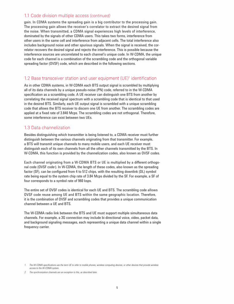
gain . In CDMA systems the spreading gain is a big contributor to the processing gain . The processing gain allows the receiver’s correlator to extract the desired signal from the noise . When transmitted, a CDMA signal experiences high levels of interference, dominated by the signals of other CDMA users . This takes two forms, interference from other users in the same cell and interference from adjacent cells . The total interference also includes background noise and other spurious signals . When the signal is received, the cor-relator recovers the desired signal and rejects the interference . This is possible because the interference sources are uncorrelated to each channel’s unique code . In W-CDMA, the unique code for each channel is a combination of the scrambling code and the orthogonal variable spreading factor (OVSF) code, which are described in the following sections .
1.2 Base transceiver station and user equipment (UE)1 identificationAs in other CDMA systems, in W-CDMA each BTS output signal is scrambled by multiplying all of its data channels by a unique pseudo-noise (PN) code, referred to in the W-CDMA specification as a scrambling code . A UE receiver can distinguish one BTS from another by correlating the received signal spectrum with a scrambling code that is identical to that used in the desired BTS . Similarly, each UE output signal is scrambled with a unique scrambling code that allows the BTS receiver to discern one UE from another . The scrambling codes are applied at a fixed rate of 3 .840 Mcps . The scrambling codes are not orthogonal . Therefore, some interference can exist between two UEs .
1.3 Data channelization Besides distinguishing which transmitter is being listened to, a CDMA receiver must further distinguish between the various channels originating from that transmitter . For example, a BTS will transmit unique channels to many mobile users, and each UE receiver must distinguish each of its own channels from all the other channels transmitted by the BTS . In W-CDMA, this function is provided by the channelization codes, also known as OVSF codes .
Each channel originating from a W-CDMA BTS or UE is multiplied by a different orthogo-nal code (OVSF code2) . In W-CDMA, the length of these codes, also known as the spreading factor (SF), can be configured from 4 to 512 chips, with the resulting downlink (DL) symbol rate being equal to the system chip rate of 3 .84 Mcps divided by the SF . For example, a SF of four corresponds to a symbol rate of 960 ksps .
The entire set of OVSF codes is identical for each UE and BTS . The scrambling code allows OVSF code reuse among UE and BTS within the same geographic location . Therefore, it is the combination of OVSF and scrambling codes that provides a unique communication channel between a UE and BTS .
The W-CDMA radio link between the BTS and UE must support multiple simultaneous data channels . For example, a 3G connection may include bi-directional voice, video, packet data, and background signaling messages, each representing a unique data channel within a single frequency carrier .
1. The W-CDMA specifications use the term UE to refer to mobile phones, wireless computing devices, or other devices that provide wireless access to the W-CDMA system.
2. The synchronization channels are an exception to this, as described later.
1.1 Code division multiple access (continued)
5
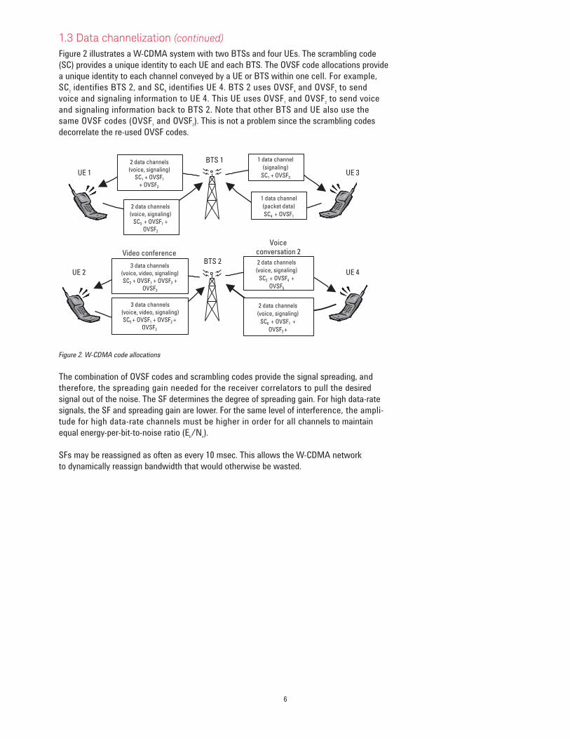
Figure 2 illustrates a W-CDMA system with two BTSs and four UEs . The scrambling code (SC) provides a unique identity to each UE and each BTS . The OVSF code allocations provide a unique identity to each channel conveyed by a UE or BTS within one cell . For example, SC2 identifies BTS 2, and SC6 identifies UE 4 . BTS 2 uses OVSF4 and OVSF5 to send voice and signaling information to UE 4 . This UE uses OVSF1 and OVSF2 to send voice and signaling information back to BTS 2 . Note that other BTS and UE also use the same OVSF codes (OVSF1 and OVSF2) . This is not a problem since the scrambling codes decorrelate the re-used OVSF codes . Figure 2. W-CDMA code allocations
The combination of OVSF codes and scrambling codes provide the signal spreading, and therefore, the spreading gain needed for the receiver correlators to pull the desired signal out of the noise . The SF determines the degree of spreading gain . For high data-rate signals, the SF and spreading gain are lower . For the same level of interference, the ampli-tude for high data-rate channels must be higher in order for all channels to maintain equal energy-per-bit-to-noise ratio (Eb/No) .
SFs may be reassigned as often as every 10 msec . This allows the W-CDMA network to dynamically reassign bandwidth that would otherwise be wasted .
2 data channels(voice, signaling)
SC3 + OVSF1 +OVSF2
1 data channel(packet data)SC4 + OVSF1
2 data channels(voice, signaling)
SC1 + OVSF1
+ OVSF2
1 data channel(signaling)
SC1 + OVSF3
Video conference
3 data channels(voice, video, signaling)SC2 + OVSF1 + OVSF2 +
OVSF3
3 data channels(voice, video, signaling)SC5 + OVSF1 + OVSF2 +
OVSF3
2 data channels(voice, signaling)
SC2 + OVSF4 +OVSF5
2 data channels(voice, signaling)
SC6 + OVSF1 +OVSF2 +
Voiceconversation 2
BTS 1
BTS 2
UE 1
UE 2
UE 3
UE 4
1.3 Data channelization (continued)
6

1.4 Slots, frames, and power controlsAll W-CDMA uplink (UL) and DL data channels are segmented into time slots and frames . A slot is 666 .667 µsec in length, equal in duration to 2560 chips of the system chip rate . Fifteen of these time slots are concatenated to form a 10 ms frame (Figure 3) . The frame is the fundamental unit of time associated with channel coding and interleaving processes . However, certain time-critical information, such as power control bits, are transmitted in every time slot . This facilitates UE power control updates at a rate of 1500 adjustments per second to optimize cell capacity .
Figure 3. W-CDMA slot and frame structure
In any cellular CDMA system, the BTS must precisely control the transmit power of the UEs at a rate sufficient to optimize the link budget . This is referred to as UL power control . The goal is to balance the power received at the BTS from all UEs within a few dB, which is essential to optimizing the UL spread spectrum link budget . The UE also sends power con-trol bits to the BTS at the same rate, and the BTS responds by adjusting the power of the data channels that are intended for the respective UE . This is referred to as DL power control .
1.5 Protocol structureThe protocol structure of the W-CDMA system closely follows the industry standard Open System Interconnection (OSI) model . Figure 4 shows the three bottom layers .
Figure 4. W-CDMA protocol structure
The network layer (layer 3) is based heavily on GSM standards . It is responsible for connecting services from the network to UE . The data link layer (layer 2) is composed of two main functional blocks: the radio link control (RLC) and medium access control (MAC) blocks . The RLC block is responsible for the transfer of user data, error correction, flow control, protocol error detection and recovery, and ciphering . The MAC function at layer 2 is responsible for mapping between logical channels and transport channels (see following section) as well as providing the multiplexing/de-multiplexing function of various logical channels efficiently onto the same transport channel . The physical layer (layer 1) maps the transport channels on to the physical channels and performs all of the RF functions necessary to make the system work . These functions
0 1 2 3 4 5 6 7 8 9 10 11 12 13 14
W-CDMA frame (10 ms)
Network layerlayer 3
Data link layerlayer 2
Physical layerlayer 1
Transport channels
Physical channels
Logical channels
Radio link control (RLC)
Medium access control (MAC)
Radio resource control (RRC)
7

include operations such as frequency and time synchronization, rate matching, spreading and modulation, power control, and soft handoff . This application note focuses on layer 1 and refers to layer 2 briefly when appropriate . For more information on layer 2 and above, refer to the 3GPP specifications documents available on their web site (www.3gpp.org/specifications) .
1.6 Logical, transport, and physical channelsLogical channels are the information content, which will ultimately be transmitted over the physical channels . Logical channels include the Broadcast Control Channel (BCCH), the Paging Control Channel (PCCH), the Common Control Channel (CCCH), and Dedicated Control and Traffic Channels (DCCH, DTCH) .
W-CDMA introduces the concept of transport channels to support sharing physical resources between multiple services . Each service, such as data, fax, voice, or signaling is routed into different transport channels by the upper signaling layers . These services may have different data-rates and error control mechanisms . The transport channels are then multiplexed as required prior to transmission via one or more physical channels . High data-rate services or a combination of lower-rate transport channels may be multiplexed into several physical channels . This flexibility allows numerous transport channels (services) of varying data rates to be efficiently allocated to physical channels . By multiplexing these transport channels efficiently, system capacity is optimized . For example, if the aggregate data rate of three transport channels exceeds the maximum of a single physical channel, then the data can be routed to two lower rate physical channels that closely match the total required data rate . Transport channels include the Broadcast Channel (BCH), the Paging Channel (PCH), the Forward Access Channel (FACH), the Dedicated Channel (DCH) and the Random Access Channel (RACH) .
The W-CDMA DL is composed of a number of physical channels . The most important DL physical channels are the Common Pilot Channel (CPICH), the Primary Common Control Physical Channel (P-CCPCH), the Secondary Common Control Physical Channel (S-CCPCH), and the Dedicated Physical Data and Control Channels (DPDCH/DPCCH) . The UL consists of a Physical Random Access Channel (PRACH), a Physical Common Packet Channel (PCPCH), and Dedicated Physical Data and Control Channels (DPDCH/DPCCH) . These channels are described in the following sections .
Figure 5 shows an example of channel mapping for the DL . When a UE is in the idle mode, the BTS sends dedicated signaling information from the DCCH logical channel through the FACH transport channel . This maps the information onto the S-CCPCH physical channel for transmission to a UE . When the UE is in the dedicated connection mode, the same signaling information is routed through the DCH transport channel . This maps the information onto the DPDCH/DPCCH physical channel for trans-mission to the UE .
1.5 Protocol structure (continued)
8
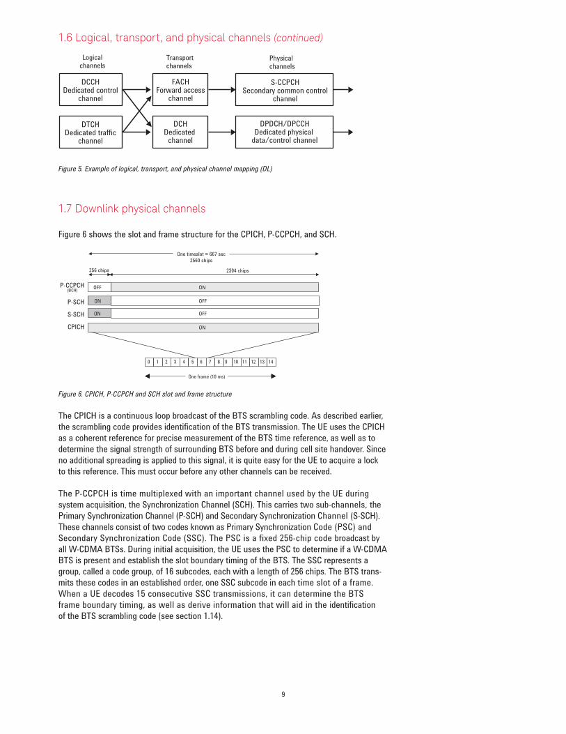
Figure 5. Example of logical, transport, and physical channel mapping (DL)
1.7 Downlink physical channels Figure 6 shows the slot and frame structure for the CPICH, P-CCPCH, and SCH .
Figure 6. CPICH, P-CCPCH and SCH slot and frame structure
The CPICH is a continuous loop broadcast of the BTS scrambling code . As described earlier, the scrambling code provides identification of the BTS transmission . The UE uses the CPICH as a coherent reference for precise measurement of the BTS time reference, as well as to determine the signal strength of surrounding BTS before and during cell site handover . Since no additional spreading is applied to this signal, it is quite easy for the UE to acquire a lock to this reference . This must occur before any other channels can be received .
The P-CCPCH is time multiplexed with an important channel used by the UE during system acquisition, the Synchronization Channel (SCH) . This carries two sub-channels, the Primary Synchronization Channel (P-SCH) and Secondary Synchronization Channel (S-SCH) . These channels consist of two codes known as Primary Synchronization Code (PSC) and Secondary Synchronization Code (SSC) . The PSC is a fixed 256-chip code broadcast by all W-CDMA BTSs . During initial acquisition, the UE uses the PSC to determine if a W-CDMA BTS is present and establish the slot boundary timing of the BTS . The SSC represents a group, called a code group, of 16 subcodes, each with a length of 256 chips . The BTS trans-mits these codes in an established order, one SSC subcode in each time slot of a frame . When a UE decodes 15 consecutive SSC transmissions, it can determine the BTS frame boundary timing, as well as derive information that will aid in the identification of the BTS scrambling code (see section 1 .14) .
DCCHDedicated control
channel
DTCHDedicated traffic
channel
FACHForward access
channel
DCHDedicated
channel
S-CCPCHSecondary common control
channel
DPDCH/DPCCHDedicated physical
data/control channel
Logicalchannels
Transportchannels
Physicalchannels
0 1 2 3 4 5 6 7 8 9 10 11 12 13 14
P-CCPCH(BCH)
P-SCH
S-SCH
CPICH
ON OFF
One timeslot = 667 sec2560 chips
ON OFF
OFF ON
ON
256 chips 2304 chips
One frame (10 ms)
1.6 Logical, transport, and physical channels (continued)
9
The SCH is transmitted during the first 256 chips of each time slot while the P-CCPCH is off (Figure 6) . During the remaining 2304 chips of each slot the P-CCPCH, which contains 18 bits of broadcast data (Broadcast Channel (BCH) information) at a rate of 15 kbps, is transmitted . Since the cell’s broadcast parameters message will require more than 18 bits, the broadcast information may span several frames .
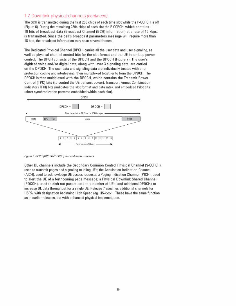
The Dedicated Physical Channel (DPCH) carries all the user data and user signaling, as well as physical channel control bits for the slot format and the UE inner loop power control . The DPCH consists of the DPDCH and the DPCCH (Figure 7) . The user’s digitized voice and/or digital data, along with layer 3 signaling data, are carried on the DPDCH . The user data and signaling data are individually treated with error protection coding and interleaving, then multiplexed together to form the DPDCH . The DPDCH is then multiplexed with the DPCCH, which contains the Transmit Power Control (TPC) bits (to control the UE transmit power), Transport Format Combination Indicator (TFCI) bits (indicates the slot format and data rate), and embedded Pilot bits (short synchronization patterns embedded within each slot) .
Figure 7. DPCH (DPDCH/DPCCH) slot and frame structure
Other DL channels include the Secondary Common Control Physical Channel (S-CCPCH), used to transmit pages and signaling to idling UEs; the Acquisition Indication Channel (AICH), used to acknowledge UE access requests; a Paging Indication Channel (PICH), used to alert the UE of a forthcoming page message; a Physical Downlink Shared Channel (PDSCH), used to dish out packet data to a number of UEs; and additional DPDCHs to increase DL data throughput for a single UE . Release 7 specifies additional channels for HSPA, with designation beginning High Speed (eg . HS-xxxx) . These have the same function as in earlier releases, but with enhanced physical implemetation .
1 2 3 4 5 6 7 8 9 10 11 12 13 14
One frame (10 ms)
DPCCH = DPDCH =
One timeslot = 667 sec = 2560 chips
Data Data TPC PilotTFCI
DPCH
0
1.7 Downlink physical channels (continued)
10
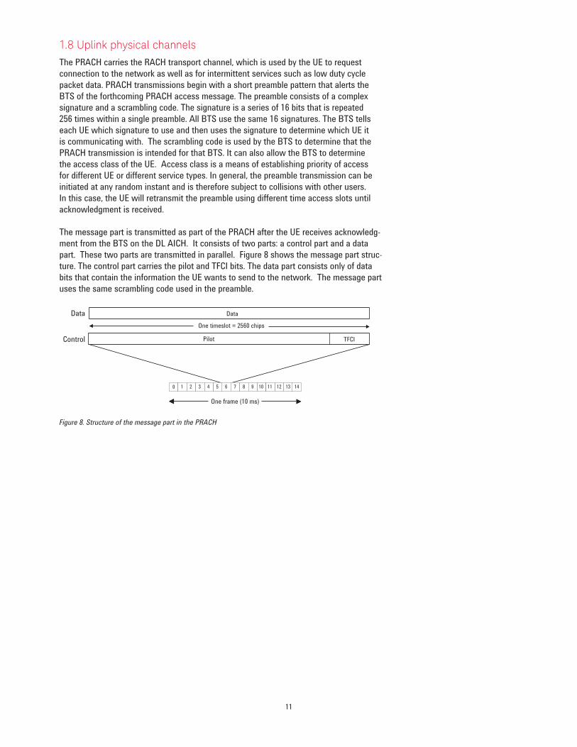
1.8 Uplink physical channelsThe PRACH carries the RACH transport channel, which is used by the UE to request connection to the network as well as for intermittent services such as low duty cycle packet data . PRACH transmissions begin with a short preamble pattern that alerts the BTS of the forthcoming PRACH access message . The preamble consists of a complex signature and a scrambling code . The signature is a series of 16 bits that is repeated 256 times within a single preamble . All BTS use the same 16 signatures . The BTS tells each UE which signature to use and then uses the signature to determine which UE it is communicating with . The scrambling code is used by the BTS to determine that the PRACH transmission is intended for that BTS . It can also allow the BTS to determine the access class of the UE . Access class is a means of establishing priority of access for different UE or different service types . In general, the preamble transmission can be initiated at any random instant and is therefore subject to collisions with other users . In this case, the UE will retransmit the preamble using different time access slots until acknowledgment is received .
The message part is transmitted as part of the PRACH after the UE receives acknowledg-ment from the BTS on the DL AICH . It consists of two parts: a control part and a data part . These two parts are transmitted in parallel . Figure 8 shows the message part struc-ture . The control part carries the pilot and TFCI bits . The data part consists only of data bits that contain the information the UE wants to send to the network . The message part uses the same scrambling code used in the preamble .
Figure 8. Structure of the message part in the PRACH
1 2 3 4 5 6 7 8 9 10 11 12 13 14
One frame (10 ms)
One timeslot = 2560 chips
Pilot TFCI
0
Data
Control
Data
11
Subframe #0 Subframe #i Subframe #4
HARQ-ACK C Q I/PCI
One radio frame Tf = 10 ms
One HS-DPCCH subframe (2 ms)
2 Tslot = 5120 chipsTslot = 2560 chips X
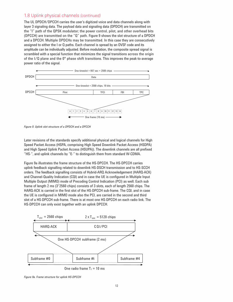
The UL DPDCH/DPCCH carries the user’s digitized voice and data channels along with layer 3 signaling data . The payload data and signaling data (DPDCH) are transmitted on the “I” path of the QPSK modulator; the power control, pilot, and other overhead bits (DPCCH) are transmitted on the “Q” path . Figure 9 shows the slot structure of a DPDCH and a DPCCH . Multiple DPDCHs may be transmitted . In this case they are consecutively assigned to either the I or Q paths . Each channel is spread by an OVSF code and its amplitude can be individually adjusted . Before modulation, the composite spread signal is scrambled with a special function that minimizes the signal transitions across the origin of the I/Q plane and the 0° phase shift transitions . This improves the peak-to-average power ratio of the signal .
Figure 9. Uplink slot structure of a DPDCH and a DPCCH
Later revisions of the standards specify additional physical and logical channels for High Speed Packet Access (HSPA, comprising High Speed Downlink Packet Access (HSDPA) and High Speed Uplink Packet Access (HSUPA)) . The downlink channels are all prefixed “HS-“, and uplink channels by “E-“ to distinguish them from standard W-CDMA .
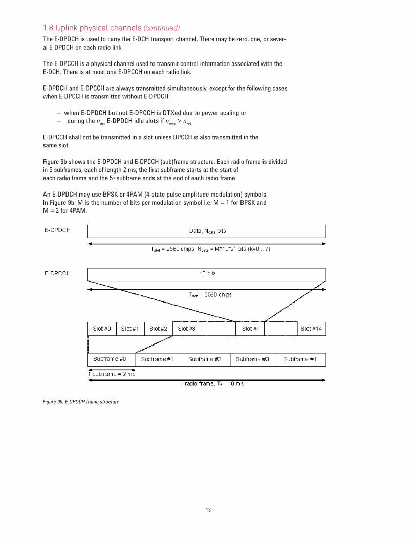
Figure 9a illustrates the frame structure of the HS-DPCCH . The HS-DPCCH carries uplink feedback signalling related to downlink HS-DSCH transmission and to HS-SCCH orders . The feedback signalling consists of Hybrid-ARQ Acknowledgement (HARQ-ACK) and Channel-Quality Indication (CQI) and in case the UE is configured in Multiple Input Multiple Output (MIMO) mode of Precoding Control Indication (PCI) as well . Each sub frame of length 2 ms (3*2560 chips) consists of 3 slots, each of length 2560 chips . The HARQ-ACK is carried in the first slot of the HS-DPCCH sub-frame . The CQI, and in case the UE is configured in MIMO mode also the PCI, are carried in the second and third slot of a HS-DPCCH sub-frame . There is at most one HS-DPCCH on each radio link . The HS-DPCCH can only exist together with an uplink DPCCH .
Figure 9a. Frame structure for uplink HS-DPCCH
1 2 3 4 5 6 7 8 9 10 11 12 13 14
One frame (10 ms)
One timeslot = 667 sec = 2560 chips
Pilot TFCI
0
DPDCH
DPCCH
Data
One timeslot = 2560 chips, 10 bits
FBI TPC
1.8 Uplink physical channels (continued)
12
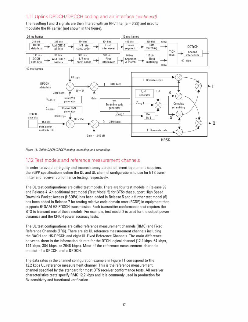
The E-DPDCH is used to carry the E-DCH transport channel . There may be zero, one, or sever-al E-DPDCH on each radio link .
The E-DPCCH is a physical channel used to transmit control information associated with the E-DCH . There is at most one E-DPCCH on each radio link .
E-DPDCH and E-DPCCH are always transmitted simultaneously, except for the following cases when E-DPCCH is transmitted without E-DPDCH:
– when E-DPDCH but not E-DPCCH is DTXed due to power scaling or – during the ndtx E-DPDCH idle slots if nmax > ntx1
E-DPCCH shall not be transmitted in a slot unless DPCCH is also transmitted in the same slot .
Figure 9b shows the E-DPDCH and E-DPCCH (sub)frame structure . Each radio frame is divided in 5 subframes, each of length 2 ms; the first subframe starts at the start of each radio frame and the 5th subframe ends at the end of each radio frame .
An E-DPDCH may use BPSK or 4PAM (4-state pulse amplitude modulation) symbols . In Figure 9b, M is the number of bits per modulation symbol i .e . M = 1 for BPSK and M = 2 for 4PAM .
Figure 9b. E-DPDCH frame structure
1.8 Uplink physical channels (continued)
13

1.9 Transport format detectionThe number of possible arrangements of the W-CDMA air interface numbers in the millions . For any given connection only a small subset of these are needed . To make operation practical, that subset, known as the Transport Format Combination Set (TFCS), is communicated from the network to the UE at the time of connection setup . The TFCS includes all of the allowable Transport Formats (TF) and the associated data capacity for each of the channels that can be present in the link, and all of the allowable Transport Format Combinations (TFC) for the link . The Network’s Radio Resource Control (RRC) entity provides this information to its lower layers . The UE’s RRC entity does the same for its lower layers upon receiving the TFCS from the network .
Once this information is shared between the two, the transmitter can use it, along with the demands for transmission capacity from higher layers, to decide which channels shall be present and how each channel will be arranged in the radio frame . Likewise the receiver can use it to determine which channels are present and how to recover each channel that is present .
The W-CDMA system provides two methods to make this determination . The first of these is the inclusion of a Transport Format Combination Indicator (TFCI) in each radio frame . The second is Blind Transport Format Detection (BTFD) .
When TFCI is used, the transmitting side determines which Transport Format Combination it will use . It then includes the TFCI, which is an index to the list of allowable combina-tions in the TFCS, in the control portion of the DPCH . The receiver always knows how to recover the TFCI, which it then uses to determine which channels to try to recover and how to decode each one .
When BTFD is used, the receiver must try every allowable TFC in the TFCS to determine which one results in the least errors .
14

1.10 Downlink DPDCH/DPCCH coding and air interfaceFigure 10 shows an example of the coding, spreading, and scrambling for the DPCH . In this example, a 12 .2 kbps voice service is carried on a DTCH logical channel that uses 20 ms frames . After channel coding, the DTCH is coded with a 1/3 rate convolutional encoder . In this example, the data is then punctured (rate matching) and interleaved . At this point, the DTCH is segmented into 10 ms frames to match the physical channel frame rate . The DCCH logical channel carries a 2 .5 kbps data stream on a 40 ms frame structure . The DCCH is coded in the same manner as the DTCH . Frame segmentation for the DCCH involves splitting the data into four 10 ms segments to match the physical channel frame rate . The DTCH and DCCH are multiplexed together to form the Coded Composite Transport Channel (CCTrCH) . The CCTrCH is interleaved and mapped onto a DPDCH running at 42 kbps .
In this example, the DPCCH is running at a rate of 18 kbps . The DPDCH and DPCCH are time muliplexed together to form a 60 kbps stream (DPCH) . This stream is converted into separate I and Q channels with a symbol rate of 30 ksps for each channel . The DPCH is spread with an OVSF code with spread factor equal to 128 (to reach the desired 3 .84 Mcps), which differentiates the signal from others within the cell or sector . After that process, it is complex scrambled with a code that identifies each cell or sector . The resulting I and Q signals are then filtered and used to modulate the RF carrier (not shown in the figure) .
Figure 10. Downlink DPDCH/DPCCH coding, spreading, and scrambling.
S - POVSFcode
generator
I
Q
Complexscramble code
generator
Q
I+
+
+
-
Spreading
Q scramble
I scramble
I scramble
DPCCH
Time multiplexer
CCTrCH
Complexscrambling
Add CRC &tail bits
DTCHdata bits
Add CRC &tail bits
DCCHdata bits Conv. coder
Conv. coder Ratematching
Ratematching
Interleaver
Interleaver
Framesegment
Framesegment
TrCHmux Interleaver
15

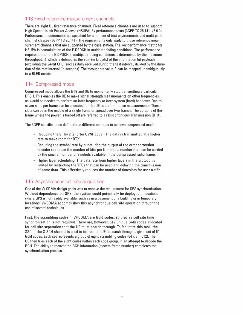
1.11 Uplink DPDCH/DPCCH coding and air interfaceThe spreading and scrambling used on the UL DPDCH/DPCCH differs from the DL in two key areas: I/Q multiplexing and hybrid phase shift keying (HPSK) scrambling instead of complex scrambling) . Figure 11 shows an example of the coding and air interface for a DPCCH interface for a UL DPDCH and a DPCCH . In this example, the logical DTCH carries a 12 .2 kbps voice channel and the logical DCCH carries a 2 .5 kbps signaling channel . Each of these logical channels is channel coded, convolutionally coded, and interleaved . The DTCH uses 20 ms frames . At the frame segmentation point, the DTCH is split into two parts to conform with the physical layer’s 10 ms frame structure . The DCCH, which operates with 40 ms frames, is split into four parts so that each signaling frame is spread over four 10 ms radio frames . These channels are then punctured (rate matching) and multiplexed prior to spreading . The multiplexed data at this point is called the Coded Composite Transport Channel (CCTrCH) . After a second interleaving, the CCTrCH is mapped onto a DPDCH running at 60 kbps . The DPDCH is spread with an OVSF code with spread factor equal to 64 in order to reach the desired 3 .84 Mcps . After gain scaling (to adjust the transmission power for the variable spreading factor), the spread DPDCH is applied to the I channel .
The data rate for the UL DPCCH is always 15 kbps . The DPCCH data is spread with an OVSF code with SF = 256 to reach the 3 .84 Mcps rate and is gain scaled in this example to be –6 dB relative to the DPDCH . The DPCCH is then applied to the Q channel .
If additional DPDCHs were present they would be assigned to I or Q and spread with the appropriate OVSF code . Before modulation, the composite spread signal is scrambled with a special complex function that limits the signal transitions across the origin of the I/Q plane and the 0° phase shift transitions . This improves its peak-to-aver-age power ratio . This function can be considered a variation of regular complex scram-bling and is commonly known as HPSK, although this term is not mentioned in the 3GPP specifications . The scrambling generator produces two random sequences (referenced in the 3GPP specifications as Clong,1 and Clong,2, if long scrambling sequences are used) .
The second sequence is decimated, multiplied by the function {1,-1} and by the first sequence, and applied to the Q path of the complex scrambler . The first sequence is applied to the I path of the complex scrambler .
16
The resulting I and Q signals are then filtered with an RRC filter (a = 0 .22) and used to modulate the RF carrier (not shown in the figure) .
Figure 11. Uplink DPCH/DPCCH coding, spreading, and scrambling.
1.12 Test models and reference measurement channelsIn order to avoid ambiguity and inconsistency across different equipment suppliers, the 3GPP specifications define the DL and UL channel configurations to use for BTS trans-mitter and receiver conformance testing, respectively .
The DL test configurations are called test models . There are four test models in Release 99 and Release 4 . An additional test model (Test Model 5) for BTSs that support High Speed Downlink Packet Access (HSDPA) has been added in Release 5 and a further test model (6) has been added in Release 7 for testing relative code domain error (RCDE) in equipment that supports 64QAM HS-PDSCH transmission . Each transmitter conformance test requires the BTS to transmit one of these models . For example, test model 2 is used for the output power dynamics and the CPICH power accuracy tests .
The UL test configurations are called reference measurement channels (RMC) and Fixed Reference Channels (FRC) . There are six UL reference measurement channels including the RACH and HS-DPCCH and eight UL Fixed Reference Channels . The main difference between them is the information bit rate for the DTCH logical channel (12 .2 kbps, 64 kbps, 144 kbps, 384 kbps, or 2048 kbps) . Most of the reference measurement channels consist of a DPCCH and a DPDCH .
The data rates in the channel configuration example in Figure 11 correspond to the 12 .2 kbps UL reference measurement channel . This is the reference measurement channel specified by the standard for most BTS receiver conformance tests . All receiver characteristics tests specify RMC 12 .2 kbps and it is commonly used in production for Rx sensitivity and functional verification .
Add CRC &tail bits
268 bits
Pilot, powercontrol & TFCI
15 kbps
3840 kcpsSF = 256
Data OVSFgenerator
3840 kcpsSF = 64
244 bits 804 bitsFirst
interleaver
804 bitsRate
matching
490 bits
Gain = –2.69 dB
Gain
Complexscrambling
I+
+
+
–1, –1
I 3840 kcps
Q 3840 kcps
402 bitsFrame
segment
60 kbps
Control OVSFgenerator
Cch,256,0
Cch,64,16
I Scramble code
I Scramble code
Q
Q
DTCHdata bits
120 bits100 bits 360 bits 360 bits 110 bits90 bits
DPDCHdata bits
40 ms frames
10 ms frames49 kbps
Add CRC &tail bits
1/3 rateconv. coder
11 kbps
Segment& match
DCCHdata bits
TrCHmux
60 kbps
CCTrCHSecond
interleaver
Clong,1
Clong,2
HPSK
20 ms frames
Q
1/3 rateconv. coder
Ratematching
Firstinterleaver
1, –1Generator
Deciby 2
225 Scramble code
generator
DPCCHdata bits
1.11 Uplink DPDCH/DPCCH coding and air interface (continued)
17
1.13 Fixed reference measurement channelsThere are eight UL fixed reference channels . Fixed reference channels are used to support High Speed Uplink Packet Access (HSUPA) Rx performance tests (3GPP TS 25 .141 v8 .6 .0) . Performance requirements are specified for a number of test environments and multi-path channel classes (3GPP TS 25 .141) . The requirements only apply to those reference mea-surement channels that are supported by the base station . The key performance metric for HSUPA is demodulation of the E-DPDCH in multipath fading conditions . The performance requirement of the E-DPDCH in multipath fading conditions is determined by the minimum throughput, R, which is defined as the sum (in kilobits) of the information bit payloads (excluding the 24-bit CRC) successfully received during the test interval, divided by the dura-tion of the test interval (in seconds) . The throughput value R can be mapped unambiguously to a BLER metric .
1.14 Compressed modeCompressed mode allows the BTS and UE to momentarily stop transmitting a particular DPCH . This enables the UE to make signal strength measurements on other frequencies, as would be needed to perform an inter-frequency or inter-system (hard) handover . One to seven slots per frame can be allocated for the UE to perform these measurements . These slots can be in the middle of a single frame or spread over two frames . The portions of the frame where the power is turned off are referred to as Discontinuous Transmission (DTX) .
The 3GPP specifications define three different methods to achieve compressed mode:
– Reducing the SF by 2 (shorter OVSF code) . The data is transmitted at a higher rate to make room for DTX .
– Reducing the symbol rate by puncturing the output of the error correction encoder to reduce the number of bits per frame to a number that can be carried by the smaller number of symbols available in the compressed radio frame .
– Higher layer scheduling . The data rate from higher layers in the protocol is limited by restricting the TFCs that can be used and delaying the transmission of some data . This effectively reduces the number of timeslots for user traffic .
1.15 Asynchronous cell site acquisitionOne of the W-CDMA design goals was to remove the requirement for GPS synchronization . Without dependence on GPS, the system could potentially be deployed in locations where GPS is not readily available, such as in a basement of a building or in temporary locations . W-CDMA accomplishes this asynchronous cell site operation through the use of several techniques .
First, the scrambling codes in W-CDMA are Gold codes, so precise cell site time synchronization is not required . There are, however, 512 unique Gold codes allocated for cell site separation that the UE must search through . To facilitate this task, the SSC in the S-SCH channel is used to instruct the UE to search through a given set of 64 Gold codes . Each set represents a group of eight scrambling codes (64 x 8 = 512) . The UE then tries each of the eight codes within each code group, in an attempt to decode the BCH . The ability to recover the BCH information (system frame number) completes the synchronization process .
18

1.16 Asynchronous cell site soft handoverIn W-CDMA soft handover, a UE can establish simultaneous communication with several BTSs . During soft handover the combined signals from each BTS are individually correlated and then combined . As such, communication is possible in situations where an individual signal from a single BTS might otherwise be too weak to support the radio link .
Because each W-CDMA BTS operates on an asynchronous clock, soft handover is complicated by the fact that frame timing between BTSs is not explicitly coordinated . The UE could therefore have a difficult time combining frames from different BTSs . To get around this problem, the W-CDMA UE measures the frame timing differential between the originating BTS and the handover target BTS . The UE reports this frame timing back to the network, which then issues a frame timing adjustment command to the target BTS . The target BTS adjusts the frame timing of the DPDCH/DPCCH channel that is being transmitted so the UE receives the target BTS frames in close time alignment with the corresponding frames from the originating BTS . With this time alignment feature, UE’s rake receiver is able to track the received signals from both BTSs .
19
2. General Design and Measurement Issues
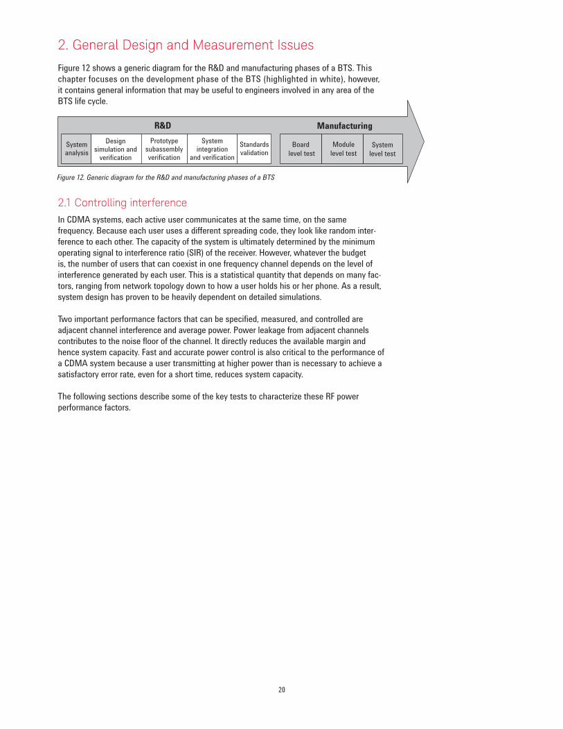
Figure 12 shows a generic diagram for the R&D and manufacturing phases of a BTS . This chapter focuses on the development phase of the BTS (highlighted in white), however, it contains general information that may be useful to engineers involved in any area of the BTS life cycle .
2.1 Controlling interferenceIn CDMA systems, each active user communicates at the same time, on the same frequency . Because each user uses a different spreading code, they look like random inter-ference to each other . The capacity of the system is ultimately determined by the minimum operating signal to interference ratio (SIR) of the receiver . However, whatever the budget is, the number of users that can coexist in one frequency channel depends on the level of interference generated by each user . This is a statistical quantity that depends on many fac-tors, ranging from network topology down to how a user holds his or her phone . As a result, system design has proven to be heavily dependent on detailed simulations .
Two important performance factors that can be specified, measured, and controlled are adjacent channel interference and average power . Power leakage from adjacent channels contributes to the noise floor of the channel . It directly reduces the available margin and hence system capacity . Fast and accurate power control is also critical to the performance of a CDMA system because a user transmitting at higher power than is necessary to achieve a satisfactory error rate, even for a short time, reduces system capacity .
The following sections describe some of the key tests to characterize these RF power performance factors .
Systemanalysis
Modulelevel test
Systemlevel test
R&D Manufacturing
Board level test
Designsimulation and
verification
Systemintegration
and verification
Standardsvalidation
Prototypesubassemblyverification
Figure 12. Generic diagram for the R&D and manufacturing phases of a BTS
20

2.1.1 Average RF power Average RF power will probably remain the preferred measurement for manufacturing testing, even for sophisticated modulation schemes such as CDMA; but for any modulated signal, average RF power is only part of the picture . In the research and development phase, engineers are interested in peak power, peak to average power ratio (PAR), and, particularly for CDMA, power statistics such as the complementary cumulative distribution function (CCDF) — described later in the chapter .
The preferred solution is to measure average power using a signal analyzer with a channel power measurement . Care must be taken to ensure that the amplitude accuracy of the instrument meets the needs of the measurement specifications . For some analyzers, the absolute amplitude accuracy is as low as 0 .6 dB (similar to a power meter’s accuracy .) For others, the accuracy can be more than ±1 dB, though the relative accuracy is usually much better than ±1 dB . An advantage of using a signal analyzer is that it provides a larger suite of required measurements, including modulation quality analysis . The specifications for 6 .2 .1 BTS maximum output power in define the output power as the mean power level per carrier measured at the antenna connector .
21
2.1.2 Adjacent channel interference Depending on the context, the acronym ACP(R) has been taken to mean either adjacent channel power (ratio), which is a transmitter measurement, or adjacent channel protection (ratio), which is a receiver measurement . To resolve this ambiguity, 3GPP has introduced three new terms: adjacent channel leakage power ratio (ACLR), adjacent channel selectivity (ACS), and adjacent channel interference ratio (ACIR) .
ACLR is a measure of transmitter performance . It is defined as the ratio of the transmitted power to the power measured after a receiver filter in the adjacent RF channel . This is what was formerly called adjacent channel power ratio .
ACS is a measure of receiver performance . It is defined as the ratio of the receiver filter attenuation on the assigned channel frequency to the receiver filter attenuation on the adjacent channel frequency .
ACIR is a measure of overall system performance . It is defined as the ratio of the total power transmitted from a source (BTS or UE) to the total interference power resulting from both transmitter and receiver imperfections affecting a victim receiver . ACIR is mainly of interest in network simulation where the total amount of interference, rather than the source of the interference, is the primary concern . This is what was formerly called adjacent channel protection ratio .
The following equation shows the relationship between ACIR, ACLR, and ACS:
The main source of adjacent channel leakage (ACL) is non-linear effects in the power amplifiers (PA) . ACL directly affects the co-existing performance of systems on adjacent channels . Power leakage is a general noise pollution and degrades performance of the system in the adjacent channel . If sufficiently bad, it can cause the so called “near-far” problem, where a BTS simply cannot communicate with a far away UE because of high ACL from a nearby adjacent channel BTS . Network planning can address this problem, but the associated costs depend directly on the stringency of the ACLR specification . So, we have conflicting needs . From an equipment design perspective a relaxed ACLR specification is attractive, whereas from a network planning perspective, low ACL is very desirable .
There has been much discussion of this within the specifications committees . The current values in the 3GPP specifications for the BTS are 45 dB at 5 MHz offset and 50 dB at 10 MHz offset .
ACIR = 1
1ACLR
1ACS+
22
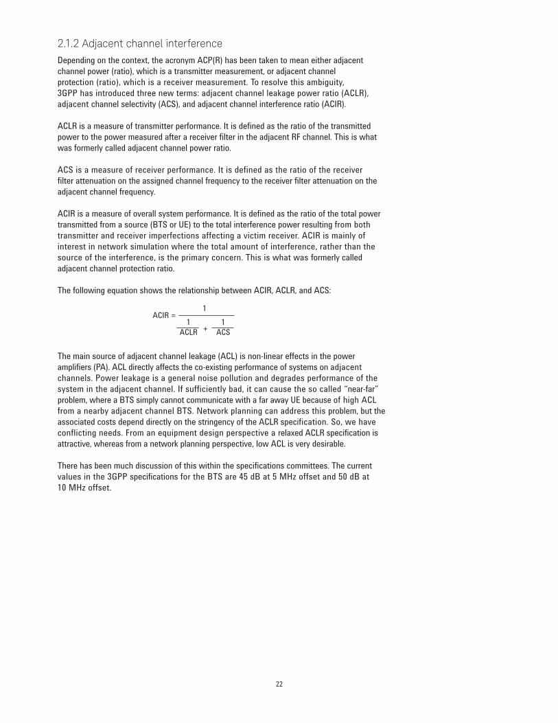
ACLR (or ACPR) is commonly measured using a signal analyzer or measuring receiver . In the measurement, filtering is applied to both the power in the main frequency channel and the power in the adjacent channel . An important factor for ACLR is the specification of the measurement filter, including its bandwidth and shape . Original W-CDMA specifications called for a rectangular filter, but this has now changed to a RRC filter with a –3 dB bandwidth equal to the chip rate . This provides a closer indication to real-life performance . However, it requires the measuring instrument to apply precise filter weighting . This may preclude making the measurement with existing spectrum analyzers that do not have partic-ular W-CDMA ACLR capability, although in reality, the difference in the measurement result is very small (around 0 .1 dB) . Figure 13 shows an ACLR measurement for a W-CDMA DL signal configured as test model 1 with 16 DPCHs . The measurement was performed using a vector signal analyzer with the appropriate RRC filter, as specified .
Figure 13. ACLR measurement for test model 1 with 16 DPCHs.
2.2 Handling high peak-to-average power ratios (PAR)ACLR is a key parameter, but why is it a particular challenge to maintain good ACLR performance for a W-CDMA BTS?
Some of the 2G systems, such as GSM, use a constant modulation format (Gaussian minimum shift keying (GMSK)) . GSM has the advantage of having a constant amplitude envelope, which allows the use of less expensive, non-linear, class B PAs .
By contrast, CDMA systems use non-constant modulation formats . PAR is the ratio of the peak envelope power to the average envelope power of a signal . In general, low PARs are desirable, which reduce the required PA linear dynamic range .
2.1.2 Adjacent channel interference (continued)
23

In CDMA systems, multiple channels are added to modulate a single carrier . The PAR increases as code channels are activated . A PAR of 8 dB is not uncommon for a W-CDMA DL multi-channel signal . Amplifier design for W-CDMA BTS is particularly challenging because the amplifier must be capable of handling the high PAR the signal exhibits, while main-taining a good ACL performance . The use of multi-carrier power amplifiers pushes design complexity one step further .
Both the amplifier designer and the system integrator must make sure the PA (and other components) can handle the PAR for stressful channel configurations, while maintaining a good ACL performance . You can use the complementary cumulative distribution function (CCDF) to help you with this task .
2.2.1 Complementary cumulative distribution functionThe CCDF fully characterizes the power statistics of a signal . It provides PAR versus probability . Figure 14 shows the CCDF curves for two W-CDMA DL signals with different channel configurations: a signal with one DPCH and a signal configured as test model 1 with 16 DPCHs . For a probability of 0 .1 percent, the signal with 16 code channels has a higher peak-to-average ratio (8 .5 dB) than the signal with one code channel (4 .5 dB) .
PAR for test model 1
Test model 1
One DPCHPAR for DPCH
Figure 14. CCDF of a W-CDMA signal with one DPCH and a signal configured as test model one with 16 DPCHs
2.2 Handling high peak-to-average power ratios (PAR) (continued)
24
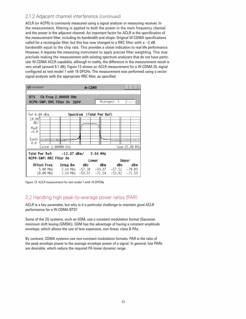
CCDF curves can help in several situations:
– to determine the headroom required when designing a component . – to confirm the power statistics of a given signal or stimulus . CCDF curves allow you to verify if the stimulus signal provided by another design team is adequate . For example, RF designers can use CCDF curves to verify that the signal provided by the digital signal processing (DSP) section is realistic .
– to confirm that a component design is adequate or to troubleshoot your subsystem or system design . You can make CCDF measurements at several points in a system . For example, if the ACLR of a transmitter is too high, you can make CCDF measurements at the input and output of the PA . If the PA design is correct, the curves coincide . If the PA compresses the signal, the PAR of the signal is lower at the output of the PA (Figure 15) .
Figure 15. CCDFs for test model 1 with 16 code channels with and without compression
Test model 1 with 16 DPCHsSignal at amplifier input
Test model 1 with 16 DPCHs Signal at amplifier output . Signal compressed .
2.2 Handling high peak-to-average power ratios (PAR) (continued)
25

QPSK transmitter
Codingframing
interleaving EVM
bitSymbol
Measurement
Reference
QPSKMOD
Idealbits
Rootraisedcosine
Rootraisedcosine
QPSKENCODER
Rootraisedcosine
QPSKENCODE
Rootraisedcosine
QPSKDECODE
I/Qrecovery
Q
I
Magnitude error(I/Q error magnitude)
Measuredsignal
Ideal signal(reference)
Phase error(I/Q error phase)
Error vector
ø
2.3 Measuring modulation accuracy In constant amplitude modulation schemes, such as GMSK, the phase and the frequency error are the metrics for modulation quality . However, these metrics are not very effective for non-constant amplitude modulation formats, which can also have errors in amplitude .
The accuracy of non-constant amplitude modulation schemes, such as quadrature amplitude modulation (QAM), or quadrature phase shift keying (QPSK), can be assessed very effectively by look-ing at the constellation of the signal . Signal impairment can be objectively assessed by taking the displacement of each measured symbol from the reference position as an error phasor (or vector), as shown in Figure 16 .
Figure 16. Error vector and related parameters
The reference position is determined from a reference signal that is synthesized by demodulating the data bits from the received signal and then re-modulating these bits “perfectly”, for a generic QPSK signal, as shown in Figure 17 .
Figure 17. Process to calculate EVM for a generic QPSK signal
The root mean square (RMS) of the error vectors is computed and expressed as a percentage of the square root of the mean power of the ideal signal1 . This is the error vector magnitude (EVM) . EVM is a common modulation quality metric widely used in digital communication systems .
When we consider evaluating the modulation accuracy of W-CDMA it becomes evident that this explanation of EVM, while sufficient for ordinary QPSK or QAM, needs further elaboration . Shall we measure the EVM at the chip or at the symbol level? Shall we measure EVM for a signal with a single DPDCH channel or with another channel configuration? How do we calculate the reference?
1. The actual calculation method of the percentage depends on the specific standard. The EVM may be normalized to the amplitude of the outermost sym-bol, the square root of the average symbol power, or the square root of the mean power of the ideal signal. In the case of W-CDMA, the specifications require normalization to the square root of the mean power of the ideal signal (see section on Composite EVM).
26
The following sections explain the differences between the various EVM and other modulation quality measurements that you can perform on a W-CDMA DL signal and when they should be used .
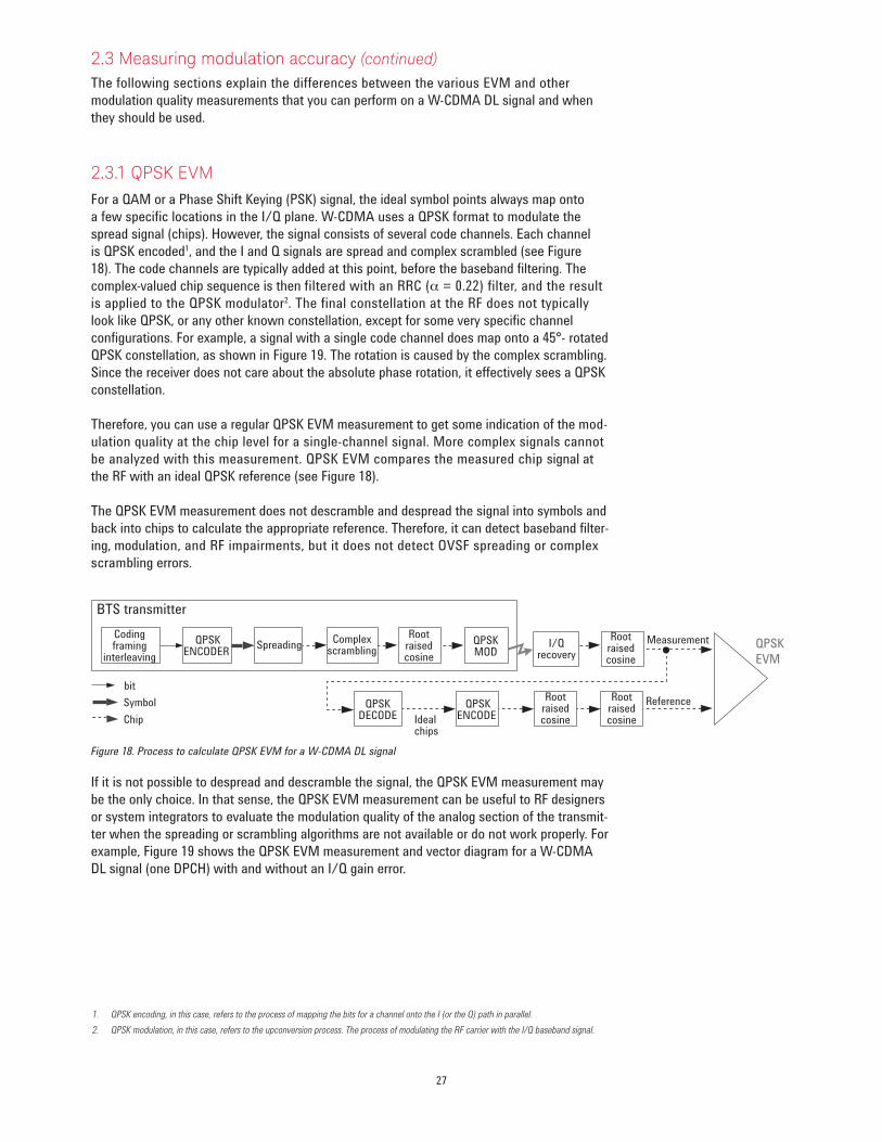
2.3.1 QPSK EVMFor a QAM or a Phase Shift Keying (PSK) signal, the ideal symbol points always map onto a few specific locations in the I/Q plane . W-CDMA uses a QPSK format to modulate the spread signal (chips) . However, the signal consists of several code channels . Each channel is QPSK encoded1, and the I and Q signals are spread and complex scrambled (see Figure 18) . The code channels are typically added at this point, before the baseband filtering . The complex-valued chip sequence is then filtered with an RRC (α = 0 .22) filter, and the result is applied to the QPSK modulator2 . The final constellation at the RF does not typically look like QPSK, or any other known constellation, except for some very specific channel configurations . For example, a signal with a single code channel does map onto a 45°- rotated QPSK constellation, as shown in Figure 19 . The rotation is caused by the complex scrambling . Since the receiver does not care about the absolute phase rotation, it effectively sees a QPSK constellation .
Therefore, you can use a regular QPSK EVM measurement to get some indication of the mod-ulation quality at the chip level for a single-channel signal . More complex signals cannot be analyzed with this measurement . QPSK EVM compares the measured chip signal at the RF with an ideal QPSK reference (see Figure 18) .
The QPSK EVM measurement does not descramble and despread the signal into symbols and back into chips to calculate the appropriate reference . Therefore, it can detect baseband filter-ing, modulation, and RF impairments, but it does not detect OVSF spreading or complex scrambling errors .
Figure 18. Process to calculate QPSK EVM for a W-CDMA DL signal
If it is not possible to despread and descramble the signal, the QPSK EVM measurement may be the only choice . In that sense, the QPSK EVM measurement can be useful to RF designers or system integrators to evaluate the modulation quality of the analog section of the transmit-ter when the spreading or scrambling algorithms are not available or do not work properly . For example, Figure 19 shows the QPSK EVM measurement and vector diagram for a W-CDMA DL signal (one DPCH) with and without an I/Q gain error .
BTS transmitter
QPSK EVM
bit
ChipSymbol
Measurement
Reference
I/Qrecovery
Idealchips
Codingframing
interleavingQPSK
ENCODER QPSKMODSpreading
Rootraisedcosine
Complexscrambling
Rootraisedcosine
Rootraisedcosine
QPSKENCODE
Rootraisedcosine
QPSKDECODE
1. QPSK encoding, in this case, refers to the process of mapping the bits for a channel onto the I (or the Q) path in parallel.2. QPSK modulation, in this case, refers to the upconversion process. The process of modulating the RF carrier with the I/Q baseband signal.
2.3 Measuring modulation accuracy (continued)
27
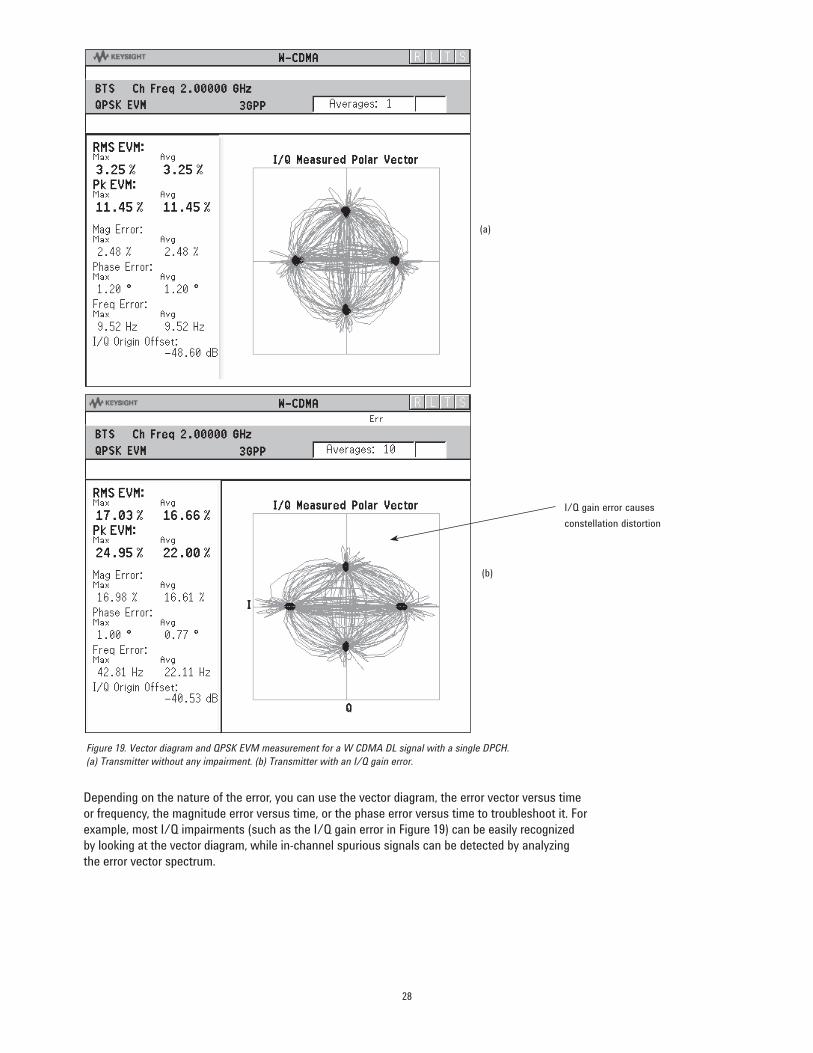
Depending on the nature of the error, you can use the vector diagram, the error vector versus time or frequency, the magnitude error versus time, or the phase error versus time to troubleshoot it . For example, most I/Q impairments (such as the I/Q gain error in Figure 19) can be easily recognized by looking at the vector diagram, while in-channel spurious signals can be detected by analyzing the error vector spectrum .
Figure 19. Vector diagram and QPSK EVM measurement for a W CDMA DL signal with a single DPCH. (a) Transmitter without any impairment. (b) Transmitter with an I/Q gain error.
I/Q gain error causes constellation distortion
(a)
(b)
28
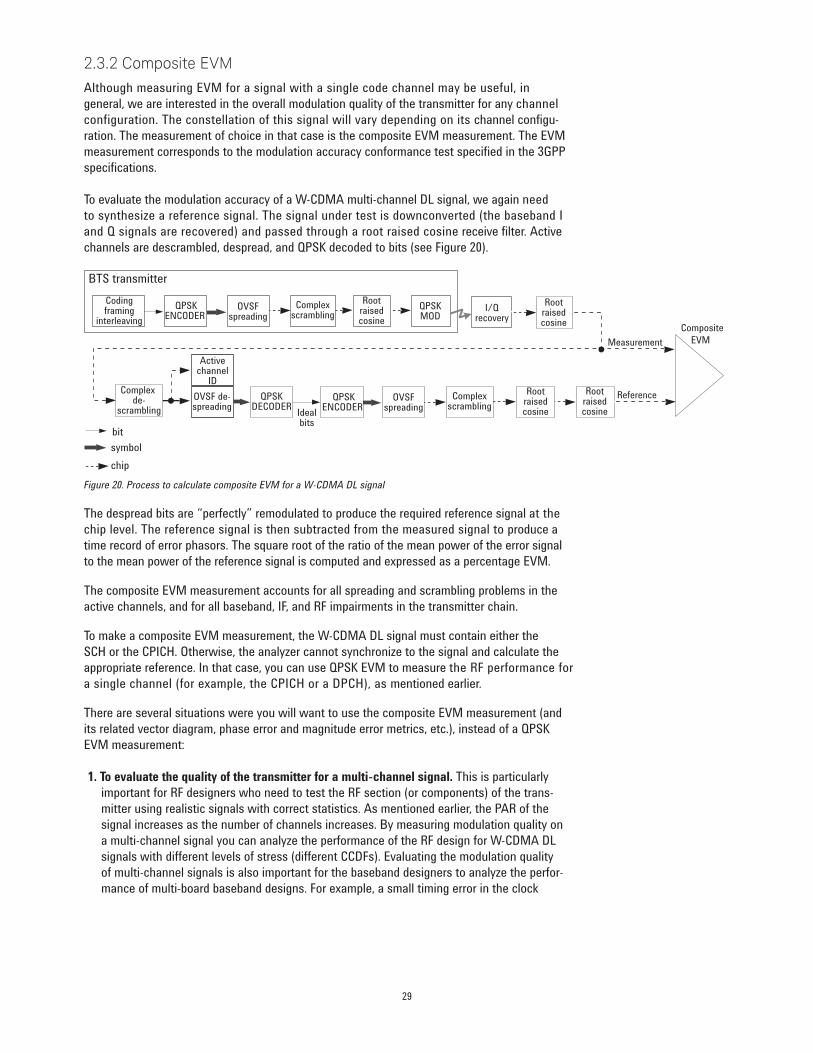
2.3.2 Composite EVM Although measuring EVM for a signal with a single code channel may be useful, in general, we are interested in the overall modulation quality of the transmitter for any channel configuration . The constellation of this signal will vary depending on its channel configu-ration . The measurement of choice in that case is the composite EVM measurement . The EVM measurement corresponds to the modulation accuracy conformance test specified in the 3GPP specifications .
To evaluate the modulation accuracy of a W-CDMA multi-channel DL signal, we again need to synthesize a reference signal . The signal under test is downconverted (the baseband I and Q signals are recovered) and passed through a root raised cosine receive filter . Active channels are descrambled, despread, and QPSK decoded to bits (see Figure 20) .
Figure 20. Process to calculate composite EVM for a W-CDMA DL signal
The despread bits are “perfectly” remodulated to produce the required reference signal at the chip level . The reference signal is then subtracted from the measured signal to produce a time record of error phasors . The square root of the ratio of the mean power of the error signal to the mean power of the reference signal is computed and expressed as a percentage EVM .
The composite EVM measurement accounts for all spreading and scrambling problems in the active channels, and for all baseband, IF, and RF impairments in the transmitter chain .
To make a composite EVM measurement, the W-CDMA DL signal must contain either the SCH or the CPICH . Otherwise, the analyzer cannot synchronize to the signal and calculate the appropriate reference . In that case, you can use QPSK EVM to measure the RF performance for a single channel (for example, the CPICH or a DPCH), as mentioned earlier .
There are several situations were you will want to use the composite EVM measurement (and its related vector diagram, phase error and magnitude error metrics, etc .), instead of a QPSK EVM measurement:
1. To evaluate the quality of the transmitter for a multi-channel signal. This is particularly important for RF designers who need to test the RF section (or components) of the trans-mitter using realistic signals with correct statistics . As mentioned earlier, the PAR of the signal increases as the number of channels increases . By measuring modulation quality on a multi-channel signal you can analyze the performance of the RF design for W-CDMA DL signals with different levels of stress (different CCDFs) . Evaluating the modulation quality of multi-channel signals is also important for the baseband designers to analyze the perfor-mance of multi-board baseband designs . For example, a small timing error in the clock
Composite EVM
bit
chipsymbol
Complexscrambling
OVSF de-spreading Ideal
bits
QPSKDECODER
BTS transmitter
Measurement
Reference
I/Qrecovery
Codingframing
interleavingQPSKMOD
OVSFspreading
Rootraisedcosine
Complexscrambling
Rootraisedcosine
Rootraisedcosine
QPSKENCODER
Complex de-
scramblingOVSF
spreadingQPSK
ENCODER
Rootraisedcosine
Activechannel
ID
29

synchronization between channels on different boards can be detected as a decrease in mod-ulation quality . The channel configuration required in the specifications for the EVM modulation quality conformance test is provided by test model 4 . Test model 4 consists of the P-CCPCH, the SCH, and optionally, the CPICH . Figure 21(a) shows the vector diagram and composite EVM measurement for test model 4 (P-CCPCH and SCH), as required by the specifications . However, to obtain a more meaningful measure of the modulation quality for a real life DL signal, the composite EVM measurement should be performed on a signal with multiple channels, as shown in Figure 21(b) for a signal with the P-CCPCH, SCH, CPICH, and 32 DPCHs .
2. To detect spreading or scrambling errors. Depending on the degree of the error, the analyzer
may show an intermittent unlock condition or may not be able to lock at all when trying to per-form a composite EVM measurement . This is mainly useful to system integrators to determine errors in the spreading and scrambling . If this problem occurs, the QPSK EVM measurement can be used to confirm that the rest of the transmitter is working as expected . If the scrambling or spreading error does not cause an unlock measurement condition, the error vector versus time display can be used to find the problematic chip .
3. To detect certain problems between the baseband and RF sections. This is mainly useful for system integrators . For example, local oscillator (LO) instability caused by interference from digital signals can be detected with QPSK EVM . However, the QPSK EVM measure-ment will not detect problems that require the measurement to synchronize with a bit sequence . For example, I/Q swapped (reversed I and Q) errors will look perfectly normal if a QPSK EVM measurement is used . Conversely, it will cause an unlock condition when performing a composite EVM measurement .
Figure 21. Vector diagram and composite EVM measurement for a W CDMA DL signal with (a) the P CCPCH/SCH, and (b) the P CCPCH/SCH, CPICH, and 32 DPCHs.
(a)
(b)
Composite EVM
2.3.2 Composite EVM (continued)
30
Composite EVM is useful throughout the development, performance verification, and manu-facturing phases of the BTS life cycle as a single figure of merit of the composite waveform as a whole . However code-by-code composition of the multiplex is also of interest . The primary means of investigating this is to look at the distribution of power in the code domain .
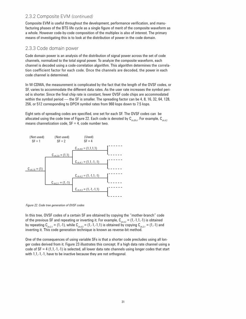
2.3.3 Code domain powerCode domain power is an analysis of the distribution of signal power across the set of code channels, normalized to the total signal power . To analyze the composite waveform, each channel is decoded using a code-correlation algorithm . This algorithm determines the correla-tion coefficient factor for each code . Once the channels are decoded, the power in each code channel is determined .
In W-CDMA, the measurement is complicated by the fact that the length of the OVSF codes, or SF, varies to accommodate the different data rates . As the user rate increases the symbol peri-od is shorter . Since the final chip rate is constant, fewer OVSF code chips are accommodated within the symbol period — the SF is smaller . The spreading factor can be 4, 8, 16, 32, 64, 128, 256, or 512 corresponding to DPCH symbol rates from 960 ksps down to 7 .5 ksps .
Eight sets of spreading codes are specified, one set for each SF . The OVSF codes can be allocated using the code tree of Figure 22 . Each code is denoted by Cch,SF,n . For example, Cch,4,2 means channelization code, SF = 4, code number two .
In this tree, OVSF codes of a certain SF are obtained by copying the “mother-branch” code of the previous SF and repeating or inverting it . For example, Cch,4,2 = (1,-1,1,-1) is obtained by repeating Cch,2,1 = (1,-1), while Cch,4,3 = (1,-1,-1,1) is obtained by copying Cch,2,1 = (1,-1) and inverting it . This code generation technique is known as reverse-bit method .
One of the consequences of using variable SFs is that a shorter code precludes using all lon-ger codes derived from it . Figure 23 illustrates this concept . If a high data rate channel using a code of SF = 4 (1,1,-1,-1) is selected, all lower data rate channels using longer codes that start with 1,1,-1,-1, have to be inactive because they are not orthogonal .
(Not used)SF = 1
(Not used)SF = 2
(Used)SF = 4
C ch,1,0 = (1)
C ch,2,0 = (1,1)
C ch,2,1 = (1,-1)
C ch,4,0 = (1,1,1,1)
C ch,4,1 = (1,1,-1,-1)
C ch,4,2 = (1,-1,1,-1)
C ch,4,3 = (1,-1,-1,1)
Figure 22. Code tree generation of OVSF codes
2.3.2 Composite EVM (continued)
31
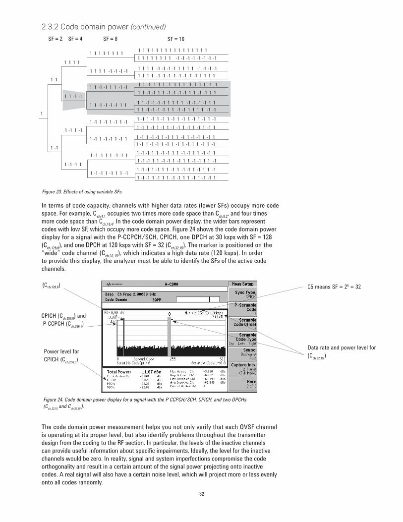
In terms of code capacity, channels with higher data rates (lower SFs) occupy more code space . For example, Cch,4,1 occupies two times more code space than Cch,8,2, and four times more code space than Cch,16,4 . In the code domain power display, the wider bars represent codes with low SF, which occupy more code space . Figure 24 shows the code domain power display for a signal with the P-CCPCH/SCH, CPICH, one DPCH at 30 ksps with SF = 128 (Cch,128,8), and one DPCH at 120 ksps with SF = 32 (Cch,32,15) . The marker is positioned on the “wide” code channel (Cch,32,15), which indicates a high data rate (120 ksps) . In order to provide this display, the analyzer must be able to identify the SFs of the active code channels .
The code domain power measurement helps you not only verify that each OVSF channel is operating at its proper level, but also identify problems throughout the transmitter design from the coding to the RF section . In particular, the levels of the inactive channels can provide useful information about specific impairments . Ideally, the level for the inactive channels would be zero . In reality, signal and system imperfections compromise the code orthogonality and result in a certain amount of the signal power projecting onto inactive codes . A real signal will also have a certain noise level, which will project more or less evenly onto all codes randomly .
CPICH (Cch,256,0) and P CCPCH (Cch,256,1)
Data rate and power level for(Cch,32,15 )
C5 means SF = 25 = 32
Power level for CPICH (Cch,256,0)
(Cch,128,8)
Figure 24. Code domain power display for a signal with the P CCPCH/SCH, CPICH, and two DPCHs (Cch,32,15
and Cch,32,15 ).
SF = 16SF = 2 SF = 4 SF = 8
1 1 1 1 1 1 1 1
1 1 1 1 -1 -1 -1 -1
1 1 -1 -1
1 1 1 1
1 1
1 -1
1 -1 1 -1
1 -1 -1 1
1
1 -1 1 -1 1 -1 1 -1
1 -1 1 -1 -1 1 -1 1
1 -1 -1 1 1 -1 -1 1
1 -1 -1 1 -1 1 1 -1
1 1 -1 -1 -1 -1 1 1
1 1 -1 -1 1 1 -1 -1
1 1 1 1 1 1 1 1 1 1 1 1 1 1 1 1
1 1 1 1 1 1 1 1 -1 -1 -1 -1 -1 -1 -1 -1
1 1 1 1 -1 -1 -1 -1 1 1 1 1 -1 -1 -1 -1
1 1 1 1 -1 -1 -1 -1 -1 -1 -1 -1 1 1 1 1
1 1 -1 -1 1 1 -1 -1 1 1 -1 -1 1 1 -1 -1
1 1 -1 -1 1 1 -1 -1 -1 -1 1 1 -1 -1 1 1
1 1 -1 -1 -1 -1 1 1 1 1 -1 -1 -1 -1 1 1
1 1 -1 -1 -1 -1 1 1 -1 -1 1 1 1 1 -1 -1
1 -1 1 -1 1 -1 1 -1 1 -1 1 -1 1 -1 1 -1
1 -1 1 -1 1 -1 1 -1 -1 1 -1 1 -1 1 -1 1
1 -1 1 -1 -1 1 -1 1 1 -1 1 -1 -1 1 -1 1
1 -1 1 -1 -1 1 -1 1 -1 1 -1 1 1 -1 1 -1
1 -1 -1 1 1 -1 -1 1 1 -1 -1 1 1 -1 -1 1
1 -1 -1 1 1 -1 -1 1 -1 1 1 -1 -1 1 1 -1
1 -1 -1 1 -1 1 1 -1 1 -1 -1 1 -1 1 1 -1
1 -1 -1 1 -1 1 1 -1 -1 1 1 -1 1 -1 -1 1
Figure 23. Effects of using variable SFs
2.3.2 Code domain power (continued)
32
The projection of the error is interesting because it enables us to see how the error power is distributed in the code domain . You want the error power to be evenly distributed throughout the code domain, rather than concentrated in a few codes, to avoid code-dependent channel quality variations .
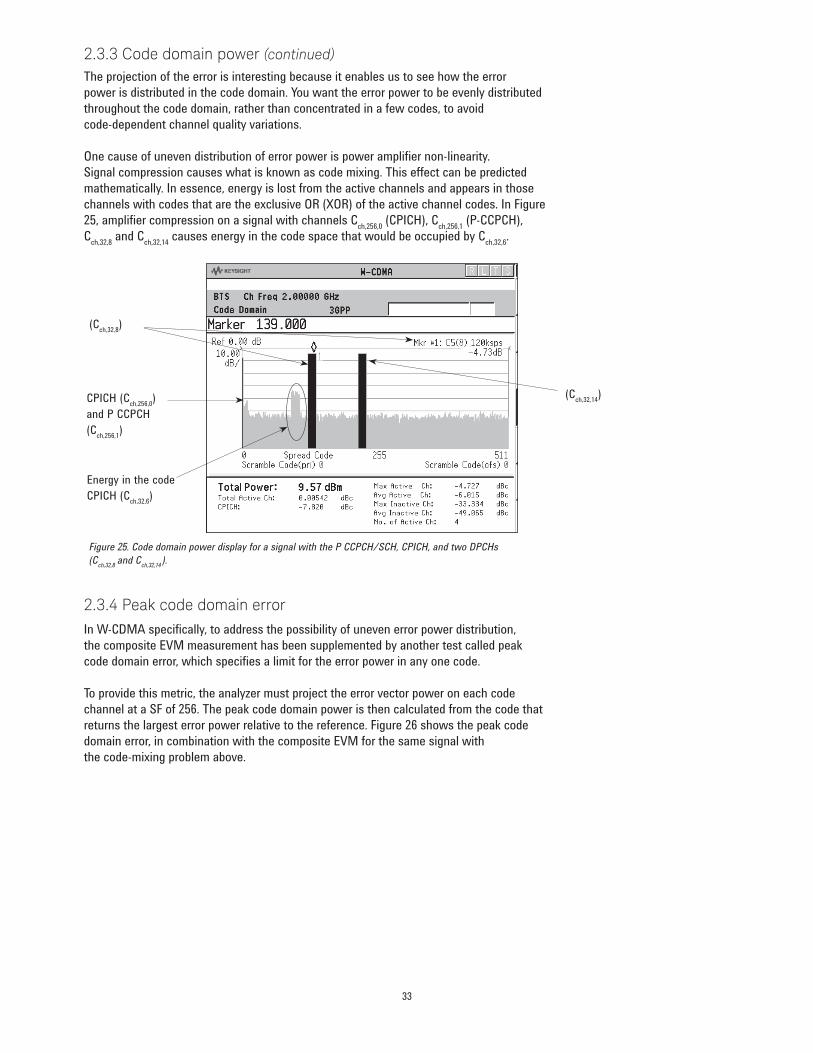
One cause of uneven distribution of error power is power amplifier non-linearity . Signal compression causes what is known as code mixing . This effect can be predicted mathematically . In essence, energy is lost from the active channels and appears in those channels with codes that are the exclusive OR (XOR) of the active channel codes . In Figure 25, amplifier compression on a signal with channels Cch,256,0 (CPICH), Cch,256,1 (P-CCPCH), Cch,32,8 and Cch,32,14 causes energy in the code space that would be occupied by Cch,32,6 .
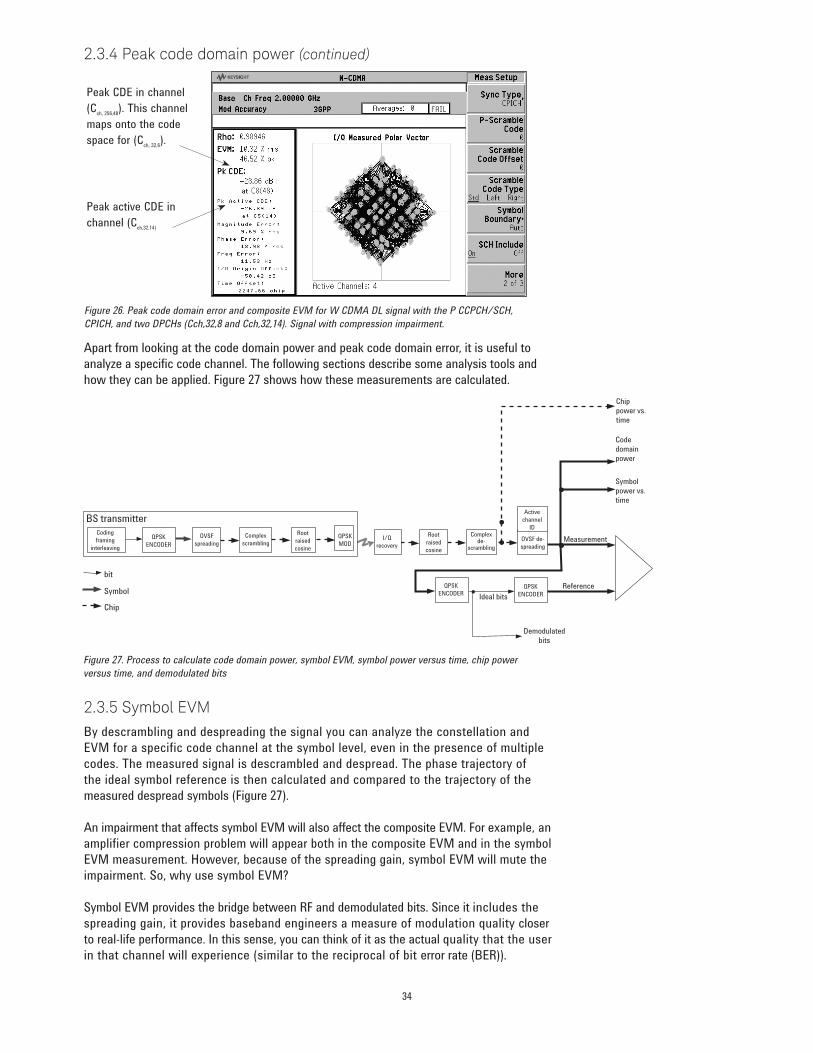
2.3.4 Peak code domain errorIn W-CDMA specifically, to address the possibility of uneven error power distribution, the composite EVM measurement has been supplemented by another test called peak code domain error, which specifies a limit for the error power in any one code .
To provide this metric, the analyzer must project the error vector power on each code channel at a SF of 256 . The peak code domain power is then calculated from the code that returns the largest error power relative to the reference . Figure 26 shows the peak code domain error, in combination with the composite EVM for the same signal with the code-mixing problem above .
Figure 25. Code domain power display for a signal with the P CCPCH/SCH, CPICH, and two DPCHs (Cch,32,8 and Cch,32,14 ).
CPICH (Cch,256,0) and P CCPCH (Cch,256,1)
Energy in the code CPICH (Cch,32,6)
(Cch,32,8)
(Cch,32,14)
2.3.3 Code domain power (continued)
33
Apart from looking at the code domain power and peak code domain error, it is useful to analyze a specific code channel . The following sections describe some analysis tools and how they can be applied . Figure 27 shows how these measurements are calculated .
Figure 27. Process to calculate code domain power, symbol EVM, symbol power versus time, chip power versus time, and demodulated bits
2.3.5 Symbol EVM By descrambling and despreading the signal you can analyze the constellation and EVM for a specific code channel at the symbol level, even in the presence of multiple codes . The measured signal is descrambled and despread . The phase trajectory of the ideal symbol reference is then calculated and compared to the trajectory of the measured despread symbols (Figure 27) .
An impairment that affects symbol EVM will also affect the composite EVM . For example, an amplifier compression problem will appear both in the composite EVM and in the symbol EVM measurement . However, because of the spreading gain, symbol EVM will mute the impairment . So, why use symbol EVM?
Symbol EVM provides the bridge between RF and demodulated bits . Since it includes the spreading gain, it provides baseband engineers a measure of modulation quality closer to real-life performance . In this sense, you can think of it as the actual quality that the user in that channel will experience (similar to the reciprocal of bit error rate (BER)) .
Peak CDE in channel (Cch, 256,48) . This channel maps onto the code space for (Cch, 32,6) .
Peak active CDE in channel (Cch,32,14)
Figure 26. Peak code domain error and composite EVM for W CDMA DL signal with the P CCPCH/SCH, CPICH, and two DPCHs (Cch,32,8 and Cch,32,14). Signal with compression impairment.
BS transmitterCodingframing
interleaving
QPSKENCODER
OVSFspreading
Complexscrambling
Rootraisedcosine
bit
Chip
Symbol
Measurement
Reference
I/Qrecovery
QPSKMOD
Ideal bits
OVSF de-spreading
Complexde-
scrambling
Activechannel
ID
Demodulatedbits
Code domain power
Symbol power vs. time
Chippower vs.time
Rootraisedcosine
QPSKENCODER
QPSKENCODER
2.3.4 Peak code domain power (continued)
34
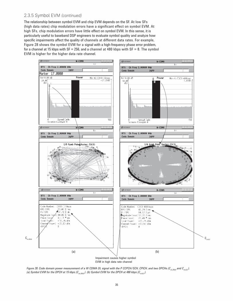
The relationship between symbol EVM and chip EVM depends on the SF . At low SFs (high data rates) chip modulation errors have a significant effect on symbol EVM . At high SFs, chip modulation errors have little effect on symbol EVM . In this sense, it is particularly useful to baseband DSP engineers to evaluate symbol quality and analyze how specific impairments affect the quality of channels at different data rates . For example, Figure 28 shows the symbol EVM for a signal with a high-frequency phase error problem, for a channel at 15 kbps with SF = 256, and a channel at 480 kbps with SF = 8 . The symbol EVM is higher for the higher data rate channel .
Figure 28. Code domain power measurement of a W CDMA DL signal with the P CCPCH/SCH, CPICH, and two DPCHs (Cch,256,8 and Cch,8,3 ). (a) Symbol EVM for the DPCH at 15 kbps (Cch,256,8 ). (b) Symbol EVM for the DPCH at 480 kbps (Cch,8,3 ).
Cch,8,3Cch,256,8
(b)(a)
Impairment causes higher symbolEVM in high data rate channel
2.3.5 Symbol EVM (continued)
35
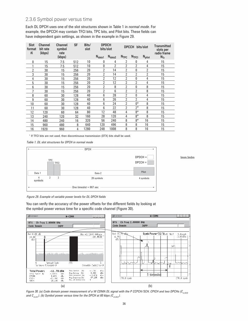
2.3.6 Symbol power versus timeEach DL DPCH uses one of the slot structures shown in Table 1 in normal mode . For example, the DPCCH may contain TFCI bits, TPC bits, and Pilot bits . These fields can have independent gain settings, as shown in the example in Figure 29 .
Slot Channel Channel SF Bits/ DPDCH DPCCH bits/slot format bit rate symbol slot bits/slot #i (kbps) rate (kbps) 0 15 7.5 512 1 15 7.5 512 2 30 15 256 3 30 15 256 4 30 15 256 5 30 15 256 6 30 15 256 7 30 15 256 8 60 30 128 9 60 30 128 10 60 30 128 11 60 30 128 12 120 60 64 13 240 120 32 14 480 240 16 15 960 480 8 16 1920 960 4
Ndata1 Ndata2 NTPC NTFCI Npilot
0 4 2 0 4 0 2 2 2 4 2 14 2 0 2 2 14 2 2 2 2 12 2 0 4 2 12 2 2 4 2 8 2 0 8 2 6 2 2 8 6 28 2 0 4 6 26 2 2 4 6 24 2 0 8 6 22 2 2 8 12 48 4 8 8 28 120 4 8 8 56 240 8 8 16 120 496 8 8 16 248 1008 8 8 16
10102020202020204040404080
160320640
1280
1515151515151515151515151515151515
Transmittedslots per
radio frameNTr
*****
Table 1. DL slot structures for DPCH in normal mode
DPCCH =DPDCH =
28 symbols
TFCI
24
Data 1
2Data 2
TPC
symbols
Pilot
4 symbols
One timeslot = 667 sec
DPCH
Figure 29. Example of variable power levels for DL DPCH fields
Figure 30. (a) Code domain power measurement of a W CDMA DL signal with the P CCPCH/SCH, CPICH and two DPCHs (Cch,64,8 and Cch,8,4 ). (b) Symbol power versus time for the DPCH at 60 kbps (Cch,64,8 ).
(b)(a)
You can verify the accuracy of the power offsets for the different fields by looking at the symbol power versus time for a specific code channel (Figure 30) .
1 timeslot
* If TFCI bits are not used, then discontinuous transmission (DTX) bits shall be used .
lmm .lmlm
36

The symbol power versus time measurement can be used to monitor the power and response of the BTS power control system . Averaging the symbol power over one time- slot provides the code domain power for the code channel . Code domain power is the recommended method to perform the power control steps conformance test that requires measuring the accuracy of the power steps of a particular code channel as a response to a series of power control commands .
Figure 31 shows the despread symbol power in combination with the composite (total) chip power for a DL signal . Chip power represents the total power of the signal at the chip rate . Analyzing the symbol power for a channel in combination with the total chip power versus time is particularly useful for system integrators to analyze the power amplifier response (ripple) to power offsets or to a power control command .
2.3.7 Demodulated bitsBy obtaining the demodulated symbols after descrambling and despreading for each code channel, the correct symbol patterns can be verified . As shown in Table 1, the DL DPCCH can have different slot structures . You can verify if the bits for the different fields (Pilot, TFCI, TPC, etc .) are correct by using the demodulated bits measurement (Figure 32) .
Demodulated bits is an important troubleshooting tool for baseband engineers to identify coding and interleaving errors . In many cases, it can help you clarify situations where the BTS and UE are having problems communicating with each other . Analyzing the demodulated bits may verify whether the error is coming from the BTS coding and interleaving or the UE de-interleaving and decoding process .
Figure 32. Code domain power measurement of a W CDMA DL signal with the P CCPCH/SCH, CPICH, and two DPCHs(Cch,64,8 and Cch,8,4) and symbol power versus time coupled with demodulated bits for the DPCH at 60 kbps(Cch,64,8).
4 slots
Figure 31. Chip power versus time for a signal with the P CCPCH/SCH, CPICH, and two DPCHs(Cch,64,8 and Cch,8,4) and symbol power versus time for the channel at 60 kbps(Cch,64,8)
Composite chip power versus time
Symbol power versus time for Cch,64,8
2.3.6 Symbol power versus time (continued)
37
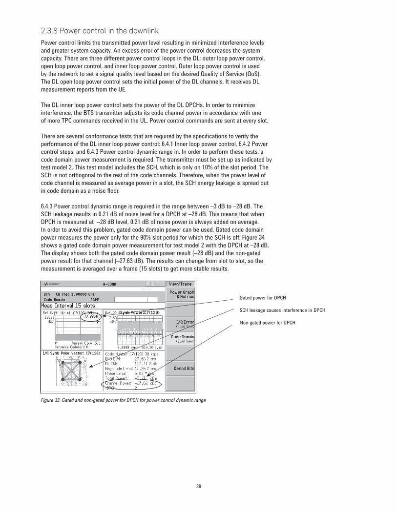
2.3.8 Power control in the downlinkPower control limits the transmitted power level resulting in minimized interference levels and greater system capacity . An excess error of the power control decreases the system capacity . There are three different power control loops in the DL: outer loop power control, open loop power control, and inner loop power control . Outer loop power control is used by the network to set a signal quality level based on the desired Quality of Service (QoS) . The DL open loop power control sets the initial power of the DL channels . It receives DL measurement reports from the UE .
The DL inner loop power control sets the power of the DL DPCHs . In order to minimize interference, the BTS transmitter adjusts its code channel power in accordance with one of more TPC commands received in the UL . Power control commands are sent at every slot .
There are several conformance tests that are required by the specifications to verify the performance of the DL inner loop power control: 6 .4 .1 Inner loop power control, 6 .4 .2 Power control steps, and 6 .4 .3 Power control dynamic range in . In order to perform these tests, a code domain power measurement is required . The transmitter must be set up as indicated by test model 2 . This test model includes the SCH, which is only on 10% of the slot period . The SCH is not orthogonal to the rest of the code channels . Therefore, when the power level of code channel is measured as average power in a slot, the SCH energy leakage is spread out in code domain as a noise floor .
6 .4 .3 Power control dynamic range is required in the range between –3 dB to –28 dB . The SCH leakage results in 0 .21 dB of noise level for a DPCH at –28 dB . This means that when DPCH is measured at –28 dB level, 0 .21 dB of noise power is always added on average . In order to avoid this problem, gated code domain power can be used . Gated code domain power measures the power only for the 90% slot period for which the SCH is off . Figure 34 shows a gated code domain power measurement for test model 2 with the DPCH at –28 dB . The display shows both the gated code domain power result (–28 dB) and the non-gated power result for that channel (–27 .63 dB) . The results can change from slot to slot, so the measurement is averaged over a frame (15 slots) to get more stable results .
Figure 33. Gated and non-gated power for DPCH for power control dynamic range
Gated power for DPCH
SCH leakage causes interference in DPCH
Non-gated power for DPCH
38
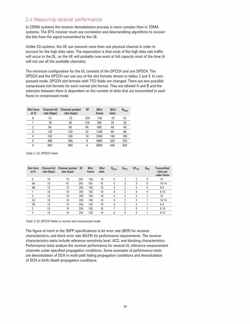
2.4 Measuring receiver performanceIn CDMA systems the receiver demodulation process is more complex than in TDMA systems . The BTS receiver must use correlation and descrambling algorithms to recover the bits from the signal transmitted by the UE .
Unlike 2G systems, the UE can transmit more than one physical channel in order to account for the high data rates . The expectation is that most of the high data rate traffic will occur in the DL, so the UE will probably now work at full capacity most of the time (it will not use all the available channels) .
The minimum configuration for the UL consists of the DPCCH and one DPDCH . The DPDCH and the DPCCH can use any of the slot formats shown in tables 2 and 3 . In com-pressed mode, DPCCH slot formats with TFCI fields are changed . There are two possible compressed slot formats for each normal slot format . They are labeled A and B and the selection between them is dependent on the number of slots that are transmitted in each frame in compressed mode .
Table 2. UL DPDCH fields
Table 3. UL DPCCH fields in normal and compressed mode
The figure of merit in the 3GPP specifications is bit error rate (BER) for receiver characteristics, and block error rate (BLER) for performance requirements . The receiver characteristics tests include reference sensitivity level, ACS, and blocking characteristics . Performance tests analyze the receiver performance for several UL reference measurement channels under specified propagation conditions . Some examples of performance tests are demodulation of DCH in multi-path fading propagation conditions and demodulation of DCH in birth/death propagation conditions .
Slot form Channel bit Channel symbol SF Bits/ Bits/ Npilot NTPC NTFCI NFBI Transmitted at #i rate (kbps) rate (ksps) frame slots slots per radio frame 0 15 15 256 150 10 6 2 2 0 15 0A 15 15 256 150 10 5 2 3 0 10-14 0B 15 15 256 150 10 4 2 4 0 8-9 1 15 15 256 150 10 8 2 0 0 8-15 2 15 15 256 150 10 5 2 2 1 15 2A 15 15 256 150 10 4 2 3 1 10-14 2B 15 15 256 150 10 3 2 4 1 8-9 3 15 15 256 150 10 7 2 0 1 8-15 4 15 15 256 150 10 6 4 0 1 8-15
Slot form Channel bit Channel symbol SF Bits/ Bits/ Ndata at #i rate (kbps) rate (ksps) frame slots 0 15 15 256 150 10 10 1 30 30 128 300 20 20 2 60 60 64 600 40 40 3 120 120 32 1200 80 80 4 240 240 16 2400 160 160 5 480 480 8 4800 320 320 6 960 960 4 9600 640 640
39
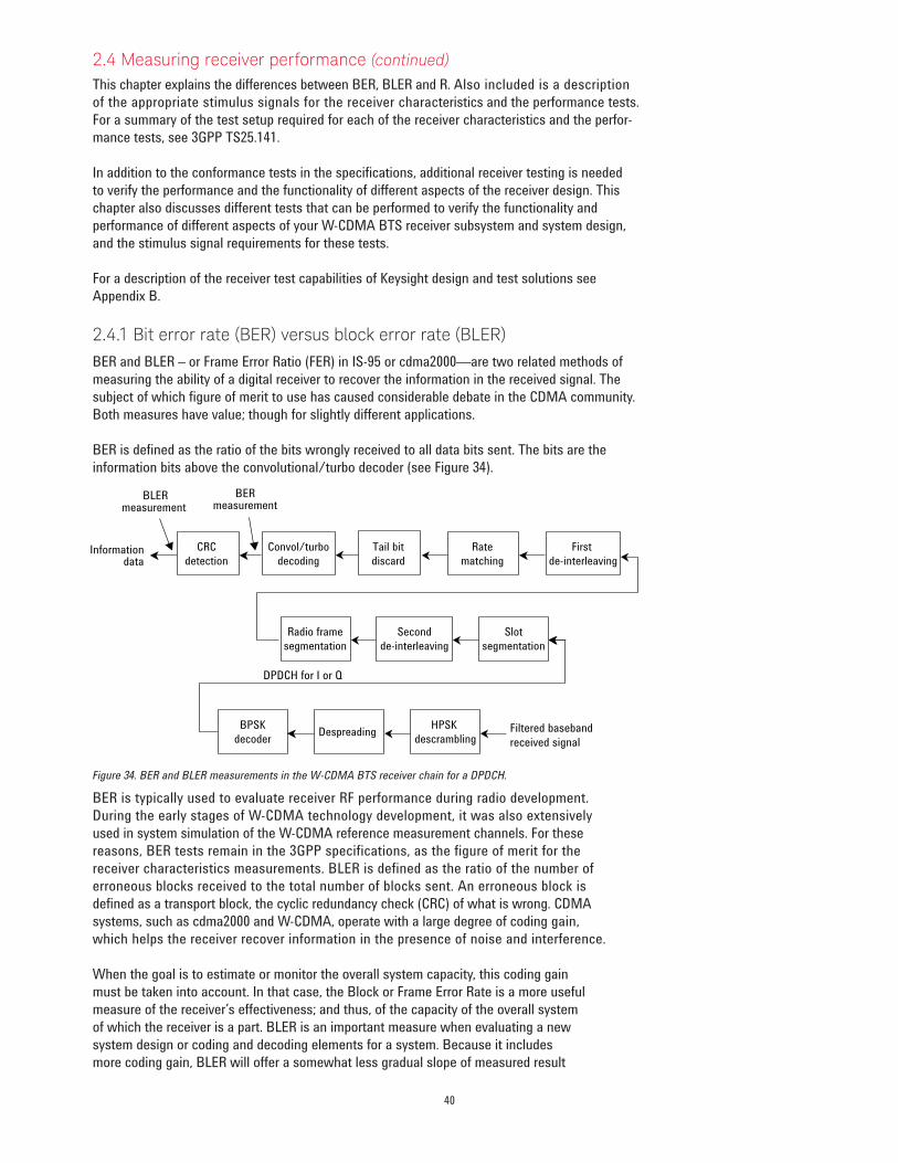
This chapter explains the differences between BER, BLER and R . Also included is a description of the appropriate stimulus signals for the receiver characteristics and the performance tests . For a summary of the test setup required for each of the receiver characteristics and the perfor-mance tests, see 3GPP TS25 .141 .
In addition to the conformance tests in the specifications, additional receiver testing is needed to verify the performance and the functionality of different aspects of the receiver design . This chapter also discusses different tests that can be performed to verify the functionality and performance of different aspects of your W-CDMA BTS receiver subsystem and system design, and the stimulus signal requirements for these tests .
For a description of the receiver test capabilities of Keysight design and test solutions see Appendix B .
2.4.1 Bit error rate (BER) versus block error rate (BLER)BER and BLER – or Frame Error Ratio (FER) in IS-95 or cdma2000—are two related methods of measuring the ability of a digital receiver to recover the information in the received signal . The subject of which figure of merit to use has caused considerable debate in the CDMA community . Both measures have value; though for slightly different applications .
BER is defined as the ratio of the bits wrongly received to all data bits sent . The bits are the information bits above the convolutional/turbo decoder (see Figure 34) .
Figure 34. BER and BLER measurements in the W-CDMA BTS receiver chain for a DPDCH.
BER is typically used to evaluate receiver RF performance during radio development . During the early stages of W-CDMA technology development, it was also extensively used in system simulation of the W-CDMA reference measurement channels . For these reasons, BER tests remain in the 3GPP specifications, as the figure of merit for the receiver characteristics measurements . BLER is defined as the ratio of the number of erroneous blocks received to the total number of blocks sent . An erroneous block is defined as a transport block, the cyclic redundancy check (CRC) of what is wrong . CDMA systems, such as cdma2000 and W-CDMA, operate with a large degree of coding gain, which helps the receiver recover information in the presence of noise and interference .
When the goal is to estimate or monitor the overall system capacity, this coding gain must be taken into account . In that case, the Block or Frame Error Rate is a more useful measure of the receiver’s effectiveness; and thus, of the capacity of the overall system of which the receiver is a part . BLER is an important measure when evaluating a new system design or coding and decoding elements for a system . Because it includes more coding gain, BLER will offer a somewhat less gradual slope of measured result
BER measurement
CRCdetection
Convol/turbodecoding
Ratematching
First de-interleaving
Radio framesegmentation
Slotsegmentation
Secondde-interleaving
Information data
DPDCH for I or Q
BLER measurement
Tail bitdiscard
BPSKdecoder
HPSK descramblingDespreading Filtered baseband
received signal
2.4 Measuring receiver performance (continued)
40
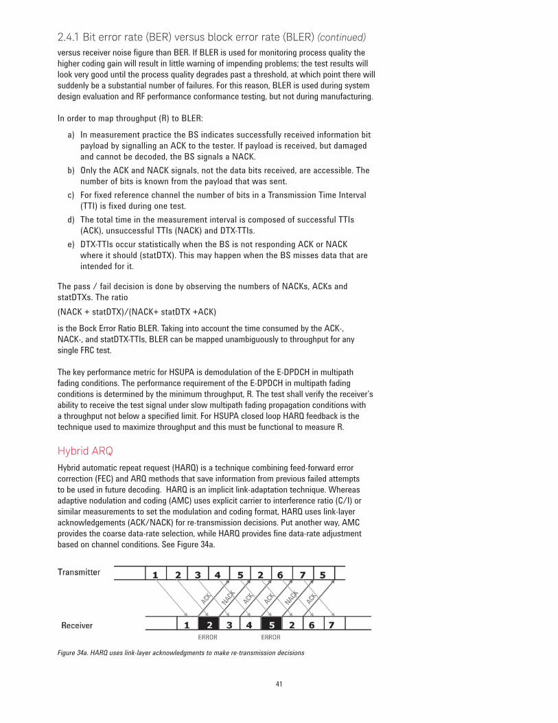
versus receiver noise figure than BER . If BLER is used for monitoring process quality the higher coding gain will result in little warning of impending problems; the test results will look very good until the process quality degrades past a threshold, at which point there will suddenly be a substantial number of failures . For this reason, BLER is used during system design evaluation and RF performance conformance testing, but not during manufacturing .
In order to map throughput (R) to BLER:
a) In measurement practice the BS indicates successfully received information bit payload by signalling an ACK to the tester . If payload is received, but damaged and cannot be decoded, the BS signals a NACK .
b) Only the ACK and NACK signals, not the data bits received, are accessible . The number of bits is known from the payload that was sent .
c) For fixed reference channel the number of bits in a Transmission Time Interval (TTI) is fixed during one test .
d) The total time in the measurement interval is composed of successful TTIs (ACK), unsuccessful TTIs (NACK) and DTX-TTIs .
e) DTX-TTIs occur statistically when the BS is not responding ACK or NACK where it should (statDTX) . This may happen when the BS misses data that are intended for it .
The pass / fail decision is done by observing the numbers of NACKs, ACKs and statDTXs . The ratio (NACK + statDTX)/(NACK+ statDTX +ACK)
is the Bock Error Ratio BLER . Taking into account the time consumed by the ACK-, NACK-, and statDTX-TTIs, BLER can be mapped unambiguously to throughput for any single FRC test .
The key performance metric for HSUPA is demodulation of the E-DPDCH in multipath fading conditions . The performance requirement of the E-DPDCH in multipath fading conditions is determined by the minimum throughput, R . The test shall verify the receiver’s ability to receive the test signal under slow multipath fading propagation conditions with a throughput not below a specified limit . For HSUPA closed loop HARQ feedback is the technique used to maximize throughput and this must be functional to measure R .
Hybrid ARQHybrid automatic repeat request (HARQ) is a technique combining feed-forward error correction (FEC) and ARQ methods that save information from previous failed attempts to be used in future decoding . HARQ is an implicit link-adaptation technique . Whereas adaptive nodulation and coding (AMC) uses explicit carrier to interference ratio (C/I) or similar measurements to set the modulation and coding format, HARQ uses link-layer acknowledgements (ACK/NACK) for re-transmission decisions . Put another way, AMC provides the coarse data-rate selection, while HARQ provides fine data-rate adjustment based on channel conditions . See Figure 34a .
Figure 34a. HARQ uses link-layer acknowledgments to make re-transmission decisions
2.4.1 Bit error rate (BER) versus block error rate (BLER) (continued)
41
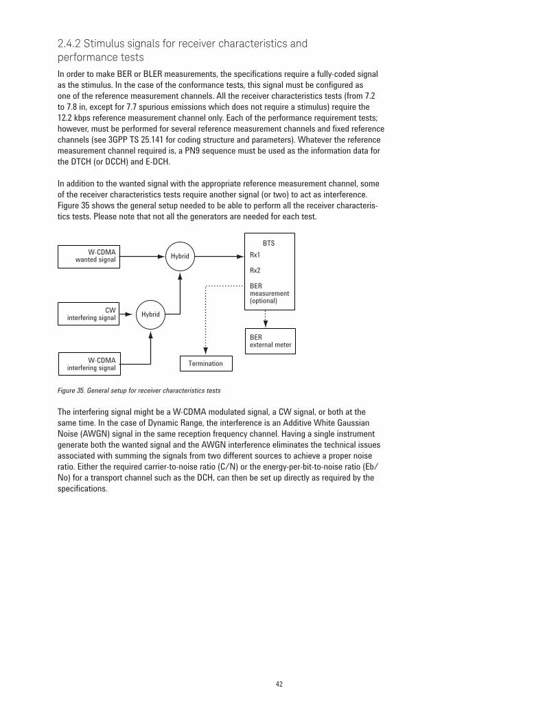
2.4.2 Stimulus signals for receiver characteristics and performance tests In order to make BER or BLER measurements, the specifications require a fully-coded signal as the stimulus . In the case of the conformance tests, this signal must be configured as one of the reference measurement channels . All the receiver characteristics tests (from 7 .2 to 7 .8 in, except for 7 .7 spurious emissions which does not require a stimulus) require the 12 .2 kbps reference measurement channel only . Each of the performance requirement tests; however, must be performed for several reference measurement channels and fixed reference channels (see 3GPP TS 25 .141 for coding structure and parameters) . Whatever the reference measurement channel required is, a PN9 sequence must be used as the information data for the DTCH (or DCCH) and E-DCH .
In addition to the wanted signal with the appropriate reference measurement channel, some of the receiver characteristics tests require another signal (or two) to act as interference . Figure 35 shows the general setup needed to be able to perform all the receiver characteris-tics tests . Please note that not all the generators are needed for each test .
Figure 35. General setup for receiver characteristics tests
The interfering signal might be a W-CDMA modulated signal, a CW signal, or both at the same time . In the case of Dynamic Range, the interference is an Additive White Gaussian Noise (AWGN) signal in the same reception frequency channel . Having a single instrument generate both the wanted signal and the AWGN interference eliminates the technical issues associated with summing the signals from two different sources to achieve a proper noise ratio . Either the required carrier-to-noise ratio (C/N) or the energy-per-bit-to-noise ratio (Eb/No) for a transport channel such as the DCH, can then be set up directly as required by the specifications .
W-CDMAwanted signal Hybrid
CWinterfering signal Hybrid
W-CDMAinterfering signal
Rx1
Rx2
BERmeasurement(optional)
BERexternal meter
Termination
BTS
42
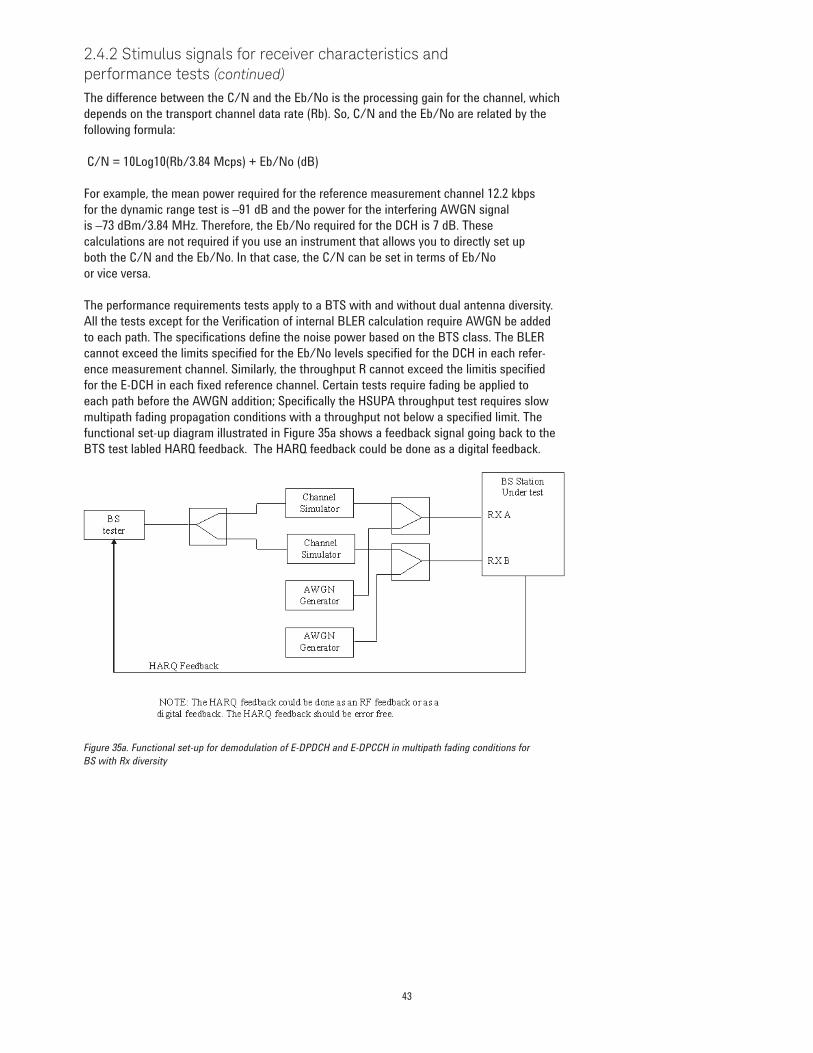
The difference between the C/N and the Eb/No is the processing gain for the channel, which depends on the transport channel data rate (Rb) . So, C/N and the Eb/No are related by the following formula:
C/N = 10Log10(Rb/3 .84 Mcps) + Eb/No (dB)
For example, the mean power required for the reference measurement channel 12 .2 kbps for the dynamic range test is –91 dB and the power for the interfering AWGN signal is –73 dBm/3 .84 MHz . Therefore, the Eb/No required for the DCH is 7 dB . These calculations are not required if you use an instrument that allows you to directly set up both the C/N and the Eb/No . In that case, the C/N can be set in terms of Eb/No or vice versa .
The performance requirements tests apply to a BTS with and without dual antenna diversity . All the tests except for the Verification of internal BLER calculation require AWGN be added to each path . The specifications define the noise power based on the BTS class . The BLER cannot exceed the limits specified for the Eb/No levels specified for the DCH in each refer-ence measurement channel . Similarly, the throughput R cannot exceed the limitis specified for the E-DCH in each fixed reference channel . Certain tests require fading be applied to each path before the AWGN addition; Specifically the HSUPA throughput test requires slow multipath fading propagation conditions with a throughput not below a specified limit . The functional set-up diagram illustrated in Figure 35a shows a feedback signal going back to the BTS test labled HARQ feedback . The HARQ feedback could be done as a digital feedback .
Figure 35a. Functional set-up for demodulation of E-DPDCH and E-DPCCH in multipath fading conditions for BS with Rx diversity
2.4.2 Stimulus signals for receiver characteristics and performance tests (continued)
43
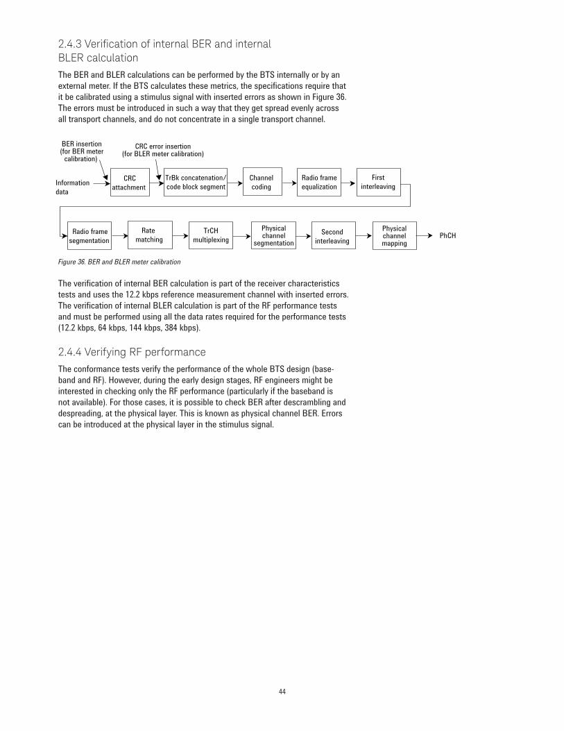
2.4.3 Verification of internal BER and internal BLER calculationThe BER and BLER calculations can be performed by the BTS internally or by an external meter . If the BTS calculates these metrics, the specifications require that it be calibrated using a stimulus signal with inserted errors as shown in Figure 36 . The errors must be introduced in such a way that they get spread evenly across all transport channels, and do not concentrate in a single transport channel .
Figure 36. BER and BLER meter calibration
The verification of internal BER calculation is part of the receiver characteristics tests and uses the 12 .2 kbps reference measurement channel with inserted errors . The verification of internal BLER calculation is part of the RF performance tests and must be performed using all the data rates required for the performance tests (12 .2 kbps, 64 kbps, 144 kbps, 384 kbps) .
2.4.4 Verifying RF performanceThe conformance tests verify the performance of the whole BTS design (base-band and RF) . However, during the early design stages, RF engineers might be interested in checking only the RF performance (particularly if the baseband is not available) . For those cases, it is possible to check BER after descrambling and despreading, at the physical layer . This is known as physical channel BER . Errors can be introduced at the physical layer in the stimulus signal .
BER insertion(for BER meter
calibration)
CRCattachment
Radio frameequalization
Physicalchannelmapping
Informationdata
CRC error insertion(for BLER meter calibration)
Channelcoding
Secondinterleaving
TrBk concatenation/code block segment
Radio framesegmentation
Rate matching
Firstinterleaving
Physicalchannel
segmentationTrCH
multiplexing PhCH
44
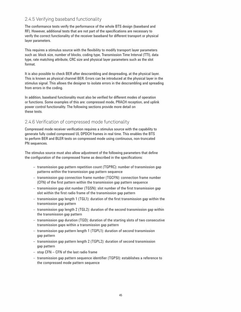
2.4.5 Verifying baseband functionalityThe conformance tests verify the performance of the whole BTS design (baseband and RF) . However, additional tests that are not part of the specifications are necessary to verify the correct functionality of the receiver baseband for different transport or physical layer parameters .
This requires a stimulus source with the flexibility to modify transport layer parameters such as: block size, number of blocks, coding type, Transmission Time Interval (TTI), data type, rate matching attribute, CRC size and physical layer parameters such as the slot format .
It is also possible to check BER after descrambling and despreading, at the physical layer . This is known as physical channel BER . Errors can be introduced at the physical layer in the stimulus signal . This allows the designer to isolate errors in the descrambling and spreading from errors in the coding .
In addition, baseband functionality must also be verified for different modes of operation or functions . Some examples of this are: compressed mode, PRACH reception, and uplink power control functionality . The following sections provide more detail on these tests .
2.4.6 Verification of compressed mode functionalityCompressed mode receiver verification requires a stimulus source with the capability to generate fully coded compressed UL DPDCH frames in real time . This enables the BTS to perform BER and BLER tests on compressed mode using continuous, non-truncated PN sequences .
The stimulus source must also allow adjustment of the following parameters that define the configuration of the compressed frame as described in the specifications:
– transmission gap pattern repetition count (TGPRC): number of transmission gap patterns within the transmission gap pattern sequence
– transmission gap connection frame number (TGCFN): connection frame number (CFN) of the first pattern within the transmission gap pattern sequence
– transmission gap slot number (TGSN): slot number of the first transmission gap slot within the first radio frame of the transmission gap pattern
– transmission gap length 1 (TGL1): duration of the first transmission gap within the transmission gap pattern
– transmission gap length 2 (TGL2): duration of the second transmission gap within the transmission gap pattern
– transmission gap duration (TGD): duration of the starting slots of two consecutive transmission gaps within a transmission gap pattern
– transmission gap pattern length 1 (TGPL1): duration of second transmission gap pattern
– transmission gap pattern length 2 (TGPL2): duration of second transmission gap pattern
– stop CFN – CFN of the last radio frame – transmission gap pattern sequence identifier (TGPSI): establishes a reference to the compressed mode pattern sequence
45
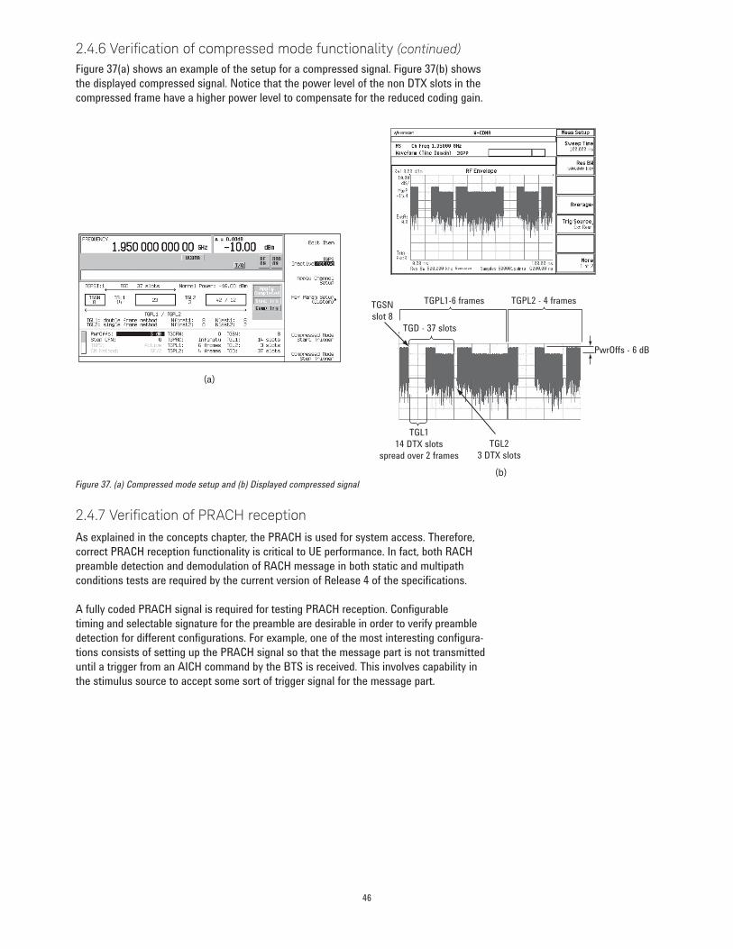
Figure 37(a) shows an example of the setup for a compressed signal . Figure 37(b) shows the displayed compressed signal . Notice that the power level of the non DTX slots in the compressed frame have a higher power level to compensate for the reduced coding gain .
Figure 37. (a) Compressed mode setup and (b) Displayed compressed signal
2.4.7 Verification of PRACH receptionAs explained in the concepts chapter, the PRACH is used for system access . Therefore, correct PRACH reception functionality is critical to UE performance . In fact, both RACH preamble detection and demodulation of RACH message in both static and multipath conditions tests are required by the current version of Release 4 of the specifications .
A fully coded PRACH signal is required for testing PRACH reception . Configurable timing and selectable signature for the preamble are desirable in order to verify preamble detection for different configurations . For example, one of the most interesting configura-tions consists of setting up the PRACH signal so that the message part is not transmitted until a trigger from an AICH command by the BTS is received . This involves capability in the stimulus source to accept some sort of trigger signal for the message part .
TGL114 DTX slots
spread over 2 framesTGL2
3 DTX slots
TGSNslot 8
TGPL1-6 frames
TGD - 37 slots
PwrOffs - 6 dB
TGPL2 - 4 frames
(a)
(b)
2.4.6 Verification of compressed mode functionality (continued)
46
Testing PRACH reception under multiple PRACH transmission is also necessary to verify the ability of the BTS to detect PRACHs from different UEs . This requires a source capable of simulating multiple UEs attempting to contact a BTS . Particularly interesting is overloading testing with multiple PRACHs . This might required more than one signal source, each transmitting multiple PRACHs . Figure 38(a) shows an access slot setup for a signal with three preambles (notice that UE3 is off) . Figure 38(b) shows the displayed three-PRACH signal .
Figure 38. (a) Access slot setup and timing for multiple PRACHs and (b) Transmitted multiple PRACH signal.
2.4.8 Verification of uplink power controlThe BTS can always minimize the transmission power against the required quality at the receiver by transmitting TPC commands based on SIR measurements . This maximizes total system capacity . Power control at each slot is needed to keep the received signal quality constant under fading conditions .
Verifying the BTS real-time power control function (the BTS capability to appropriately measure receiver SIR and generate TPC commands accordingly) requires the signal source to simulate the UE by generating a signal that changes its power upon reception of different input levels that correspond to TPC commands from the BTS .
Message part for UE1, UE2and UE4 added together
Remaining UE2 message part
UE1 second PRACH transmission
Preamble for UE2
Preamble for UE1and UE4 added together
Message part for UE1and UE4 added together
(b)
(a)
2.4.7 Verification of PRACH reception (continued)
47

3. Special Considerations for Femtocells
As service providers begin mass deployment of femtocells, manufacturers face unprecedented challenges to deliver quality, low-cost devices to market . Femtocells are subject to 3GPP’s rigorous verification and conformance documents, as well as stringent new requirements on interference and compatibility with the broader network where they are used . During development, the same measurements as described above will be used, though the specification limits may be different in some cases due to the lower output power of the device . Designers must also be aware that achieving cost goals comparable with Wireless LAN access points will be a huge challenge in manu-facturing, and one of the main drivers will be the way the product is initially designed .
While a normal network base station will have assigned operating parameters and be installed by a dedicated team of engineers, femtocells are designed to be switched on and operated by anyone, and must work without causing network problems (See Figure 39) . Therefore, in addition to typical functionality, they must include simple turn-on procedures and continuous monitoring of the network environment for self-organizing operating frequencies, codes and handovers between the device and the network . To facilitate this, the femtocell may have a “sniffer” – essentially a simplified UE receiver – to allow it to search for base stations and other femtocells operating locally and to determine the scrambling codes they are using . This implies the need for a separate set of receiver tests to verify the sniffer functions correctly .
Figure 39. Typical network implementation with femtocell management
Global Positioning System (GPS) is yet another component which will become increasingly important in the femtocell, enabling location assistance for emergency (E911) calls, timing and frequency assistance to provide system clock functionality, and a location licensing capability . With its adoption into the femtocell, verification of GPS functionality has become an increasingly important task . It also offers a way to make the femtocell smart enough so that it can avoid interfering with existing infrastructure and can only be used within the geographical area for which the network operator has a license .
48
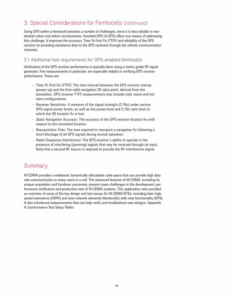
3. Special Considerations for Femtocells (continued)
Using GPS within a femtocell presents a number of challenges, since it is less reliable in resi-dential/urban and indoor environments . Assisted GPS (A-GPS) offers one means of addressing this challenge . It improves the accuracy, Time To First Fix (TTFF) and reliability of the GPS receiver by providing assistance data to the GPS receivers through the cellular communication channels .
3.1 Additional test requirements for GPS-enabled femtocells Verification of the GPS receiver performance is typically done using a metric-grade RF signal generator . Five measurements in particular, are especially helpful in verifying GPS receiver performance . These are:
– Time To First Fix (TTFF): The time interval between the GPS receiver startup (power up) and the first-valid navigation 3D-data point, derived from the simulation . GPS receiver TTFF measurements may include cold, warm and hot start configurations .
– Receiver Sensitivity: A measure of the signal strength (C/No) under various GPS-signal power levels, as well as the power level and C/No ratio level at which the 3D location fix is lost .
– Static Navigation Accuracy: The accuracy of the GPS receiver location fix with respect to the simulated location .
– Reacquisition Time: The time required to reacquire a navigation fix following a short blockage of all GPS signals during normal operation .
– Radio-Frequency Interference: The GPS receiver’s ability to operate in the presence of interfering (jamming) signals that may be received through its input . Note that a second RF source is required to provide the RF interference signal .
Summary
W-CDMA provides a wideband, dynamically allocatable code space that can provide high data rate communication to many users in a cell . The advanced features of W-CDMA, including its unique acquisition and handover processes, present many challenges in the development, per-formance verification and production test of W-CDMA systems . This application note provided an overview of some of the key design and test issues for W-CDMA BTSs, including later high-speed extensions (HSPA) and new network elements (femtocells) with new functionality (GPS) . It also introduced measurements that can help verify and troubleshoot new designs . Appendix A: Conformance Test Setup Tables
49
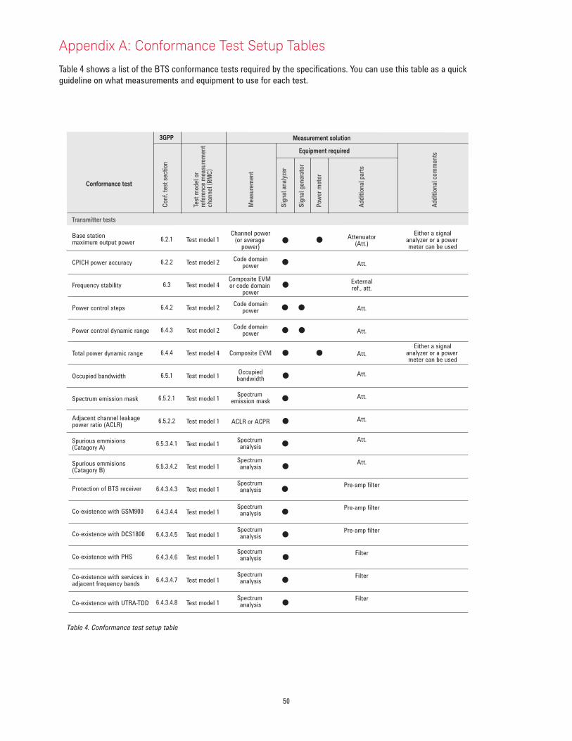
Appendix A: Conformance Test Setup Tables
Table 4 shows a list of the BTS conformance tests required by the specifications . You can use this table as a quick guideline on what measurements and equipment to use for each test .
Transmitter tests
Base stationmaximum output power
CPICH power accuracy
Frequency stability
Power control steps
Power control dynamic range
Total power dynamic range
Occupied bandwidth
Spectrum emission mask
Adjacent channel leakage power ratio (ACLR)
Spurious emmisions (Catagory A)
Spurious emmisions (Catagory B)
Protection of BTS receiver
Co-existence with GSM900
Co-existence with DCS1800
Co-existence with PHS
Co-existence with services in adjacent frequency bands
Co-existence with UTRA-TDD
6.2.1
6.2.2
6.3
6.4.2
6.4.3
6.4.4
6.5.1
6.5.2.1
6.5.2.2
6.5.3.4.1
6.5.3.4.2
6.4.3.4.3
6.4.3.4.4
6.4.3.4.5
6.4.3.4.6
6.4.3.4.7
6.4.3.4.8
Test model 1
Test model 2
Test model 4
Test model 2
Test model 2
Test model 4
Test model 1
Test model 1
Test model 1
Test model 1
Test model 1
Test model 1
Test model 1
Test model 1
Test model 1
Test model 1
Test model 1
Channel power(or average
power)
Code domainpower
Composite EVM or code domain
powerCode domain
power
Code domainpower
Composite EVM
Occupiedbandwidth
Spectrum emission mask
ACLR or ACPR
Spectrum analysis
Spectrum analysis
Spectrum analysis
Spectrum analysis
Spectrum analysis
Spectrum analysis
Spectrum analysis
Spectrum analysis
Attenuator(Att.)
Att.
Externalref., att.
Att.
Att.
Att.
Att.
Att.
Att.
Att.
Att.
Pre-amp filter
Pre-amp filter
Pre-amp filter
Filter
Filter
Filter
Either a signalanalyzer or a power meter can be used
Either a signalanalyzer or a power meter can be used
Conf
. tes
t sec
tion
Test
mod
el o
rre
fere
nce
mea
sure
men
tch
anne
l (RM
C)
Mea
sure
men
t
Sign
al a
naly
zer
Sign
al g
ener
ator
Equipment required
Conformance test
Measurement solution3GPP
Pow
er m
eter
Addi
tiona
l com
men
ts
Addi
tiona
l par
ts
Table 4. Conformance test setup table
50
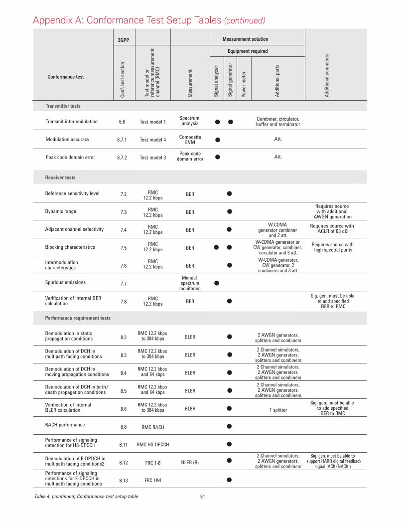
7.2
7.3
7.4
7.5
7.6
7.7
7.8
8.2
8.3
8.4
8.5
8.6
8.8
8.11
8.12
8.13
RMC12.2 kbps
RMC12.2 kbps
RMC12.2 kbps
RMC12.2 kbps
RMC12.2 kbps
RMC12.2 kbps
RMC 12.2 kbps to 384 kbps
RMC 12.2 kbps to 384 kbps
RMC 12.2 kbps and 64 kbps
RMC 12.2 kbps and 64 kbps
RMC 12.2 kbps to 384 kbps
RMC RACH
RMC HS-DPCCH
FRC 1-8
FRC 1&4
BER
BER
BER
BER
BER
Manual spectrum
monitoring
BER
BLER
BLER
BLER
BLER
BLER
BLER (R)
W-CDMA generator combiner
and 2 att.W-CDMA generator or
CW generator, combiner, circulator and 3 att.W-CDMA generator,
CW generator, 2combiners and 3 att.
2 AWGN generators,splitters and combiners2 Channel simulators,2 AWGN generators,
splitters and combiners2 Channel simulators,2 AWGN generators,
splitters and combiners2 Channel simulators,2 AWGN generators,
splitters and combiners
1 splitter
2 Channel simulators,2 AWGN generators,
splitters and combiners
Sig. gen. must be able to add specified
BER to RMC
Requires source with high spectral purity
Sig. gen. must be able to add specified
BER to RMC
Sig. gen. must be able to support HARQ digital feedback
signal (ACK/NACK )
Receiver tests
Reference sensitivity level
Dynamic range
Adjacent channel selectivity
Blocking characteristics
Intermodulationcharacteristics
Spurious emissions
Verification of internal BERcalculation
Performance requirement tests
Demodulation in static propagation conditions
Demodulation of DCH in multipath fading conditions
Demodulation of DCH in moving propagation conditions
Demodulation of DCH in birth/death propagation conditions
Verification of internal BLER calculation
RACH performance
Performance of signaling detection for HS-DPCCH
Demodulation of E-DPDCH in multipath fading conditions2Performance of signaling detections for E-DPCCH in multipath fading conditions
Equipment required
Measurement solution
Conf
. tes
t sec
tion
Test
mod
el o
rre
fere
nce
mea
sure
men
tch
anne
l (RM
C)
Mea
sure
men
t
Sign
al a
naly
zer
Sign
al g
ener
ator
Conformance test
3GPP
Pow
er m
eter
Addi
tiona
l com
men
ts
Addi
tiona
l par
ts
6.6
6.7.1
6.7.2
Test model 1
Test model 4
Test model 3
Spectrum analysis
CompositeEVM
Peak codedomain error
Combiner, circulator, buffer and terminator
Att.
Att.
Transmitter tests
Requires source with ACLR of 63 dB
Requires source with additional
AWGN generation
Transmit intermodulation
Modulation accuracy
Peak code domain error
Appendix A: Conformance Test Setup Tables (continued)
Table 4. (continued) Conformance test setup table 51
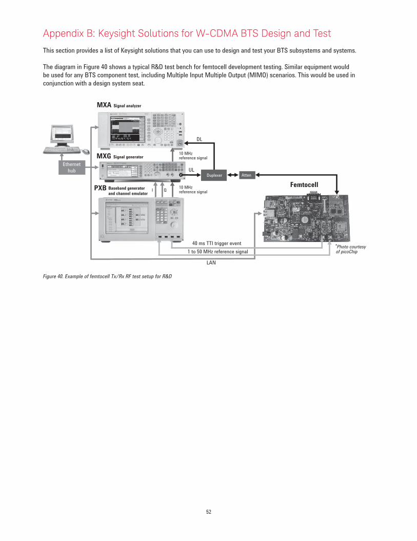
40 ms TTI trigger event 1 to 50 MHz reference signal
UL
DL
Atten
Femtocell
MXA Signal analyzer
MXG Signal generatorEthernet
hub
PXB Baseband generator and channel emulator
10 MHz reference signal
10 MHz reference signal
QI
LAN
Duplexer
*Photo courtesy of picoChip
Appendix B: Keysight Solutions for W-CDMA BTS Design and Test
This section provides a list of Keysight solutions that you can use to design and test your BTS subsystems and systems .
The diagram in Figure 40 shows a typical R&D test bench for femtocell development testing . Similar equipment would be used for any BTS component test, including Multiple Input Multiple Output (MIMO) scenarios . This would be used in conjunction with a design system seat .
Figure 40. Example of femtocell Tx/Rx RF test setup for R&D
52
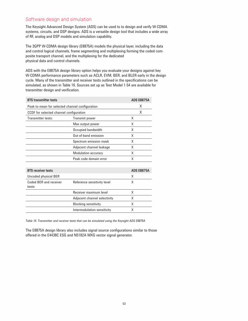
Software design and simulationThe Keysight Advanced Design System (ADS) can be used to to design and verify W-CDMA systems, circuits, and DSP designs . ADS is a versatile design tool that includes a wide array of RF, analog and DSP models and simulation capability .
The 3GPP W-CDMA design library (E8875A) models the physical layer, including the data and control logical channels, frame segmenting and multiplexing forming the coded com-posite transport channel, and the multiplexing for the dedicated physical data and control channels .
ADS with the E8875A design library option helps you evaluate your designs against key W-CDMA performance parameters such as ACLR, EVM, BER, and BLER early in the design cycle . Many of the transmitter and receiver tests outlined in the specifications can be simulated, as shown in Table 16 . Sources set up as Test Model 1-54 are available for transmitter design and verification .
Table 16. Transmitter and receiver tests that can be simulated using the Keysight ADS E8875A
The E8875A design library also includes signal source configurations similar to those offered in the E4438C ESG and N5182A MXG vector signal generator .
BTS transmitter tests ADS E8875A
XX
Transmitter tests: Transmit power XMax output power XOccupied bandwidth XOut-of-band emission XSpectrum emission mask XAdjacent channel leakage XModulation accuracy XPeak code domain error X
BTS receiver tests ADS E8875A
Uncoded physical BER XCoded BER and receiver tests:
Reference sensitivity level X
Receiver maximum level XAdjacent channel selectivity XBlocking sensitivity XIntermodulation sensitivity X
Peak-to-mean for selected channel configurationCCDF for selected channel configuration
53

Connected solutionsConnectivity between Keysight ADS and Keysight test equipment, such as signal sources and signal analyzers, helps minimize develop ment risk and costs by identifying problems early in the design and fabrication cycle .
W-CDMA system designers can benefit from connected solutions because it can help:
– evaluate system-level performance with partial RF hardware, using simulation to model missing hardware .
– evaluate RF performance (such as BER), using simulation to model missing base-band functionality .
– evaluate system performance more continuously throughout the design/fabrica-tion cycle to help reduce risk and costs .
– evaluate system performance on the testbench with simulated impairments .
W-CDMA component designers benefit from connected solutions because they can use realistic signals for testing that reflect the environment in which the component will be used . Applications include:
– Testing/demonstrating a component DUT . Modeling a transmitter/receiver chain simulation to show how it would perform in a system .
– Testing/demonstrating a component with various signal formats modeled in simulation .
– Evaluating performance limits of a DUT – how impaired can the input signal be and still meet specifications?
Signal generation
Component testing
Signal creation software with the E4438C ESG, N5182A MXG and N5106A PXB simulates the 3GPP W-CDMA physical layer . These statistically correct signals are designed to stress W-CDMA handset components and subsystems, just as a real-world signal would . An easy to use interface enables you to:
– Select from several predefined W-CDMA channel configurations, including all the DL test models (1-6), including Home Node B (femtocell)
– Generate up to 32 carriers, for multicarrier component testing – Setup multicarrier clipping and timing offsets – Use the table editor to fully configure a W-CDMA multi-channel signal per your requirements
An easy-to-use interface link enables easy download custom waveforms created with ADS into ESG or MXG signal generators .
54
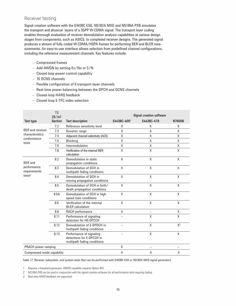
Receiver testingSignal creation software with the E4438C ESG, N5182A MXG and N5106A PXB simulates the transport and physical layers of a 3GPP W-CDMA signal . The transport layer coding enables thorough evaluation of receiver demodulation analysis capabilities at various design stages from components, such as ASICS, to completed receiver designs . The generated signal produces a stream of fully coded W-CDMA/HSPA frames for performing BER and BLER mea-surements . An easy-to-use interface allows selection from predefined channel configurations, including the reference measurement channels . Key features include:
– Compressed frames – Add AWGN by setting Ec/No or C/N – Closed loop power control capability – 16 OCNS channels – Flexible configuration of 6 transport layer channels – Real-time power balancing between the DPCH and OCNS channels – Closed-loop HARQ feedback – Closed-loop E-TFC index selection
TS 25.141 Signal creation software
Test type Section Test description E4438C-4001 E4438C-419 N7600B 7 .2 Reference sensitivity level X X X
7 .3 Dynamic range X X X7 .4 Adjacent channel selectivity (ACS) X X X7 .5 Blocking X X X7 .6 Intermodulation X X X7 .8 Verification of the internal BER
calculationX X X
8 .2 Demodulation in static propagation conditions
X X X
8 .3 Demodulation of DCH in multipath fading conditions
X X X
8 .4 Demodulation of DCH in moving propagation conditions
X X X
8 .5 Demodulation of DCH in birth/ death propagation conditions
X X X
8 .5A Demodulation of DCH in high speed train conditions
X X X
8 .6 Verification of the internal BLER calculation
X X X
8 .8 RACH performance X – X8 .11 Performance of signaling
detection for HS-DPCCH– X X
8 .12 Demodulation of E-DPDCH in multipath fading conditions
– X X3
8 .13 Performance of signaling detections for E-DPCCH in multipath fading conditions
– X X
PRACH power ramping X – –Compressed mode capability X X X
1. Requires a baseband generator. AWGN capability requires Option 403. 2. N5106A PXB can be used in conjunction with the signal creation software for all performance tests requiring fading.3. Real-time HARQ feedback not supported.
BER and receivercharacteristicsconformancetests
BER and performance requirements tests2
Table 17. Receiver subsystem, and system tests that can be performed with E4438C ESG or N5182A MXG signal generators
55

Power meters and sensors The Keysight EPM-P series power meters and E9320 peak and average power sensors provide peak, average and peak to average ratio power measurements on W-CDMA signals . Extensive triggering features are available for making time gated measurements . Fast test times, with a measurement speed of up to 1,000 corrected readings per second, over the GPIB, help increase throughput to meet time to market and time to volume goals . The E9320 peak and average power sensors have a maximum video bandwidth of 5 MHz, ideal for W-CDMA power measurements . High power measurements (average only) of up to 25 W (+44 dBm) are available in the E9300 series .
EPM-P analyzer software is provided with the EPM-P series power meters . This is a PC-based tool for pulse and statistical analysis on TDMA and CDMA modulation formats . For statistical analysis of the power distribution, the EPM-P analyzer software provides the capability to determine the probability density function (PDF), cumulative distri-bution function (CDF), and CCDF on W-CDMA signals .
Recommended power meters and sensors for 3GPP W-CDMA BTS peak, average and time gated power measurements are:
– EPM-P series power meter E4416A, single channel – EPM-P series power meter E4417A, dual channel – E9323A peak and average power sensor, 50 MHz to 6 GHz, 5 MHz video band-width, 60 to +20 dBm
All 8480 and E series power sensors are compatible with the EPM-P series power meters .
For average power measurements only, the lower cost EPM series power meters, U2000 Series USB power sensors and other E series power sensors recommended are:
– EPM series power meter N1913A, single channel – EPM series power meter N1914A, dual channel – U2001A USB power sensor, 10 MHz to 6 GHz, –60 to +20 dBm – U2001H USB power sensor, 10 MHz to 6 GHz, –50 to +30 dBm – U2001B USB power sensor, 10 MHz to 6 GHz, –30 to +44 dBm – E9301A power sensor, 10 MHz to 6 GHz, 60 to +20 dBm – E9301H power sensor, 10 MHz to 6 GHz, 50 to +30 dBm – E9301B power sensor, 10 MHz to 6 GHz, 30 to +44 dBm
Other power sensors in the 8480 series and N8480 series are compatible with the EPM series power meters .
For wide bandwidth power and time measurements, the P-series power meters and sensors provide peak, average, peak-to-average ratio power measurements, time-gated and free-run modes, rise and fall time and pulse width measurements . The range includes:
– EPM-P series power meter N1911A, single channel – EPM-P series power meter N1912A, dual channel – N1921A power sensor, 50 MHz to 18 GHz, –35 to +20 dBm – N1922A power sensor, 50 MHz to 40 GHz, –35 to +20 dBm
The 8480 and E-series power sensors are also compatible with the P-series power meters using adaptor cables . See the on-line configuration guide for details . .
56
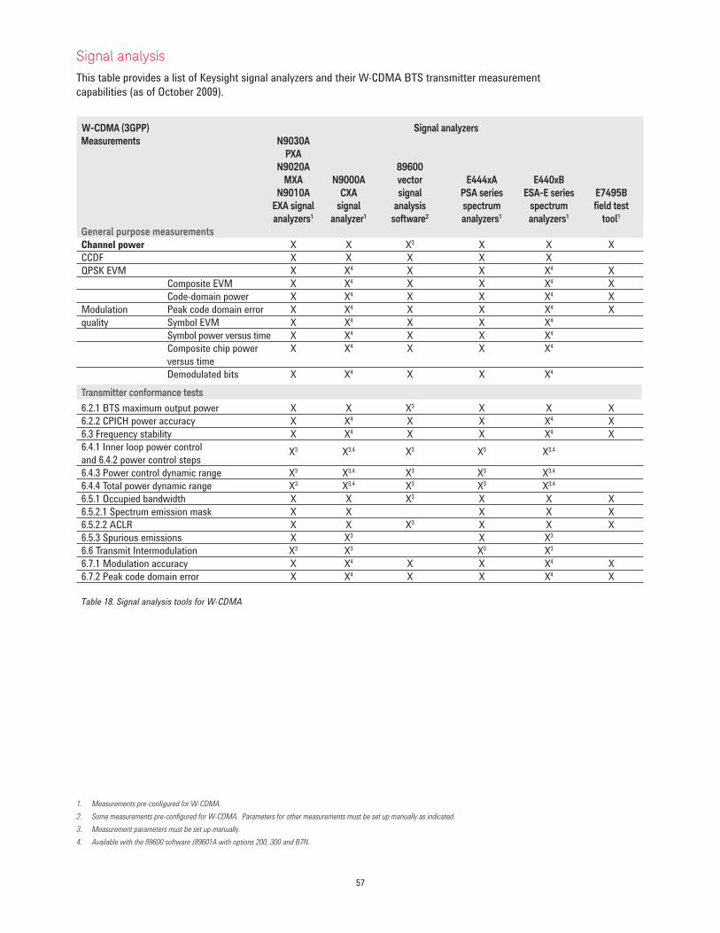
Signal analysisThis table provides a list of Keysight signal analyzers and their W-CDMA BTS transmitter measurement capabilities (as of October 2009) .
W-CDMA (3GPP) Signal analyzers Measurements N9030A PXA N9020A 89600 MXA N9000A vector E444xA E440xB N9010A CXA signal PSA series ESA-E series E7495B EXA signal signal analysis spectrum spectrum field test analyzers1 analyzer1 software2 analyzers1 analyzers1 tool1
General purpose measurements Channel power X X X3 X X XCCDF X X X X XQPSK EVM X X4 X X X4 X Composite EVM X X4 X X X4 X Code-domain power X X4 X X X4 XModulation Peak code domain error X X4 X X X4 Xquality Symbol EVM X X4 X X X4
Symbol power versus time X X4 X X X4
Composite chip power X X4 X X X4
versus time Demodulated bits X X4 X X X4
Transmitter conformance tests6 .2 .1 BTS maximum output power X X X3 X X X6 .2 .2 CPICH power accuracy X X4 X X X4 X6 .3 Frequency stability X X4 X X X4 X6 .4 .1 Inner loop power control X3 X3,4 X3 X3 X3,4
and 6 .4 .2 power control steps6 .4 .3 Power control dynamic range X3 X3,4 X3 X3 X3,4
6 .4 .4 Total power dynamic range X3 X3,4 X3 X3 X3,4
6 .5 .1 Occupied bandwidth X X X3 X X X6 .5 .2 .1 Spectrum emission mask X X X X X6 .5 .2 .2 ACLR X X X3 X X X6 .5 .3 Spurious emissions X X3 X X3
6 .6 Transmit Intermodulation X3 X3 X3 X3
6 .7 .1 Modulation accuracy X X4 X X X4 X 6 .7 .2 Peak code domain error X X4 X X X4 X Table 18. Signal analysis tools for W-CDMA
1. Measurements pre-configured for W-CDMA. 2. Some measurements pre-configured for W-CDMA. Parameters for other measurements must be set up manually as indicated. 3. Measurement parameters must be set up manually. 4. Available with the 89600 software (89601A with options 200, 300 and B7N.
57
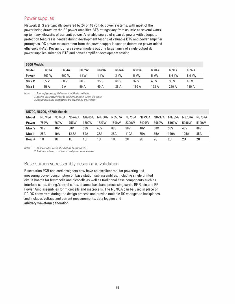
Power suppliesNetwork BTS are typically powered by 24 or 48 volt dc power systems, with most of the power being drawn by the RF power amplifier . BTS ratings vary from as little as several watts up to many kilowatts of transmit power . A reliable source of clean dc power with adequate protection features is needed during development testing of valuable BTS and power amplifier prototypes . DC power measurement from the power supply is used to determine power-added efficiency (PAE) . Keysight offers several models out of a large family of single output dc power supplies suited for BTS and power amplifier development testing .
Notes: 1. Autoranging topology. Full power from 20 volts to 60 volts. 2. Identical power supplies can be paralleled for higher current and power. 3. Additional volt/amp combinations and power levels are available.
Base station subassembly design and validation Basestation PCB and card designers now have an excellent tool for powering and measuring power consumption on base station sub assemblies, including single printed circuit boards for femtocells and picocells as well as traditional base components such as interface cards, timing/control cards, channel baseband processing cards, RF Radio and RF Power Amp assemblies for microcells and macrocells . The N6705A can be used in place of DC-DC converters during the design process and provide multiple DC voltages to backplanes, and includes voltage and current measurements, data logging and arbitrary waveform generation .
N5700, N6700, N8700 Models
Model N5745A N5746A N5747A N6765A N6766A N6567A N8735A N8736A N8737A N8755A N8756A N8757APower 750W 760W 750W 1500W 1520W 1500W 3300W 3400W 3000W 5100W 5000W 5100WMax V 30V 40V 60V 30V 40V 60V 30V 40V 60V 30V 40V 60VMax I 25A 19A 12 .5A 50A 38A 25A 110A 85A 55A 170A 125A 85AHeight 1U 1U 1U 1U 1U 1U 2U 2U 2U 2U 2U 2U
6600 Models
Model 6653A 6654A 6032A1 6673A 6674A 6683A 6684A 6691A 6692APower 500 W 500 W 1 kW 1 kW 2 kW 5 kW 5 kW 6 .6 kW 6 .6 kWMax V 35 V 60 V 60 V 35 V 60 V 32 V 40 V 30 V 60 VMax I 15 A 9 A 50 A 60 A 35 A 160 A 128 A 220 A 110 A
Notes: 1. All new models include USB/LAN/GPIB connectivity. 2. Additional volt/amp combinations and power levels available.
58

Considerations for femtocell design and test
Design and development
Femtocell design and development will mainly use the same measurement tools and techniques as for standard classes of base stations, with the addition of UE receiver test to verify the performance of the sniffer function required for auto-setup . In addition, integration of GPS functionality must be verified where required .
The simplified UE receiver used as the sniffer must be able to identify the parameters of all active cells in the area – both other network cells and other femtocells – so that the femtocell setup does not cause interference . Testing the receiver will include only basic functions – sensitivity, frequency and power measurements, demodulation, and the identification of the scrambling codes being used . Design verfification will also check interference characteristics such as spurious conducted and radiated emmissions .
Manufacturing testThe volume and cost envelope of the femtocell product needs special attention in manufacturing . As described earlier, it is subject to 3GPP standards definitions and spec-ifications in the same way as other network equipment, so a manufacturing regime that does enough testing to ensure compliance, while at the same time minimizing test time and cost, must be defined .
A typical manufacturing process flow is shown in Figure 41 . This type of process essen-tially relies on full testing of some percentage of the product to give confidence that the process is stable and working correctly, and if the sample fails the entire output will be sent for rework . Most tests will be limited to a subset of possible bands and channel bandwidths where device performance is statistically weakest, which will be determined from data gathered in sample testing .
In early production, a large sample size – up to 100% in pilot production – will be used, with the percentage dropping as confidence in the product and test regime grows, to perhaps 1 in 100 for medium volume mature production and to 1 in 1000 for high volumes .
Figure 41. Typical high-volume manufacturing process flow
59
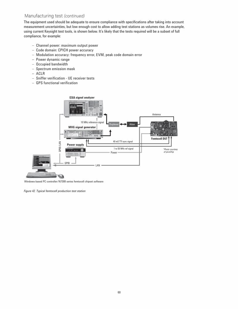
10 MHz reference signal
Windows-based PC controller/N7300 series femtocell chipset software
EXA
*Photo courtesy of picoChip
The equipment used should be adequate to ensure compliance with specifications after taking into account measurement uncertainties, but low enough cost to allow adding test stations as volumes rise . An example, using current Keysight test tools, is shown below . It’s likely that the tests required will be a subset of full compliance, for example:
– Channel power: maximum output power – Code domain: CPICH power accuracy – Modulation accuracy: frequency error, EVM, peak code domain error – Power dynamic range – Occupied bandwidth – Spectrum emission mask – ACLR – Sniffer verification - UE receiver tests – GPS functional verification
–
Figure 42. Typical femtocell production test station
Manufacturing test (continued)
60
Instruments used for measurement examples
Additional information can be found on Keysight's product web sites: www.keysight.com/find/ESGwww.keysight.com/find/PSAwww.keysight.com/find/PXAwww.keysight.com/find/PXBwww.keysight.com/find/MXAwww.keysight.com/find/MXGwww.keysight.com/find/89601A www.keysight.com/find/signalstudiowww.keysight.com/find/EXAwww.keysight.com/find/n7300
Figure 43. The measurement examples and screen images in this application note were obtained using the following instruments
The following instruments can also be used to make the same measurements:
PSA series spectrum analyzer or E4406A VSA transmitter
N9020A MXA signal analyzer
N5106A PXB baseband generator and channel emulator
N9030A PXA signal analyzer
N9010A EXA signal analyzer
Signal Studio SoftwareN7300 series femtocell chipset software
E4438C ESG vector signal generator
N9030A PXA signal analyzer
89601A Vector Signal Analysis Software
61

Acronym Glossary 2G Second Generation3G Third Generation3GPP Third-Generation Partnership Project ACIR Adjacent Channel Interference RatioACL Adjacent Channel LeakageACLR Adjacent Channel Leakage Power RatioACPR Adjacent Channel Power RatioACS Adjacent Channel Selectivity AICH Acquisition Indication ChannelARIB Association of Radio Industries and Businesses (Japan)AWGN Additive White Gaussian NoiseBCH Broadcast ChannelBCCH Broadcast Control ChannelBER Bit Error RateBLER Block Error Rate BPSK Binary Phase Shift KeyingBTFD Blind Transport Format DetectionBTS Base Transceiver StationCCCH Common Control ChannelCCDF Complementary Cumulative Distribution FunctionCCTrCH Coded Composite Transport ChannelCDF Cumulative Density FunctionCDMA Code Division Multiple AccesscdmaOne Name identifying the EIA/TIA standard (commonly referred to as IS-95) for 2Gcdma2000 Name identifying the EIA/TIA standard (IS-2000) for 3GCFN Connection frame number C/N Carrier-to-Noise RatioCPCH Common Packet ChannelCPICH Common Pilot ChannelCQI Channel Quality IndicatorCRC Cyclic Redundancy CheckCW Continuous Wave (unmodulated signal)DCH Dedicated ChannelDCCH Dedicated Control Channel DL DownlinkDPCCH Dedicated Physical Control ChannelDPDCH Dedicated Physical Data ChannelDQPSK Differential Quadrature Phase Shift Keying DSP Digital Signal ProcessingDTCH Dedicated Traffic ChannelDTX Discontinuous TransmissionEb/No Energy-per-Bit-to-Noise RatioEc/No Energy-per-Chip-to-Noise Ratio E-DCH Enhanced Dedicated ChannelE-DPCCH Enhanced Dedicated Physical Control ChannelE-DPDCH Enhanced Dedicated Physical Data ChannelETSI European Telecommunications Standard Institute EVM Error Vector MagnitudeFACH Forward Access ChannelFBI Feedback InformationFDD Frequency Division DuplexFER Frame Error RatioFRC Fixed Reference ChannelGMSK Gaussian Minimum Shift KeyingGPS Global Positioning SystemGSM Global System for Mobile Communications HARQ Hybrid Automatic Repeat RequestHPSK Hybrid Phase Shift KeyingHSDPA High Speed Downlink Packet AccessHS-DPCCH High Speed Dedicated Physical Control ChannelHS-DSCH High Speed Downlink Shared ChannelHSPA High Speed Packet AccessHS-PDSCH High Speed Physical Downlink Shared ChannelHS-SCCH High Speed Shared Control Channel for HS-DSCHHSUPA High Speed Uplink Packet AccessIF Intermediate FrequencyIMT-2000 International Mobile Telecommunications-2000 (Collective name for 3G technologies approved by the ITU)
I/Q In-phase/QuadratureIS-2000 EIA/TIA interim standard 2000 (see cdma 2000)IS-95 Interim Standard for U .S . Code Division Multiple AccessLO Local OscillatorMAC Medium Access ControlMIMO Multiple Input Multiple OutputMISO Multiple Input Single OutputOCNS Orthogonal Channel Noise SimulatorOCQPSK Orthogonal Complex Quadrature Phase Shift KeyingOSI Open System InterconnectionOVSF Orthogonal Variable Spreading FactorPA Power AmplifierPAE Power-Added EfficiencyPAR Peak-to-Average Power RatioPCH Paging ChannelPCCH Paging Control ChannelP-CCPCH Primary Common Control Physical ChannelPCPCH Physical Common Packet ChannelPDC Pacific Digital Cellular System PDF Probability Density FunctionPDSCH Physical Downlink Shared Channel PICH Paging Indication ChannelPN Pseudo-NoisePRACH Physical Random Access ChannelPSC Primary Synchronization CodeP-SCH Primary Synchronization ChannelPSK Phase Shift KeyingQAM Quadrature Amplitude ModulationQPSK Quadrature Phase Shift KeyingRACH Random Access ChannelR&D Research and DevelopmentRF Radio FrequencyRLC Radio Link ControlRMC Reference Measurement ChannelRMS Root Mean SquareRRC Root Raised CosineRRC Radio Resource Control S-CCPCH Secondary Common Control Physical ChannelSCH Synchronization ChannelSF Spreading FactorSFN System Frame NumberSIMO Single Input Multiple OutputSIR Signal to Interference RatioSISO Single Input Single OutputSSC Secondary Synchronization CodeS-SCH Secondary Synchronization ChannelTDD Time Division DuplexTDMA Time Division Multiple AccessTF Transport FormatTFC Transport Format CombinationTFCI Transport Format Control IndicatorTFCS Transport Format Combination SetTGPRC Transmission Gap Pattern Repetition Count TGCFN Transmission Gap Connection Frame Number TGSN Transmission Gap Slot Number TGL1 Transmission Gap Length 1 TGL2 Transmission Gap Length 2 TGD Transmission Gap Duration TGPL1 Transmission Gap Pattern Length 1 TGPL2 Transmission Gap Pattern Length 2 TGPSI Transmission Gap Pattern Sequence Identifier TIA Telecommunications Industries Association (U .S .)TPC Transmit Power ControlTTA Telecommunications Technology Association (Korea) TTC Telecommunication Technology Committee (Japan)TTI Transmission Time IntervalUE User EquipmentUL UplinkUMTS Universal Mobile Telephone System (Europe)W-CDMA Wideband-Code Division Multiple Access (3G system)
62

References
3rd Generation Partnership Project, Technical Specification Group Radio Access Network, Releases 99 through 8: Base Station Conformance Specification . Radio Transmission and Reception (FDD) . TS 25 .141 . Multiplexing and Channel Coding (FDD) . TS 25 .212 . Medium Access Control Protocol Specification . TS 25 .321 . Radio Link Control Protocol Specification . TS 25 .322 . Radio Resource Control Protocol Specification . TS 25 .331 . Radio Interface Protocol Architecture . TS 25 .301 . Physical Layer: Physical Channels and Mapping of Transport Channels onto Physical Channels (FDD) . TS 25 .211 Physical Layer: Spreading and Modulation (FDD) . TS 25 .213 . Physical Layer: Channel Coding and Multiplexing Examples . TS 25 .944 . BS Radio Transmission and Reception (FDD) . TS 25 .104 UTRAN Overall Description . TS 25 .401
3rd Generation Partnership Project . Technical Specification Group Terminal; Terminal Conformance Specification . Radio Transmission and Reception (FDD) . Release 99 . TS 34 .121
Keysight Technologies references:
HPSK Spreading for 3G, Application Note 1335, literature number 5968-8438E .
Fundamentals of RF and Microwave Power Measurements, Application Note 64-1C, literature number 5965-6630E .
Characterizing Digitally Modulated Signals with CCDF Curves, Application Note, literature number 5968-6875E .
Testing and Troubleshooting Digital RF Communications Transmitter Designs, Application Note 1313, literature number 5968-3578E .
Testing and Troubleshooting Digital RF Communications Receiver Designs, Application Note 1314, literature number 5968-3579E .
Related Keysight Literature
3GPP W-CDMA Design Library, literature number 5980-0953E .
MXA Signal Analyzers Brochure, literature number 5989-5047EN .
EXA Signal Analyzer Brochure, literature number 5989-6527EN .
MXG Signal Generators Brochure, literature number 5989-5074EN .
PXA High Performance Signal Analyzer Brochure, literature number 5990-3951EN .
PXB Baseband Generator and Channel Emulator Brochure, literature number 5989-8970EN .
PSA Series Performance Spectrum Analyzers Brochure, literature number 5980-1283E .
ESA-E Series Spectrum Analyzers Brochure, literature number 5968-3278E .
ESA Instrument Connected Solutions Configuration Guide, literature number 5988-6561EN .
EPM Series Power Meters Brochure, literature number 5965-6380E .
EPM-P Series Single – and Dual – Channel Power Meters/ E9320 Family of Peak and Average Power Sensors Product Overview, literature number 5980-1471E .
89600 Series Wide Bandwidth Vector Signal Analyzers, literature number 5980-0723E .
E4438C ESG Vector Signal Generator Brochure, literature number 5988-3935EN .
Family of DC Power Supplies Brochure, literature number 5988-2384EN .
E7495B Base Station Test Set Technical Overview, literature number 5988-7186EN .
63
Web Resources
For additonal product information and literature, visit our Web sites:
www.keysight.com/find/ESGwww.keysight.com/find/PSA www.keysight.com/find/PXA www.keysight.com/find/PXB www.keysight.com/find/MXA www.keysight.com/find/MXG www.keysight.com/find/89601A www.keysight.com/find/signalstudio

64 | Keysight | Designing and Testing 3GPP W-CDMA Base Transceiver Stations (including Femtocells) – Application Note
This information is subject to change without notice.© Keysight Technologies, 2003 - 2010, 2014Published in USA, July 31, 20145980-1239Ewww.keysight.com
For more information on Keysight Technologies’ products, applications or services, please contact your local Keysight office. The complete list is available at:www.keysight.com/find/contactus
Americas Canada (877) 894 4414Brazil 55 11 3351 7010Mexico 001 800 254 2440United States (800) 829 4444
Asia PacificAustralia 1 800 629 485China 800 810 0189Hong Kong 800 938 693India 1 800 112 929Japan 0120 (421) 345Korea 080 769 0800Malaysia 1 800 888 848Singapore 1 800 375 8100Taiwan 0800 047 866Other AP Countries (65) 6375 8100
Europe & Middle EastAustria 0800 001122Belgium 0800 58580Finland 0800 523252France 0805 980333Germany 0800 6270999Ireland 1800 832700Israel 1 809 343051Italy 800 599100Luxembourg +32 800 58580Netherlands 0800 0233200Russia 8800 5009286Spain 800 000154Sweden 0200 882255Switzerland 0800 805353
Opt. 1 (DE)Opt. 2 (FR)Opt. 3 (IT)
United Kingdom 0800 0260637
For other unlisted countries:www.keysight.com/find/contactus(BP-09-23-14)
myKeysight
www.keysight.com/find/mykeysightA personalized view into the information most relevant to you.
www.lxistandard.org
LAN eXtensions for Instruments puts the power of Ethernet and the Web inside your test systems. Keysight is a founding member of the LXI consortium.
Three-Year Warranty
www.keysight.com/find/ThreeYearWarrantyKeysight’s commitment to superior product quality and lower total cost of ownership. The only test and measurement company with three-year warranty standard on all instruments, worldwide.
Keysight Assurance Planswww.keysight.com/find/AssurancePlansUp to five years of protection and no budgetary surprises to ensure your instruments are operating to specification so you can rely on accurate measurements.
www.keysight.com/go/qualityKeysight Technologies, Inc.DEKRA Certified ISO 9001:2008 Quality Management System
Keysight Channel Partnerswww.keysight.com/find/channelpartnersGet the best of both worlds: Keysight’s measurement expertise and product breadth, combined with channel partner convenience.
This document was formerly known as application note 1355. www.keysight.com/find/wcdma