Measurements on 3GPP Base Station Transmitter Signals · PDF fileMeasurements on 3GPP Base...
26
Subject to change – Josef Wolf 08/01 - 1EF44_1E Products: Signal Analyzer FSIQ (with option FSIQ-B70 and FSIQ-K72) Measurements on 3GPP Base Station Transmitter Signals This application note explains the measurements on 3GPP Base Station Transmitter signals according to TS 25.141, using the Signal Analyzer FSIQ with the Code Domain Power application firmware FSIQ-K72.
Transcript of Measurements on 3GPP Base Station Transmitter Signals · PDF fileMeasurements on 3GPP Base...
Subject to change – Josef Wolf 08/01 - 1EF44_1E
Products: Signal Analyzer FSIQ (with option FSIQ-B70 and FSIQ-K72)
Measurements on3GPP Base Station Transmitter Signals
This application note explains the measurements on 3GPP Base Station Transmitter signals according toTS 25.141, using the Signal Analyzer FSIQ with the Code Domain Power application firmware FSIQ-K72.
3GPP Base Station Transmitter Test
1EF44_1E 2 Rohde & Schwarz
Contents
1 Overview ............................................................................................. 3
2 Structure of the 3GPP W-CDMA Signal ............................................... 3Structure in Code Domain............................................................... 3Structure in Time Domain ............................................................... 4
Dedicated Physical Channel (DPCH) ......................................... 5Common Pilot Channel (CPICH)................................................ 5Paging Indication Channel (PICH).............................................. 6Synchronization Channel (SCH)................................................. 6Primary Common Control Physical Channel (P-CCPCH) ........... 6Secondary Common Control Physical Channel (S-CCPCH) ....... 7PCH - Paging Channel ............................................................... 7FACH - Forward Access Channel............................................... 8Code Channel Timing Offsets .................................................... 8
3 Measurements in Code Domain........................................................... 9Test Models .................................................................................... 9
Maximum Output Power ............................................................ 9CPICH Power Accuracy ........................................................... 11Frequency Stability .................................................................. 11Power Control Steps and Combined Power Control Tolerance . 12Total Power Dynamic Range.................................................... 13Power Control Dynamic Range ................................................ 13Measurement of the Transmit Modulation Quality .................... 14Modulation Accuracy (EVM)..................................................... 14Peak Code Domain Error (PCDE) ............................................ 16
4 Measurements in Spectrum Domain .................................................. 18Occupied Bandwidth (OBW) .................................................... 18Spectrum Emission Mask......................................................... 18Measurement of the Adjacent Channel Leakage Ratio (ACLR). 20
5 Additional Useful Code Domain Measurements ................................. 22
6 Additional Useful Spectrum Measurements........................................ 24
7 Test Tolerances................................................................................. 25
8 Abbreviations..................................................................................... 25
9 Literature ........................................................................................... 26
10 Ordering information.......................................................................... 26
3GPP Base Station Transmitter Test
1EF44_1E 3 Rohde & Schwarz
1 Overview
With the introduction of a CDMA transmission scheme for the third generationof mobile radio systems new requirements on test equipment arise. The CDMAtransmission scheme is already in use and the measurement techniques arewell known from the existing IS 95 system. However, due to the variable andhigher data rates possible with the W-CDMA system currently specified within3GPP, the signal structure is more complex compared to IS 95. With the3GPP system each user can be assigned a different bit rate from 7.5 kbit/s to 2Mbit/s. This is not the case with the second generation systems.
The conformance test for W-CDMA base station transmitters is describedin the 3GPP document TS 25.141. It requires different measurements onBase Station (BS) transmit signals that are only possible to perform by de-spreading the CDMA signal into the different code channels. A dedicatedanalyzer is necessary to de-spread the signal and measure power of thedifferent code channels, as well as the modulation quality of the wholesignal. In addition to these in-band measurements, out of bandtransmission and spurious measurements are necessary to ensureprotection of other W-CDMA channels or other radio systems frominterference. Additional measurements not required by the standard aredesirable, for example to assure on module level that the whole basestation transmitter will work or to troubleshoot non-working modules.
The structure of the W-CDMA signal is explained as far as this knowledgeis needed for understanding the measurement. Especially with the in-channel measurement explained in section 3 and 5 the structure of thesignal is of importance. In section 4 the out-of-band measurements arediscussed. These are spectrum measurements requiring specific functionsof the spectrum analyzer.
In chapter 7 the difference between the minimum requirements and thetest requirements and their relation to the test tolerances is described. Therequirement values used in this document are the test requirements.
2 Structure of the 3GPP W-CDMA Signal
To help understand the measurements in the code domain this sectiongives a short overview of the W-CDMA Down Link (DL) signal structure.
Structure in Code Domain
Different bit rates for data transmission are implemented in the 3GPPstandard by using different spreading factors of the information bits.Spreading Factors (SF) between 4 and 512 are defined. Each SF isassigned a number of code channels. The number of code channelsavailable for a specific SF is dependent on the SF itself. The different codechannels can be shown in the so-called code tree (see figure 1).
The different codes with a specific SF are orthogonal (vertical bars in fig 1).The codes of branches in the tree (connected through lines in figure 1) arerelated to each other, i. e. they are not orthogonal. If one single code channel ina branch of the code tree is occupied, other users cannot use all other codes inthe branch.

3GPP Base Station Transmitter Test
1EF44_1E 4 Rohde & Schwarz
With a spreading factor of 4 four users are possible in theory. With aspreading factor of 512 the theoretical maximum number of users is 512.However, not all channels can be used for payload. Some channels mustbe used for network signaling overhead, such as exchanging networkinformation with the users or for initiating a call. For the purposes of thisapplication note, these network signaling channels are referred to asorganization channels. The most important organization channels are:
CPICH Common Pilot Channel (SF 256, position 0)
PICH Paging indication channel (SF 256, position 16)
PCCPCH Primary common control physical channel(SF 256, position 1)
SCCPCH Secondary Common Control Physical Channel
PSCH Primary Synchronization channel
SSCH Secondary Synchronization Channel
The PSCH and the SSCH are only transmitted during the first 256 chips ofa slot. They are not orthogonal because they are superimposed on theother channels. Therefore they are not assigned to a code position.
C0
C2,0
C2,1
C4,0
C4,1
C4,2
C4,3
C8,0
C8,1
C8,2
C8,3
C8,4
C8,5
C8,6
C8,7
SF2 SF4 SF8 SF16SF0 SF512SF256CPICH
PCCPCH
PICH
0
1
16
Fig 1 Code Tree of a W-CDMA signal. The organization channels areshown on their position in code class 256 (15 kbps)
Structure in Time Domain
The W-CDMA signal is organized in frames with a length of 10 ms. Aframe consists of 15 slots. With the 3.84 MHz chip rate used each slotcontains 2560 chips.
The structure and the purpose of the different channels are explainedbelow with respect to their use for transmitter measurements.

3GPP Base Station Transmitter Test
1EF44_1E 5 Rohde & Schwarz
Dedicated Physical Channel (DPCH)
A traffic channel for transmission of voice or user data in downlink has thestructure shown in figure 2.
One radio frame, Tf = 10 ms
TPC NTPC bits
Slot 0 Slot 1 Slot i Slot 14
Tslot = 2560 chips, 10*2k bits (k=0..7)
Data2Ndata2 bits
DPDCH
TFCI NTFCI bits
Pilot Npilot bits
Data1Ndata1 bits
DPDCH DPCCH DPCCH
Fig 2 Structure of a W-CDMA traffic channel in time domain
DPCCH = Dedicated Physical Control Channel
DPDCH = Dedicated Physical Data Channel
TFCI = Transport Format Combination Indicator
TPC = Transmit Power Control
Pilot = Pilot Symbols
The DPCH contains control and data information. The data portioncontains the Dedicated Physical Data Channel (DPDCH), with 4 to 1248data bits, dependent on the spreading factor of the code channel. Controlinformation includes
• the DPCCH (Dedicated Physical Control Channel) comprising the Pilotsymbols,
• the Transmit Power Control (TPC) bits and
• the Transport Format Combination Indicator (TFCI) bits.
The number of pilot bits can vary between 2 and 16. The number of TPCbits is 2, 4 or 8. For higher bit rates more TPC bits are used. An all zeroTPC bit pattern stands for a power down command for the mobile stationand an all one bit pattern for a power up command for the mobile station.
Common Pilot Channel (CPICH)
To synchronize the mobile station the base station transmits a Common PilotChannel (CPICH) with a pre-defined symbol sequence. It is transmittedcontinuously at a fixed power level. Its structure is shown in figure 3.
Predefined Symbol Sequence
Slot 0 Slot 1 Slot i Slot 14
2560 chips, 20 bits / 10 symbols
Tf = 10 ms
Fig 3 Structure of the Common Pilot Channel (CPICH)

3GPP Base Station Transmitter Test
1EF44_1E 6 Rohde & Schwarz
The spreading factor of the CPICH is 256; i. e. the transmission rate is 30kbps. In the code tree the CPICH is on position 0. By default the CPICH isthe phase reference for all other channels in the downlink.
Paging Indication Channel (PICH)
288 bits for paging indication 12 bits (unused)
One frame (10 ms)
Fig 4 Structure of the Paging Indication Channel (PICH)
The PICH does not contain any pilot or other control channels. If thePaging Indicator in a certain frame is set to "1" it is an indication for mobilestations associated with this page indicator to read a message in thecorresponding frame of the associated Secondary Common ControlPhysical Channel (S-CCPCH).
Synchronization Channel (SCH)
The Synchronization Channel (SCH) is for cell search. It consists of twosub-channels, the Primary SCH (P-SCH) and Secondary SCH (S-SCH).The 10 ms frames of the Primary and Secondary SCH are divided into 15slots, each of length 2560 chips. Figure 5 illustrates the structure of theSCH radio frame.
cp : Primary Synchronization Code
cs
i,
k : One of 16 possible Secondary Synchronization Codes
cp
csi,1
cp cp
T slot = 2560 chips
Tframe = 15*Tslot
PrimarySCHSecondarySCH
256 chips
csi,2 cs
i,16
(csi,1,cs
i,2, ..., csi,15) encode cell specific long scrambling code group i
Slot 0 Slot 1 Slot 14
Fig 5 Structure of the Synchronization Channel (SCH)
The synchronization channel is non-orthogonal to the other channels and isonly switched on during the first 256 chips of each slot.
The P-SCH is the same in all slots of the frame, where as the S-SCHchanges every slot. This enables the mobile to reasonably quickly searchfor the P-SCH to establish the frame timing, and then use the S-SCH tofind the slot timing. The sequence on the Secondary SCH also indicateswhich scrambling code is used in the cell.
As the SCH is non orthogonal it creates some interference in all otherchannels. EVM measurement in the presence of the SCH requires specialtechniques in the test equipment to remove the effects of this distortion.
Primary Common Control Physical Channel (P-CCPCH)
The P-CCPCH is a fixed rate (30 kbps, SF = 256) downlink physicalchannel used to carry the Broadcast Channel (BCH). The BCH sendssystem- and cell-specific information to all users. It is always transmittedover the entire cell with a low fixed bit rate.

3GPP Base Station Transmitter Test
1EF44_1E 7 Rohde & Schwarz
Figure 6 shows the frame structure of the P-CCPCH. The frame structurediffers from the downlink DPCH in that no TPC commands, no TFCI andno pilot bits are transmitted The P-CCPCH is not transmitted during thefirst 256 chips of each slot. Instead, Primary SCH and Secondary SCH aretransmitted during this period (see figure 5).
Data 18 bits
Slot 0 Slot 2 Slot i Slot 14
2560 chips, 10 symbols (20 bits)
TXoff
TFrame = 10 ms
256 chips 2304 chips
Fig 6 Structure of the Primary Common Control Physical Channel(P-CCPCH)
Secondary Common Control Physical Channel (S-CCPCH)
The S-CCPCH is used to carry the Forward Access Channel (FACH) andthe Paging Channel (PCH). FACH and PCH are used to send shortmessages to the mobile, the User Equipment (UE). The S-CCPCH can usethe same set of spreading factors as the downlink DPCH. The framestructure of the Secondary CCPCH is shown in figure 7
Slot 0 Slot 1 Slot i Slot 14
Tslot = 2560 chips, 20*2k bits (k=0..6)
Pilot Npilot bits
DataNdata bits
1 radio frame: Tf = 10 ms
TFCI NTFCI bits
Fig 7 Structure for Secondary Common Control Physical Channel(S-CCPCH)
The parameter k in figure 7 determines the total number of bits perdownlink Secondary CCPCH slot. It is related to the spreading factor SF ofthe physical channel as SF = 256/2k. The spreading factor range is from256 down to 4.
The main difference between the Primary and Secondary CCPCH is thatthe transport channel mapped to the Primary CCPCH (BCH) can only havea fixed data rate, while the Secondary CCPCH supports multiple datarates.
PCH - Paging Channel
The PCH is a downlink channel used to broadcast control information intoan entire cell, allowing the UE efficient sleep mode procedures.

3GPP Base Station Transmitter Test
1EF44_1E 8 Rohde & Schwarz
FACH - Forward Access Channel
The FACH is a downlink transport channel used to transmit shortmessages to the UE. The FACH is transmitted over the entire cell or overonly a part of the cell. The FACH can be transmitted using slow powercontrol.
Code Channel Timing Offsets
The power of each user code channel is controlled on slot basis.Dependent on the transmission quality the mobile station reports, the basestation adjusts the power of each individual code channel separately.
To minimize the crest factor of the W-CDMA signal, each code channelcan be assigned a timing offset such that the absolute time of a slot isdifferent for each channel. The reference channel is the CPICH. Thetiming offset can be between 0 and 38144 chips in steps of 256 chips, ornearly a complete frame.
PCCPCH + SCH
FrameCPICH0
Timing offset = 2
��
PICH
DPCH1 (SF =128, Code No = 24)
DPCH2 (SF = 128, Code No = 72)
DPCH3 (SF = 128, Code No = 120)
0
0
0
0
��
��
��
��
0
1 �� ��
Slot
t=0
Timing offset = 7
Timing offset =120
Timing offset = 1
Timing offset = 0
Timing offset = Reference
t = 10 ms
Fig 8 Absolute timing of the code channels of test model 1.
During a CPICH timeslot, the other active channels may belong to adifferent slot number or even to a different frame number compared to theCPICH. Due to the timing offset two different time scalings can be defined:
• With absolute time scaling the power of all code channels is referencedto the CPICH. With this absolute time reference the slot timing of allother channels do not necessarily match the slot timing of the CPICH.
• With logical time scaling all channels are regarded in respect to theirframe number and timeslot number. The logical time scalingcorresponds to the absolute time scaling, if the timing offsets areremoved and the corresponding timeslots are overlaid.
The FSIQ uses absolute time scaling referenced to the start of CPICH slot0 for measurements in the code domain. The power in the different codechannels is displayed in the raster of the CPICH timeslots.

3GPP Base Station Transmitter Test
1EF44_1E 9 Rohde & Schwarz
3 Measurements in Code Domain
The most prominent requirement for in-channel measurements on W-CDMA signals is Code Domain Power analysis. As all channels use thesame spectrum, the measurement must be performed by de-spreading theW-CDMA signal into its individual code channels and measuring theirindividual power and quality.
Test Models
The 3GPP standard TS 25.141 defines four different test models to assurethat the results between different base stations are comparable.
Each of these test models contain organization channels listed on page 4 and anumber of Dedicated Physical Channels, each using the spreading factor 128or 256 (corresponds to 30 kbps or 15 kbps transmission rate). Each channel isassigned a specific power level and timing offset. The contents of the differentchannels of the test models are exactly specified in TS 25.141.
Test model 1 is primarily used for measurement of the out of bandspectrum and the maximum output power of the base station. It uses 64user code channels at 30 kbps (spreading factor 128) randomly distributedacross the code space with random power levels and random timingoffsets. The intention is to use a signal with a high crest factor to simulatea realistic traffic scenario. If the base station does not support 64 trafficchannels, models using 32 or 16 traffic channels are specified.
Test model 1 is used with the following measurements specified in TS 25.141:
• spectrum emission mask
• adjacent channel leakage ratio (ACLR)
• spurious emissions
• transmit intermodulation
• base station maximum output power
Test model 2 is used for the measurement of the output power dynamicswith the exception of total power dynamic range. It comprises theorganization channels P-CCPCH + SCH, CPICH, PICH, S-CCPCHcontaining PCH and 3 traffic channels, each with 30 kbps transmissionrate.
Test model 3 is used for the measurement of Peak Code Domain Error(PCDE). It contains in addition to the organization channels P-CCPCH + SCH,CPICH, PICH, S-CCPCH containing PCH, and 16 or 32 traffic channels eachwith spreading factor 256 (= 15 kbps transmission rate), dependent on thecapability of the base station.
Test model 4 is used for measurement of Error Vector Magnitude (EVM) andtotal power dynamic range. It uses the P-CCPCH, SCH and CPICH (optional),only. No traffic channel is active.
Maximum Output Power
For the measurement of the maximum output power test model 1 is used.
Maximum output power of the base station is the mean power level percarrier at the antenna connector as specified by the manufacturer. It isdefined as the mean power over certain slots and shall be within 2.7 dB ofthe manufacturer’s specification.

3GPP Base Station Transmitter Test
1EF44_1E 10 Rohde & Schwarz
Measurement of the mean power can be performed in two different ways:
• The FSIQ uses the integrated bandwidth method in spectrum mode tomeasure the channel power. Using the rms detector the measurementresult is very accurate and repeatable. However, there is no relation tospecific slots of the W-CDMA signal.
• Using the Code domain power function of the option FSIQ-K72, the poweris measured during a selectable slot of the W-CDMA signal. To enable theFSIQ to detect the PICH in test model 1, it supports the selection of thetest model to be measured. With the test model selected, the FSIQ knowsthe code configuration of the test signal in advance. The calculations incode domain are then performed exactly to the specification. The testresult is reported as a numeric value in the result summary.
Ref Lvl9 dBmRef Lvl9 dBmRef Lvl9 dBmRef Lvl9 dBm
dB
Ref Lvl9 dBmRef Lvl9 dBmRef Lvl9 dBmRef Lvl9 dBm
-28
-21
A
B
START: CH 0 STOP: CH 51164 CH/DIV
CF 2.1175 GHzCode Pwr RelativeCode Pwr RelativeCPICH Slot 0CPICH Slot 0
SR 30 kspsChan Code 62Chan Code 62Chan Slot 0Chan Slot 0
CF 2.1175 GHzResult SummaryResult SummaryCPICH Slot 0CPICH Slot 0
SR 30 kspsChan Code 62Chan Code 62Chan Slot 0Chan Slot 0
-63
-56
-49
-42
-35
-28
-21
-7
-70
0
��
Chip Rate Err -0.04 ppm �IQ Offset 0.26 % �Modulation Acc 2.66 % rms �CPICH Slot Number 0 �
©©©©©©©©©©©©©©©©©©©©©©©©©©©©©©©©©©ª©©©©©©©©©©©©©©©©©©©©©©©©©©©©©©©©©©CHANNEL RESULTS �
Symb Rate 30 ksps � Timing Offset 256 ChipsChannel Code 62 � Chan Slot Number 0Chan Pow rel. -6.01 dB � Chan Pow abs. -15.94 dBmError Vector Mag 1.26 % rms � Error Vector Mag 2.37 % Pk
Total PWR 0.07 dBmGLOBAL RESULTS
RESULT SUMMARY
Carr Freq Err 81.07 HzTrg to Frame 3.15 msIQ Imbalance 0.55 %Pk Code Dom Err -52.21 dB rms
( 15 ksps)
Fig 9 Numeric measurement result for the total power using test model 1(Total Pwr, arrowed)
In addition to the total power the result summary table shows other usefulinformation characterizing the W-CDMA signal in more detail. Some of themeasurement values apply to the whole signal such as the carrier frequencyerror, chip rate error, modulation accuracy (EVM) and the peak code domainerror (PCDE). They are listed in the section GLOBAL RESULTS. In addition tothe Global Results, characteristics and test results for a specific code channelare output. These are the symbol rate, the code number, the slot number, thetiming offset and the error vector magnitude for the de-spread symbols. Theseare listed in the CHANNEL RESULTS table.
3GPP Base Station Transmitter Test
1EF44_1E 11 Rohde & Schwarz
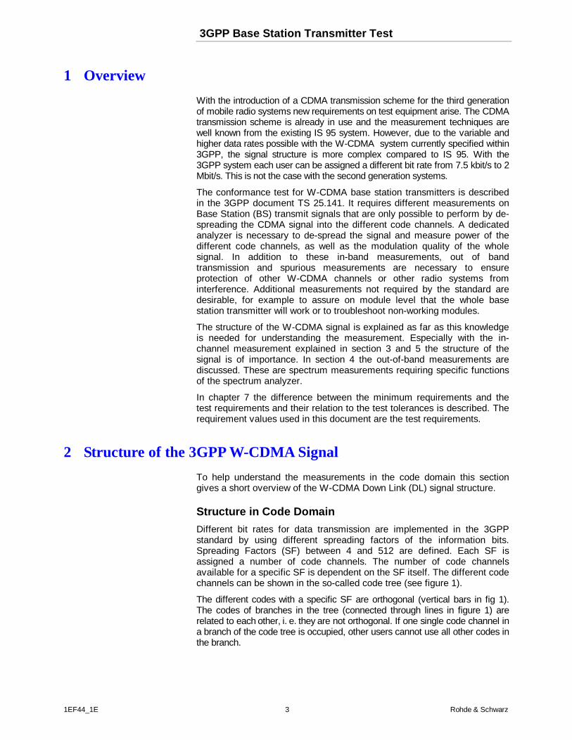
CPICH Power Accuracy
The purpose of this test is to verify that the CPICH power matches, withinthe limits given in TS 25.141 (± 2.9 dB), the power signalled from thenetwork to the base station.
With the code domain power analyzer, the power of the P-CCPCH and theP-CPICH must be measured while the base station is transmitting with themaximum power and inner loop power control is disabled. For themeasurement of the CPICH power accuracy test model 2 is used.
The CPICH Power can easily be measured with the FSIQ by using themarker. After analyzing the signal in code domain power mode, the markeris set to the CPICH or the P-CCPCH by using the dedicated markerfunctions (MKR -> CPICH or MKR -> PCCPCH). The marker read outshows the respective power level (see marker output in figure 10).
B
dBm
Ref Lvl9 dBm
Ref Lvl9 dBm
Ref Lvl9 dBm
Ref Lvl9 dBm
START: CH 0 STOP: CH 51164 CH/DIV
-48
-41
A
-83
-76
-69
-62
-55
-48
-41
-27
-90
-201
©
Ref Lvl9 dBm
Ref Lvl9 dBm
Ref Lvl9 dBm
Ref Lvl9 dBm
RESULT SUMMARY
CF 2.1175 GHzResult SummaryResult Summary
CPICH Slot 0CPICH Slot 0
SR 15 kspsChan Code 0Chan Code 0
Chan Slot 0Chan Slot 0
Marker 1 [T1]-9.93 dBm
slot 0 SR 15 ksps chan 0
CF 2.1175 GHzCode Pwr AbsoluteCode Pwr AbsoluteCPICH Slot 0CPICH Slot 0
SR 15 kspsChan Code 0Chan Code 0Chan Slot 0Chan Slot 0
GLOBAL RESULTSTotal PWR 0.06 dBmChip Rate Err -0.04 ppmIQ Offset 0.23 %Modulation Acc 2.62 % rmsCPICH Slot Number 0
Carr Freq Err 81.01 HzTrg to Frame -2.18 msIQ Imbalance 0.56 %Pk Code Dom Err -52.19 dB rms
( 15 ksps)
Timing Offset 0 ChipsChan Slot Number 0
Error Vector Mag 0.64 % PkChan Pow abs. -9.93 dBm
CHANNEL RESULTSSymb Rate 15 kspsChannel Code 0Chan Pow rel. 0.00 dBError Vector Mag 0.37 % rms
Fig 10 Code domain power display with the marker readout for CPICHpower. Test model 2 signal used.
The absolute power is output also in the RESULT SUMMARY in theCHANNEL RESULT section.
Frequency Stability
With the frequency stability measurement the correct frequency of the basestation is to be verified. The requirement is a frequency accuracy of 0.05 ppmof the set transmit frequency. The standard only requires that the transmitsignal is continuously modulated. No specific channel configuration is stated inthe standard.
The FSIQ can measure the frequency error of the base station in any channelconfiguration. Along with the RESULT SUMMARY the frequency error isalways output in the GLOBAL RESULTS table (see figure 10, Carr Freq Err). Itis calculated during synchronization to the W-CDMA signal.

3GPP Base Station Transmitter Test
1EF44_1E 12 Rohde & Schwarz
However, for highest accuracy the FSIQ needs a high precision externalreference fulfilling the high stability requirements. Oven controlled crystaloscillators normally do not provide sufficient stability to meet the requirement.An external reference signal, for example a Rubidium oscillator, is necessary tosynchronize the internal reference oscillator of the FSIQ.
Power Control Steps and Combined Power Control Tolerance
Control of output power is important in CDMA systems. To minimizeinterference with other users the transmitted power in each code channel shouldbe kept at its minimum for a reliable connection. The mobile station thereforesends a power control message (TPC bits, see figure 2) to the base station ineach timeslot to request the base station to decrease or increase the transmitpower.
The base station needs to adjust the power of an individual code channelin 1-dB steps (optional 0.5-dB steps) dependent on the power controlsymbol sent by the mobile station. In order to minimize the interference toother users, the transmit power of the base station must be set veryaccurately. The accuracy of the 1-dB steps is required to be ± 0.6 dB andfor the optional 0.5-dB steps the accuracy must be ± 0.35 dB.
After 10 consecutive steps in one direction the error of the relative power isrequired to be within a 2.1-dB tolerance for 1-dB steps and within a 1.1-dBtolerance for 0.5-dB steps.
Test model 2 is used for testing the power control steps.
The FSIQ evaluates a complete frame for code domain power measurement.Therefore, the measurement of the power control step tolerance and thecombined power control tolerance can be measured in a single run.
dB
-28
-21
A
Ref Lvl8 dBm
Ref Lvl8 dBm
Ref Lvl8 dBm
Ref Lvl8 dBm
START: CH 0 STOP: CH 51164 CH/DIV
dB
1CS
CPICH 15
Ref Lvl8 dBm
Ref Lvl8 dBm
Ref Lvl8 dBm
Ref Lvl8 dBm
0 16
-8
-6B
-63
-56
-49
-42
-35
-28
-21
-7
-70
0
-18
-16
-14
-12
-10
-8
-6
-2
-20
0
1
Marker 1 [T1]-4.04 dB
slot 0 SR 30 ksps chan 72
1
1
CS
Delta 1 [T2]-7.01 dB
slot 12
CF 2.1175 GHzPower vs SlotPower vs Slot
CPICH Slot 0CPICH Slot 0
SR 30 kspsChan Code 72Chan Code 72
Chan Slot 0Chan Slot 0
CF 2.1175 GHzCode Pwr RelativeCode Pwr Relative
CPICH Slot 0CPICH Slot 0
SR 30 kspsChan Code 72Chan Code 72
Chan Slot 0Chan Slot 0
Fig 11 Measurement of the 1-dB power control steps
3GPP Base Station Transmitter Test
1EF44_1E 13 Rohde & Schwarz
Using the marker and delta marker function in the time domain display theaccuracy of each power step can be measured directly with the delta markerreadout. Similarly, the relative power after 10 steps can be measured.
With the time domain display the relation between the CPICH and thecode channel under test can be checked. In figure 11 the power of codechannel 72 is controlled in 1-dB steps. The steps can be seen to be notaligned with the grid. This is due to the timing offset of channel 72 in testmodel 2. It is 7 x 256 chips = 1792 chips. The grid is instead aligned to theCPICH slots marked within the x-axis of the grid from 0 to 14. The verticalline marked with CS (Start Slot) shows the start of slot 0 of code channel72. The timeslot number of the displayed code channel is labeled belowthe grid (-1 to 15). Switching the display in the lower screen to ’ResultSummary’ outputs the measured timing offset (see e.g. figure 9).
The code levels shown in the upper part of the display in figure 11 aremeasured during the timeslot of the CPICH. As only 30% of code channel72 matches the CPICH slot the power read out by a marker set to codechannel 72 is 70% from the previous timeslot and 30 % from the selectedCPICH slot number. For accurate power measurement of code channelswith a timing offset the time domain display is the right choice.
Total Power Dynamic Range
The total power dynamic range is the difference between the maximumoutput power and the minimum output power of a base station for theentire signal. It is measured with test model 4. The base station outputsignal only consists of the CPICH, the P-CCPCH + SCH and the PICHchannel.
For testing the total power dynamic range the maximum output powermust first be measured. Then, all code channels are set to their minimumpower. The total power must be at least 18 dB below the maximum outputpower.
The total power dynamic range can be measured in the spectrum mode aswell as with the Code Domain Power function of the FSIQ. In spectrummode, the channel power function leads to faster results, as the codepower calculation within the FSIQ is not necessary. In code domain modein addition to the total power measurement, the correct code configurationof the device under test can be checked. For both possibilities the FSIQoffers one-button solutions. The level auto adjust function of the FSIQfrees the user from the need to manually optimize the analyzer inputsettings.
Power Control Dynamic Range
The purpose of the test is to verify the dynamic range of an individual codechannel. The code channel under test is set to its maximum power, and toits minimum power. At its maximum power the code channel must begreater than the total power of the signal –3.2 dB. Its minimum power mustbe less than the total power –27.8 dB.
The test is performed on traffic channels (DPCH) using test model 2. Ituses 3 traffic channels. The DPCH under test is set to its maximum powerlevel. The level of the other DPCHs is reduced to meet the requirement forthe DPCH under test to be greater than the total power - 3 dB. Then powerof the DPCH under test is set to its minimum power control level. Thepower of the other code channels remains unchanged. In this configurationthe level of the DPCH under test is measured.

3GPP Base Station Transmitter Test
1EF44_1E 14 Rohde & Schwarz
If the device under test can be commanded to set the power in 3-dB steps themeasurement can be carried out in a single run. If only 1-dB steps are possiblea two-pass measurement is necessary, the first pass at the maximum power ofthe code channel under consideration and the second pass at its minimumpower.
Figure 12 shows an example for measuring power control dynamic rangeby commanding the device under test in 3-dB steps. The Delta Markerreadout shows the level of code channel 72 after 9 steps.
dB
-18
-11
Ref Lvl8 dBm
Ref Lvl8 dBm
Ref Lvl8 dBm
Ref Lvl8 dBm
CF 2.1175 GHzCode Pwr RelativeCode Pwr RelativeCPICH Slot 0CPICH Slot 0
SR 30 kspsChan Code 72Chan Code 72Chan Slot 0Chan Slot 0
dB
0CS
CPICH 14
Ref Lvl8 dBm
Ref Lvl8 dBm
Ref Lvl8 dBm
Ref Lvl8 dBm
-1 15
CF 2.1175 GHz
Power vs SlotPower vs SlotCPICH Slot 0CPICH Slot 0
SR 30 ksps
Chan Code 72Chan Code 72Chan Slot 0Chan Slot 0
-6
-2
A
B
START: CH 0 STOP: CH 51164 CH/DIV
-26
-22
-18
-14
-10
-6
-2
6
-30
10
-53
-46
-39
-32
-25
-18
-11
3
-60
10
1
1
1
Delta 1 [T2]-27.00 dB
slot 11
CS
Marker 1 [T1]0.00 dB
slot 0 SR 15 ksps chan 0
Fig 12 Measurement of the power control dynamic range using 3-dB stepsfor code channel 72
Measurement of the Transmit Modulation Quality
Modulation Accuracy (EVM)
The Error Vector Magnitude (EVM) is defined as the difference between themeasured waveform and the theoretical modulated waveform. An errorvector is calculated from the difference of both waveforms for each chip.From the error vectors the Mean Error Vector Power (MEVP) is calculatedfor a complete timeslot. The MEVP is related to the Mean Reference SignalPower (MRSP) within the same slot. From these two power values the EVMis calculated as follows:
MRSPMEVP
EVM/% =
Test model 4 using the Paging Indication Channel (PICH) and theSynchronization Channels (SCH), only is applied. As the measurementinterval is specified to be one timeslot, the EVM result is one numberedvalue per timeslot. The specification of the EVM is valid over the totalpower dynamic range.

3GPP Base Station Transmitter Test
1EF44_1E 15 Rohde & Schwarz
As the Synchronization Channels in the test signal are not orthogonal tothe other code channels, they increase the EVM unless special measuresare taken to account for the distortion created by the SCH. Whencalculating the ideal waveform the FSIQ takes into account the non-orthogonal SCHs. That way both the ideal waveform and the measuredwaveform have the SCH included. This procedure results in an EVM valuethat represents the behavior of the device under test rather than the impactof the SCHs.
In general EVM can be measured for any code channel configuration.However, with different code channel configurations to test model 4, adifferent crest factor of the signal will result. For most realistic signals, e.g.test model 1 or 3, the crest factor will be higher and this will stress thedevice under test more.
The FSIQ needs the CPICH (optional in test model 4) to be available in theW-CDMA signal in order to synchronize to the W-CDMA waveform.Otherwise any code channel configuration can be used for EVMmeasurement. This allows for the modulation quality to be tested undervarious conditions to determine the impact of different loading conditionsto the device under test. The following screen-shot shows the EVMmeasurement using a W-CDMA signal loaded with 32 code channels (testmodel 3).
dB
-28
-21
Ref Lvl11 dBmRef Lvl11 dBmRef Lvl11 dBmRef Lvl11 dBm
START: CH 0 STOP: CH 51164 CH/DIV
A
%
Ref Lvl11 dBmRef Lvl11 dBmRef Lvl11 dBmRef Lvl11 dBm
0 15
CF 2.1175 GHzModulation Acc.Modulation Acc.CPICH Slot 0CPICH Slot 0
SR 15 kspsChan Code 100Chan Code 100Chan Slot 0Chan Slot 0
12
14B
-63
-56
-49
-42
-35
-28
-21
-7
-70
0
2
4
6
8
10
12
14
18
0
20
1
1
CS
Marker 1 [T1]0.00 dB
slot 0 SR 15 ksps chan 0
CF 2.1175 GHzCode Pwr RelativeCode Pwr Relative
CPICH Slot 0CPICH Slot 0
SR 15 kspsChan Code 100Chan Code 100
Chan Slot 0Chan Slot 0
Marker 1 [T2]2.470 %
slot 0
Fig 13 Graphic display of the EVM dependent on the slot number for acomplete frame
The EVM for all 15 slots of a W-CDMA frame is displayed graphically inthe lower part of the screen. The numbered values for the EVM can beread out easily using the marker.
Alternately the mean value for the EVM over all slots of the analyzedframe can be read in the GLOBAL RESULTS of the RESULT SUMMARY.

3GPP Base Station Transmitter Test
1EF44_1E 16 Rohde & Schwarz
B
CF 2.1175 GHzResult SummaryResult SummaryCPICH Slot 0CPICH Slot 0
SR 15 kspsChan Code 100Chan Code 100Chan Slot 0Chan Slot 0
Ref Lvl9 dBm
Ref Lvl9 dBm
Ref Lvl9 dBm
Ref Lvl9 dBm
RESULT SUMMARY
Carr Freq Err 81.44 HzTrg to Frame 2.64 msIQ Imbalance 0.40 %Pk Code Dom Err 51.79 dB rms
( 15 ksps)
GLOBAL RESULTSTotal PWR -0.00 dBmChip Rate Err -0.04 ppmIQ Offset 0.35 %Modulation Acc 2.83 % rmsCPICH Slot Number 0
CHANNEL RESULTSSymb Rate 15 kspsChannel Code 100Chan Pow rel. -5.01 dBError Vector Mag 1.03 % rms
Timing Offset 256 ChipsChan Slot Number 0Chan Pow abs. -15.98 dBmError Vector Mag 2.09 % Pk
Fig 14 Numeric display for the EVM of the complete frame in theRESULT SUMMARY
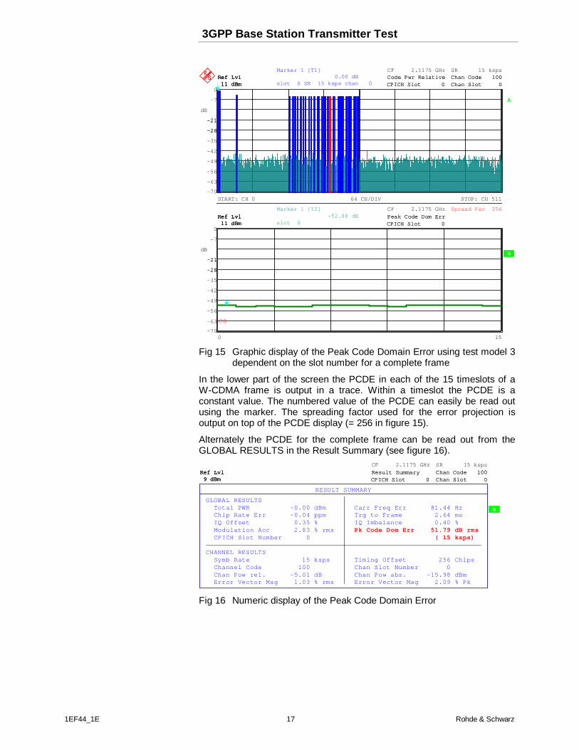
Peak Code Domain Error (PCDE)
With the PCDE measurement the difference between the test signal and theideal reference signal is projected onto the code space at a specific spreadingfactor. PCDE is a measure for the leakage of occupied code channels into allother channels. It represents the relative power leakage of non-ideal codechannels into free code channels. For Peak Code Domain Error (PCDE)measurement test model 3 is used. In addition to the organization channels ituses 16 or 32 traffic channels with a 15 kbps transmission rate each.
The TS25.141 standard specifies that the projection is made onto code channelswith spreading factor 256, i.e. 15 kbps transmission rate. The measurement hasto be performed on timeslot basis, i. e. for each slot one value or numberedresult is calculated. The FSIQ allows the user to select the spreading factor ofthe code channel for the projection of the error vector. That way the influence oncode channels with different spreading factors can be evaluated. A typical testresult for PCDE measurement with the Signal Analyzer FSIQ is shown in thefollowing figure.
3GPP Base Station Transmitter Test
1EF44_1E 17 Rohde & Schwarz
dB
-28
-21
Ref Lvl11 dBmRef Lvl11 dBmRef Lvl11 dBmRef Lvl11 dBm
START: CH 0 STOP: CH 51164 CH/DIV
CF 2.1175 GHzCode Pwr RelativeCode Pwr RelativeCPICH Slot 0CPICH Slot 0
SR 15 kspsChan Code 100Chan Code 100Chan Slot 0Chan Slot 0
dB
A
Ref Lvl11 dBmRef Lvl11 dBmRef Lvl11 dBmRef Lvl11 dBm
0 15
CF 2.1175 GHzPeak Code Dom ErrPeak Code Dom ErrCPICH Slot 0CPICH Slot 0
-28
-21B
-63
-56
-49
-42
-35
-28
-21
-7
-70
0
-63
-56
-49
-42
-35
-28
-21
-7
-70
0
1
1
CS
Marker 1 [T2]-52.88 dB
slot 0
Marker 1 [T1]0.00 dB
slot 0 SR 15 ksps chan 0
Spread Fac 256
Fig 15 Graphic display of the Peak Code Domain Error using test model 3dependent on the slot number for a complete frame
In the lower part of the screen the PCDE in each of the 15 timeslots of aW-CDMA frame is output in a trace. Within a timeslot the PCDE is aconstant value. The numbered value of the PCDE can easily be read outusing the marker. The spreading factor used for the error projection isoutput on top of the PCDE display (= 256 in figure 15).
Alternately the PCDE for the complete frame can be read out from theGLOBAL RESULTS in the Result Summary (see figure 16).
B
CF 2.1175 GHzResult SummaryResult SummaryCPICH Slot 0CPICH Slot 0
SR 15 kspsChan Code 100Chan Code 100Chan Slot 0Chan Slot 0
Ref Lvl9 dBmRef Lvl9 dBmRef Lvl9 dBmRef Lvl9 dBm
RESULT SUMMARY
Carr Freq Err 81.44 HzTrg to Frame 2.64 msIQ Imbalance 0.40 %Pk Code Dom Err 51.79 dB rms
( 15 ksps)
GLOBAL RESULTSTotal PWR -0.00 dBmChip Rate Err -0.04 ppmIQ Offset 0.35 %Modulation Acc 2.83 % rmsCPICH Slot Number 0
CHANNEL RESULTSSymb Rate 15 kspsChannel Code 100Chan Pow rel. -5.01 dBError Vector Mag 1.03 % rms
Timing Offset 256 ChipsChan Slot Number 0Chan Pow abs. -15.98 dBmError Vector Mag 2.09 % Pk
Fig 16 Numeric display of the Peak Code Domain Error

3GPP Base Station Transmitter Test
1EF44_1E 18 Rohde & Schwarz
4 Measurements in Spectrum Domain
Occupied Bandwidth (OBW)
Occupied Bandwidth (OBW) is a measure of the bandwidth containing99% of the total integrated power for transmitted spectrum and is centeredon the assigned channel frequency. The occupied channel bandwidth shallbe less than 5 MHz based on a chip rate of 3.84 Mcps.
For measurement of the OBW test model 1 is used.
The FSIQ measures the OBW using scalar spectrum analyzer mode. Bysetting up the OBW measurement with the dedicated function provided byFSIQ-K72, the FSIQ uses a pre-defined setting as specified in TS25.141.The total power is measured within a span of 10 MHz.
A
1RM
-100
-90
-80
-70
-60
-50
-40
-30
-20
-111
-11
1
T1
Marker 1 [T1]
-20.63 dBm
2.11749750 GHz
Ref Lvl
-11 dBm
Ref Lvl
-11 dBm
RBW 30 kHz
VBW 300 kHz
SWT 200 ms
RF Att 20 dB
Unit dBm
Center 2.1175 GHz 1 MHz/ Span 10 MHz
T2
1 [T1] -20.63 dBm
2.11749750 GHz
T1 [T1] -26.36 dBm
2.11546593 GHz
T2 [T1] -27.68 dBm
2.11953407 GHz
OPB 4.06813627 MHz
Fig 17 Measurement example for Occupied Bandwidth measurement
The FSIQ first measures the total power by integrating the pixels of thecomplete trace. The FSIQ then integrates the trace beginning with the startfrequency until the power is 0.5 % of the total power. Finally it integratesthe trace beginning with the stop frequency until 0.5 % of the total power isreached. The OBW is calculated from both frequencies at the 0.5-% powerpoint.
Spectrum Emission Mask
The Spectrum Emission Mask measurement defines a mask in a 25 MHzspan, which must be met by a base station output signal. Close to thecarrier a 30 kHz measurement bandwidth is used whereas far off thecarrier a 1 MHz bandwidth is used. Test model 1 is specified in TS25.141for the measurement.

3GPP Base Station Transmitter Test
1EF44_1E 19 Rohde & Schwarz
The following figure shows the limits and the associated measurementbandwidths dependent on the frequency offset from the transmit channel:
-15
-20
-25
-30
-35
-40
Frequency offset ∆ f from the carrier [MHz]
2.5 2.7 3.5 ∆f max7.5
P = 43 dBmP = 43 dBm
RBW = 1 MHz
P = 39 dBmP = 39 dBm
P = 31 dBmP = 31 dBm
-10
P = 31 dBmP = 31 dBm
P = 43 dBmP = 43 dBm
Limit [dBm]
RBW = 30 kHz
Fig 18 Limits for the spectrum emission mask measurement
The test limits are dependent on the output power of the base station. Withmost spectrum analyzers, using 4- or 5-pole Resolution Bandwidth (RBW)filters the selectivity of the 1-MHz RBW filter causes leakage of thetransmit signal close to the carrier at 3.5 MHz offset. Using a 1-MHzresolution bandwidth, leakage power due to the filter characteristic ismeasured rather than leakage power due to the signal itself.
The standard TS25.141 therefore allows simulating the 1-MHzmeasurement bandwidth by using a narrow resolution bandwidth andintegration over 1 MHz. This so-called Integrated Bandwidth method (IBW)gives true results for the average power in the 1 MHz bandwidth. However,peak power due to transients cannot be measured correctly.
The FSIQ-K72 automatically detects, based on the input power, what testlimit to apply and reports if the test has been passed or failed according tothe 3GPP limits. The user also has the option to define which power classlimits to test against, or even to define the limits.

3GPP Base Station Transmitter Test
1EF44_1E 20 Rohde & Schwarz
A
RBW 30 kHz
VBW 300 kHz
SWT 500 ms
RF Att 30 dB
Mixer -20 dBm
1RM
Unit dBm
43 dB Offset
Ref Lvl
45 dBm
Ref Lvl
45 dBm
2.5 MHz/Center 2.1 GHz Span 25 MHz
-50
-40
-30
-20
-10
0
10
20
30
40
-55
45
1
Marker 1 [T1]
-33.66 dBm
2.09616000 GHz
1 [T1] -33.66 dBm
2.09616000 GHz
CH PWR 43.15 dBm
CH BW 3.84000000 MHz
LIMIT CHECK : PASSED
C0C0
P>=43
Fig 19 Measurement of the Spectrum emission mask using the FSIQ-K72
Measurement of the Adjacent Channel Leakage Ratio (ACLR)
For Adjacent Channel Leakage Ratio measurement (ACLR) test model 1 isused. ACLR is defined as the ratio of the average power in the transmitchannel to the power in the 5-MHz and 10-MHz offset channels, eachmeasured with a 3GPP receive filter (root raised cosine filter, α = 0.22 andfchip = 3.84 Mcps). The standard states that a true rms voltage or anaverage power measurement method must be used. The stability of thetest result shall be ≤ 0.2 dB at a 95 % confidence level. A favorablemethod to accomplish this is the use of a rms detector in a spectrumanalyzer. It measures the true average power during a settable time frame.
The Signal Analyzer FSIQ provides a pre-defined test routine for ACLRmeasurement on 3GPP signals using the rms detector. It calculates therequired root raised cosine filter by weighting the trace pixels beforeintegrating them for the power in the different channels. The stability of thetest result is influenced by the set sweeptime.
When measuring all 5 channels specified in the standard a sweeptime of500 ms leads to a standard deviation of the ACLR values of 0.1 dB. Thiscorresponds to 0.2-dB stability with a 95 % confidence level.

3GPP Base Station Transmitter Test
1EF44_1E 21 Rohde & Schwarz
2.46848 MHz/Center 2.1175 GHz Span 24.6848 MHz
-100
-90
-80
-70
-60
-50
-40
-30
-20
-111
-11
1
cl2cl2
cl1cl1
C0C0
cu1cu1
cu2cu2
Marker 1 [T1]
-20.31 dBm
2.11749750 GHz
RBW 30 kHz
VBW 300 kHz
SWT 2 s
RF Att 20 dB
Unit dBm
Ref Lvl
-11 dBm
Ref Lvl
-11 dBm
1 [T1] -20.31 dBm
2.11749750 GHz
CH PWR -0.02 dBm
ACP Up -56.81 dB
ACP Low -56.82 dB
ALT1 Up -57.93 dB
ALT1 Low -58.01 dB
Fig 20 Measurement of the Adjacent Channel Leakage Ratio using theFSIQ
In the 3GPP standard (TS 25.141, Ver. 3.5.0) the following ACLR valuesare mandatory at the antenna connector of the base station:
Channel offset ACLR
± 5 MHz -44.2 dBc
± 10 MHz -49.2 dBc
For the analyzer not to influence the ACLR value the inherent ACLRshould be about 10 dB lower than the specified limits to measure. With 10dB margin the error introduced by the analyzer is +0.41 dB.
As all stages of the transmitter chain contribute to the total ACLR at the basestation output, in general the ACLR values of the different stages need to belower. This sets higher requirements for the inherent ACLR of the analyzer.
In the 2-GHz frequency range the FSIQ provides an inherent ACLR of -75 dBcin the 5-MHz offset channel at the optimum mixer level1 of about -12 dBm.Taking the 10-dB step-size of the input attenuator into consideration theinherent ACLR is - 71 dBc in the worst case within the mixer level rangebetween -8 and -18 dBm. For higher requirements a 1-dB step attenuator(option FSE-B13) can be added to the FSIQ to meet the optimum level (-12dBm) of the mixer for any level at the RF input. In the 10-MHz offset channelthe respective value is -81 dBc at the optimum mixer level of -3 dBm. Theassumed crest factor of the W-CDMA signal is 11 dB for these values.
For details of ACLR measurement using FSE Spectrum Analyzers see [3].
1 Mixer level = level at the RF connector of the analyzer - RF attenuation

3GPP Base Station Transmitter Test
1EF44_1E 22 Rohde & Schwarz
5 Additional Useful Code Domain Measurements
In addition to the measurements required for the conformance testaccording to TS 25.141 other measurements are very helpful whiledeveloping base stations or their modules, and for trouble-shooting.
For a quick check of the organization part of a channel, viewing thebitstream within a slot is very helpful. The FSIQ outputs the detectedbitstream for the selected code channel and timeslot.
dB
-28
-21
A
B
START: CH 0 STOP: CH 51164 CH/DIV
Ref Lvl8 dBmRef Lvl8 dBmRef Lvl8 dBmRef Lvl8 dBm
CF 2.1175 GHzBitstreamBitstreamCPICH Slot 0CPICH Slot 0
SR 240 kspsChan Code 13Chan Code 13Chan Slot 0Chan Slot 0
-63
-56
-49
-42
-35
-28
-21
-7
-70
0
1
Marker 1 [T1]-50.89 dB
slot 0 SR 7.5 ksps chan 289
BITSTREAM
0 10 10 01 00 01 11 00 01 10 11 01 01 01 11 00 0116 00 11 00 01 00 01 00 00 00 00 10 0032 01 00 01 10 00 01 00 11 10 01 01 0148 01 10 00 01 10 11 11 01 00 11 01 11 00 10 00 1064 10 00 01 01 01 10 10 01 11 11 10 11 00 10 01 0080 10 11 01 11 11 10 01 00 11 01 01 00 11 00 11 0096 00 00 01 10 00 11 00 10 10 00 11 01 00 10 11 11
112 11 10 10 00 10 11 00 01 11 01 01 10 01 01 10 01128 11 10 00 11 11 10 11 10 10 00 00 11 01 01 10 11144 01 11 01 10 00 00 10 11 11 11 11 10
Marker 1 [T2] 5 symValue 11
CF 2.1175 GHzCode Pwr RelativeCode Pwr RelativeCPICH Slot 0CPICH Slot 0
SR 240 kspsChan Code 13Chan Code 13Chan Slot 0Chan Slot 0
Ref Lvl8 dBmRef Lvl8 dBmRef Lvl8 dBmRef Lvl8 dBm
TPC bits
Pilot bitsTFCI bits
11 11 11 11
11 11 11 10
-- -- -- --
Fig 21 Bitstream Output of the dedicated physical channel 13 using asymbol rate of 240 kbps, timeslot 0
The example in figure 21 shows the bitstream in slot 0 of code channel 13with a symbol rate of 240 kbit/s. No TFCI bits (Transport FormatCombination Indicator) have been transmitted in this channel. Thereforeon the positions of the TFCI bits ’-’ are output as the FSIQ could not detectvalid symbols.

3GPP Base Station Transmitter Test
1EF44_1E 23 Rohde & Schwarz
Symbol Constellation Diagram
For each channel a constellation diagram of the de-spread symbols can bedefined. As a measure of the quality of the specific code channel an EVMat the symbol level is helpful as a numbered value. From both, the impactof a non-ideal transmission block on an individual user channel can beseen.
Figure 22 shows an example for a constellation diagram of code channel72 marked red in the code domain display. The signal under test has beenclipped in baseband in front of the transmit filter.
dB
-28
-21
A
Ref Lvl8 dBmRef Lvl8 dBmRef Lvl8 dBmRef Lvl8 dBm
START: CH 0 STOP: CH 51164 CH/DIV
Ref Lvl8 dBmRef Lvl8 dBmRef Lvl8 dBmRef Lvl8 dBm
-4.1666667 4.1666667
CF 2.1175 GHzSymbol Const DiagSymbol Const Diag
CPICH Slot 0CPICH Slot 0
SR 30 kspsChan Code 72Chan Code 72
Chan Slot 0Chan Slot 0
B
-63
-56
-49
-42
-35
-28
-21
-7
-70
0
-1.5
1.5
1
1
Marker 1 [T1] 5.00Real 650.273 mImag -651.136 m
Marker 1 [T1]-3.55 dB
slot 0 SR 30 ksps chan 72
CF 2.1175 GHzCode Pwr RelativeCode Pwr Relative
CPICH Slot 0CPICH Slot 0
SR 30 kspsChan Code 72Chan Code 72
Chan Slot 0Chan Slot 0
Fig. 22 Constellation diagram of code channel 72 and code domain powerof a W-CDMA signal with clipping.
Due to the clipping, energy from the used code channels is spread intoinactive code channels. The clipping can be seen more clearly in thesymbol constellation diagram. Some of the constellation points show alower magnitude than expected from an ideal signal.
3GPP Base Station Transmitter Test
1EF44_1E 24 Rohde & Schwarz
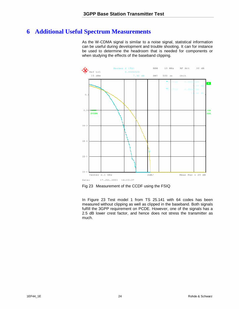
6 Additional Useful Spectrum Measurements
As the W-CDMA signal is similar to a noise signal, statistical informationcan be useful during development and trouble shooting. It can for instancebe used to determine the headroom that is needed for components orwhen studying the effects of the baseband clipping.
A
RBW 10 MHz
SWT 500 Ës
RF Att 30 dB
1SA
Unit
Ref Lvl
15 dBm
Ref Lvl
15 dBm
Center 2.1 GHz Mean Pwr + 20 dB2dB/
2SA
1AVG
2VIEW
0.1
0.01
1E-3
1E-4
1E-5
1E-6
1
1
2
Marker 2 [T2]
0.0000020
7.90 dB
2 [T2] 0.0000020
7.90 dB
1 [T1] 0.0000190
10.40 dB
Date: 17.JUL.2001 14:23:37
Fig 23 Measurement of the CCDF using the FSIQ
In Figure 23 Test model 1 from TS 25.141 with 64 codes has beenmeasured without clipping as well as clipped in the baseband. Both signalsfulfill the 3GPP requirement on PCDE. However, one of the signals has a2.5 dB lower crest factor, and hence does not stress the transmitter asmuch.

3GPP Base Station Transmitter Test
1EF44_1E 25 Rohde & Schwarz
7 Test Tolerances
In contrast to most mature mobile communication standards, 3GPP hasseparated the system requirements and the test requirements. Theconcept makes use of minimum requirements, test requirements and testtolerances.
The minimum requirements are requirements that do not take uncertaintiesintroduced by test and measurement into account and can be seen assystem requirements. These requirements are also frequently called corerequirements. The test requirements are the minimum requirementsrelated with the maximum acceptable test tolerance. The test requirementscontain the values with which the result of a test shall be compared inorder to determine the outcome of that test. The test tolerance is eitherequal to the maximum acceptable test uncertainty or it is set to zero.Requirements that are based on regulatory requirements, such as the ITU-R recommendation SM329-8 on spurious emission, or where the testsystem uncertainty could not be determined, have a zero test tolerance. Ifa test system has a higher uncertainty than the maximum acceptable, thetest tolerance is reduced by the value by which it exceeds the acceptableuncertainty.
Regardless of how the test system uncertainty is applied in the standardfor the test requirements, low test system uncertainties always have thebenefit of more stabile and repeatable results. For the requirements withnon-zero test tolerance, a lower than specified test system uncertainty, the3GPP concept provides additional margins for the design.
8 Abbreviations
3GPP Third generation partnership projectACLR Adjacent Channel Leakage RatioCCDF Complementary Cumulative Distribution FunctionCPICH Common Pilot ChannelDCCH Dedicated Control ChannelDPCCH Dedicated Physical Control ChannelDPCH Dedicated Physical ChannelDPDCH Dedicated Physical Data ChannelDTCH Dedicated Traffic ChannelEVM Error Vector MagnitudeFACH Forward Access ChannelITU International Telecommunication Union.PICH Paging Indication ChannelPCCPCH Primary Common Control Physical ChannelPCDE Peak Code Domain ErrorPCH Paging ChannelPSCH Primary Synchronization channelSCCPCH Secondary Common Control Physical ChannelSCH Synchronization ChannelSSCH Secondary Synchronization ChannelTFCI Transport Format Combination IndicatorTPC Transmit Power Control

3GPP Base Station Transmitter Test
1EF44_1E 26 Rohde & Schwarz
9 Literature
[1] Technical Specification TS 25.104 V 4.0.0, 3rd Generation PartnershipProject (3GPP), Technical Specification Group (TSG) RAN WG4,UTRA (BS) FDD; Radio transmission and Reception
[2] Application Note 1GP39_0E, W-CDMA Signal Generator Solutions byRohde & Schwarz
[3] Application Note 1EF40_E, Measurement of Adjacent Channel Poweron Wideband CDMA Signals
[4] Josef Wolf and Bob Buxton, ”Measure Adjacent Channel Power With aSpectrum Analyzer, ” Microwaves & RF, January 1997, pp. 55-60.
10 Ordering information
Type of instrumentOrdering number
FSIQ3 20 Hz to 3.5 GHz 1119.5005.13FSIQ7 20 Hz to 7 GHz 1119.5005.17FSIQ26 20 Hz to 26.5 (27) GHz 1119.6001.27FSIQ-B70 DSP and IQ Memory Extension 1119.6747.02FSIQ-K72 Application Firmware 3GPP
Code Domain Power Measure-ment for FSIQ
1126.4746.02
ROHDE & SCHWARZ GmbH & Co. KG . Mühldorfstraße 15 . D-81671 München . P.O.B 80 14 69 . D-81614 München .
Telephone +49 89 4129 -0 . Fax +49 89 4129 - 13777 . Internet: http://www.rohde-schwarz.com
This application note and the supplied programs may only be used subject to the conditions of use set forth in the downloadarea of the Rohde & Schwarz website.