July 2011 doc.: IEEE 802.15/0463 Project: IEEE P802.15 ...€¦ · Abstract: Graphene is emerging...
29
doc.: IEEE 802.15/0463 Submission July 2011 <Xiangfeng Duan>, <UCLA> Slide 1 Project: IEEE P802.15 Working Group for Wireless Personal Area N Project: IEEE P802.15 Working Group for Wireless Personal Area N etworks ( etworks ( WPANs WPANs ) ) Submission Title: Approaching Terahertz Transistors with Graphene Date Submitted: 18 July, 2011 Source: Xiangfeng Duan Company: Department of Chemistry and Biochemistry,3California Nanosystems Institute, University of California, Los Angeles, California 90095, USA Address: 607 Charles E Young Dr., Los Angeles, CA 90095 Voice:3102674947, E-Mail: [email protected] Abstract: Graphene is emerging as an attractive electronic material for ultra-high speed electronics due to its exceptionally high carrier mobility and saturation velocity. However, the conventional dielectric integration and device fabrication processes cannot be readily applied to graphene transistors because they can often introduce substantial defects into the monolayer of carbon lattices and severely degrade the device performance. Here I will discuss the opportunities, challenges and recent progresses in exploring graphene for high speed transistors. Purpose: Overview of the potential of graphene for terahertz electronics. Notice: This document has been prepared to assist the IEEE P802.15. It is offered as a basis for discussion and is not binding on the contributing individual(s) or organization(s). The material in this document is subject to change in form and content after further study. The contributor(s) reserve(s) the right to add, amend or withdraw material contained herein. Release: The contributor acknowledges and accepts that this contribution becomes the property of IEEE and may be made publicly available by P802.15.
Transcript of July 2011 doc.: IEEE 802.15/0463 Project: IEEE P802.15 ...€¦ · Abstract: Graphene is emerging...

doc.: IEEE 802.15/0463
Submission
July 2011
<Xiangfeng Duan>, <UCLA>Slide 1
Project: IEEE P802.15 Working Group for Wireless Personal Area NProject: IEEE P802.15 Working Group for Wireless Personal Area Networks (etworks (WPANsWPANs))
Submission Title: Approaching Terahertz Transistors with GrapheneDate Submitted: 18 July, 2011Source: Xiangfeng DuanCompany: Department of Chemistry and Biochemistry,3California Nanosystems Institute, University of California, Los Angeles, California 90095, USAAddress: 607 Charles E Young Dr., Los Angeles, CA 90095Voice:3102674947, E-Mail: [email protected]: Graphene is emerging as an attractive electronic material for ultra-high speed electronics due to its exceptionally high carrier mobility and saturation velocity. However, the conventional dielectric integration and device fabrication processes cannot be readily applied to graphene transistors because they can often introduce substantial defects into the monolayer of carbon lattices and severely degrade the device performance. Here I will discuss the opportunities, challenges and recent progresses in exploring graphene for high speed transistors.
Purpose: Overview of the potential of graphene for terahertz electronics.Notice: This document has been prepared to assist the IEEE P802.15. It is offered as a basis for discussion and is not binding on the contributing individual(s) or organization(s). The material in this document is subject to change in form and content after further study. The contributor(s) reserve(s) the right to add, amend or withdraw material contained herein.Release: The contributor acknowledges and accepts that this contribution becomes the property of IEEE and may be made publicly available by P802.15.
doc.: IEEE 802.15/0463
Submission
Xiangfeng Duan
Department of Chemistry and Biochemistry
University of California, Los [email protected]
Xiangfeng Duan
Department of Chemistry and Biochemistry
University of California, Los [email protected]
Approaching Terahertz Transistors with Graphene
Approaching Terahertz Transistors Approaching Terahertz Transistors with with GrapheneGraphene
<Xiangfeng Duan>, <UCLA>
July 2011
doc.: IEEE 802.15/0463
Submission
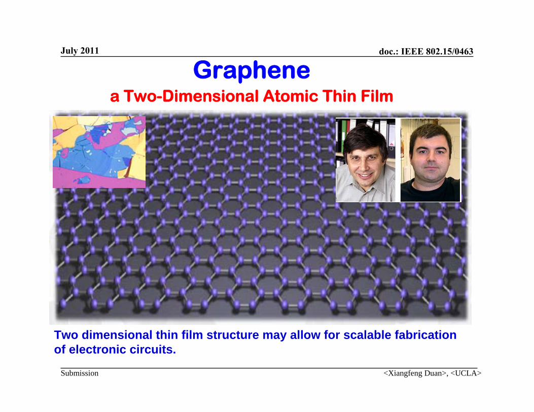
Graphenea Two-Dimensional Atomic Thin Film
Two dimensional thin film structure may allow for scalable fabrication of electronic circuits.
<Xiangfeng Duan>, <UCLA>
July 2011

doc.: IEEE 802.15/0463
Submission
Large Area Graphene
Nature Nanotech. 5, 574 (2010)
With just a few years of development, we have seen tremendous development with >30” single layer graphene now possible using CVD.
<Xiangfeng Duan>, <UCLA>
July 2011

doc.: IEEE 802.15/0463
Submission
Graphene for High Speed ElectronicsSingle atomic thicknessHighest carrier mobility up to 200,000 -1,000,000 cm2 V−1s−1
Highest saturation velocity (~5.5×107 cm/s)High thermal conductivity (~5,000 Wm−1K−1)Exceptional mechanical strength and flexibility Optically transparencyChemically inertness
<Xiangfeng Duan>, <UCLA>
July 2011

doc.: IEEE 802.15/0463
Submission
Challenges to High performance Graphene Transistors 1. New approaches for material integration and device fabrication
2. Induce a band‐gap: graphene nanostructures
Nanoribbon: Nano Lett., 9, 2083 (2009); 10 , 4590; 11, 1082 (2011) Nature Nano 5, 655, (2010).
Nanomesh: Nature Nano 5, 190, (2010); Chem Phys. Lett. 498,334 (2010).
Dielectric integration: PNAS, 107, 6711: Adv. Mater. 22, 2941; Nano Lett. 10 , 1917; 11 , 2555.
0.34 n
m
Al 2O3 n
anorib
bonSiO 2 Graphen
e
2 nm
Device fabrication: Nature, 467, 305;Nano Lett. 10 , 3952 ,NanoLett. 10.1021/nl201922c
HfO2
GNR
Si NW
2 nm
S DG
50nmgraphene
<Xiangfeng Duan>, <UCLA>
July 2011

doc.: IEEE 802.15/0463
Submission
Challenges to High performance Graphene Transistors
To form a transistor requires effective integration with other material components including gate dielectrics and source drain contacts.
Conventional electronic fabrication processes cannot be readily applied to graphene as many of these processes steps could create substantial damage to single atomic layer gaphene.
Alterative material integration or device fabrication strategies are needed to retain the high electronic performance and truly capitalize the intrinsic merit of graphene.
Semiconductor channel(high temperature growth)
Gate dielectrics(oxidation, deposition)
Source, drain contact(Implantation, anneal)
<Xiangfeng Duan>, <UCLA>
July 2011
doc.: IEEE 802.15/0463
SubmissionJACS 130, 8152 (2008).
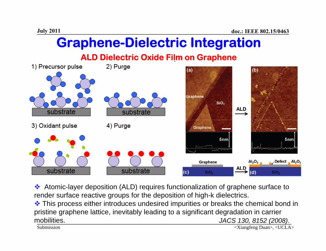
Graphene-Dielectric IntegrationALD Dielectric Oxide Film on Graphene
Atomic-layer deposition (ALD) requires functionalization of graphene surface to render surface reactive groups for the deposition of high-k dielectrics.
This process either introduces undesired impurities or breaks the chemical bond in pristine graphene lattice, inevitably leading to a significant degradation in carrier mobilities.
<Xiangfeng Duan>, <UCLA>
July 2011

doc.: IEEE 802.15/0463
SubmissionACS Nano, 2, 1033 (2008).
Graphene-Dielectric IntegrationPVD Dielectric Oxide Film on Graphene
Physical vapor deposition (PVD) such as electron-beam evaporation or sputtering process often results in lower quality dielectrics and also significant damages to graphene layer.
defect
<Xiangfeng Duan>, <UCLA>
July 2011

doc.: IEEE 802.15/0463
Submission
Top Gate Dielectrics Mobility before Deposition
Mobility after Deposition
Al2O3 by ALD 1200 cm2/V⋅s 400 cm2/V⋅s
SiO2 by evaporation 4790 cm2/V⋅s 790 cm2/V⋅s
SiO2 by evaporation 1700 cm2/V⋅s 500 cm2/V⋅s
HfO2 by ALD 2400 cm2/V⋅s 1200 cm2/V⋅s
The mobility values observed in the top‐gated devices to date are often nearly one order of magnitude smaller than what can be achieved in the back‐gated devices
HfO2 by ALD with polymer buffer layer: ~ 7600 cm2/V⋅s
Nano Lett. 9, 422 (2009); Nano Lett. 9, 4474 (2009); Appl. Phys. Lett. 95, 033103 (2009); IEEE Electron Dev. Lett. 28, 282 (2007); Nat. Nanotech. 3, 654 (2008); Appl. Phys. Lett. 94, 062107 (2009).
Substantial Mobility Degradation in Top-
Gated Devices
<Xiangfeng Duan>, <UCLA>
July 2011
doc.: IEEE 802.15/0463
Submission
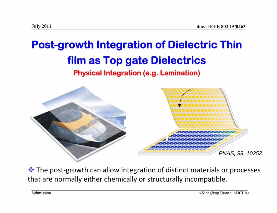
Post-growth Integration of Dielectric Thin
film as Top gate DielectricsPhysical Integration (e.g. Lamination)
The post‐growth can allow integration of distinct materials or processes that are normally either chemically or structurally incompatible.
PNAS, 99, 10252.
<Xiangfeng Duan>, <UCLA>
July 2011
doc.: IEEE 802.15/0463
Submission
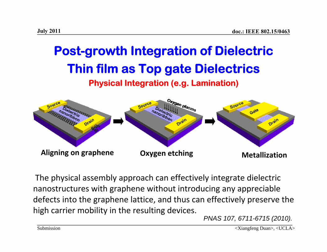
Post-growth Integration of Dielectric Thin film as Top gate Dielectrics
Physical Integration (e.g. Lamination)
Aligning on graphene Oxygen etching Metallization
The physical assembly approach can effectively integrate dielectric nanostructures with graphene without introducing any appreciable defects into the graphene lattice, and thus can effectively preserve the high carrier mobility in the resulting devices.
PNAS 107, 6711-6715 (2010).<Xiangfeng Duan>, <UCLA>
July 2011

doc.: IEEE 802.15/0463
Submission
Single crystalline, Smooth surface, High dielectric constant
110
B
5 nm1 μm
A
110
100 nm 5 nmC D
Al2O3 Nanoribbon
PNAS 107, 6711-6715 (2010).<Xiangfeng Duan>, <UCLA>
July 2011

doc.: IEEE 802.15/0463
Submission
Ti
SiO2
Ti
Al2O3 NRTi
SiO2
Ti
Al2O3 NR
0 2 4 6 8
10-7
10-6
10-5
10-4
10-3
J (A
/cm
2 )
E (M V / c m)0.0 0.2 0.4 0.6
-20
-18
-16
-14
-12
ln(J
/E2 )
1/E
Dielectric Properties of Al2O3 Nanoribbon
The current‐voltage (I‐V) measurements show typical Fowler–Nordheim (F‐N) tunnelling behaviour with a breakdown field of 8.5 MV/cm, comparable to/better than best reported ALD Al2O3 film.
)/exp(2OXOX EBAEJ −=
⎭⎬⎫
⎩⎨⎧
Φ×= −
BmA *
6 11054.1
2/32/1*7 )()(1083.6 BmB Φ×=
J : current densityEox : oxide electric fieldm* : effective mass of the charge carrier ~0.23meΦB : barrier height
ΦB (Ti/Al2O3) = 2.0 eV
MIM device
ɛ(Al2O3) = 8.5
<Xiangfeng Duan>, <UCLA>
July 2011

doc.: IEEE 802.15/0463
Submission
Integration of Graphene and Nanoribbon
2000 3000
2D
Inte
nsity
(a.u
.)
Raman shift (cm-1)
a b
Gba
ACS Nano, 2, 1033 (2008)
Raman studies clearly demonstrate that the room‐temperature physical assembly approach to integrate oxide nanostructures with graphene does not introduce any appreciable defects into the graphene lattice.
<Xiangfeng Duan>, <UCLA>
July 2011

doc.: IEEE 802.15/0463
Submission
S G
D
Al 2O3 nanorib
bonSiO 2
Ti
Graphene
Au0.3
4 nm
Al 2O3 nan
oribbon
SiO 2 Graphen
e
2 nm
Seamless Integration between Graphene and Nanoribbon
Cross‐sectional TEM studies show that there are no gaps or other impurities at the graphene/dielectric interface.
PNAS 107, 6711-6715 (2010).<Xiangfeng Duan>, <UCLA>
July 2011

doc.: IEEE 802.15/0463
Submission
-2 0 2
400
600
800
-40-20 0 20 40
400
600
800
VBG (V)
I ds
(μA
)
VTG (V)
I ds
(μΑ
)
Top-gated Graphene Transistor
Top-gated device exhibits typical transistor characteristics with a max gm of about 290 mS, which is more than 15 times larger than that of the back-gated device (gm ~19.5 mS).
The derived mobility value reaches 22,400 cm2/V·s using the constant mobility model:
0.0 0.5 1.00
200
400
600 -1.5 V -1.0 V -0.5 V 0.0 V 0.5 V
Vg (V)
I ds
(μA
)
Vds
PNAS 107, 6711-6715 (2010).
-2 -1 0 1 21.5k
2.0k
2.5k
VTG-VTG_Dirac (V)
Rto
t (oh
m)
Experimental data Fitting line
μneWLRRRR contactchannelcontacttot
/+=+=
<Xiangfeng Duan>, <UCLA>
July 2011
doc.: IEEE 802.15/0463
Submission
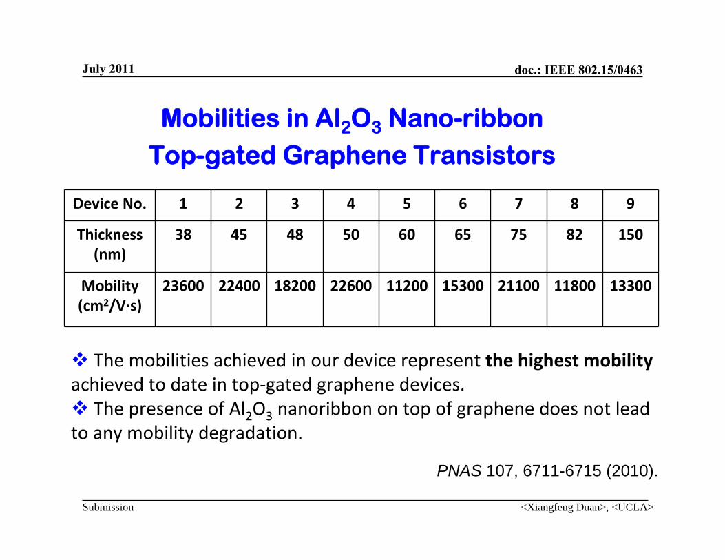
Device No. 1 2 3 4 5 6 7 8 9
Thickness(nm)
38 45 48 50 60 65 75 82 150
Mobility(cm2/V∙s)
23600 22400 18200 22600 11200 15300 21100 11800 13300
Mobilities in Al2O3 Nano-ribbonTop-gated Graphene Transistors
The mobilities achieved in our device represent the highest mobility achieved to date in top‐gated graphene devices.
The presence of Al2O3 nanoribbon on top of graphene does not lead to any mobility degradation.
PNAS 107, 6711-6715 (2010).
<Xiangfeng Duan>, <UCLA>
July 2011

doc.: IEEE 802.15/0463
Submission
Towards a High Speed TransistorAccess Resistance
Substantial access resistance due to the significant gaps between the source-gate and gate-drain electrodes, where a large portion of the graphene channel in the gap area is not gated.
With the size of the device shrinking into the deep nanometer regime, there is an increasing need for a more precise and reliable device fabrication process.
Cutoff Frequency:
m
g
drift
gatet g
CL==
ντ
g
m
gate
drift
tcT,intrinsi
Cg
L
f
ππν
πτ
22
21
==
=
<Xiangfeng Duan>, <UCLA>
July 2011
doc.: IEEE 802.15/0463
Submission
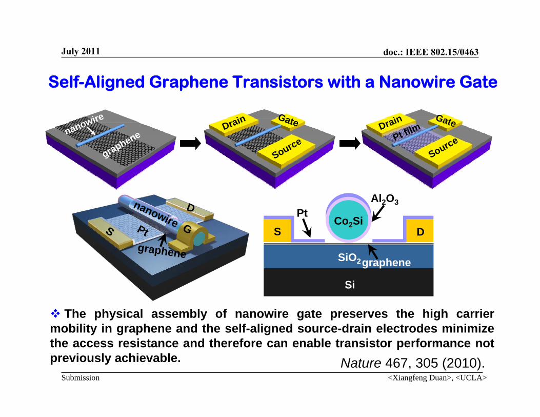
Self-Aligned Graphene Transistors with a Nanowire Gate
S GPtgraphene
nanowireD
SiO2
Si
graphene
PtS D
Al2O3
Co2Si
The physical assembly of nanowire gate preserves the high carrier mobility in graphene and the self-aligned source-drain electrodes minimize the access resistance and therefore can enable transistor performance not previously achievable.
graphenenanowireDrain
Source
GatePt film
Drain
Source
Gate
Nature 467, 305 (2010).<Xiangfeng Duan>, <UCLA>
July 2011
doc.: IEEE 802.15/0463
Submission
-0.10 -0.05 0.00 0.05 0.10-200
-100
0
100
200
Cur
rent
(μA
)
Voltage (V)
2 electrodes 4 electrodes
Al2O3Co2Si
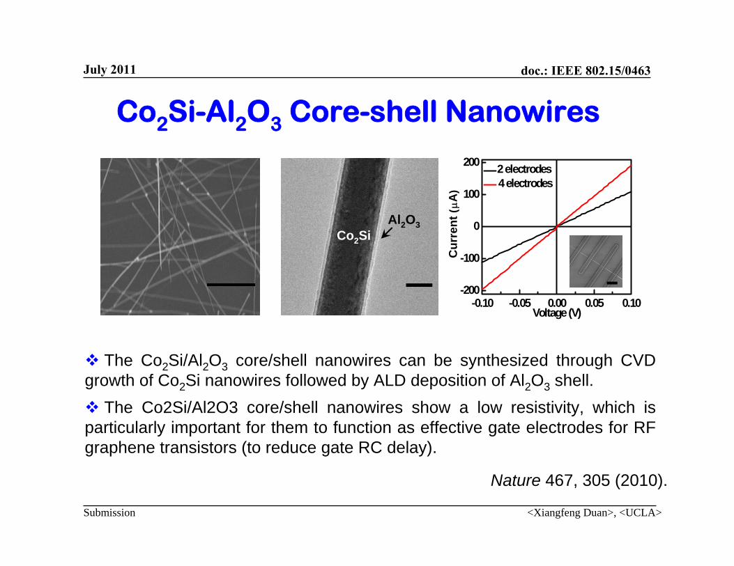
Co2Si-Al2O3 Core-shell Nanowires
The Co2Si/Al2O3 core/shell nanowires can be synthesized through CVD growth of Co2Si nanowires followed by ALD deposition of Al2O3 shell.
The Co2Si/Al2O3 core/shell nanowires show a low resistivity, which is particularly important for them to function as effective gate electrodes for RF graphene transistors (to reduce gate RC delay).
Nature 467, 305 (2010).
<Xiangfeng Duan>, <UCLA>
July 2011

doc.: IEEE 802.15/0463
Submission
High Performance Short Channel Graphene Transistors
-1.0 -0.5 0.0
-3
-2
-1
0
I ds
(mA
/μm
)
Vds (V)
2.0 V 1.6 V 1.2 V 0.8 V 0.4 V 0.0 V
-1 0 1 2 3
0.0
0.5
1.0
1.5 non self-aligned self-aligned
VTG (V)g m
(m
S/μm
)
-1 0 1 2 3
-0.46
-0.44
I ds (
mA
/μm
)
VTG (V)-1 0 1 2 3
-3.0
-2.5
-2.0
I ds
(mA
/μm
)
VTG (V)
1 m
Co2Si Pt
50 nm
The self-alignment allow a more 60 times improvement in trans-conductance to reach 1.27 ms/ m, promising ultrahigh speed transistors: fT = gm/(2πCg) ~323 GHz.
<Xiangfeng Duan>, <UCLA>
July 2011

doc.: IEEE 802.15/0463
Submission
Graphene Transistor with fT up to 300 GHz
On-chip microwave measurements demonstrate record high intrinsic cutoff frequency (fT) in the range of 100-300 GHz,.
The cutoff frequency of the graphene transistors is comparable to that of the very best high electron mobility transistors with similar gate lengths, marking an important milestone in graphene RF devices and can enable exciting opportunities in high-speed electronics.
100 101 102100
101
102
|h21
| Gai
n
Frequency (GHz)
L= 210 nmfT=125 GHz
100 101 102100
101
102
|h21
| Gai
n
Frequency (GHz)
L= 180 nmfT=168 GHz
100 101 102100
101
102
|h21
| Gai
n
Frequency (GHz)
1/f
L= 140 nmfT=300 GHz
Nature 467, 305 (2010).
<Xiangfeng Duan>, <UCLA>
July 2011
doc.: IEEE 802.15/0463
Submission
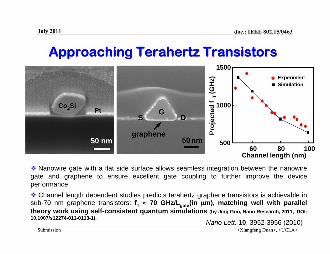
S DG
50nmgraphene
Co2SiPt
50 nm
Approaching Terahertz Transistors
Nanowire gate with a flat side surface allows seamless integration between the nanowiregate and graphene to ensure excellent gate coupling to further improve the deviceperformance.
Channel length dependent studies predicts terahertz graphene transistors is achievable in sub-70 nm graphene transistors: fT ≈ 70 GHz/Lgate(in m), matching well with parallel theory work using self-consistent quantum simulations (by Jing Guo, Nano Research, 2011, DOI: 10.1007/s12274-011-0113-1).
Nano Lett. 10, 3952-3956 (2010)
500
1000
1500
60 80 100Channel length (nm)
Proj
ecte
d f
T(G
Hz)
SimulationExperiment
<Xiangfeng Duan>, <UCLA>
July 2011

doc.: IEEE 802.15/0463
Submission
Towards Scalable Graphene Transistors
Large Area Graphene
Chemical vapor deposition and transfer of large area graphene
on variable substrate
Nature Nanotechnol. 5, 525 (2010)
High-yield self-limiting dielectrophoresis assembly of
single nanowires
Nanowire Gate Array
<Xiangfeng Duan>, <UCLA>
July 2011

doc.: IEEE 802.15/0463
Submission
Towards Scalable Graphene Transistors
pattern graphene
pattern E-field electrode
dielectrophoreticnanowireassembly
define source, drain and gate
electrodes
define self-aligned source and drain
electrodes
Nano Letters, 2011
<Xiangfeng Duan>, <UCLA>
July 2011

doc.: IEEE 802.15/0463
Submission
Towards Scalable Graphene Transistors
100 μm 5 μm50 μm
10-1 100 101 102100
101
102
103
Cur
rent
gai
n |h
21|
Frequency (GHz)-1 0 1 2 3 4
-1.2
-1.0
-0.8
I ds( m
A/μ m
)
VTG(V)-1.0 -0.5 0.0
-1.0
-0.5
0.0
I ds( m
A/ μm
)
Vds(V)
2.5 V2.0 V1.5 V1.0 V0.5 V0.0 V
-0.5 V
Nano Letters, 2011
<Xiangfeng Duan>, <UCLA>
July 2011
doc.: IEEE 802.15/0463
Submission
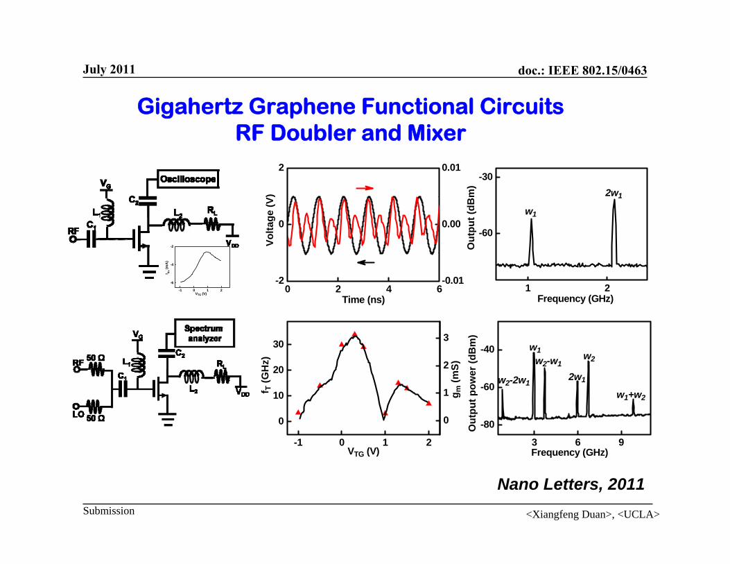
0 2 4 6-2
0
2
-0.01
0.00
0.01
Volta
ge (V
)
Time (ns)-1 0 1 2
-6
-4
-2
I ds (m
A)
VTG (V)1 2
-60
-302w1
Out
put (
dBm
)
Frequency (GHz)
w1
-1 0 1 2
0
10
20
30
0
1
2
3
g m (m
S)
f T (G
Hz)
VTG (V)
3 6 9
-80
-60
-40
w2-2w12w1
w2-w1
w1+w2
w2w1
Frequency (GHz)
Out
put p
ower
(dB
m)
Gigahertz Graphene Functional CircuitsRF Doubler and Mixer
Nano Letters, 2011<Xiangfeng Duan>, <UCLA>
July 2011

doc.: IEEE 802.15/0463
Submission
Graphene is emerging as an interesting material system for high speed electronics, but often require unconventional processes.
The physical assembly approach allows seamless integration of graphene with top-gate dielectrics without introducing any appreciable defects to preserve the high carrier mobility.
The self-aligned approach allows automatic and nearly perfect alignment of gate, source and drain electrodes, to enable short-channel graphene transistors with unprecedented speed.
The combination of CVD graphene and dielectrophoreticassembly allows scalable fabrication high speed graphenetransistors and circuits.
Summary
<Xiangfeng Duan>, <UCLA>
July 2011