İSTANBUL TECHNICAL UNIVERSITY INSTITUTE OF … · magnetic ballast test circuit ... göre ana...
97
İSTANBUL TECHNICAL UNIVERSITY INSTITUTE OF SCIENCE AND TECHNOLOGY M.Sc. Thesis by Orçun OTAR, B.Sc. Department : Electrical Engineering Programme: Electrical Engineering FEBRUARY 2007 AUTOMATIC LUMINOUS FLUX CONTROL FOR FLUORESCENT LAMPS
Transcript of İSTANBUL TECHNICAL UNIVERSITY INSTITUTE OF … · magnetic ballast test circuit ... göre ana...

İSTANBUL TECHNICAL UNIVERSITY INSTITUTE OF SCIENCE AND TECHNOLOGY
M.Sc. Thesis by
Orçun OTAR, B.Sc.
Department : Electrical Engineering
Programme: Electrical Engineering
FEBRUARY 2007
AUTOMATIC LUMINOUS FLUX CONTROL FOR FLUORESCENT LAMPS

İSTANBUL TECHNICAL UNIVERSITY INSTITUTE OF SCIENCE AND TECHNOLOGY
M.Sc. Thesis by
Orçun OTAR, B.Sc. 504041041
Date of submission : 25 December 2007
Date of defence examination: 29 January 2007
Supervisor (Chairman): Asst. Prof. Dr. Deniz YILDIRIM
Members of the Examining Committee Assoc. Prof. Dr. Dilek ENARUN
Asst. Prof. Dr. Metin AYDIN (KÜ.)
FEBRUARY 2007
AUTOMATIC LUMINOUS FLUX CONTROL FOR FLUORESCENT LAMPS

İSTANBUL TEKNİK ÜNİVERSİTESİ FEN BİLİMLERİ ENSTİTÜSÜ
T
Tez Dan
Diğer Jü
FLUORESAN LAMBALARDA OTOMATİK IŞIK AKISI KONTROLÜ
Y. LİSANS TEZİ Orçun OTAR
504041041
ezin Enstitüye Verildiği Tarih : 25 Aralık 2007Tezin Savunulduğu Tarih : 29 Ocak 2007ışmanı : Y.Doç.Dr. DenizYILDIRIM
ri Üyeleri Doç.Dr. Dilek ENARUN
Y.Doç.Dr. Metin AYDIN (KÜ.)
ŞUBAT 2007

ii
PREFACE
The aim of this project is to implement a daylight based controlled artifical lighting system and monitor the effects of these systems on energy consumption. However, the project cannot finished completely due to the restricted time period. Therefore, the project is focused on dimmable electronic ballast and fluorescent lamps. I hope the project will be continued and finished in the future.
First of all, I would like to thank my supervisor Asst. Prof. Dr. Deniz YILDIRIM for his valuable advice, support and encouragement to accomplish the project. Besides, I would like to thank Mr. Hikmet DURMAZ and Assoc. Prof. Dr. Dilek Enarun for their support in illumination laboratory. Special thanks to my family and friends Evren YÜCEL and Serdar BÖCEKÇİ who is always supported me.
February-2007 Orçun OTAR

iii
CONTENTS
PREFACE ii ABBREVIATIONS v LIST OF TABLES vi LIST OF FIGURES vii ÖZET ix SUMMARY x
1. INTRODUCTION 1 1.1. Introduction and Aim of Study 1
2. INTRODUCTION TO ELECTRIC LAMPS AND BALLASTS 4 2.1. Introduction to Lamps 4 2.1.1. The Conventional and The Compact Fluorescent Lamps 5
2.2. Introduction to Ballasts 7 2.2.1 The Magnetic Ballasts and The Electronic Ballasts 8 2.2.2 Resonant Half-Bridge Converter For Fluorescent Lamp Ballast 10 2.2.3 The Design Approach for The Ballast Output Stage 14 2.2.3.1 Sinusoidal Analysis of Resonant Converters 14 2.2.3.2 The Design Procedure of Ballast Output Stage 17 2.2.4 Dimming Operation of A Fluorescent Lamp 20 2.2.4.1 Dimming Control by Varying Duty-cycle 21 2.2.4.2 Dimming Control by Varying DC-link Voltage 21 2.2.4.3 Dimming Control by Varying Switching Frequency 22
3. EFFICIENCY IMPROVEMENT METHODS IN LIGHTING SYSTEMS 23 3.1 Introduction to Lighting Systems 23 3.2 Lighting Placement and Control Strategies 24
3.2.1 Local Task Lighting System 24 3.2.2 PSALI Lighting System 24 3.2.3 Localised Manual Switching Systems 25 3.2.4 Time-based Systems 25 3.2.5 Daylight-based Systems 25 3.2.6 Occupancy-based Systems 26 3.2.7 Lighting Management Systems 26
3.3 Control Parameters In Lighting Management Systems 27 3.3.1 Occupancy Sensors 27
3.3.1.1 Passive Infrared (PIR) Sensors 28 3.3.1.2 Ultrasonic Sensors 28 3.3.1.3 Acoustic Sensors 29
3.3.2 Photosensors 30 3.3.2.1 Photosensors for On-off Control 30

iv
3.3.2.2 Photosensor for Dimming Control 30 3.3.3 Dimming Ballasts 32
3.3.3.1 Analog Dimming Systems 32 3.3.3.2 Digital Dimming Systems 33
4. AUTOMATIC LUMINOUS FLUX CONTROL SYSTEM 36 4.1 Introduction 36
4.1.1 Sensor Section 39 4.1.2 Control Section 41 4.1.3 Power Section 41
4.2 Experiment Results of Ballast Test Circuits 43 4.2.1 Magnetic Ballast Test Circuit 43 4.2.2 Demonstration Ballast Test Circuit 45
5. CONCLUSION AND FUTURE WORKS 61
REFERENCES 62
APPENDICES 65
BIOGRAPHY 93

v
ABBREVIATIONS
AC : Alternative Current DC : Direct Current CFL : Compact Fluorenscent Lamp PFC : Power Factor Correction IC : Integrated Circuit PSALI : Permanent Supplementary Artificial Lighting System in Interiors LDR : Light Dependent Resistance PIR : Passive Infra Red DALI : Digitally Addressable Lighting Interface

vi
LIST OF TABLES
Page
Table 2.1 : Maximum lamp requirements for T8 fluorescent lamps..........….. 18 Table 2.2 Table 2.3 Table 4.1 Table 4.2 Table 4.3 Table 4.4
: Lamp operating variables for changing C values........................... : Design results for 32W/T8 fluorescent lamp…………................. : Characteristics of LDR samples…………..................................... : The measurement results of magnetic ballast test circuit.............. : The measurement results of ballast test circuit for utulity and lamp variables………………………………………………...….... : The measurement results of ballast test circuit for luminous flux change…………………………………………..………………....
19 20 40 43 49 56

vii
LIST OF FIGURES
Page
Figure 1.1 Figure 1.2 Figure 1.3 Figure 2.1 Figure 2.2 Figure 2.3 Figure 2.4 Figure 2.5 Figure 2.6 Figure 2.7 Figure 2.8 Figure 2.9 Figure 2.10 Figure 2.11 Figure 2.12 Figure 2.13 Figure 2.14 Figure 2.15 Figure 2.16 Figure 2.17 Figure 2.18 Figure 3.1 Figure 3.2 Figure 3.3 Figure 3.4 Figure 3.5 Figure 3.6 Figure 3.7 Figure 3.8 Figure 3.9 Figure 3.10 Figure 3.11 Figure 3.12
: Lighting consumption in all electric energy bills..................... : Lighting in office buildings electricity consumption............... : Electric illumination versus daylight in daylight based dimming systems……………………........................................ : Comparison of lamps excluding losses, in terms of lumens per watt...............……………………………………………… : Fluorescent lamp types......................................….................. : Conversion of electric energy into light in a fluorescent lamp : Power flow in: (a) an incandescent lamp (b) a fluorescent lamp…………………………………………………………… : Impedance – time characteristics of a fluorescent lamp.......... : Conventional ballast connection diagram.............................. : Ballast functional block diagram.................................……… : Simplified ballast output stage............................................…. : Simplified ballast diagram...................................................... : Self oscillating electronic ballast........................................…. : An IC based electronic ballast power(a) and driver(b) circuit. : Typical connection diagram of IR2153.................................. : Functional block diagram for IR2153.................................... : Half-bridge output voltage and its fundamental component.... : Equivalent circuit before ignition........................................... : Equivalent circuit after ignition........................................…. : Frequency response of ballast output stage (a) during ignition and (b) running……………………………….............. : Equivalent circuit of ballast output stage during running........ : PSALI method for placing luminaries..................................... : PSALI method with regular spacing........................................ : Trios Multisense Philips Lighting.............................…........... : Occupancy sensor control system............................................ : Typical coverage of passive infrared sensor............................ : Typical sensitivity pattern for wall-mount ultrasonic sensor... : A room with a photoelectric dimming system....................…. : Operation principle of an automatic light regulation system... : Typical 1-10V dimming system............................................... : Typical DALI dimming system............................…............... : DALI protocol bitstream definition......................................... : IRPLDIM2 Digitally Addressable Dimming Ballast………...
1 2 3 4 5 6 6 7 8 9 9 10 11 12 13 13 14 15 16 19 20 24 25 27 27 28 29 31 32 33 34 34 35
Figure 4.1 Figure 4.2
: The proposed system overview………………................…… : The block diagram of the proposed system…….................….
36 37

viii
Figure 4.3 Figure 4.4 Figure 4.5 Figure 4.6 Figure 4.7 Figure 4.8 Figure 4.9 Figure 4.10 Figure 4.11 Figure 4.12 Figure 4.13 Figure 4.14 Figure 4.15 Figure 4.16 Figure 4.17 Figure 4.18 Figure 4.19 Figure 4.20 Figure 4.21 Figure 4.22 Figure 4.23 Figure 4.24 Figure 4.25 Figure 4.26 Figure 4.27 Figure 4.28 Figure 4.29 Figure 4.30 Figure 4.31 Figure 4.32 Figure 4.33 Figure 4.34 Figure 4.35 Figure 4.36 Figure 4.37 Figure 4.38
: The overall circuit diagram of proposed system…….............. : Circuit diagram of light sensor................………………......... : Circuit diagram of control part................................................. : Circuit diagram of driver part.................................................. : Circuit diagram of ballast circuit..........................................… : Setup diagram of the magnetic ballast test circuit................... : Input voltage and current waveforms diagram of the magnetic ballast test circuit.................................……………... : Lamp voltage and current waveforms of the magnetic ballast test circuit................................................................................... : Setup diagram of the ballast test circuit for utility and lamp variables………………………………………………............. : Circuit diagram of the tested ballast circuit………....…......... : Frequency response of ballast output stage for L=1.37mH, C=2.5nF……………………………………...………....…....... : Gate signal waveforms of the upper and lower mosfets at 120kHz...............................................................................…… : Gate signal waveforms of the upper and lower mosfets at 70kHz.................................……………………….................... : Gate signal waveforms of the upper and lower mosfets at 50kHz..……………………....................................................... : Gate signal waveforms of the upper and lower mosfets at 30kHz..……………………....................................................... : Input voltage and current of the ballast at 30kHz.................... : Input voltage and current of the ballast at 50kHz.................... : Input voltage and current of the ballast at 70kHz...........……. : Input voltage and current of the ballast at 100kHz.…............. : Input voltage and current of the ballast at 121kHz.................. : Input voltage and current of the ballast at 132kHz. ................ : Voltage and current of the lamp at 30kHz............................... : Voltage and current of the lamp at 70kHz............................... : Voltage and current of the lamp at 100kHz.........................… : Voltage and current of the lamp at 120kHz............................. : Voltage and current of the lamp at 132kHz............................. : Setup diagram of the ballast test circuit for luminous flux...... : Frequency response of ballast output stage for L=1.37mH, C=10nF……………………………………...………....…........: Input voltage and current of the ballast at 49.93kHz............... : Input voltage and current of the ballast at 55.21kHz............... : Input voltage and current of the ballast at 58.12kHz............... : Input voltage and current of the ballast at 59.76kHz............... : Input voltage and current of the ballast at 61.00kHz…........... : Input voltage and current of the ballast at 62.12kHz............... : Input voltage and current of the ballast at 62.88kHz............... : Input voltage and current of the ballast at 63.44kHz...............
38 40 41 42 42 43 44 44 45 46 46 47 47 48 48 49 50 50 51 51 52 52 53 53 54 54 55 55 56 57 57 58 58 59 59 60

ix
FLUORESAN LAMBALARDA OTOMATİK IŞIK AKISI KONTROLÜ
ÖZET
Geçtiğimiz yıllarda, aydınlatma kontrol sistemleri, enerji tüketimiyle doğrudan ilişkili olduklarından enerjinin verimli kullanılması konusunda önemli bir rol oynamaktadır. Bu çalışmada, arttırılan verimlilik sayesinde enerji tüketimini azaltmayı mümkün kılabilecek, gün ışığı temelli dim edilebilen aydınlatma sistemleri önerilmektedir.
Önerilen sistemde, günışığının kullanılabilir olduğu zamanlarda, aydınlatma armatürlerinin ışık çıkışları azaltılarak enerji tüketimi düşürülebilmektedir. Dim edilebilen sistemde, foto sensörler aracılığıyla gün ışığı algılanır ve algılanan duruma göre ana kontrol merkezi sistem çıkışını, arzu edilen aydınlık düzeyine göre ayarlar. Tüm kontroller, kontrolde esneklik sağlayabilen programlanabilen mikrokontrolörler tarafından yapılmaktadır. Ayrıca, adreslenebilir radyo frekanslı seri haberleşme protokolü sisteme daha basit kurulum ve geniş esneklik sağlar.
Bu çalışma, fluoresan lamba ve balastlar hakkında temel bilgi, detaylı literatür ve piyasa araştırması, simülasyon, yapım ve deneysel gerçekleme bölümlerinden oluşmaktadır.

x
AUTOMATIC LUMINOUS FLUX CONTROL FOR FLUORESCENT LAMPS
SUMMARY
In recent years, artificial lighting control systems play an important role in energy saving topic that is directly related with energy consumptions. In this study, a daylight controlled dimming lighting system is proposed which enables to reduce energy consumption in terms of increased efficiency.
The proposed system provides to reduce the light output and energy consumption of lighting fixtures, whenever the daylight is available. In dimming system operation, photosensors sense the available daylight level and main controller of the system adjust, the light output to reach the desired lighting level. All control actions are performed by programmable microcontrollers that bring more flexibility in control operation. Moreover, an addressable RF wireless serial communication protocol is also employes in the system operation which provides simple installation and wide control flexibility.
The sections for this study includes a basic knowledge about fluorescent lamps and ballasts, a detailed literature and market search of existing systems, simulation, construction and experimental verification.

1
1. INTRODUCTION
1.1 Introduction and Aim of Study
After the world had faced with the first energy crisis caused by unexpected rise in oil price during 1970’s, people in electric industry tend to search new alternative ways for meeting the world’s increasing energy demand. Firstly, people decided to make investments and use non-conventional energy sources such as wind, solar, wave, etc. However, by the nineties this idea become weaker against an another idea that the energy demand could be limited or reduced by saving energy in terms of efficiency [1]. According to that, the investments in conservation of energy like using suitable and efficient technology in each utility are more effective than the investments in power plants. Moreover, a reduction in energy consumption means saving money and reduction in pollution.
Electric lamps and artificial lighting are related with this conservation of energy and also they have important place in energy consumption. For instance, in the United States lighting consumes nearly 20 percent of all electricity consumption as shown in Figure 1.1 and also Figure 1.2 shows that lighting loads has a significant place in commercial buildings electricity usage.
Figure 1.1 : Consumption of lighting in all electric energy bills. (Energy Star Inc. Buildings Manual).

2
Figure 1.2 : Lighting in office buildings electricity consumption. (Energy Star Inc. Buildings Manual).
Since, using lighting efficiently is an important case in energy efficiency, the most common lighting source, fluorescent lamps are in the middle of energy efficiency. The gas discharge lamps have been known over fifty years and most of the efficient lighting projects focused on the fluorescent lamp technology in terms of low-wattage lamps and high efficient electronic ballasts.
Among the efficient lighting systems, the dimming systems have a significant importance. The fluorescent dimming occurs in the ballast and dimming ballast is the hearth of the dimming system. The aim of dimming control is to reduce the output and energy consumption of lighting fixtures when the available daylight gives sufficient light. In dimming systems, photosensors measure the available natural daylight and main controller adjusts the lighting system output to reach the required lighting level. Figure 1.3 illustrates the main idea of the daylight based dimming systems.

3
Figure 1.3 : Electric illumination versus daylight in daylight based dimming systems (Washington State University Energy Program Fact-sheet).
There are a lot of studies focused on dimmable systems to develop and make them more efficient. However, there is surprisingly a little reliable information about energy savings of these dimmable systems. A study titled “Fifty percent energy savings with automatic lighting controls” made in an office building in San Francisco during nine month operation shows that more than fifty percent of energy savings relative to previous usage is achieved with applied system [3]. Another study made in Philip Barton Federal Building in San Francisco resulted that occupant sensors saved 18 – 24 % of lighting energy compared to manual switching, and in offices where the light sensors are installed an additional savings of up to 20 % is obtained [4]. Moreover, a daylight control system applied in The New York Times Headquarters Building has an average of 20 – 23 % of energy savings [5, 6].
The aim of this study is to develop and construct a daylight controlled lighting system. The methods for this study includes basic knowledge about lighting and gas discharge lamps, a detailed literature and market survey of existing systems, simulation, construction and experimental validation of the concept.

4
2. INTRODUCTION TO ELECTRIC LAMPS AND BALLASTS
2.1 Introduction to Lamps
The energy saving lamps phrase becomes a synonym with the developing fluorescent lighting technology. In fact, the popular term of energy saving lamps is a new term for the fluorescent lamps that appears with the new developments in the fluorescent lamp technology. Today, the lighting industry is interested in the new technologies such that low-wattage fluorescent lamps and highly efficient electronic ballasts.
Lamps can be different from each other in terms of their luminous efficiency and in terms of lumens per watt as shown in Figure 2.1. Lamps and efficiency are related with this conversion of energy. Today’s most popular electric lamp for providing illumination is the incandescent lamps. Despite the least light output for a given amount of energy, the incandescent lamps have been used over a century.
The other most popular source of lighting is fluorescent lamp. Its working principle is based on an electric arc discharge through a gas at a low pressure. This principle is known for years and also many researches and developments are made to improve their luminous efficiency. Generally, the fluorescent lamps have a good efficiency of about 90 lumen/watt excluding the power losses in the ballast. Efficiency drops to about 75 lumen/watt with the losses in ballast, which is far better than incandescent lamp efficiency about 20 lumen/watt [1].
Figure 2.1 : Comparison of lamps excluding losses, in terms of lumens per watt [1].

5
Nowadays, the fluorescent lamps are commonly used in every area of life as a source of light. Fluorescent lamps are popular, because they provide longer lifetime and consume less energy than incandescent lamps. Moreover, their low intensity illumination is preferred in almost all indoor applications. The high intensity discharge lamps such as mercury or sodium vapor lamps are used primarily in outdoor environment to illuminate large areas such as streets, parks, etc. [2].
2.1.1 The Conventional and The Compact Fluorescent Lamps
In conventional means, a fluorescent lamp is a tube which is covered with a fluorescent powder from the inside. A mercury vapor at low pressure with a small amount of inert is also added gas to help ignition. The two electrodes are placed at the ends of the lamp and are separated from each other by their operating conditions such as “cold” or “hot” [1,2].
Figure 2.2 : Fluorescent lamp types.
Cold and hot terms are resulted from how the lamp is designed to operate in a such way either hot or cold temperatures. The coated tungsten electrodes have high operating temperatures, so these kinds of lamps are called “hot cathode” lamps. The coated iron or nickel electrodes have low temperatures conditions, so these kinds of lamps are called “cold-cathode” lamps. In hot-cathode lamps the voltage drop at the electrodes is low (10V) due to the heated cathodes. In cold-cathode lamps the voltage drop across the electrodes are high (50V) due to the low temperatures, and this results in a longer life.
In operating conditions, everything starts with an electric arc between the two electrodes. The effect of meeting of these electrons with the mercury vapor creates ultraviolet radiation which are partially seen. The main task of making these radiations visible is done by the fluorescence coating of the lamp. Figure 2.3 shows

6
the energy conversion in a fluorescent lamp. The color of the light is given by this chemical composition and can be changed and be also improved by changing the composition [1,2].
Figure 2.3 : Conversion of electric energy into light in a fluorescent lamp [2].
Typical power flow of a standard 40 watt fluorescent lamp results in 60% of the energy being converted to discharge radiation, i.e., approximately 24 watts. However, only 20% of this radiation or 8 watts is transformed into light. The remaining 40% of the UV energy and a total of 78% of the total energy used by the lamp is transformed into heat and infrared radiation. Only 22% of the total lamp wattage is actually transformed into visible radiation or light. Both the incandescent lamp and the fluorescent lamp power flow are shown in Figure 2.4 [8].
Figure 2.4 : Power flow in: (a) an incandescent lamp (b) a fluorescent lamp [8].
However, the conventional fluorescent lamps lost their popularity as the compact fluorescent lamps (CFL) have come to the market. The CFL has a wide application area that the conventional one can be used such as in homes. Moreover, the conventional lamps have some disadvantages such as the need of an external ballast, emitting audible noise and blinking. But, the CFL can directly be replaced with the incandescent one and there is also no need of any external component. Beside all the advantages of CFL, they are not suitable to use in dimmable systems.

7
2.2 Introduction to Ballasts
Due to decreasing impedance characteristic, a fluorescent lamp cannot directly be connected to the line voltage. Therefore, a device called ballast that is adjusts the voltage and current of the lamp becomes a necessity. The function of ballast can be described into two main parts.
A high ignition voltage between the two electrodes during starting is an important function of ballast. The other one is the need of limiting the current to protect the lamp from the overcurrents during normal operation. These relations can be seen in change of impedance as a function of time for a gas discharge lamp as seen in Figure 2.5 [1, 2].
Figure 2.5 : Impedance – time characteristics of a fluorescent lamp [1].
As easily seen from the Figure 2.5, at first, the value of the impedance is high. Therefore, a higher voltage than the normal operating, conditions must be applied to ignite the arc. After the ignition, the impedance value drops to a minimum. While impedance value is decreasing, the current value is increasing. Therefore, current must be limited at a level which protects the lamp from overcurrents [1,2].
These two requirements are expected from a conventional magnetic ballast. However, today’s new developed electronic ballasts can fulfill these requirements as well as many other functions like dimming, power factor correction (PFC) etc. In fact, the fluorescent lamp is a resistive load, but the addition of ballast (magnetic or electronic) results in some problems such as harmonics and low power factor. Therefore, the IC manufacturers made researches about developing the ballast technology and solving the existing problems [8, 9].

8
2.2.1 The Magnetic Ballasts and The Electronic Ballasts
In conventional magnetic ballast connection as shown in Figure 2.6, the lamp requirements are met by ballast and a thermal switch. The magnetic ballast is an inductor where a certain number of turn coils are wound around a magnetic core. These types of ballasts dissipate about the 20 percent of the total power drawn lamp. Moreover, it has a low power factor. The other disadvantages of conventional ballasts are blinking, stroboscopic effect due to the 50 Hz frequency and difficulty of dimming [1, 8].
Figure 2.6 : Conventional ballast connection diagram [1].
Although the magnetic ballasts are still used today, the electronic ballasts are commonly preferred to be used due to their superiority. Moreover, the problems that occur with the use of magnetic ballasts can be solved by using electronic ballast. For instance, blinking problem does not occur due to the high frequency operation. The electronic ballast technology is developed in recent years and dedicated the integrated circuits are preferred to use in electronic ballasts instead of complex circuits employing many discrete component.

9
Figure 2.7 : Ballast functional block diagram [9].
Today’s electronic ballasts must satisfy some functions like eliminating ballast generated noise with EMI filtering, rectification, having a sinusoidal input current with power factor correction (unity power factor), having half-bridge switches with driver for high frequency operation and powering the lamp with the output stage as shown in Figure 2.7 [9].
Figure 2.8 : Simplified ballast output stage [9].
In the electronic ballast, the main part of the job is done by the output stage that consists of a high frequency half-bridge driver (Vin), a series inductor (L) with a parallel capacitor (C) and lamp (R). In this connection the lamp requirements such as a current for a specified time to preheat the filaments, a high voltage for ignition and running power can be provided by supplying the proper frequency and magnitude of the input voltage Vin and selecting L and C values [9, 11, 19, 20].

10
2.2.2 Resonant Half-bridge Converter for Fluorescent Lamp Ballast
Voltage-fed series resonant half-bridge inverters are used in currently for fluorescent lamp ballasts. This topology allows switches operating in zero-voltage resonant mode, reducing the transistor switching losses and the electromagnetic interference.
Electronic ballast circuits have recently been developed by the advent of the mosfet switches. Most electronic ballasts include two power switches (S1, S2) in half-bridge configuration and an L-C series resonant circuit with the lamp as illustrated in Figure 2.9. By varying the switching frequency and properly selecting Vin, L and C, it is possible to adjust required current and the voltage values [9, 11, 19, 20].
Figure 2.9 : Simplified ballast diagram [11].
The main purpose of the switching operation is to drive the Lres-Cres circuit at their resonant frequency. Therefore, driving the mosfet switches becomes the most important part of the electronic ballast operation. The two mosfet switches S1 and S2 are switched to obtain a high frequency rectangular ac voltage across the resonant L-C circuit. The dc blocking capacitor Cb eliminates the dc voltage component. The resonant voltage across the resonant capacitor Cres causes arc across the lamp electrodes to strike. The drive operation can be realized in many ways in which some of them are explained here.
A self oscillating electronic ballast is illustrated in Figure 2.10. The switches in the circuit below are the power mosfets driven to conduct alternatively by two secondary windings on a transformer. The primary of this transformer is driven by the current in the lamp circuit operating at the resonant frequency of LR and CR. The circuit is not self starting and must be pulsed started by a Diac connected to the gate of the lower mosfet. After the lower mosfet is turned on, oscillation is sustained and a high

11
frequency square wave excites the LR-CR resonant circuit. The sinusoidal voltage across CR is magnified by the quality factor at resonance and develops required value to strike the lamp. The operating frequency is determined by the parallel combination of R-C circuit connected to the diac [1].
Figure 2.10 : Self oscillating electronic ballast [1].
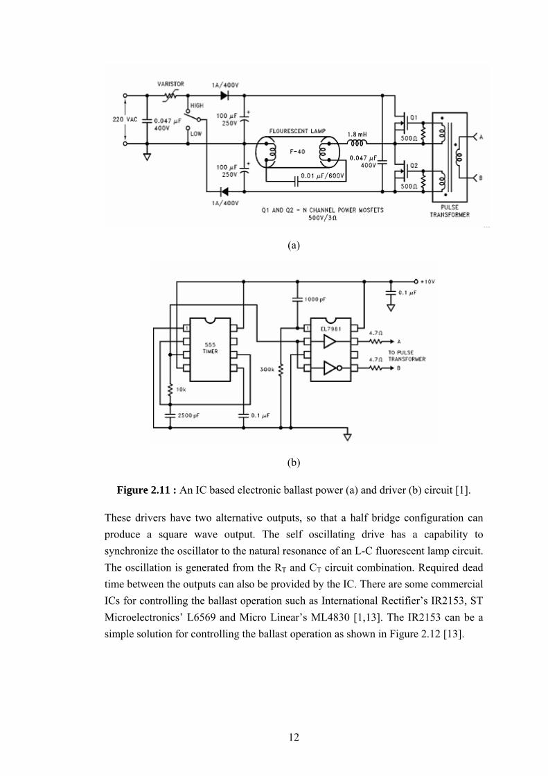
In the second circuit as shown in Figure 2.11, the operating voltage can be changed with a switch. First, in the line is rectified and doubled or the doubler can be eliminated when the switch is low position. Then, a half bridge by using Mosfets drive an LR-CR resonant circuit.
The desired clock frequency is generated by a 555 timer and also the clock can be tuned on the resonant frequency of the series LR (1.8mH) -CR (10nF) by changing the R (10k) and C (2500pF). Moreover, the driver IC generates the pulses to the transformer with a required dead time between the complimentary outputs [1].
Since the size and the cost are two important factors in designing ballast circuits, the IC manufacturers developed dedicated ICs that can produced the required gate drive signals with a few extra components. The self oscillating half bridge drivers are designed to control the ballast in terms of dimming or power factor controlling.
12
(a)
(b)
Figure 2.11 : An IC based electronic ballast power (a) and driver (b) circuit [1].
These drivers have two alternative outputs, so that a half bridge configuration can produce a square wave output. The self oscillating drive has a capability to synchronize the oscillator to the natural resonance of an L-C fluorescent lamp circuit. The oscillation is generated from the RT and CT circuit combination. Required dead time between the outputs can also be provided by the IC. There are some commercial ICs for controlling the ballast operation such as International Rectifier’s IR2153, ST Microelectronics’ L6569 and Micro Linear’s ML4830 [1,13]. The IR2153 can be a simple solution for controlling the ballast operation as shown in Figure 2.12 [13].

13
Figure 2.12 : Typical connection diagram of IR2153 [13].
The IC includes a timer circuit integrated with a half bridge driver and also the running frequency can be programmed with a resistor and a capacitor. A functional block diagram of IR2153 is shown in Figure 2.13.
Figure 2.13 : Functional block diagram for IR2153 [13].
Moreover, other additional ballast functions like programmable operating frequency, circuit and lamp protection and dimming can be made by ICs. There are a lot of available ICs in International Rectifier family such as IR2155, IR2157 or a dimming version IR2159.
14
2.2.3 The Design Approach for The Ballast Output Stage
The focus of this section is on analysis and design of the output stage using a simplified circuit model. During preheat and ignition conditions, since the lamp has an infinite resistance, the lamp is not conducting and the resulting circuit is a series L-C circuit. For running condition, the lamp is conducting due to decreasing lamp resistance and the circuit becomes an inductor (L) in series with a parallel R-C.
The magnitude of the transfer function (lamp voltage divided by the input voltage) for the two circuit configurations, illustrates the operating characteristics for the design approach such as the maximum current and voltage ratings for the inductor, capacitor and the switches etc. [9, 13, 19].
2.2.3.1 Sinusoidal Analysis of Resonant Converters
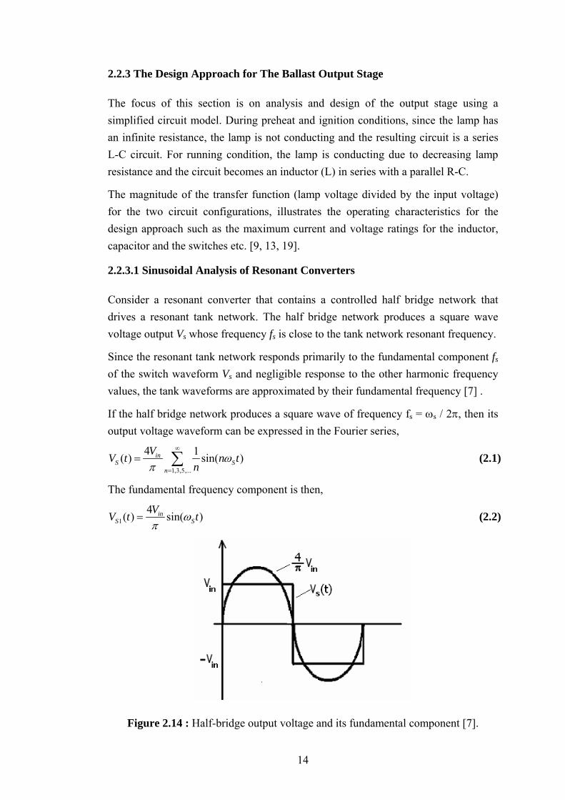
Consider a resonant converter that contains a controlled half bridge network that drives a resonant tank network. The half bridge network produces a square wave voltage output Vs whose frequency fs is close to the tank network resonant frequency.
Since the resonant tank network responds primarily to the fundamental component fs of the switch waveform Vs and negligible response to the other harmonic frequency values, the tank waveforms are approximated by their fundamental frequency [7] .
If the half bridge network produces a square wave of frequency fs = ωs / 2π, then its output voltage waveform can be expressed in the Fourier series,
1,3,5,...
4 1( ) sin( )inS S
n
VV t n tn
ωπ
∞
=
= ∑ (2.1)
The fundamental frequency component is then,
14( ) sin( )in
S SVV t tωπ
= (2.2)
Figure 2.14 : Half-bridge output voltage and its fundamental component [7].
15
This analysis uses the fundamental frequency component of the square-wave voltage produced the half bridge switches and other harmonics are assumed negligible [9, 11, 19].
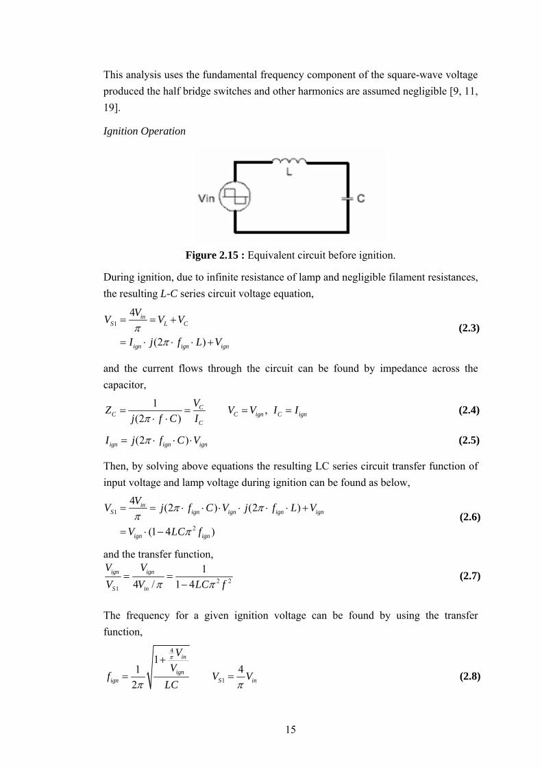
Ignition Operation
Figure 2.15 : Equivalent circuit before ignition.
During ignition, due to infinite resistance of lamp and negligible filament resistances, the resulting L-C series circuit voltage equation,
14
(2 )
inS L C
ign ign ign
VV V V
I j f L Vπ
π
= = +
= ⋅ ⋅ ⋅ + (2.3)
and the current flows through the circuit can be found by impedance across the capacitor,
1 ,(2 )
CC C ign C ign
C
VZ V V I Ij f C Iπ
= = = =⋅ ⋅
(2.4)
(2 )ign ign ignI j f C Vπ= ⋅ ⋅ ⋅ (2.5)
Then, by solving above equations the resulting LC series circuit transfer function of input voltage and lamp voltage during ignition can be found as below,
1
2
4 (2 ) (2 )
(1 4 )
inS ign ign ign ign
ign ign
VV j f C V j f L V
V LC f
π ππ
π
= = ⋅ ⋅ ⋅ ⋅ ⋅ ⋅ +
= ⋅ − (2.6)
and the transfer function,
2 21
14 / 1 4
ign ign
S in
V VV V LC fπ π
= =−
(2.7)
The frequency for a given ignition voltage can be found by using the transfer function,
4
1
11 4
2
in
ignign S in
VV
f V VLC
π
π π
+= = (2.8)

16
The associated ignition current flowing in the circuit that determines the maximum current ratings for L and half-bridge switches can be found by again using the impedance across the capacitor such as,
2ign ign ignI f C V π= ⋅ ⋅ ⋅ (2.9)
where, Vin = Input square-wave voltage amplitude [volts]
Vign = Lamp ignition voltage amplitude [volts]
Iign = Lamp ignition current amplitude [amps]
fign = Lamp ignition frequency [Hz]
L = Output stage inductors [henries]
C = Output stage capacitor [farads]
Running Operation
Figure 2.16 : Equivalent circuit after ignition.
Once the lamp is ignited, the resistance of the lamp is no longer negligible, and the system becomes a low quality factor RCL series-parallel circuit voltage equation,
14
( )
inS L C
run run
VV V V
I j L Vπ
ω
= = +
= ⋅ ⋅ + (2.10)
and the current flows through the circuit is row sum of the lamp and capacitor currents,
( )
1 ( )
run R C
runrun
run
I I IV V j CR
j C VR
ω
ω
= +
= + ⋅ ⋅
⎡ ⎤= + ⋅ ⋅⎢ ⎥⎣ ⎦
(2.11)
17
Then, by combining equation 2.10 and 2.11, the resulting RCL series-parallel circuit transfer function of input voltage and lamp voltage during running can be found as below,
1
2
4 1[ ( )] ( )
( )[1 ]
inS run run run run
runrun run
VV j C V j L VR
j LV L CR
ω ωπ
ωω
= = + ⋅ ⋅ ⋅ ⋅ +
⋅= ⋅ − ⋅ ⋅ +
(2.12)
and the transfer function,
21 2 2 2
2
14 /
(1 )
run run
S inrun run
V VV V LLC
Rπ
ω ω= =
− +
(2.13)
The running frequency becomes,
2
2
12 2 2 2 2 2
411 1 1 1 1 4
2 2 2
in
runrun S in
VV
f V VLC R C LC R C L C
ππ π
⎛ ⎞− ⎜ ⎟
⎡ ⎤ ⎝ ⎠= − + − − =⎢ ⎥⎣ ⎦ (2.14)
where R is assumed to be the linearized lamp resistance determined from the running lamp power and voltage at a single operating point,
2 2
r r
1P 2 P2
run run
un un
V VR ⎛ ⎞= ⋅ =⎜ ⎟⎝ ⎠
(2.15)
where,
Vin = Input square-wave voltage amplitude [volts]
Prun = Lamp running power [watts]
Vrun = Lamp running voltage amplitude [volts]
Irun = Lamp running current amplitude [volts]
frun = Lamp running frequency [Hz]
2.2.3.2 The Design Procedure of Ballast Output Stage
Designing an efficient ballast output stage is based on considering the lamp requirements. The first step is therefore, to determine the manufacturer’s recommended lamp power, running voltage and ignition voltage values. The lamp requirements for T8 lamps are given in Table 2.1 [IR Ballast Design Software].

18
Table 2.1 : Maximum lamp requirements for T8 fluorescent lamps.
The second step is to calculate an inductance (L) value based on the power in the lamp during running. For an optimum transfer of energy to the low-Q RCL circuit, half of the input voltage will be across L, where the output stage input power is :
1 4 4 ( )22 2 2
S in in in runin in in
run
V V V V PP I ILω ηπ π
= = = = (2.16)
The output stage efficiency, η, takes into account switching and conduction losses in the half bridge switches and losses in inductor and the filaments. Solving for L as a function of lamp power yields [9]:
2
22in
run run
VLf P
ηπ
= (2.17)
For a T8/32W fluorescent lamp, the lamp requirements are determined to be :
Vign = 550 Volts
Prun = 32 Watts
Vrun = 141 Volts
Selecting a reasonable running frequency of about 35kHz, assuming an efficiency of 95%, and setting the DC bus to 300VDC for universal input (Vin=150V), gives an inductor value of 1.37 mH for a lamp power of 32W. How well this value for L depends on the selecting the C and how well the other operating conditions are fulfilled.
The formulas that are derived in the previous part can be used to select the correct C values. As shown in Table 2.2, for a number of C values from 1nF to 10nF the equations are calculated and also 10nF gives the most suitable result among them since the calculated frequency values and the selected frequency values are more close to each other. In fact, the best result can be obtain with using iterative methods.

19
Table 2.2 : Lamp operating variables for changing C values.
Moreover, the frequency response of the ballast output stage or lamp’s ignition (A) and running (B) voltage changes according to the input voltage are illustrated in Figure 2.17. The ballast output stage plotted in figure includes a 1.37mH inductor, a 10nF capacitor and a 300Ω lamp resistor during running.
Figure 2.17 : Frequency response of ballast output stage (a) during ignition and (b) running.
The next stage is determining the maximum current ratings of the inductance and the switches. From the equation 2.9, the ignition current is found nearly 1 amp. Moreover, the running current can be found from the running voltage and power. These current ratings will be needed while designing the inductance.

20
Since the DC bus voltage is nearly 300 VDC, we need to eliminate the DC component of bus voltage. The series capacitor, Cse makes this and then, the Vin becomes 150 V. The value of the series capacitor is selected 100nF according to reference designs. The design results for 32W/T8 lamps can be seen in Table 2.3 below.
Table 2.3 : Design results for 32W/T8 fluorescent lamp.
2.2.4 Dimming Operation of A Fluorescent Lamp
Modern electronic ballasts require some added features such as, high-frequency preheats for filaments, nominal lamp-power control, and light-dimming capability. The dimming operation of a fluorescent lamp is directly related to control the lamp power [10].
Figure 2.18 : Equivalent circuit of ballast output stage during running [10].
The impedance of the ballast resonant tank equivalent circuit shown in above Figure 2.18 is
2
1lamp r r lamp r
eqr lamp
R L C R j LZ
j C Rω ω
ω− +
=+
(2.18)

21
Assuming lamp voltage does not change significantly, the lamp power i.e., luminous flux can be controlled by the lamp current, which can be expressed as:
in Lrlamp Lr Cr
lamp
V VI I IR−
= − = (2.19)
The ac voltage Vin is varied by DC link voltage of the inverter and also the lamp resistance Rlamp is increased during reducing power. In fact, fluorescent lamps are usually designed for operating in unique definite conditions due to discharge lamp’s non-linear and negative incremental impedance characteristic. Moreover, the lamp becomes unstable at low power levels. Therefore, some problems can be occurred in dimming operations such as flickering or extinguish. In practical manner, controlling the lamp current can be achieved in three ways as described below [10].
2.2.4.1 Dimming Control by Varying Duty-cycle
In order to change the lamp power in a ballast circuit, simply the duty cycle of the half-bridge switches can be controlled. The duty cycle can be adjusted between 0 to 50%. However, a very small duty cycle can result in a discontinuous inductor current and as a result zero voltage switching conditions will be lost resulting in high switching losses.
Moreover, this discontinuous current operation increases the EMI emission. The duty cycle control yields a restricted dimming range of a fluorescent lamp. Because of these problems, duty cycle control is not a preferable method in electronic ballast dimming [10].
2.2.4.2 Dimming Control by Varying DC-link Voltage
Another method to control lamp power is controlling the input DC voltage of the half bridge switches. The duty cycle of the half bridge switches remains constant nearly 50% to obtain a continuous inductor current for soft switching operation.
Since, the operating frequency is constant during operation, EMI filter design and switching control become very simple. Moreover, due to zero voltage switching under constant frequency condition, the L-C resonant tank with half bridge circuit parameters can be easily determined.
As shown in the lamp current equation 2.11, the magnitude of the high frequency AC voltage which is formed by the half bridge inverter’s DC input voltage is directly proportional to the magnitude of the lamp current [10, 22].
lamp DCI Vα (2.20)

22
2.2.4.3 Dimming Control by Varying Switching Frequency
The most common commercial dimming control method is the frequency control. Since, the output inverter operates in resonant mode, we can control the power or current of these ballasts simply by varying the switching frequency.
The variable frequency results in a change in the impedance values for the resonant tank elements. As the frequency ωS increases, the impedance of the inductor increases whereas the impedance of the capacitor decreases. In addition, the lamp resistance Rlamp has an increasing characteristic with reducing lamp power. These impedance changes affect the lamp current in two ways:
• Firstly, the higher the frequency, the higher the impedance of the inductor. This will decrease the current to the lamp. The lower the frequency, the lower impedance of the inductor, and this will increase the current to the lamp.
• Secondly, an increase in the operating frequency causes that a decrease in capacitor impedance and an increase in lamp resistance. This means the current flow from the lamp branch will reduce and diverted to the capacitor due to increasing lamp branch impedance. According to two effects, the operating frequency and the lamp current is inversely proportional to each other.
1 lampS
I αω
(2.21)
In frequency base of dimming control, controlling the lamp the power needs a very wide frequency range about 25 to 120 kHz. Therefore, during design process of magnetic cores and electronic circuits, wide frequency changes have to be considered [10, 11].

23
3. EFFICIENCY IMPROVEMENT METHODS IN LIGHTING SYSTEMS
3.1 Introduction to Lighting Systems
In recent years, many technological developments about lighting industry had been occurred. In lamp and electronic ballast technology there have been new developments resulting higher efficiencies and longer lifetimes. Improvements in electronic ballasts technology in fluorescent lamps provide non-flicker operation, longer lifetime, faster start-up, cooler operation and providing smooth and silent dimming ability. Moreover, developments in electronic controls for lighting such as daylight based control or occupancy based control becomes popular in daily life.
All of these technological developments in the lighting industry have resulted in improvements in lighting efficiency, and thus a reduction in energy consumption and cost. In many studies focused on this subject showed that electricity consumption can be reduced by 65% or more and payback time for the cost of the lighting fixture upgrade is typically between one to three years. In addition, developments in lighting improve the quality of light emanating from the lamp.
Improvements in lighting efficiency can be provided in some different arrangements in lighting equipments and lighting design. For instance, replacing low efficient lamps i.e., incandescent lamps with more efficient lamps, replacing standard ballasts with high frequency electronic ballasts or replacing standard luminaries with high efficiency luminaries can be arrangements in terms of lighting equipment.
Another arrangement can be made in lighting design such as localized switching to control local lighting, maintenance lighting fixtures regularly and local task lighting to reduce overhead lighting. At this point, the Permanent Supplementary Artificial Lighting in Interiors systems (PSALI) that maximize the use of daylight have been used for years in designing the lighting systems [12].
Moreover, the more complicated arrangement is the use of automatic control systems in lighting design. These systems are based on timer circuits, occupancy or photoelectric sensors. Both timer circuits and occupancy sensor, based system turns off lamps during vacancy times or unoccupied times in workstations. However, in the photoelectric sensors based control systems, the amount of daylight in the room is sensed and the lamp brightness is controlled accordingly [12].

24
3.2 Lighting Placement and Control Strategies
3.2.1 Local Task Lighting System
This method for reducing energy comprises designing both task and ambient lighting separate from each other. For instance, the overhead lighting obtains overall illumination and is kept at a certain value, while the desired task lighting is obtained in the local areas. By using this approach, less energy is consumed than overhead illumination and also a variable lighting can be provided in workplace [12, 24].
3.2.2 PSALI Lighting System
Another approach in lighting design is PSALI developed by Hopkinson and Longmore in 1959’s. In conventional systems, luminaries are designed to be placed in the ceiling in a symmetrical manner [12].
Figure 3.1 : PSALI method for placing luminaries [12].
However, in PSALI system more luminaries are placed far away from the window zones and fewer luminaries near window zones, which obtains more balanced lighting in spaces (Figure 3.1). When the daylight level is bright enough to maintain sufficient lighting level, only row C is turned on. When the daylight level decreases below to certain level, row B needs to be turned on in place of row B. At dark days and nights, it would be necessary to turned on all rows except row C [12].
25
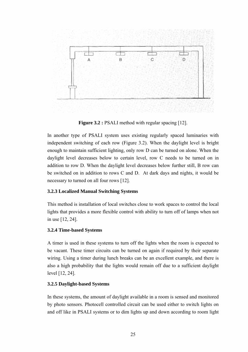
Figure 3.2 : PSALI method with regular spacing [12].
In another type of PSALI system uses existing regularly spaced luminaries with independent switching of each row (Figure 3.2). When the daylight level is bright enough to maintain sufficient lighting, only row D can be turned on alone. When the daylight level decreases below to certain level, row C needs to be turned on in addition to row D. When the daylight level decreases below further still, B row can be switched on in addition to rows C and D. At dark days and nights, it would be necessary to turned on all four rows [12].
3.2.3 Localized Manual Switching Systems
This method is installation of local switches close to work spaces to control the local lights that provides a more flexible control with ability to turn off of lamps when not in use [12, 24].
3.2.4 Time-based Systems
A timer is used in these systems to turn off the lights when the room is expected to be vacant. These timer circuits can be turned on again if required by their separate wiring. Using a timer during lunch breaks can be an excellent example, and there is also a high probability that the lights would remain off due to a sufficient daylight level [12, 24].
3.2.5 Daylight-based Systems
In these systems, the amount of daylight available in a room is sensed and monitored by photo sensors. Photocell controlled circuit can be used either to switch lights on and off like in PSALI systems or to dim lights up and down according to room light

26
level. By the advent of high frequency ballasts, fluorescent lamps can be able to be dimmed to a very low level with flicker-free operation [12].
3.2.6 Occupancy-based Systems
The heart of these systems is occupancy sensors that are responsible to switch lights off when the room is unoccupied. There are several different types of sensors available such as infra-red, ultra-sonic, acoustic, and thermal or microwave, which sense movement, temperature or noise. Moreover, a time delay is needed in these systems to avoid wrong detections during operation [12, 24].
3.2.7 Lighting Management Systems
In recent years there have been huge developments in the area of lighting management systems by use of microcontrollers. In these systems, sensors are installed to monitor either daylight level or occupancy status or both. In addition, a lamp or groups of lamps can be dimmed or switched off according to desired situation. Due to ability to combine both daylight-based and occupancy-based controls, the efficiency of the lighting system can be maximized.
The commercial examples of lighting management systems are available in the market manufactured by lighting firms such as Philips Lighting and WILA.
A German firm WILA introduced a light management system for remote control at the Hanover Light Fair in 1997. The system called “E Control Scenario” is a daylight-based system, but occupancy sensors can also be added. In this system, a group of luminaries can be controlled by manually or by the sensor information, and also luminaries can be programmed for different scenarios. In addition, the system can be linked to a computer for monitoring and controlling of the overall system [12].
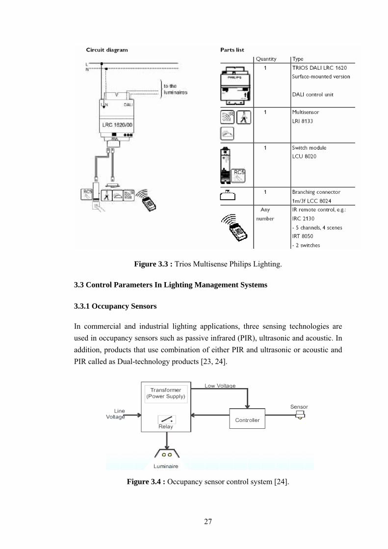
The other commercial lighting management system that was first introduced in 1996 by Philips Lighting is called “Trios Multisense” system with sensors that monitor daylight level and occupancy status. The system is designed to be installed into a luminary and can control a group of lighting fixture containing 64 electronic ballasts. Moreover, Trios has five preset programs which can be activated by infra-red remote control [12].
27
Figure 3.3 : Trios Multisense Philips Lighting.
3.3 Control Parameters In Lighting Management Systems
3.3.1 Occupancy Sensors
In commercial and industrial lighting applications, three sensing technologies are used in occupancy sensors such as passive infrared (PIR), ultrasonic and acoustic. In addition, products that use combination of either PIR and ultrasonic or acoustic and PIR called as Dual-technology products [23, 24].
Figure 3.4 : Occupancy sensor control system [24].

28
3.3.1.1 Passive Infrared (PIR) Sensors
PIR sensors react to movement of infrared sources like human bodies in motion. PIR sensors have a pyroelectric detector that is sensitive to the infrared radiation emitted by objects at a temperature around human body and also an IR transmitting lens with view segments is placed in front of the pyroelectric detector. The range and sensitivity of a PIR sensor is greatly related with the type of lens used. Different lens types are available for different applications. For instance, an overall wide field of view with narrow view segments are used for room occupancy sensors, while an overall narrow field of view with larger view segments are used for corridors [23, 24].
Figure 3.5 : Typical coverage of passive infrared sensor [24].
Due to consuming very little energy, PIR sensors have a potential for battery operation. In addition, passive detection has no harmful or interfering signal emission. However, PIR sensors are failed in detecting small hand movements and also their detection can be prevented by room partitions and furniture. Therefore, they must have an unblocked line of view to detect motion [23,24].
3.3.1.2 Ultrasonic Sensors
Ultrasonic occupancy sensors emit an ultrasonic sound energy at a frequency about 30 kHz and at a sound pressure level about 90dB. The motion detection principle of

29
ultrasonic sensors is sensing the Doppler shift in the frequency of reflected sound waves when reflected off from the moving objects.
By covering the whole section of the place, a direct line of view is not required for motion detection and motion can also be detected around partitioned spaces like inside offices. Moreover, these sensors are more sensitive to small movements than PIR sensors. They are also sensitive to air circulation; therefore, HVAC systems can cause a false detection [23, 24].
Figure 3.6 : Typical sensitivity pattern for wall-mounted ultrasonic sensor [24].
Since, ultrasonic sensors need nearly 0.5 watts to generate ultrasonic signals, they are not suitable for battery operation. The other problem is the effect of high levels of ultrasonic sound energy emission. The emission can cause health problems for long-term exposure if the emitted energy is not less than the safe exposure limits set by organizations such as World Health Organization (WHO) [23].
3.3.1.3 Acoustic Sensors
Acoustic sensors are passive devices that react to sound pressure levels in space like a microphone. In commercial products, these sensors are secondary sensing devices that are used in combination with PIR sensors to reduce the false off-triggers. It means that a combination of PIR sensor and acoustic sensor will only switch off the lights after a period of time during which both sensors do not sense occupancy. Since, great sounds can travel quite far; acoustic sensors can not distinguish sounds generated inside and outside. In addition, very silent ambient can cause false off-
30
triggers. Due to these facts, the application of this technology has a secondary role in occupancy detection [23, 24].
3.3.2 Photosensors
A photosensor responds to optical radiation that is visible light but some kinds of photosensors are sensitive for infrared (IR) or ultraviolet (UV) radiation. The light sensing elements used in a photosensor can be a photodiode, a phototransistor or a photo-resistive cell.
Photosensors can be categorized according to the control output such as on-off control and dimming control. The most common use of photosensor control is on-off control which is used to turn lights on or off, based on the level detected. The dimming control has a continuous level output to dim the lighting level depending on control algorithm [23].
3.3.2.1 Photosensors for On-off Control
Photosensors for on-off control are used in applications where a large difference in lighting levels between the on and off conditions are present such as outdoor street lighting applications. Photo-resistive sensors are used in this control because of low cost and simple circuitry. Due to non-linear response to light and temperature dependency, photo-resistive elements are not suitable for making precise control at specified set points.
Silicon photodiodes with an amplifier circuit are commonly used to switch lights at precise light levels. Due to having an amplifier circuit, these devices can give linear and predictable results that are stable with time and temperature. The output of an on-off sensor is a two state signal that can be connected to either a relay or a lighting logic controller [23, 24].
3.3.2.2 Photosensor for Dimming Control
Photosensor control for dimming can be categorized into two types such as open-loop and closed-loop. Open-loop and closed-loop terms indicate that whether or not the information is fed back to the system. Since the intensity of daylight changes over time, these controls have been designed to obtain required light level.
Open-loop Operation
In open-loop control, the photosensors sense the light outside the control area. For instance, a photosensor mounted on the outside of a building that controls the artificial lighting level inside the building can be an example of open-loop control.

31
The lighting level is determined by the daylight signal alone and, feedback control is not used in here.
Open-loop control cannot compensate losses or any changes in light level, but affords greater flexibility in calibration than most closed-loop controls. For example, the system cannot increase the electric light to compensate for sunlight blocking objects like window blinds [23, 24].
Closed-loop Operation
In closed-loop operation, the photosensor senses the artificial light level of the controlled area. For instance, an artificial lighting control of a room according to a photosensor mounted on the ceiling is an example of a close-loop control. The lighting level is determined by both the daylight and the artificial light and also sensing of light makes a feedback loop [23, 24].
Figure 3.7 : A room with a photoelectric dimming system [24].
32
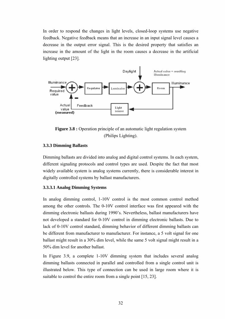
In order to respond the changes in light levels, closed-loop systems use negative feedback. Negative feedback means that an increase in an input signal level causes a decrease in the output error signal. This is the desired property that satisfies an increase in the amount of the light in the room causes a decrease in the artificial lighting output [23].
Figure 3.8 : Operation principle of an automatic light regulation system (Philips Lighting).
3.3.3 Dimming Ballasts
Dimming ballasts are divided into analog and digital control systems. In each system, different signaling protocols and control types are used. Despite the fact that most widely available system is analog systems currently, there is considerable interest in digitally controlled systems by ballast manufacturers.
3.3.3.1 Analog Dimming Systems
In analog dimming control, 1-10V control is the most common control method among the other controls. The 0-10V control interface was first appeared with the dimming electronic ballasts during 1990’s. Nevertheless, ballast manufacturers have not developed a standard for 0-10V control in dimming electronic ballasts. Due to lack of 0-10V control standard, dimming behavior of different dimming ballasts can be different from manufacturer to manufacturer. For instance, a 5 volt signal for one ballast might result in a 30% dim level, while the same 5 volt signal might result in a 50% dim level for another ballast.
In Figure 3.9, a complete 1-10V dimming system that includes several analog dimming ballasts connected in parallel and controlled from a single control unit is illustrated below. This type of connection can be used in large room where it is suitable to control the entire room from a single point [15, 23].

33
Figure 3.9 : Typical 1-10V dimming system [15].
3.3.3.2 Digital Dimming Systems
The digital ballast includes a microcontroller for sending and receiving information digitally according to an interface protocol. Two digital protocols that are directly incorporated into ballasts are the SuperDim protocol by Energy Savings Inc. and the Digitally Addressable Lighting Interface (DALI) by Tridonic Inc. Both protocols use isolated two wire control to carry low voltage control signals. A form of serial communication similar to RS232 method is used in both protocols. Moreover, data rates are 2400 baud for SuperDim and 1200 baud for DALI [15, 16, 23].
The DALI
A system called Digitally Addressable Lighting Interface (DALI) has become a standard that was adopted by several manufacturers. This system allows up to 64 individually addressed ballast connected in parallel to a single two wire bus. Various operating parameters can be changed dynamically in the ballast memory. For instance, scene levels, maximum and minimum brightness can be set for each group of ballast. In large connections, several separate DALI lines can be connected to groups of 64 ballasts controlled by a central controller. Moreover, light sensors and occupancy sensors can be added to control the system automatically [15, 16, 17, 18].

34
Figure 3.10 : Typical DALI dimming system [16].
The DALI includes a bitstream definition for both a forward and backward going messages (Figure 3.11 ). The forward message includes a start bit, 8 address bit, 8 data bits and 2 stop bits. The 8 address bit allows for communication with all off the ballasts at once. The functions performed by the 8 data bits of the forward or backward messages including such features as on-off, dim level and fade time etc.
Figure 3.11 : DALI protocol bit stream definition [16].
Due to increasing interest in the DALI systems, IC manufacturers feel an obligation to develop a solution for digitally addressable digital dimming ballasts using DALI

35
protocol. Microchip and International Rectifier (IR) jointly designed fully functional digitally addressable dimming ballast and prepared a reference design called IRPLDIM2 (Figure 3.12) [15, 16, 18].
Figure 3.12 : IRPLDIM2 Digitally Addressable Dimming Ballast [15, 16].

36
4. AUTOMATIC LUMINOUS FLUX CONTROL SYSTEM
4.1 Introduction
In this section, design and construction of daylight controlled lighting system will be explained and some test results will be given. As mentioned in the previous sections, the daylight based dimming lighting systems has considerable efficiency increase among the other systems. In the system design approach, a composition of the known methods as mentioned in previous sections are considered and tried to apply. The aim of this work is determining the availability of daylight controlled systems in terms of efficiency.
The proposed system is basically “A room with luminaries controlled by an automatic brightness control system” that includes an occupancy or photo sensor, a control center and a luminaries with electronic ballasts as illustrated in Figure 4.1.
Figure 4.1 : The proposed system overview.

37
Figure 4.2 : The block diagram of the proposed system.

38
Figure 4.3 : The overall circuit diagram of proposed system.

39
The main purpose of the system is to control the ambient light level by dimming operation according to the daylight level. As shown in the block diagram of the proposed system in Figure 4.2, the control starts with occupancy and luminance level sense actions. In the sense part, the sense levels are converted into a digital data and transmitted to the control center. The control center determines required frequency for ballasts from the collected sensor data and sends frequency information to the power part. Finally, the driver in the power part gets the frequency data and drives the half bridge circuit to power the lamp. In all parts of the circuit, Microchip PIC16F877 microcontroller is used as a controller. The overall circuit diagram of the proposed system is shown in Figure 4.3.
In fact, the existing lighting and the demonstration site has considerable role in these controls. However, a half or a year long study about the energy behavior of previous existing system is needed for testing the efficiency of future applied system. Moreover, the efficiency studies for daylight controlled systems also needs time and cannot result in a short period time. Therefore, long term efficiency studies are outside the scope of this work. On the other hand, this work is firstly focused on design and construction of a daylight based dimming system. In addition, experimental results of power circuit are given.
4.1.1 Sensor Section
The sensor part is divided into two sections such as occupancy and light sense. To sense the occupancy status, decision is made by a PIR occupancy detector. The occupancy status sensed by detector is a two level logical signal as zero or one.
The luminance level sense is made by light dependent resistor (LDR) and a microcontroller that enables an analog to digital conversion (ADC) into 10 bit resolution. A voltage divider including a LDR and a 10kΩ resistor gives an analog voltage according to sensed light value. The microcontroller ADC part convert the voltage value into 10 bit digital data and sends the most significant 4 bit to the transmit part. Moreover, light sensor part includes a LCD that monitors the current luminance level in term of lux (lumen/m2). The Figure 4.4 illustrates the circuit diagram of light sensor with LCD.

40
Figure 4.4 : Circuit diagram of light sensor.
In the design of voltage divider section, three LDR samples are measured by a lux-meter and an ohm-meter to get the light dependence behavior in different light levels as shown in Table 4.1. The red values are measured and the other values are calculated by using interpolation method.
Table 4.1 : Characteristics of LDR samples.
Sample 1 with a small surface was selected according to its suitable light dependence characteristic. In addition, the ADC pin input voltage change related to LDR impedance value can be calculated for 10kΩ resistance.

41
4.1.2 Control Section
The main purpose of the control part is to determine and transmit the required frequency value to the ballast drivers according to the received light level information from sensors. While the sensor and the power parts can communicate in one way such as sensor to control center or control center to ballast, the control center is able to communicate in both ways. The circuit diagram of control part is illustrated in Figure 4.5.
Figure 4.5 : Circuit diagram of control part
The integrated circuits MC145027 and MC145026 enable the serial communication by decoding and encoding data parallel to serial. The ICs support 5 address bit and 4 data bit for decode and encode operation. Moreover, small hybrid RF circuits are used to communicate with wireless network. The RF transmitter and receiver circuits have a frequency of 434 MHz that is suitable for ballast application.
4.1.3 Power Section
The power section includes two parts such as driver part and ballast circuit part. The driver part operation starts with receiving the operating frequency data in 4 bit resolution. Then, the microcontroller generates the gate drive signals according to the received frequency value to get the desired luminance level. The use of TLP250 gate driver optocouplers can satisfy the requirements of half bridge mosfet switches such as gate signal isolating and strengthening. In order to prevent the short circuit between upper and lower switches during switching, a dead time is required between the two upper and lower switch gate signals. Moreover, an isolated power supply is

42
used for the upper mosfet optocoupler to isolate the upper gate drive circuits from ground. The driver part of power section can be seen in Figure 4.6.
Figure 4.6 : Circuit diagram of driver part
The most important section of the power section is the ballast circuit part that contains a DC link voltage, a half bridge configured mosfet switches and resonant LC circuit with a lamp. The circuit element values are design and selected for a T8-32W fluorescent lamp as mentioned in the previous section.
The frequency value is started with 30 kHz to ignite the lamp and also the operating frequency is changed in a range of 30 kHz to 120 kHz according to the dimming value. The circuit diagram of ballast circuit is illustrated in Figure 4.7. The behavior of the ballast circuit is determined according to the frequency response of LC resonant circuit as mentioned in previous section 2.
Figure 4.7 : Circuit diagram of ballast circuit

43
4.2 Experimental Results of Ballast Test Circuits
In order to understand the behavior of a ballast circuit measurements are made in different operating points and the results are given below. In addition to this, a conventional magnetic ballast circuit is also tested for monitoring the voltage and current values at 50Hz frequency.
In all test circuits, a hall-effect current transducer and a voltage divider are used to monitor current and voltage waveform. However, in the luminous flux change test circuit, the LEM’s voltage transducer LV100-250 which gives 1 volt for an input voltage of 51.8 volts is used to monitor voltage. The LEM’s current transducer HAW03-P gives 1.33 Volts/Amps for current measurement and the resistive voltage divider gives 1 volt for an input voltage of 44.28 volts.
4.2.1 Magnetic Ballast Test Circuit
As shown in Figure 4.8, a magnetic ballast circuit is constructed and tested. The voltage, current and power measurement results for both input and lamp are given below in Table 4.2. In addition, the voltage and current waveforms of the test circuit are shown in Figure 4.9 and Figure 4.10.
Table 4.2 : The measurement results of magnetic ballast test circuit
Figure 4.8 : Setup diagram of the magnetic ballast test circuit

44
Figure 4.9 : Input voltage and current waveforms diagram of the magnetic ballast test circuit
Figure 4.10 : Lamp voltage and current waveforms of the magnetic ballast test circuit

45
4.2.2 Demonstration Ballast Test Circuit
Utility and Lamp Variables versus Frequency Change
In this section, a ballast circuit with 2.5nF capacitor and 1.37mH inductor in the output stage is tested. In test circuit shown in Figure 4.11, demonstration ballast is tested to monitor utility input and lamp input current-voltage waveforms for different operating frequencies.
Figure 4.11 : Setup diagram of the ballast test circuit for utility and lamp variables.
In the test circuit, a driver circuit that enables to change the operating frequency is illustrated in Figure 4.12. The driver circuit generates two square wave signals which are shifted 180 degrees from each other and also the shifted signals should not cross-over. UC3525 satisfies these requirements and also gives a chance to vary the frequency of the signal to dim the lamp during running. Moreover, the frequency response of the ballast output stage during running and ignition is given in Figure 4.13.
Due to the topology of the mosfet’s, an electrical isolation between the upward switch and the driver circuit to prevent a short circuit on the source. Therefore, TLP250 optocouplers are used to isolate the switch signal. In order to isolate the switch signals, the power supply references have to be different for each TLP250. This requirement is satisfied by making different sources for each optocoupler. For each source, a 15 volt transformer, a bridge rectifier, 1000uF capacitor and a 7815 voltage regulator is used.

46
Figure 4.12 : Circuit diagram of the tested ballast circuit.
Figure 4.13 : Frequency response of ballast output stage for L=1.37mH, C=2.5nF.

47
The driver circuit’s two square wave gate signals which are shifted 180 degrees from each other are monitored at different frequencies are shown in below figures.
Figure 4.14 : Gate signal waveforms of the upper and lower mosfets at 120kHz.
Figure 4.15 : Gate signal waveforms of the upper and lower mosfets at 70kHz.

48
Figure 4.16 : Gate signal waveforms of the upper and lower mosfets at 50kHz.
Figure 4.17 : Gate signal waveforms of the upper and lower mosfets at 30kHz.

49
The voltage, current and power measurement results in different frequencies are shown in Table 4.3.
Table 4.3 : The measurement results of ballast circuit for utulity and lamp variables.
Moreover, the V-I waveforms for each frequencies for both utility input and lamp input are given below figures.
Figure 4.18 : Input voltage and current of the ballast at 30kHz.

50
Figure 4.19 : Input voltage and current of the ballast at 50kHz.
Figure 4.20 : Input voltage and current of the ballast at 70kHz.

51
Figure 4.21 : Input voltage and current of the ballast at 100kHz.
Figure 4.22 : Input voltage and current of the ballast at 121kHz.

52
Figure 4.23 : Input voltage and current of the ballast at 132kHz.
Figure 4.24 : Voltage and current of the lamp at 30kHz.

53
Figure 4.25 : Voltage and current of the lamp at 70kHz.
Figure 4.26 : Voltage and current of the lamp at 100kHz.

54
Figure 4.27 : Voltage and current of the lamp at 120kHz.
Figure 4.28 : Voltage and current of the lamp at 132kHz.

55
Luminous Flux versus Frequency Change
In this section, a ballast circuit with 10nF capacitor and 1.37mH inductor in the output stage is tested in an illumination laboratory. In the test circuit shown in Figure 4.29, demonstration ballast is set up to monitor luminous flux change with utility input current-voltage waveforms for different operating frequencies. The lamp is placed in a measurement cube and the luminous flux change is sensed and monitored via a galvanometer deviation. Since, a T8-32W fluorescent lamp draws nearly 33 watts with ballast circuit at maximum luminous flux about 1700 lumens, the frequency value is adjusted to get maximum lamp power. Therefore, the frequency value of 43kHz, is assumed to give the 100% deviation and also the measurement results are recorded with changing frequency. The behavior of the ballast output stage can be understood from the frequency response given in Figure 4.30.
Figure 4.29 : Setup diagram of the ballast test circuit for luminous flux.
Figure 4.30 : Frequency response of ballast output stage for L=1.37mH, C=10nF.

56
The voltage, current and power measurement results in different frequencies are shown in Table 4.4.
Table 4.4 : The measurement results of ballast test circuit for luminous flux change.
Moreover, the V-I waveforms for each frequencies for utility input voltages and currents are given below figures.
Figure 4.31 : Input voltage and current of the ballast at 49.93kHz.

57
Figure 4.32 : Input voltage and current of the ballast at 55.21kHz.
Figure 4.33 : Input voltage and current of the ballast at 58.12kHz.

58
Figure 4.34 : Input voltage and current of the ballast at 59.76kHz.
Figure 4.35 : Input voltage and current of the ballast at 61kHz.

59
Figure 4.36 : Input voltage and current of the ballast at 62.12kHz.
Figure 4.37 : Input voltage and current of the ballast at 62.88kHz.

60
Figure 4.38 : Input voltage and current of the ballast at 63.44kHz.
61
5. CONCLUSION AND FUTURE WORKS
A complete solution of using energy more efficiently in lighting is offered with the study made. A detailed information about the proposed daylight based lighting system was given and also some test result was given. The proposed system can satisfy the expected needs of a daylight controlled lighting system such as self-dimming and manual dimming. Since, the control operations are made by microcontrollers, the system becomes more flexible and easy to update. Moreover, the wireless RF configuration enables an easy made system installation without a cable requirement. The communication ICs make the system connections more flexible that a number of 32 different sensors or electronic ballasts can be controlled from the control center.
In fact, the aim of this work is learning the availibity of daylight controlled systems in terms of efficiency. However, the efficiency studies for automatic controlled systems needs a minimum half or a year energy consumption information. Moreover, a long term energy consumption knowledge of previous existing system is needed to compare with the efficiency of future applied system. Therefore, efficiency studies cannot be mentioned in this work.
In conclusion, a daylight configured automatic dimming control system is designed and constructs to show efficiency of these systems. Moreover, the proposed system power part was tested and the results were given.
The future works that can improve the study made will be :
- A long term energy consumption study to learn system efficiency
- An EMI filter and a power factor correction circuit
- A RS232 connection with a computer

62
REFERENCES
[1] Kularatna, N., 1998. Power Electronics Design Handbook: Low Power Components and Applications, Buterworth-Heineman.
[2] Meyer, C., Nienhuis, H., 1998. Discharge Lamps, Philips Technical Library.
[3] F. Rubinstein, M. Siminovitch, R. Verderber. 1993. Fifty Percent Energy Savings with Automatic Lighting Controls. IEEE Trans. Industry Applications, vol. 29, no. 4, pp.768-773, 1993.
[4] L.D. Jennings, F. Rubinstein, D. DiBartolomeo, S. Blanc. 1999. Comparison of Control Options in Private Offices in an Advanced Lighting Controls Tested, IESNA Annual Conference, August 1999.
[5] E. S. Lee, S. E. Selkowitz. 2005 The New York Times Headquarters Daylighting Mockup: Monitored performance of the daylighting control system. Building Technologies Program, February 2005.
[6] Daylighting the New York Times Headquarters Building-LBNL project website: http://windows.lbl.gov/comm_perf/newyorktimes.htm
[7] Erickson R. W., 2000. Fundamentals of Power Electronics. Kluwer Academic Publishers-Massachusetts
[8] Zhou J., 2003. Electronic Ballast for Fluorescent Lamps: An Undergraduate Instructional Module, Center of Power Electronics, Virginia Tech.
[9] Ribarich T. J. and Ribarich J. J., 1997. A new Procedure for High-Frequency Electronic Ballast , IEEE Industry Applications Society Annual Meeting.
[10] Tam P. W., Lee T. S., Hui S. Y. R., Chung H. S. H. and Liu Y. S., 2003. Practical Evaluation of Dimming Control Methods for Electronic Ballast , IEEE.

63
[11] Ribarich T., 2006. How to Design a Dimming Fluorescent Electronic Ballast, International Rectifier Technical Paper.
[12] Cook B., 1998. High-efficiency Lighting in Industry and Commercial Buildings, Power Engineering Journal.
[13] Ribarich T., 1999. A Systems Approach to Ballast IC Design As presented at PCIM Europe.
[14] Tröstl A., 2001. Self Configuring Dimming Interface For Fluorescent Lamp Ballast. IEEE.
[15] Ribarich T. J., 2002. Analog and Digital Fluorescent Lighting Dimming Systems. International Rectifier Technical Paper.
[16] Green P., 2005. Digital Control Turns On the Lights, Power Electronics Technology.
[17] Contenti C. and Ribarich T., 2002. Digitally Addressable DALI Dimming Ballast. Presented at APEC 2002.
[18] Contenti C., Ribarich T. and Fosler R., 2003. Digital Dimming DALI Ballast For 36W/T8 220V input. International Rectifier Reference Design.
[19] Liang T. J., Liu T. S. and Chang F., 1997. Design and Analysis of Dimming Electronic Ballast. IEEE Industry Applications Magazine.
[20] Moo C. S., Member, IEEE, Lin T. S., Cheng H. L. and Soong M. J., 2001. Electronic Ballast for Programmed Rapid-Start Fluorescent Lamps. IEEE Industry Applications Magazine.
[21] Costa M. A. D., Landerdahl M. L. Jr. and Prado R. N. 2002. Independent Multi-Lamp Electronic Ballast. IEEE Industry Applications Magazine.
[22] Brioschi R. O. and Vieira J. L. F., 1998. High-Power-Factor Electronic Ballast with Constat DC-Link Voltage. IEEE Industry Applications Magazine.

64
[23] Reducing Barriers to Use of High Efficiency Lighting Systems, 2001, Lighting Research Center - Rensselaer Polytechnic Institute website: http://www.lrc.rpi.edu/researchtopics/reducingBarriers/barriersToImplementation.asp
[24] Advanced Lighting Guidelines, 2003 - New Buildings Institute website: http://www.newbuildings.com/downloads/ALG_2003.htm.

65
APPENDIX A
Measurement Tranducer Datasheets

Voltage Transducer LV 100-250For the electronic measurement of voltages : DC, AC, pulsed...,with a galvanic isolation between the primary circuit (high voltage)and the secondary circuit (electronic circuit).
Electrical data
VPN
Primary nominal r.m.s. voltage 250 VV
PPrimary voltage, measuring range 0 .. ± 375 V
IPN
Primary nominal r.m.s. current 40 mAR
MMeasuring resistance R
M minR
M max
with ± 15 V @ ± 250 V max
0 170 Ω@ ± 375 V
max0 90 Ω
ISN
Secondary nominal r.m.s. current 50 mAK
NConversion ratio 250 V / 50 mA
VC
Supply voltage (± 5 %) ± 15 VIC
Current consumption 10 + IS
mAV
dR.m.s. voltage for AC isolation test, 50 Hz, 1 mn 6 kV
Accuracy - Dynamic performance data
X G
Overall Accuracy @ VPN
, TA = 25°C ± 0.7 %
εL
Linearity < 0.1 %
Typ MaxIO
Offset current @ IP = 0, T
A = 25°C ± 0.3 mA
IOT
Thermal drift of IO
0°C .. + 70°C ± 0.2 ± 0.3 mA
tr
Response time @ 90 % of V
P max75 µs
General data
TA
Ambient operating temperature 0 .. + 70 °CT
SAmbient storage temperature - 25 .. + 85 °C
N Turns ratio 2500 : 2000P Total primary power loss 10 WR
1Primary resistance @ T
A = 25°C 6.25 kΩ
R S
Secondary coil resistance @ TA
= 70°C 60 Ωm Mass 850 g
Standards 1) EN 50178
Note : 1) A list of corresponding tests is available
Features
•Closed loop (compensated) voltagetransducer using the Hall effect
•Insulated plastic case recognizedaccording to UL 94-V0
•Primary resistor R 1 incorporated intothe housing.
Advantages
•Excellent accuracy•Very good linearity•Low thermal drift•High immunity to external
interference.
Applications
•AC variable speed drives and servomotor drives
•Static converters for DC motor drives•Uninterruptible Power Supplies
(UPS)•Power supplies for welding
applications.
980709/1
VPN = 250 V
LEM Components www.lem.com

Front view
Top view
Left view
Dimensions LV 100-250 (in mm. 1 mm = 0.0394 inch)
Remarks
•IS is positive when V
P is applied on terminal +HT.
•The primary circuit of the transducer must be linked to theconnections where the voltage has to be measured.
•This is a standard model. For different versions (supplyvoltages, turns ratios, unidirectional measurements...),please contact us.
Secondary terminals
Terminal + : supply voltage + 15 VTerminal M : measureTerminal - : supply voltage - 15 VTerminal : ground or earth
Connection
LEM reserves the right to carry out modifications on its transducers, in order to improve them, without previous notice.
Mechanical characteristics
•General tolerance ± 0.3 mm•Fastening 2 holes ∅ 6.5 mm•Connection of primary M5 threaded studs•Connection of secondary Faston 6.3 x 0.8 mm•Connection to the ground M5 threaded stud•Fastening torque 2.2 Nm or 1.62 Lb. -Ft.

Electrical data
Primary nominal Primary current Primary Conductor Typer.m.s. current measuring range Diameter I
PN (A) I
P (A) (mm)
3 ± 7.5 0.8 HAW 03-P5 ± 13 0.9 HAW 05-P
10 ± 25 1.1 HAW 10-P15 ± 38 1.4 HAW 15-P20 ± 50 1.6 HAW 20-P
VC
Supply voltage (± 5 %) ± 15 VI C
Current consumption <± 18 mAV
dR.m.s. voltage for AC isolation test, 50/60Hz, 1 mn 2.0 kV
R IS
Isolation resistance @ 500 VDC > 500 MΩV
OUTOutput voltage @ ± I
PN, R
L = 10 kΩ, T
A = 25°C ±4 V
ROUT
Output internal resistance 100 ΩR
LLoad resistance >10 kΩ
Accuracy-Dynamic performance data
X Accuracy @ IPN
, TA = 25°C (without offset) < ± 1 % of I
PNεεL
Linearity (0 .. ± IPN
) < ± 1 % of IPN
VOE
Electrical offset voltage, TA = 25°C < ± 40 mV
VOH
Hysteresis offset voltage @ IP
= 0;after an excursion of 1 x I
PN< ± 20 mV
VOT
Thermal drift of VOE
max. ± 1.5 mV/K
TCεεG
Thermal drift of the gain (% of reading) ± 0.1 %/K
t r
Response time @ 90% of IP
< 3 µsf Frequency bandwidth (- 3 dB)1) DC .. 50 kHz
General data
TA
Ambient operating temperature - 10 .. + 75 °CT
SAmbient storage temperature - 15 .. + 85 °C
m Mass 12 g
Current Transducer HAW 03 .. 20-PFor the electronic measurement of currents: DC, AC, pulsed, mixed,with a galvanic isolation between the primary circuit (high power) andthe secondary circuit (electronic circuit).
IPN = 3 .. 20 A
Features
• Hall effect measuring principle• Galvanic isolation between primary
and secondary circuit• Isolation voltage 2000 V• Low power consumption• Extended measuring range(2.5x I
PN)
Advantages
• Easy mounting• Small size and space saving• Only one design for wide current
ratings range• High immunity to external
interference.
Applications
• DC motor drives• Switched Mode Power Supplies
(SMPS)• AC variable speed drives• Uninterruptible Power Supplies (UPS)• Battery supplied applications• Inverters
Notes : EN 50178 approval pending
LEM Components www.lem.com
010118/2
1) Derating is needed to avoid excessive core heating at high frequency.

HAW 03 .. 20-P
LEM reserves the right to carry out modifications on its transducers, in order to improve them, without previousnotice.
0.5
1234
6 +
/-1
4.5
+/-
1
Primary Conductor
4-0.5*0.25
Terminal Pin Identification
UNIT : mm
SCALE : 2/1
19 +/-1
2
0 +
/-1
2
15 +/-1
Signal Pins
Primary ConductorPart No. DiameterHAW 03-PHAW 05-PHAW 10-PHAW 15-PHAW 20-P
0.8 d0.9 d1.1 d1.4 d1.6 d
See the attached table
2.5
+/-
1
56 78
Pin No.5-65-67-87-87-8
Signal Pins
3 +Vcc
1 -Vcc
4 Output
2 0V
5 (+) 6 (-)
7 (+) 8 (-)
Direction of Current Flow
15 +/-1
6 +/-1
1
1 +
/-1
3-p=2.54
Front View Right View
Bottom View

70
APPENDIX B
Datasheets of ICs Used in Circuit

TL/H/7746
LM
78X
XSerie
sV
olta
ge
Regula
tors
February 1995
LM78XX Series Voltage Regulators
General DescriptionThe LM78XX series of three terminal regulators is available
with several fixed output voltages making them useful in a
wide range of applications. One of these is local on card
regulation, eliminating the distribution problems associated
with single point regulation. The voltages available allow
these regulators to be used in logic systems, instrumenta-
tion, HiFi, and other solid state electronic equipment. Al-
though designed primarily as fixed voltage regulators these
devices can be used with external components to obtain
adjustable voltages and currents.
The LM78XX series is available in an aluminum TO-3 pack-
age which will allow over 1.0A load current if adequate heat
sinking is provided. Current limiting is included to limit the
peak output current to a safe value. Safe area protection for
the output transistor is provided to limit internal power dissi-
pation. If internal power dissipation becomes too high for
the heat sinking provided, the thermal shutdown circuit
takes over preventing the IC from overheating.
Considerable effort was expanded to make the LM78XX se-
ries of regulators easy to use and mininize the number
of external components. It is not necessary to bypass the
output, although this does improve transient response. Input
bypassing is needed only if the regulator is located far from
the filter capacitor of the power supply.
For output voltage other than 5V, 12V and 15V the LM117
series provides an output voltage range from 1.2V to 57V.
FeaturesY Output current in excess of 1AY Internal thermal overload protectionY No external components requiredY Output transistor safe area protectionY Internal short circuit current limitY Available in the aluminum TO-3 package
Voltage RangeLM7805C 5V
LM7812C 12V
LM7815C 15V
Schematic and Connection Diagrams
TL/H/7746–1
Metal Can Package
TO-3 (K)
Aluminum
TL/H/7746–2
Bottom View
Order Number LM7805CK,
LM7812CK or LM7815CK
See NS Package Number KC02A
Plastic Package
TO-220 (T)
TL/H/7746–3
Top View
Order Number LM7805CT,
LM7812CT or LM7815CT
See NS Package Number T03B
C1995 National Semiconductor Corporation RRD-B30M115/Printed in U. S. A.

Absolute Maximum RatingsIf Military/Aerospace specified devices are required,
please contact the National Semiconductor Sales
Office/Distributors for availability and specifications.
Input Voltage (VO e 5V, 12V and 15V) 35V
Internal Power Dissipation (Note 1) Internally Limited
Operating Temperature Range (TA) 0§C to a70§C
Maximum Junction Temperature
(K Package) 150§C(T Package) 150§C
Storage Temperature Range b65§C to a150§CLead Temperature (Soldering, 10 sec.)
TO-3 Package K 300§CTO-220 Package T 230§C
Electrical Characteristics LM78XXC (Note 2) 0§C s Tj s 125§C unless otherwise noted.
Output Voltage 5V 12V 15V
Input Voltage (unless otherwise noted) 10V 19V 23V Units
Symbol Parameter Conditions Min Typ Max Min Typ Max Min Typ Max
VO Output Voltage Tj e 25§C, 5 mA s IO s 1A 4.8 5 5.2 11.5 12 12.5 14.4 15 15.6 V
PD s 15W, 5 mA s IO s 1A 4.75 5.25 11.4 12.6 14.25 15.75 V
VMIN s VIN s VMAX (7.5 s VIN s 20) (14.5 s VIN s 27) (17.5 s VIN s 30) V
DVO Line Regulation IO e 500 mA Tj e 25§C 3 50 4 120 4 150 mV
DVIN (7 s VIN s 25) 14.5 s VIN s 30) (17.5 s VIN s 30) V
0§C s Tj s a125§C 50 120 150 mV
DVIN (8 s VIN s 20) (15 s VIN s 27) (18.5 s VIN s 30) V
IO s 1A Tj e 25§C 50 120 150 mV
DVIN (7.5 s VIN s 20) (14.6 s VIN s 27) (17.7 s VIN s 30) V
0§C s Tj s a125§C 25 60 75 mV
DVIN (8 s VIN s 12) (16 s VIN s 22) (20 s VIN s 26) V
DVO Load Regulation Tj e 25§C 5 mA s IO s 1.5A 10 50 12 120 12 150 mV
250 mA s IO s 750 mA 25 60 75 mV
5 mA s IO s 1A, 0§C s Tj s a125§C 50 120 150 mV
IQ Quiescent Current IO s 1A Tj e 25§C 8 8 8 mA
0§C s Tj s a125§C 8.5 8.5 8.5 mA
DIQ Quiescent Current 5 mA s IO s 1A 0.5 0.5 0.5 mA
ChangeTj e 25§C, IO s 1A 1.0 1.0 1.0 mA
VMIN s VIN s VMAX (7.5 s VIN s 20) (14.8 s VINs 27) (17.9 s VIN s 30) V
IO s 500 mA, 0§C s Tj s a125§C 1.0 1.0 1.0 mA
VMIN s VIN s VMAX (7 s VIN s 25) (14.5 s VINs 30) (17.5 s VIN s 30) V
VN Output Noise Voltage TA e25§C, 10 Hz s f s 100 kHz 40 75 90 mV
DVIN
DVOUT
Ripple Rejection IO s 1A, Tj e 25§C or 62 80 55 72 54 70 dB
f e 120 Hz IO s 500 mA 62 55 54 dBÐ 0§C s Tj s a125§CVMIN s VIN s VMAX (8 s VIN s 18) (15 s VIN s 25) (18.5 s VIN s 28.5) V
RO Dropout Voltage Tj e 25§C, IOUT e 1A 2.0 2.0 2.0 V
Output Resistance f e 1 kHz 8 18 19 mX
Short-Circuit Current Tj e 25§C 2.1 1.5 1.2 A
Peak Output Current Tj e 25§C 2.4 2.4 2.4 A
Average TC of VOUT 0§C s Tj s a125§C, IO e 5 mA 0.6 1.5 1.8 mV/§C
VIN Input Voltage
Required to Maintain Tj e 25§C, IO s 1A 7.5 14.6 17.7 V
Line Regulation
Note 1: Thermal resistance of the TO-3 package (K, KC) is typically 4§C/W junction to case and 35§C/W case to ambient. Thermal resistance of the TO-220
package (T) is typically 4§C/W junction to case and 50§C/W case to ambient.
Note 2: All characteristics are measured with capacitor across the input of 0.22 mF, and a capacitor across the output of 0.1mF. All characteristics except noise
voltage and ripple rejection ratio are measured using pulse techniques (tw s 10 ms, duty cycle s 5%). Output voltage changes due to changes in internal
temperature must be taken into account separately.
2

TL/H/7340
LM
79X
XSerie
s3-T
erm
inalN
egativ
eR
egula
tors
November 1994
LM79XX Series 3-Terminal Negative Regulators
General DescriptionThe LM79XX series of 3-terminal regulators is available with
fixed output voltages of b5V, b8V, b12V, and b15V.
These devices need only one external componentÐa com-
pensation capacitor at the output. The LM79XX series is
packaged in the TO-220 power package and is capable of
supplying 1.5A of output current.
These regulators employ internal current limiting safe area
protection and thermal shutdown for protection against vir-
tually all overload conditions.
Low ground pin current of the LM79XX series allows output
voltage to be easily boosted above the preset value with a
resistor divider. The low quiescent current drain of
these devices with a specified maximum change with line
and load ensures good regulation in the voltage boosted
mode.
For applications requiring other voltages, see LM137 data
sheet.
FeaturesY Thermal, short circuit and safe area protectionY High ripple rejectionY 1.5A output currentY 4% tolerance on preset output voltage
Connection Diagrams
TO-220 Package
TL/H/7340–14
Front View
Order Number LM7905CT, LM7912CT or LM7915CT
See NS Package Number TO3B
Typical Applications
Fixed Regulator
TL/H/7340–3
*Required if regulator is separated from filter capacitor by
more than 3×. For value given, capacitor must be solid
tantalum. 25 mF aluminum electrolytic may be substituted.
²Required for stability. For value given, capacitor must be
solid tantalum. 25 mF aluminum electrolytic may be substi-
tuted. Values given may be increased without limit.
For output capacitance in excess of 100 mF, a high current
diode from input to output (1N4001, etc.) will protect the
regulator from momentary input shorts.
C1995 National Semiconductor Corporation RRD-B30M115/Printed in U. S. A.

Absolute Maximum Ratings (Note 1)
If Military/Aerospace specified devices are required,
please contact the National Semiconductor Sales
Office/Distributors for availability and specifications.
Input Voltage
(Vo e b5V) b25V
(Vo e b12V and b15V) b35V
Input-Output Differential
(Vo e b5V) 25V
(Vo e b12V and b15V) 30V
Power Dissipation (Note 2) Internally Limited
Operating Junction Temperature Range 0§C to a125§CStorage Temperature Range b65§C to a150§CLead Temperature (Soldering, 10 sec.) 230§C
Electrical Characteristics Conditions unless otherwise noted: IOUT e 500 mA, CIN e 2.2 mF, COUT e 1 mF,
0§C s TJ s a125§C, Power Dissipation s 1.5W.
Part Number LM7905C
UnitsOutput Voltage b5V
Input Voltage (unless otherwise specified) b10V
Symbol Parameter Conditions Min Typ Max
VO Output Voltage TJ e 25§C b4.8 b5.0 b5.2 V
5 mA s IOUT s 1A, b4.75 b5.25 V
P s 15W (b20 s VIN s b7) V
DVO Line Regulation TJ e 25§C, (Note 3) 8 50 mV
(b25 s VIN s b7) V
2 15 mV
(b12 s VIN s b8) V
DVO Load Regulation TJ e 25§C, (Note 3)
5 mA s IOUT s 1.5A 15 100 mV
250 mA s IOUT s 750 mA 5 50 mV
IQ Quiescent Current TJ e 25§C 1 2 mA
DIQ Quiescent Current With Line 0.5 mA
Change (b25 s VIN s b7) V
With Load, 5 mA s IOUT s 1A 0.5 mA
Vn Output Noise Voltage TA e 25§C, 10 Hz s f s 100 Hz 125 mV
Ripple Rejection f e 120 Hz 54 66 dB
(b18 s VIN s b8) V
Dropout Voltage TJ e 25§C, IOUT e 1A 1.1 V
IOMAX Peak Output Current TJ e 25§C 2.2 A
Average Temperature IOUT e 5 mA, 0.4 mV/§CCoefficient of 0 C s TJ s 100§COutput Voltage
Typical Applications (Continued)
Variable Output
TL/H/7340–2*Improves transient response and ripple rejection. Do not increase beyond 50 mF.
VOUT e VSET #R1 a R2
R2 JSelect R2 as follows:
LM7905CT 300X
LM7912CT 750X
LM7915CT 1k
2

©2000 Fairchild Semiconductor International
www.fairchildsemi.com
Rev. 5.0
Features• 5V ± 1% Reference• Oscillator Sync terminal• Internal Soft Start• Deadtime Control• Under-Voltage Lockout
DescriptionUC3525A is a monolithic integrated circuit that Included all of the control circuit necessary for a pulse width modulat-ing regulator. There are a voltage reference, an error ampli-fier, a pulse width modulator, an oscillator, under-voltage lockout, soft start circuit, and output drivers in the chip.
16-DIP
1
Internal Block Diagram
UC3525ASMPS Controller

UC3525A
2
Absolute Maximum Ratings
Electrical Characteristics(VCC = 20V, TA = -30°C to + 85°C, unless otherwise specified)
Parameter Symbol Value Unit
Supply Voltage VCC 40 V
Collector Supply Voltage VC 40 V
Output Current, Sink or Source IO 500 mA
Reference Output Current IREF 50 mA
Oscillator Charging Current ICHG(OSC) 5 mA
Power Dissipation (TA = 25°C) PD 1000 m/W
Operating Temperature TOPR 0 ~ +70 °CStorage Temperature TSTG -65 ~ +150 °CLead Temperature (Soldering, 10 sec) TLEAD +300 °C
Parameter Symbol Conditions Min. Typ. Max. Unit
REFERENCE SECTION
Reference Output Voltage VREF TJ = 25°C 5.0 5.1 5.2 V
Line Regulation ∆VREF VCC = 8 to 35V - 9 20 mV
Load Regulation ∆VREF IREF = 0 to 20mA - 20 50 mV
Short Circuit Output Current ISC VREF = 0, TJ = 25°C - 80 100 mA
Total Output Variation (Note 1) ∆VREF Line, Load and Temperature 4.95 - 5.25 V
Temperature Stability (Note 1) STT - - 20 50 mV
Long Term Stability (Note 1) ST TJ = 125°C ,1 KHRS - 20 50 mV
OSCILLATOR SECTION
Initial Accuracy (Note 1, 2) ACCUR TJ = 25°C - ± 3 ± 6 %
Frequency Change With Voltage ∆f/∆VCC VCC = 8 to 35V (Note 1, 2) - ± 0.8 ± 2 %
Maximum Frequency f(MAX) RT = 2KΩ, CT = 470pF 400 430 - KHz
Minimum Frequency f(MIN) RT = 200KΩ, CT = 0.1uF - 60 120 Hz
Clock Amplitude (Note 1, 2) V(CLK) - 3 4 - V
Clock Width (Note 1, 2) tW(CLK) TJ = 25°C 0.3 0.6 1 µs
Sync Threshold VTH(SYNC) - 1.2 2 2.8 V
Sync Input Current II(SYNC) Sync = 3.5V - 1.3 2.5 mA

UC3525A
3
Electrical Characteristics(VCC = 20V, TA = 0 to +85°C, unless otherwise specified)
Notes :1. These parameters. although guaranteed over the recommended operating conditions, are not 100% tested in production2. Tested at fOSC=40 KHz (RT =3.6K, CT =0.01uF, RI = 0Ω)
Parameter Symbol Conditions Min. Typ. Max. Unit
ERROR AMPLIFIER SECTION (VCM = 5.1V)
Input Offset Voltage VIO - - 1.5 10 mV
Input Bias Current IBIAS - - 1 10 µA
Input Offset Current IIO - - 0.1 1 µA
Open Loop Voltage Gain GVO RL ≥10MΩ 60 80 - dB
Common Mode Rejection Ratio CMRR VCM = 1.5 to 5.2V 60 90 - dB
Power Supply Rejection Ratio PSRR VCC = 8 to 3.5V 50 60 - dB
PWM COMPARATOR SECTION
Minimum Duty Cycle D(MIN) - - - 0 %
Maximum Duty Cycle D(MAX) - 45 49 - %
Input Threshold Voltage (Note 2) VTH1 Zero Duty Cycle 0.7 0.9 - V
Input Threshold Voltage (Note 2) VTH2 Max Duty Cycle - 3.2 3.6 V
SOFT-START SECTION
Soft Start Current ISOFT VSD = 0V, VSS = 0V 25 51 80 µA
Soft Start Low Level Voltage VSL VSD = 25V - 0.3 0.7 V
Shutdown Threshold Voltage VTH(SD) - 0.6 0.8 1 V
Shutdown Input Current IN(SD) VSD = 2.5V - 0.3 1 mA
OUTPUT SECTION
Low Output Voltage I VOL I ISINK = 20mA - 0.1 0.4 V
Low Output Voltage II VOL II ISINK = 100mA - 0.05 2 V
High Output Voltage I VCH I ISOURCE = 20mA 18 19 - V
High Output Voltage II VCH II ISOURCE = 100mA 17 18 - V
Under Voltage Lockout VUV V8 and V9 = High 6 7 8 V
Collector Leakage Current ILKG VCC = 35V - 80 200 µA
Rise Time (Note 1) tR CL = 1uF, TJ = 25°C - 80 600 ns
Fall Time (Note 1) tF CL = 1uF, TJ = 25°C - 70 300 ns
STANDBY CURRENT
Supply Current ICC VCC = 35V - 12 20 mA

©2002 Fairchild Semiconductor Corporation IRF840 Rev. B
IRF840
8A, 500V, 0.850 Ohm, N-Channel Power MOSFET
This N-Channel enhancement mode silicon gate power field effect transistor is an advanced power MOSFET designed, tested, and guaranteed to withstand a specified level of energy in the breakdown avalanche mode of operation. All of these power MOSFETs are designed for applications such as switching regulators, switching converters, motor drivers, relay drivers, and drivers for high power bipolar switching transistors requiring high speed and low gate drive power. These types can be operated directly from integrated circuits.
Formerly developmental type TA17425.
Features
• 8A, 500V
• r
DS(ON)
= 0.850
Ω
• Single Pulse Avalanche Energy Rated
• SOA is Power Dissipation Limited
• Nanosecond Switching Speeds
• Linear Transfer Characteristics
• High Input Impedance
• Related Literature- TB334 “Guidelines for Soldering Surface Mount
Components to PC Boards”
Symbol
Packaging
JEDEC TO-220AB
TOP VIEW
Ordering Information
PART NUMBER PACKAGE BRAND
IRF840 TO-220AB IRF840
NOTE: When ordering, include the entire part number. G
D
S
SOURCEDRAIN
GATE
DRAIN(FLANGE)
Data Sheet January 2002

IRF840 Rev. B
Absolute Maximum Ratings
T
C
= 25
o
C, Unless Otherwise Specified
IRF840 UNITS
Drain to Source Voltage (Note 1) . . . . . . . . . . . . . . . . . . . . . . . . . . . . . . . . . . . . . . . . . . . . . . . . . . . . . . .V
DS
500 VDrain to Gate Voltage (R
GS
= 20k
Ω)
(Note 1) . . . . . . . . . . . . . . . . . . . . . . . . . . . . . . . . . . . . . . . . . . . V
DGR
500 VContinuous Drain Current . . . . . . . . . . . . . . . . . . . . . . . . . . . . . . . . . . . . . . . . . . . . . . . . . . . . . . . . . . . . . I
D
8.0 AT
C
= 100
o
C . . . . . . . . . . . . . . . . . . . . . . . . . . . . . . . . . . . . . . . . . . . . . . . . . . . . . . . . . . . . . . . . . . . . . . I
D
5.1 APulsed Drain Current (Note 3) . . . . . . . . . . . . . . . . . . . . . . . . . . . . . . . . . . . . . . . . . . . . . . . . . . . . . . . . . I
DM
32 AGate to Source Voltage . . . . . . . . . . . . . . . . . . . . . . . . . . . . . . . . . . . . . . . . . . . . . . . . . . . . . . . . . . . . . .V
GS
±
20 VMaximum Power Dissipation . . . . . . . . . . . . . . . . . . . . . . . . . . . . . . . . . . . . . . . . . . . . . . . . . . . . . . . . . . .P
D
125 WLinear Derating Factor . . . . . . . . . . . . . . . . . . . . . . . . . . . . . . . . . . . . . . . . . . . . . . . . . . . . . . . . . . . . . . . . . . 1.0 W/
o
CSingle Pulse Avalanche Energy Rating (Note 4) . . . . . . . . . . . . . . . . . . . . . . . . . . . . . . . . . . . . . . . . . . .E
AS
510 mJOperating and Storage Temperature . . . . . . . . . . . . . . . . . . . . . . . . . . . . . . . . . . . . . . . . . . . . . . . T
J
, T
STG
-55 to 150
o
CMaximum Temperature for Soldering
Leads at 0.063in (1.6mm) from Case for 10s. . . . . . . . . . . . . . . . . . . . . . . . . . . . . . . . . . . . . . . . . . . . . T
L
Package Body for 10s, See Techbrief 334 . . . . . . . . . . . . . . . . . . . . . . . . . . . . . . . . . . . . . . . . . . . . . T
pkg
300260
o
C
o
C
CAUTION: Stresses above those listed in “Absolute Maximum Ratings” may cause permanent damage to the device. This is a stress only rating and operation of thedevice at these or any other conditions above those indicated in the operational sections of this specification is not implied.
NOTE:
1. T
J
= 25
o
C to 125
o
C.
Electrical Specifications
T
C
= 25
o
C, Unless Otherwise Specified
PARAMETER SYMBOL TEST CONDITIONS MIN TYP MAX UNITS
Drain to Source Breakdown Voltage BV
DSS
V
GS
= 0V, I
D
= 250
µ
A (Figure 10) 500 - - V
Gate to Threshold Voltage V
GS(TH)
V
GS
= V
DS
, I
D
= 250
µ
A 2.0 - 4.0 V
Zero-Gate Voltage Drain Current I
DSS
V
DS
= Rated BV
DSS
, V
GS
= 0V - - 25
µ
A
V
DS
= 0.8 x Rated BV
DSS
, V
GS
= 0V, T
J
= 125
o
C - - 250
µ
A
On-State Drain Current (Note 2) I
D(ON)
V
DS
> I
D(ON) x
r
DS(ON)MAX
, V
GS
= 10V 8.0 - - A
Gate to Source Leakage Current I
GSS
V
GS
=
±
20V - -
±
100 nA
Drain to Source On Resistance (Note 2) r
DS(ON)
V
GS
= 10V, I
D
= 4.4A (Figures 8, 9) - 0.8 0.85
Ω
Forward Transconductance (Note 2) g
fs
V
DS
≥
50V, I
D
= 4.4A (Figure 12) 4.9 7.4 - S
Turn-On Delay Time t
D(ON)
V
DD
=
250V, I
D
≈
8A, R
G
= 9.1
Ω
, R
L
= 30
Ω
MOSFET Switching Times are Essentially Independent of Operating Temperature.
- 15 21 ns
Rise Time t
r
- 21 35 ns
Turn-Off Delay Time t
D(OFF)
- 50 74 ns
Fall Time t
f
- 20 30 ns
Total Gate Charge (Gate to Source + Gate to Drain)
Q
g(TOT)
V
GS
= 10V, I
D
= 8A, V
DS
= 0.8 x Rated BV
DSS
I
g(REF)
= 1.5mA (Figure 14) Gate Charge is Essentially Independent of Operating Temperature
- 42 63 nC
Gate to Source Charge Q
gs
- 7.0 - nC
Gate to Drain “Miller” Charge Q
gd
- 22 - nC
Input Capacitance C
ISS
V
GS
= 0V, V
DS
= 25V, f = 1.0MHz (Figure 11) - 1225 - pF
Output Capacitance C
OSS
- 200 - pF
Reverse-Transfer Capacitance C
RSS
- 85 - pF
Internal Drain Inductance L
D
Measured from the Contact Screw on Tab to Center of Die
Modified MOSFET Symbol Showing the Internal Devices Inductances
- 3.5 - nH
Measured from the Drain Lead, 6mm (0.25in) from Package to Center of Die
- 4.5 - nH
Internal Source Inductance L
S
Measured from the Source Lead, 6mm (0.25in) from Header to Source Bonding Pad
- 7.5 - nH
Thermal Resistance Junction to Case R
θ
JC
- - 1.0
o
C/W
Thermal Resistance Junction to Ambient R
θ
JA
Free Air Operation - - 62.5
o
C/W
LS
LD
G
D
S
IRF840

TLP250
2004-06-25 1
TOSHIBA Photocoupler GaAlAs Ired & Photo−IC
TLP250
Transistor Inverter Inverter For Air Conditionor IGBT Gate Drive Power MOS FET Gate Drive The TOSHIBA TLP250 consists of a GaAlAs light emitting diode and a integrated photodetector. This unit is 8−lead DIP package. TLP250 is suitable for gate driving circuit of IGBT or power MOS FET. • Input threshold current: IF=5mA(max.) • Supply current (ICC): 11mA(max.) • Supply voltage (VCC): 10−35V • Output current (IO): ±1.5A (max.) • Switching time (tpLH/tpHL): 1.5µs(max.) • Isolation voltage: 2500Vrms(min.) • UL recognized: UL1577, file No.E67349 • Option (D4) type VDE approved: DIN VDE0884/06.92,certificate No.76823 Maximum operating insulation voltage: 630VPK Highest permissible over voltage: 4000VPK
(Note) When a VDE0884 approved type is needed, please designate the "option (D4)"
• Creepage distance: 6.4mm(min.) Clearance: 6.4mm(min.)
Schmatic Pin Configuration (top view)
8
7
6
5
1 : N.C. 2 : Anode 3 : Cathode 4 : N.C. 5 : GND 6 : VO (Output) 7 : VO 8 : VCC
1
2
3
4
2+
VF
IF
3-
ICC
(Tr 1)
VO
GND
(Tr 2) IO
VO
VCC8
7
6
5A 0.1µF bypass capcitor must be connected between pin 8 and 5 (See Note 5).
Truth Table
Tr1 Tr2
On On Off Input LED Off Off On
Unit in mm
TOSHIBA 11−10C4
Weight: 0.54 g

TLP250
2004-06-25 2
Absolute Maximum Ratings (Ta = 25°C)
Characteristic Symbol Rating Unit
Forward current IF 20 mA
Forward current derating (Ta ≥ 70°C) ∆IF / ∆Ta −0.36 mA / °C
Peak transient forward curent (Note 1) IFPT 1 A
Reverse voltage VR 5 V
LED
Junction temperature Tj 125 °C
“H”peak output current (PW ≤ 2.5µs,f ≤ 15kHz) (Note 2) IOPH −1.5 A
“L”peak output current (PW ≤ 2.5µs,f ≤ 15kHz) (Note 2) IOPL +1.5 A
(Ta ≤ 70°C) 35 Output voltage
(Ta = 85°C) VO
24 V
(Ta ≤ 70°C) 35 Supply voltage
(Ta = 85°C) VCC
24 V
Output voltage derating (Ta ≥ 70°C) ∆VO / ∆Ta −0.73 V / °C
Supply voltage derating (Ta ≥ 70°C) ∆VCC / ∆Ta −0.73 V / °C
Det
ecto
r
Junction temperature Tj 125 °C
Operating frequency (Note 3) f 25 kHz
Operating temperature range Topr −20~85 °C
Storage temperature range Tstg −55~125 °C
Lead soldering temperature (10 s) (Note 4) Tsol 260 °C
Isolation voltage (AC, 1 min., R.H.≤ 60%) (Note 5) BVS 2500 Vrms
Note 1: Pulse width PW ≤ 1µs, 300pps
Note 2: Exporenential wavefom
Note 3: Exporenential wavefom, IOPH ≤ −1.0A( ≤ 2.5µs), IOPL ≤ +1.0A( ≤ 2.5µs)
Note 4: It is 2 mm or more from a lead root.
Note 5: Device considerd a two terminal device: Pins 1, 2, 3 and 4 shorted together, and pins 5, 6, 7 and 8 shorted together.
Note 6: A ceramic capacitor(0.1µF) should be connected from pin 8 to pin 5 to stabilize the operation of the high gain linear amplifier. Failure to provide the bypassing may impair the switching proparty. The total lead length between capacitor and coupler should not exceed 1cm.
Recommended Operating Conditions
Characteristic Symbol Min. Typ. Max. Unit
Input current, on (Note 7) IF(ON) 7 8 10 mA
Input voltage, off VF(OFF) 0 ― 0.8 V
Supply voltage VCC 15 ― 30 20 V
Peak output current IOPH/IOPL ― ― ±0.5 A
Operating temperature Topr −20 25 70 85 °C
Note 7: Input signal rise time (fall time) < 0.5 µs.

90
APPENDIX C
Photos of Test Circuit

91

92

93
BIOGRAPHY
He was born in Uşak in 25 July 1981. He finished the primary and the high school in Uşak. Later, he received a BSc. Degree from İstanbul Technical University Electrical Engineering in 1999 and graduated from here in 2004. He is still studying at İstanbul Technical University Electrical Engineering MSc. Programme in thesis stage.