ISSCC 2014 / SESSION 27 / ENERGY-EFFICIENT DIGITAL ...bora/Conferences/2014/ISSCC14.pdfISSCC 2014 /...
3
464 • 2014 IEEE International Solid-State Circuits Conference ISSCC 2014 / SESSION 27 / ENERGY-EFFICIENT DIGITAL CIRCUITS / 27.7 27.7 A Scalable 1.5-to-6Gb/s 6.2-to-38.1mW LDPC Decoder for 60GHz Wireless Networks in 28nm UTBB FDSOI Matthew Weiner 1 , Milovan Blagojevic 1,2,3 , Sergey Skotnikov 4 , Andreas Burg 4 , Philippe Flatresse 3 , Borivoje Nikolic 1 1 University of California, Berkeley, CA, 2 Institute Supérieur d'Electronique de Paris, Paris, France 2 STMicroelectronics, Crolles, France, 3 EPFL, Lausanne, Switzerland Low-density parity-check (LDPC) codes in modern wireless communications are rate- and throughput-scalable, and despite their complexity, decoding them requires low power consumption. The IEEE 802.11ad standard for Gb/s wireless LANs in the 60GHz band requires an implementation of an LDPC encoder/decoder with throughputs of 1.5, 3, and 6Gb/s, with code rates of 1/2, 5/8, 3/4 and 13/16 [1]. Previous implementations of decoders for these throughputs and levels of reconfiguration have power consumptions on the order of the rest of the baseband processing [2,3]. This paper presents a fully compatible IEEE 802.11ad LDPC decoder in 28nm ultra-thin body and BOX fully- depleted SOI (UTBB FDSOI) technology with a power consumption that is a small fraction of the total baseband power. To achieve this, the decoder introduces an approximate marginalization technique and a simplified reconfiguration method. Forward body biasing of FDSOI technology allows for minimum energy consumption across all decoding modes. Figure 27.7.1 shows the overall architecture of the LDPC decoder. The decoder fully parallelizes the variable nodes (VN), layer serializes the check nodes (CN), where a layer is a row of submatrices, and uses a five-bit quantization for all messages [4]. The flooding decoding schedule optimally utilizes the five-stage pipeline, and pipeline bubbles are eliminated by processing two subsequent frames simultaneously (Fig. 27.7.1). This deep pipelining shortens critical paths and permits aggressive voltage and frequency scaling, which allows the power to scale with throughput. To eliminate the need for an additional supply beyond the core and back-bias supplies, the decoder uses flip-flop-based memory. For the size of the memories required by the decoder, the flip-flops at a scaled volt- age can have comparable efficiency to SRAM or eDRAM that must run on higher supply voltages. In addition, flip-flop-based designs transition well to new technologies in terms of reliability and time to market. Memory dominates the power consumption of LDPC decoders, and the VNs (Fig. 27.7.2) and pipeline registers comprise a majority of this decoder’s memory. The number of pipeline stages and the number of registers per stage has been optimized for power during the architecture exploration phase [4]. The largest number of flip-flops within the VN is contained in the shift registers that store check-to-variable (C2V) and variable-to-check (V2C) messages for marginalization of incoming or outgoing messages. Reducing the number of bits in these two blocks has a large effect on the total power since this architecture has 672 VNs. To ensure that this does not significantly affect the error-correcting performance of the decoder and to find the bits that should be removed, extensive simulations were performed where subsets of stored message bits were used for marginalization. The simulations showed that two bits of precision could be removed from both the V2C and C2V shift registers with less than 0.1dB loss in BER performance. From the C2V stored messages, the two least significant bits are removed, and from the V2C stored messages, the least significant and the most significant magnitude bits are removed. The loss in performance can be recovered by increasing the maximum number of iterations by 5, which increases the average number of iterations by less than 1% at E b /N 0 values of interest. This decreases the decoder’s power by 15% based on place-and-route results, and this technique can be applied to many LDPC decoder architectures. Reconfigurable decoders can require more cycles to decode lower rate codes due to having more layers in the matrix, as well as longer critical paths from extra hardware for flexible routing. A low-overhead method for reconfiguration is a key requirement to minimize power. This is accomplished for each of the 4 codes defined in the standard by making the CNs switchable between acting as one 16-input CN to process a full-weight layer, or two 8-input CNs to process two half-weight layers. This switching is enabled by the non-overlapping layer structure of the lower rate IEEE 802.11ad codes (Fig. 27.7.3). It allows all code rates to be processed in the same number of cycles, but it requires an extra step of routing messages before and after the CNs. When non-overlapping layers are processed, the shuffler before the CN ensures that messages from the upper layer are routed to the top 8 inputs of the CN, and those from the lower layer are routed to the bottom 8 inputs. The multiplexers after the CN select the correct outputs to send to the VNs, which depends on whether the VN is in the upper or lower layer. The shuffler can be simplified significantly for the parity check matrices of interest (e.g. as compared to [4]) by observing, firstly, that a CN does not need a specific ordering of its inputs if it is acting as a 16-input CN, and secondly, that the interleaving pattern of the combined layers is nearly the same for each combined layer for all code rates (Fig. 27.7.3). Using these insights, much of the routing is accomplished by shuffling fixed wires, eliminating many of the long, complex global routes and multiplexers required in [4]. Since the path from the output of the VNs to the input of the CNs is the critical path in the architecture, this optimization allows additional voltage and frequency scaling to reduce overall power consumption and mitigate the overhead of reconfiguration. Figure 27.7.7 shows a micrograph of the LDPC decoder, which was fabricated in a 28nm UTBB FDSOI process. The chip is 0.85×0.85mm 2 , and the decoder core area is 0.63mm 2 . It has four AWGN generators and an error collector in the periphery that can be used to measure the BER, FER, and average number of iterations. An early termination block detects when the decoding result has satisfied all parity constraints and then ends decoding. Figure 27.7.4 shows the BER performance and the average number of decoding iterations as a function of the channel conditions. The decoder achieves a BER of less than 10 -6 in the waterfall region for all code rates defined in the standard. For a given BER level, the rate-1/2 code takes the most iterations to converge, taking, for example, an average of 3.75 iterations to converge at an E b /N 0 of 5.0dB. For the rate-1/2 code at an E b /N 0 of 5.0dB and at the optimal core supply voltage, the decoder consumes 6.2mW, 14.4mW and 41mW for throughputs of 1.5Gb/s, 3Gb/s and 6Gb/s, respectively. The power can be further decreased by using the back biasing capability of the flip-well FDSOI devices (Fig. 27.7.5), which can implement LVT devices by biasing an n-well under NMOS devices and a p-well under PMOS devices [5]. This makes it possible to trade off leakage and dynamic power by adjusting the bias voltage on the n- and p-wells. Using opti- mal back bias and core supply voltages, the power can be decreased by 5.3% and 11% for the 3Gb/s and 6Gb/s throughputs, respectively (Fig. 27.7.5). The reason for the moderate decrease in power is that the thresholds are already close to optimal for this application; however, if the throughput required is higher, the savings would be larger. The decoder has efficiencies of 8.2pJ/b, 9.1pJ/b and 12.7pJ/b for the 1.5Gb/s, 3Gb/s and 6Gb/s throughputs. It consumes 3.0mW at a throughput of 0.7Gb/s at 15MHz with a core supply of 0.48V and no back bias, and it consumes 179.9mW at a throughput of 12Gb/s at 260MHz with a core supply of 1.07V and a back bias voltage of 0.8V. Fig. 27.7.6 compares this decoder to other state-of-the-art high-throughput decoder designs. Acknowledgements: The authors thank the BWRC sponsors, STMicroelectronics for chip fabrication, A. Cathelin, P. Urard, A. Vladimirescu, V. Heinrich, A. Cevrero, Y. Leblebici, N. Preyss, J. Kwak, B. Zimmer, E. Yeo and Z. Zhang. References: [1] T. Tsukizawa, et al., “A Fully Integrated 60GHz CMOS Transceiver Chipset Based on WiGig/IEEE802.11ad with Built-In Self Calibration for Mobile Applications,” ISSCC Dig. Tech. Papers, pp. 230-231, 2013. [2] S.W. Yen, et al., “A 5.79-Gb/s Energy-Efficient Multirate LDPC Codec Chip for IEEE 802.15.3c Applications,” IEEE J. Solid-State Circuits, vol.47, no.9, pp. 2246-2257, 2012. [3] X. Peng, et al., “A 115mW 1Gbps QC-LDPC Decoder ASIC for WiMAX in 65nm CMOS,” Asian Solid-State Circuits Conf., pp. 317-320, 2011. [4] M. Weiner, Z. Zhang, B. Nikolic, “LDPC Decoder Architecture for High-Data Rate Personal-Area Networks,” IEEE International Symp. Circuits and Systems, pp. 1784–1787, 2011. [5] P. Flatresse, et al., “Ultra-Wide Body-Bias Range LDPC Decoder in 28nm UTBB FDSOI Technology,” ISSCC Dig. Tech. Papers, pp. 424-425, 2013. [6] Y. Park, et al., “A 1.6-mm 2 38-mW 1.5-Gb/s LDPC Decoder Enabled by Refresh-Free Embedded DRAM,” IEEE Symp. VLSI Circuits, pp. 114-115, 2012. 978-1-4799-0920-9/14/$31.00 ©2014 IEEE
Transcript of ISSCC 2014 / SESSION 27 / ENERGY-EFFICIENT DIGITAL ...bora/Conferences/2014/ISSCC14.pdfISSCC 2014 /...

464 • 2014 IEEE International Solid-State Circuits Conference
ISSCC 2014 / SESSION 27 / ENERGY-EFFICIENT DIGITAL CIRCUITS / 27.7
27.7 A Scalable 1.5-to-6Gb/s 6.2-to-38.1mW LDPC Decoder for 60GHz Wireless Networks in 28nm UTBB FDSOI
Matthew Weiner1, Milovan Blagojevic1,2,3, Sergey Skotnikov4, Andreas Burg4, Philippe Flatresse3, Borivoje Nikolic1
1University of California, Berkeley, CA, 2Institute Supérieur d'Electronique de Paris, Paris, France2STMicroelectronics, Crolles, France, 3EPFL, Lausanne, Switzerland
Low-density parity-check (LDPC) codes in modern wireless communications arerate- and throughput-scalable, and despite their complexity, decoding themrequires low power consumption. The IEEE 802.11ad standard for Gb/s wirelessLANs in the 60GHz band requires an implementation of an LDPCencoder/decoder with throughputs of 1.5, 3, and 6Gb/s, with code rates of 1/2,5/8, 3/4 and 13/16 [1]. Previous implementations of decoders for these throughputs and levels of reconfiguration have power consumptions on theorder of the rest of the baseband processing [2,3]. This paper presents a fullycompatible IEEE 802.11ad LDPC decoder in 28nm ultra-thin body and BOX fully-depleted SOI (UTBB FDSOI) technology with a power consumption that is asmall fraction of the total baseband power. To achieve this, the decoder introduces an approximate marginalization technique and a simplified reconfiguration method. Forward body biasing of FDSOI technology allows forminimum energy consumption across all decoding modes.
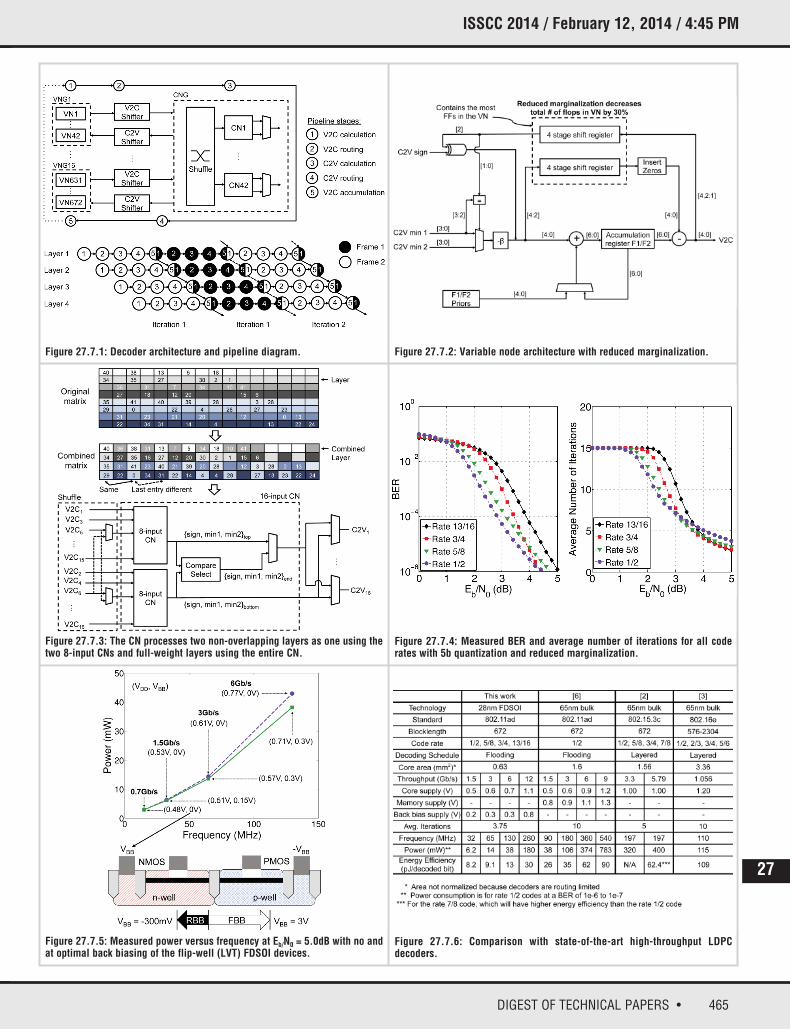
Figure 27.7.1 shows the overall architecture of the LDPC decoder. The decoderfully parallelizes the variable nodes (VN), layer serializes the check nodes (CN),where a layer is a row of submatrices, and uses a five-bit quantization for allmessages [4]. The flooding decoding schedule optimally utilizes the five-stagepipeline, and pipeline bubbles are eliminated by processing two subsequentframes simultaneously (Fig. 27.7.1). This deep pipelining shortens critical pathsand permits aggressive voltage and frequency scaling, which allows the powerto scale with throughput. To eliminate the need for an additional supply beyondthe core and back-bias supplies, the decoder uses flip-flop-based memory. Forthe size of the memories required by the decoder, the flip-flops at a scaled volt-age can have comparable efficiency to SRAM or eDRAM that must run on highersupply voltages. In addition, flip-flop-based designs transition well to new technologies in terms of reliability and time to market.
Memory dominates the power consumption of LDPC decoders, and the VNs (Fig.27.7.2) and pipeline registers comprise a majority of this decoder’s memory. Thenumber of pipeline stages and the number of registers per stage has been optimized for power during the architecture exploration phase [4]. The largestnumber of flip-flops within the VN is contained in the shift registers that storecheck-to-variable (C2V) and variable-to-check (V2C) messages for marginalization of incoming or outgoing messages. Reducing the number of bitsin these two blocks has a large effect on the total power since this architecturehas 672 VNs. To ensure that this does not significantly affect the error-correctingperformance of the decoder and to find the bits that should be removed, extensive simulations were performed where subsets of stored message bitswere used for marginalization. The simulations showed that two bits of precisioncould be removed from both the V2C and C2V shift registers with less than0.1dB loss in BER performance. From the C2V stored messages, the two leastsignificant bits are removed, and from the V2C stored messages, the least significant and the most significant magnitude bits are removed. The loss in performance can be recovered by increasing the maximum number of iterationsby 5, which increases the average number of iterations by less than 1% at Eb/N0
values of interest. This decreases the decoder’s power by 15% based on place-and-route results, and this technique can be applied to many LDPCdecoder architectures.
Reconfigurable decoders can require more cycles to decode lower rate codesdue to having more layers in the matrix, as well as longer critical paths fromextra hardware for flexible routing. A low-overhead method for reconfigurationis a key requirement to minimize power. This is accomplished for each of the 4codes defined in the standard by making the CNs switchable between acting asone 16-input CN to process a full-weight layer, or two 8-input CNs to processtwo half-weight layers. This switching is enabled by the non-overlapping layer
structure of the lower rate IEEE 802.11ad codes (Fig. 27.7.3). It allows all coderates to be processed in the same number of cycles, but it requires an extra stepof routing messages before and after the CNs. When non-overlapping layers areprocessed, the shuffler before the CN ensures that messages from the upperlayer are routed to the top 8 inputs of the CN, and those from the lower layer arerouted to the bottom 8 inputs. The multiplexers after the CN select the correctoutputs to send to the VNs, which depends on whether the VN is in the upper orlower layer. The shuffler can be simplified significantly for the parity check matrices of interest (e.g. as compared to [4]) by observing, firstly, that a CNdoes not need a specific ordering of its inputs if it is acting as a 16-input CN, andsecondly, that the interleaving pattern of the combined layers is nearly the samefor each combined layer for all code rates (Fig. 27.7.3). Using these insights,much of the routing is accomplished by shuffling fixed wires, eliminating manyof the long, complex global routes and multiplexers required in [4]. Since thepath from the output of the VNs to the input of the CNs is the critical path in thearchitecture, this optimization allows additional voltage and frequency scaling toreduce overall power consumption and mitigate the overhead of reconfiguration.
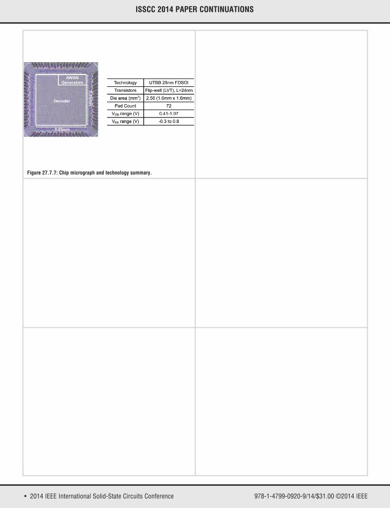
Figure 27.7.7 shows a micrograph of the LDPC decoder, which was fabricated ina 28nm UTBB FDSOI process. The chip is 0.85×0.85mm2, and the decoder corearea is 0.63mm2. It has four AWGN generators and an error collector in theperiphery that can be used to measure the BER, FER, and average number of iterations. An early termination block detects when the decoding result has satisfied all parity constraints and then ends decoding.
Figure 27.7.4 shows the BER performance and the average number of decodingiterations as a function of the channel conditions. The decoder achieves a BERof less than 10-6 in the waterfall region for all code rates defined in the standard.For a given BER level, the rate-1/2 code takes the most iterations to converge,taking, for example, an average of 3.75 iterations to converge at an Eb/N0 of5.0dB. For the rate-1/2 code at an Eb/N0 of 5.0dB and at the optimal core supplyvoltage, the decoder consumes 6.2mW, 14.4mW and 41mW for throughputs of1.5Gb/s, 3Gb/s and 6Gb/s, respectively. The power can be further decreased byusing the back biasing capability of the flip-well FDSOI devices (Fig. 27.7.5),which can implement LVT devices by biasing an n-well under NMOS devices anda p-well under PMOS devices [5]. This makes it possible to trade off leakage anddynamic power by adjusting the bias voltage on the n- and p-wells. Using opti-mal back bias and core supply voltages, the power can be decreased by 5.3%and 11% for the 3Gb/s and 6Gb/s throughputs, respectively (Fig. 27.7.5). Thereason for the moderate decrease in power is that the thresholds are alreadyclose to optimal for this application; however, if the throughput required is higher, the savings would be larger. The decoder has efficiencies of 8.2pJ/b,9.1pJ/b and 12.7pJ/b for the 1.5Gb/s, 3Gb/s and 6Gb/s throughputs. It consumes 3.0mW at a throughput of 0.7Gb/s at 15MHz with a core supply of0.48V and no back bias, and it consumes 179.9mW at a throughput of 12Gb/sat 260MHz with a core supply of 1.07V and a back bias voltage of 0.8V. Fig.27.7.6 compares this decoder to other state-of-the-art high-throughput decoderdesigns.
Acknowledgements:The authors thank the BWRC sponsors, STMicroelectronics for chip fabrication,A. Cathelin, P. Urard, A. Vladimirescu, V. Heinrich, A. Cevrero, Y. Leblebici, N. Preyss, J. Kwak, B. Zimmer, E. Yeo and Z. Zhang.
References:[1] T. Tsukizawa, et al., “A Fully Integrated 60GHz CMOS Transceiver ChipsetBased on WiGig/IEEE802.11ad with Built-In Self Calibration for MobileApplications,” ISSCC Dig. Tech. Papers, pp. 230-231, 2013.[2] S.W. Yen, et al., “A 5.79-Gb/s Energy-Efficient Multirate LDPC Codec Chip forIEEE 802.15.3c Applications,” IEEE J. Solid-State Circuits, vol.47, no.9, pp.2246-2257, 2012.[3] X. Peng, et al., “A 115mW 1Gbps QC-LDPC Decoder ASIC for WiMAX in65nm CMOS,” Asian Solid-State Circuits Conf., pp. 317-320, 2011.[4] M. Weiner, Z. Zhang, B. Nikolic, “LDPC Decoder Architecture for High-DataRate Personal-Area Networks,” IEEE International Symp. Circuits and Systems,pp. 1784–1787, 2011.[5] P. Flatresse, et al., “Ultra-Wide Body-Bias Range LDPC Decoder in 28nmUTBB FDSOI Technology,” ISSCC Dig. Tech. Papers, pp. 424-425, 2013.[6] Y. Park, et al., “A 1.6-mm2 38-mW 1.5-Gb/s LDPC Decoder Enabled byRefresh-Free Embedded DRAM,” IEEE Symp. VLSI Circuits, pp. 114-115, 2012.
978-1-4799-0920-9/14/$31.00 ©2014 IEEE
465DIGEST OF TECHNICAL PAPERS •
ISSCC 2014 / February 12, 2014 / 4:45 PM
Figure 27.7.1: Decoder architecture and pipeline diagram. Figure 27.7.2: Variable node architecture with reduced marginalization.
Figure 27.7.3: The CN processes two non-overlapping layers as one using thetwo 8-input CNs and full-weight layers using the entire CN.
Figure 27.7.5: Measured power versus frequency at Eb/N0 = 5.0dB with no andat optimal back biasing of the flip-well (LVT) FDSOI devices.
Figure 27.7.6: Comparison with state-of-the-art high-throughput LDPCdecoders.
Figure 27.7.4: Measured BER and average number of iterations for all coderates with 5b quantization and reduced marginalization.
27
• 2014 IEEE International Solid-State Circuits Conference 978-1-4799-0920-9/14/$31.00 ©2014 IEEE
ISSCC 2014 PAPER CONTINUATIONS
Figure 27.7.7: Chip micrograph and technology summary.