Irreversible Adsorption Controls Crystallization in …spikelab/papers/131.pdfIrreversible...
6
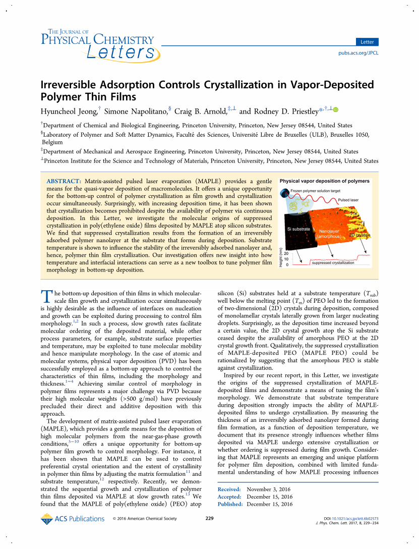
Irreversible Adsorption Controls Crystallization in Vapor-Deposited Polymer Thin Films Hyuncheol Jeong, † Simone Napolitano, § Craig B. Arnold, ‡,⊥ and Rodney D. Priestley* ,†,⊥ † Department of Chemical and Biological Engineering, Princeton University, Princeton, New Jersey 08544, United States § Laboratory of Polymer and Soft Matter Dynamics, Faculte ́ des Sciences, Universite ́ Libre de Bruxelles (ULB), Bruxelles 1050, Belgium ‡ Department of Mechanical and Aerospace Engineering, Princeton University, Princeton, New Jersey 08544, United States ⊥ Princeton Institute for the Science and Technology of Materials, Princeton University, Princeton, New Jersey 08544, United States ABSTRACT: Matrix-assisted pulsed laser evaporation (MAPLE) provides a gentle means for the quasi-vapor deposition of macromolecules. It offers a unique opportunity for the bottom-up control of polymer crystallization as film growth and crystallization occur simultaneously. Surprisingly, with increasing deposition time, it has been shown that crystallization becomes prohibited despite the availability of polymer via continuous deposition. In this Letter, we investigate the molecular origins of suppressed crystallization in poly(ethylene oxide) films deposited by MAPLE atop silicon substrates. We find that suppressed crystallization results from the formation of an irreversibly adsorbed polymer nanolayer at the substrate that forms during deposition. Substrate temperature is shown to influence the stability of the irreversibly adsorbed nanolayer and, hence, polymer thin film crystallization. Our investigation offers new insight into how temperature and interfacial interactions can serve as a new toolbox to tune polymer film morphology in bottom-up deposition. T he bottom-up deposition of thin films in which molecular- scale film growth and crystallization occur simultaneously is highly desirable as the influence of interfaces on nucleation and growth can be exploited during processing to control film morphology. 1,2 In such a process, slow growth rates facilitate molecular ordering of the deposited material, while other process parameters, for example, substrate surface properties and temperature, may be exploited to tune molecular mobility and hence manipulate morphology. In the case of atomic and molecular systems, physical vapor deposition (PVD) has been successfully employed as a bottom-up approach to control the characteristics of thin films, including the morphology and thickness. 1−4 Achieving similar control of morphology in polymer films represents a major challenge via PVD because their high molecular weights (>500 g/mol) have previously precluded their direct and additive deposition with this approach. The development of matrix-assisted pulsed laser evaporation (MAPLE), which provides a gentle means for the deposition of high molecular polymers from the near-gas-phase growth conditions, 5−10 offers a unique opportunity for bottom-up polymer film growth to control morphology. For instance, it has been shown that MAPLE can be used to control preferential crystal orientation and the extent of crystallinity in polymer thin films by adjusting the matrix formulation 11 and substrate temperature, 12 respectively. Recently, we demon- strated the sequential growth and crystallization of polymer thin films deposited via MAPLE at slow growth rates. 13 We found that the MAPLE of poly(ethylene oxide) (PEO) atop silicon (Si) substrates held at a substrate temperature (T sub ) well below the melting point (T m ) of PEO led to the formation of two-dimensional (2D) crystals during deposition, composed of monolamellar crystals laterally grown from larger nucleating droplets. Surprisingly, as the deposition time increased beyond a certain value, the 2D crystal growth atop the Si substrate ceased despite the availability of amorphous PEO at the 2D crystal growth front. Qualitatively, the suppressed crystallization of MAPLE-deposited PEO (MAPLE PEO) could be rationalized by suggesting that the amorphous PEO is stable against crystallization. Inspired by our recent report, in this Letter, we investigate the origins of the suppressed crystallization of MAPLE- deposited films and demonstrate a means of tuning the film’s morphology. We demonstrate that substrate temperature during deposition strongly impacts the ability of MAPLE- deposited films to undergo crystallization. By measuring the thickness of an irreversibly adsorbed nanolayer formed during film formation, as a function of deposition temperature, we document that its presence strongly influences whether films deposited via MAPLE undergo extensive crystallization or whether ordering is suppressed during film growth. Consider- ing that MAPLE represents an emerging and unique platform for polymer film deposition, combined with limited funda- mental understanding of how MAPLE processing influences Received: November 3, 2016 Accepted: December 15, 2016 Published: December 15, 2016 Letter pubs.acs.org/JPCL © 2016 American Chemical Society 229 DOI: 10.1021/acs.jpclett.6b02573 J. Phys. Chem. Lett. 2017, 8, 229−234
Transcript of Irreversible Adsorption Controls Crystallization in …spikelab/papers/131.pdfIrreversible...
Irreversible Adsorption Controls Crystallization in Vapor-DepositedPolymer Thin FilmsHyuncheol Jeong,† Simone Napolitano,§ Craig B. Arnold,‡,⊥ and Rodney D. Priestley*,†,⊥
†Department of Chemical and Biological Engineering, Princeton University, Princeton, New Jersey 08544, United States§Laboratory of Polymer and Soft Matter Dynamics, Faculte des Sciences, Universite Libre de Bruxelles (ULB), Bruxelles 1050,Belgium‡Department of Mechanical and Aerospace Engineering, Princeton University, Princeton, New Jersey 08544, United States⊥Princeton Institute for the Science and Technology of Materials, Princeton University, Princeton, New Jersey 08544, United States
ABSTRACT: Matrix-assisted pulsed laser evaporation (MAPLE) provides a gentlemeans for the quasi-vapor deposition of macromolecules. It offers a unique opportunityfor the bottom-up control of polymer crystallization as film growth and crystallizationoccur simultaneously. Surprisingly, with increasing deposition time, it has been shownthat crystallization becomes prohibited despite the availability of polymer via continuousdeposition. In this Letter, we investigate the molecular origins of suppressedcrystallization in poly(ethylene oxide) films deposited by MAPLE atop silicon substrates.We find that suppressed crystallization results from the formation of an irreversiblyadsorbed polymer nanolayer at the substrate that forms during deposition. Substratetemperature is shown to influence the stability of the irreversibly adsorbed nanolayer and,hence, polymer thin film crystallization. Our investigation offers new insight into howtemperature and interfacial interactions can serve as a new toolbox to tune polymer filmmorphology in bottom-up deposition.
The bottom-up deposition of thin films in which molecular-scale film growth and crystallization occur simultaneously
is highly desirable as the influence of interfaces on nucleationand growth can be exploited during processing to control filmmorphology.1,2 In such a process, slow growth rates facilitatemolecular ordering of the deposited material, while otherprocess parameters, for example, substrate surface propertiesand temperature, may be exploited to tune molecular mobilityand hence manipulate morphology. In the case of atomic andmolecular systems, physical vapor deposition (PVD) has beensuccessfully employed as a bottom-up approach to control thecharacteristics of thin films, including the morphology andthickness.1−4 Achieving similar control of morphology inpolymer films represents a major challenge via PVD becausetheir high molecular weights (>500 g/mol) have previouslyprecluded their direct and additive deposition with thisapproach.The development of matrix-assisted pulsed laser evaporation
(MAPLE), which provides a gentle means for the deposition ofhigh molecular polymers from the near-gas-phase growthconditions,5−10 offers a unique opportunity for bottom-uppolymer film growth to control morphology. For instance, ithas been shown that MAPLE can be used to controlpreferential crystal orientation and the extent of crystallinityin polymer thin films by adjusting the matrix formulation11 andsubstrate temperature,12 respectively. Recently, we demon-strated the sequential growth and crystallization of polymerthin films deposited via MAPLE at slow growth rates.13 Wefound that the MAPLE of poly(ethylene oxide) (PEO) atop
silicon (Si) substrates held at a substrate temperature (Tsub)well below the melting point (Tm) of PEO led to the formationof two-dimensional (2D) crystals during deposition, composedof monolamellar crystals laterally grown from larger nucleatingdroplets. Surprisingly, as the deposition time increased beyonda certain value, the 2D crystal growth atop the Si substrateceased despite the availability of amorphous PEO at the 2Dcrystal growth front. Qualitatively, the suppressed crystallizationof MAPLE-deposited PEO (MAPLE PEO) could berationalized by suggesting that the amorphous PEO is stableagainst crystallization.Inspired by our recent report, in this Letter, we investigate
the origins of the suppressed crystallization of MAPLE-deposited films and demonstrate a means of tuning the film’smorphology. We demonstrate that substrate temperatureduring deposition strongly impacts the ability of MAPLE-deposited films to undergo crystallization. By measuring thethickness of an irreversibly adsorbed nanolayer formed duringfilm formation, as a function of deposition temperature, wedocument that its presence strongly influences whether filmsdeposited via MAPLE undergo extensive crystallization orwhether ordering is suppressed during film growth. Consider-ing that MAPLE represents an emerging and unique platformfor polymer film deposition, combined with limited funda-mental understanding of how MAPLE processing influences
Received: November 3, 2016Accepted: December 15, 2016Published: December 15, 2016
Letter
pubs.acs.org/JPCL
© 2016 American Chemical Society 229 DOI: 10.1021/acs.jpclett.6b02573J. Phys. Chem. Lett. 2017, 8, 229−234

morphology, this investigation offers new insight into howsubstrate temperature and interfacial interactions can serve as anew toolbox to tune film morphology.Conceptually, MAPLE proceeds by the additive deposition of
a size distribution of polymer droplets.14 In the case of PEOdeposited atop Si, the larger droplets self-nucleate and act ascenters for dendritic 2D crystal growth. Smaller droplets eithercrystallize into 2D crystals via epitaxial growth from the nucleior spread atop the surface and remain amorphous, forming anamorphous nanolayer.13 While this mechanism is remarkablysimilar to the crystallization of metals and molecularcompounds deposited via PVD,4,15 the resulting morphologiesof the monolayers are in stark contrast due to suppressedcrystallization in the nanolayer that remains amorphous inMAPLE PEO films.To understand the origins of the suppressed crystallization in
MAPLE PEO films, we began by investigating the growth of 2Dcrystals from droplets of diameter D > 2.5 μm (microdroplets)as a function of deposition time (tdep). We conducted threesequential MAPLE depositions (M1, M2, and M3), each with 2h intervals at Tsub = 25 °C, on the same film and analyzed themorphology of the microdroplets formed at each time interval.The crystalline microdroplets exhibited two types ofmorphologies: type I, in which the crystalline droplet issurround by 2D crystals, or type II, in which the crystallinedroplet is surround by an amorphous nanolayer. The tworepresentative crystalline microdroplet morphologies areimaged by AFM in Figure 1a,b, respectively, and illustratedschematically in Figure 1c.Table 1 presents an analysis of the crystalline microdroplet
morphology at the three different time intervals, M1, M2, andM3. For tdep = 0−2 h, that is, during M1, 96% of the crystallinedroplets formed exhibited a type I morphology, while for tdep =2−4 h, that is, during M2, 75% of the crystalline dropletsformed exhibited a type I morphology. Strikingly, for tdep = 4−6h, that is, during M3, 0% of the crystalline droplets formedexhibited type I morphology. This interval-resolved morphol-
ogy analysis revealed several important observations: (i) nearlyall nucleating microdroplets initiated 2D crystal growth in theearly stages of film formation, and (ii) as tdep increased, theability of the nucleating droplets to initiate 2D crystal growthdiminished.As tdep increased, so did the thickness of the amorphous
nanolayer on the substrate, with a growth rate of ∼1.5 nm/h.Hence, while the crystalline microdroplets formed during M1were deposited atop a nanolayer of thickness 0−3 nm, thoseformed during M3 were deposited atop a nanolayer of thickness6−9 nm. In considering this difference, we argue that thepresence of a thick underlying PEO nanolayer prevents themicrodroplets from nucleating 2D crystals during the laterstages of film growth and, thus, suppresses the overallcrystallization. This is an important observation as it hints toa possible fundamental limitation in the gas-phase deposition ofmacromolecules.Furthermore, we analyzed whether 2D crystals formed
during M1 exhibited additional growth due the continueddeposition of PEO during later deposition intervals. Figure 1d,ecompares the morphology of the same 2D crystalline islandafter M1 and M2, respectively, showing the growth of 2Dcrystals during M2. As shown in Table 1, of the 2D crystallineislands formed during M1, only 62% exhibited additional 2D
Figure 1. (a,b) AFM amplitude images showing two types of crystalline microdroplets deposited during MAPLE at Tsub = 25 °C. (a) Type Imicrodroplet with surrounding 2D crystals; (b) type II microdroplet without 2D crystals. (c) Schematic showing the structure of type I and IIdroplets. (d,e) Optical microscopy images taken with a 405 nm laser showing the growth of 2D crystals after additive PEO deposition; (d) takenafter the first 2 h of MAPLE at Tsub = 25 °C (M1) and (e) taken after another 2 h of the second MAPLE (M2). (f) AFM height image showing themorphology of the MAPLE PEO film formed with tdep = 6 h (upper panel) and the corresponding AFM height profile (lower panel). Dendritic 2Dcrystals, a surrounding nanolayer, and an area scraped with a razor blade (Si surface) are depicted. No depletion zone exists between the 2D crystalgrowth front and the contacting nanolayer.
Table 1. Analysis of the Morphology of CrystallineMicrodroplets (D > 2.5 μm) and 2D Growth during ThreeSequential MAPLE (MP) Depositionsa
droplets of interestfirstMP
secondMP
thirdMP
type I droplets among crystalline droplets 0.96 0.75 0first MP crystalline droplets with 2Dgrowth
n/a 0.62 0
aThe first row shows the ratio of type I droplets among all crystallinedroplets formed at each different deposition. The second row showsthe ratio of the first MP crystalline droplets that developed detectable2D growth (> 2.5 μm) at the second and third MPs.
The Journal of Physical Chemistry Letters Letter
DOI: 10.1021/acs.jpclett.6b02573J. Phys. Chem. Lett. 2017, 8, 229−234
230

growth during M2, and no additional growth was exhibitedduring M3. In this case, the lateral faces as well as the foldsurfaces of the 2D crystals were surrounded by an amorphousnanolayer with no evidence of a depletion zone at the crystalgrowth front, as illustrated in Figure 1f. Remarkably, theamorphous PEO in direct contact with the crystal surface isstable against crystallization. These findings further illustratethe suppressed growth of 2D crystals as tdep increases. Moreimportantly, they corroborate the idea that as the thickness ofthe amorphous PEO nanolayer grows, with increasing tdep,growth of 2D crystals is suppressed.To investigate the long-term stability of the nanolayer against
crystallization, we monitored the morphology of a PEO film,deposited at Tsub = 25 °C atop Si, during aging. Figure 2a showsthe representative AFM morphology of the film directly after 3h of deposition at 25 °C in which both 2D crystals and ananolayer are present. The ∼10 nm thick 2D crystals, formed atan early stage of deposition, are covered with a ∼3 nm PEOnanolayer deposited afterward. The nanolayer atop the Si,which contacts with the lateral faces of the 2D crystals, isapproximately 5 nm thick. Figure 2b shows an AFM profileimage that confirms these film dimensions. We aged the filmunder N2 at 25 °C for 27 days to determine if the morphologyevolved with time. More specifically, we wanted to determinewhether amorphous PEO in the nanolayer transformed into the
crystalline phase from the lateral faces of the 2D crystals(primary growth, see Figure 2c) or from the top of the 2Dcrystals (secondary growth, see Figure 2c), both of which areexpected from an epitaxial growth mechanism.16−19 Surpris-ingly, the film morphology taken after 27 days of aging (seeFigure 2d) indicates that the 2D crystals showed no evidence ofprimary growth from the nanolayer at the Si interface (substratenanolayer) during the prolonged annealing period well belowTm. In essence, the substrate nanolayer is stable againstcrystallization and therefore does not allow for the growth of2D crystals in lateral dimensions. In contrast, evidence ofsecondary growth from the nanolayer atop 2D crystals (topnanolayer) was observed to a limited extent, as illustrated bythe dotted circles (SC1−3) in Figure 2d. Figure 2e shows anAFM height and profile image of a crystal SC1 in Figure 2d,formed by a secondary growth event. Thus, while the substratenanolayer at Si has no mobility for further crystallization, thenanolayer atop the 2D crystals had sufficient mobility forcrystallization.To better understand the origins of the suppressed
crystallization, we focused on obtaining evidence of strongPEO nanolayer−substrate interactions. Suppressed crystalgrowth in thin films has been associated with reductions ofthe mobility of chains in the uncrystallized fraction.20,21 In thinamorphous polymer films, such reduction of chain mobility can
Figure 2. (a) AFM height image of an as-deposited MAPLE PEO film made with Tsub = 25 °C and tdep = 3 h. (b) AFM height profile of the MAPLEPEO film in panel (a). The profile depicts ∼9.2 nm thick 2D crystals, a ∼3 nm top nanolayer deposited atop the 2D crystals, and a ∼5 nm substratenanolayer atop the Si surface. (c) Schematic showing two possible cases of 2D crystal growth in MAPLE PEO films upon aging. The blue arrowdescribes primary growth, continuing from the lateral faces of 2D crystals. The red arrow describes secondary growth, growing from the fold surfacesof the 2D crystals. (d) AFM height image of the film in panel (a) taken after 27 days of aging at 25 °C under a N2 environment. White dashed circlesdepict three secondary crystals (SC1−3) formed during aging. (e) AFM height image magnifying SC1 in panel (d) (upper panel) and thecorresponding height profile (lower panel).
Figure 3. AFM height image (a) and AFM profile (b) of a substrate nanolayer in a 3h@25C film, after 20 min of toluene washing. (c) Graphcomparing the nanolayer thickness in a 3h@25C film before and after toluene washing. AFM height image (d) and AFM profile (e) of a substratenanolayer in a 3h@50C film, after 20 min of toluene washing. (f) Graph comparing the substrate nanolayer thickness in a 3h@50C film before andafter toluene washing.
The Journal of Physical Chemistry Letters Letter
DOI: 10.1021/acs.jpclett.6b02573J. Phys. Chem. Lett. 2017, 8, 229−234
231

occur due to pinning of chain segments onto the substrate thatforms irreversibly adsorbed layers (IALs).22−24 We reason thatthe development of an IAL at the nanolayer−Si surfacesuppresses crystal growth. To establish the existence of an IAL,following Guiselin’s experiment,25−29 we measured the residualsubstrate nanolayer thickness after solvent washing of aMAPLE PEO film formed with Tsub = 25 °C and tdep = 3 h,that is, 3h@25C MAPLE. The methodology is a well-established technique to uncover loosely adsorbed chains inpolymer films; therefore, residual film thickness can be theindicator of the degree of adsorption. Solvent washing wasdone by dipping the films into toluene for 20 min. Figure 3a,bshows an AFM height image and a representative AFM profileof a residual substrate nanolayer after solvent washing,respectively. Figure 3c compares the average substrate nano-layer thickness before and after solvent washing. Clearly,solvent washing did not modify the original thickness (∼5 nm),thus indicating the presence of a strongly bound IAL.As the mobility of polymer chains critically depends on
temperature, we next sought to investigate the effect of a higherTsub close to Tm, at which the deposited PEO chains wouldhave a higher kinetic energy and thus higher desorptionprobability. We therefore deposited a PEO film at Tsub = 50 °Cfor tdep = 3 h, that is, 3h@50C MAPLE. Solvent washing wasperformed for 20 min after equilibrating the as-deposited 3h@50C sample at 25 °C for 5 min. Figure 3d,e shows an AFMheight image and a representative AFM profile of a solvent-washed residual substrate nanolayer, respectively, and Figure 3dcompares the average substrate nanolayer thickness before andafter solvent washing. Noticeably, the film thickness dramati-cally decreased from ∼5 to ∼1 nm after solvent washing. Asshown by the profile spectrum in Figure 3e, we can firmlyconclude that deposition at higher Tsub reduces the develop-ment of an IAL during MAPLE.On the basis of these findings, we next evaluated the
morphological development of the 3h@50C MAPLE PEO filmduring aging. The as-deposited 3h@50C sample was readilytransferred to the 25 °C temperature stage and monitoredunder optical microscopy to provide the same aging environ-ment as that in the case of the 3h@25C sample above. As thishigh Tsub (50 °C) effectively suppresses crystal nucleation ofPEO, the majority of the film would remain uncrystallizedduring deposition and only become able to nucleate whenmoved onto the 25 °C stage.13 Figure 4a compares a film
morphology right after crystallization of the N1 droplet (see theupper panel) at 25 °C and the morphology of the same regioncaptured after 1 h (see the lower panel). It is obvious that thecrystal growth propagated through the nanolayer region,forming dendritic 2D crystals. Such crystal growth propagatedinto the entire substrate region of ∼2 cm2 once nucleationevents occurred. Figure 4b is an optical microscopy image ofthe sample in Figure 4a, with time contours showing thelocation of the crystal growth front at times 0 (yellow line), 0.5(blue), 1 (red), and 4 min (black). The propagation of the 2Dgrowth crystallized microdroplets N1−N4 in the order named.Figure 4c plots the 2D crystal growth from the fourmicrodroplets in Figure 4b, N1−N4 respectively, as a functionof time. In the respective growth plots, the time ofcrystallization of the corresponding droplets was set to zero.They all collapsed in one line, indicated as a black dashed curve,showing retarded growth rate as they grow farther away fromthe microdroplet. Finally, Figure 4d exhibits the AFMmorphology of 2D crystals of the 3h@50C sample aftercrystallization. The ∼10 nm thickness of the 2D crystals isidentical to the thickness of the crystals formed via MAPLE atTsub = 25 °C.Interestingly, MAPLE deposition at Tsub = 50 °C renders
primary growth from the ∼5 nm thick nanolayer at 25 °C, asopposed to the case of the nanolayer with comparable thicknessand aging temperature but formed at Tsub = 25 °C. The findingscorroborate the notion that suppressed crystallization duringMAPLE is due to the development of an IAL during deposition.Irreversible adsorption of chains can lead to a reduction orcomplete suppression of crystallization as there is a highentropic barrier required for reorganization of chains fromIAL.21,30 From this point of view, we conclude that while thestrongly bound substrate nanolayer of ∼5 nm in 3h@25Csamples prohibits primary growth, the loosely adsorbednanolayer in 3h@50C allows the growth of primary MLCsonce nucleation events occur.In summary, we investigated crystal growth in vapor-
deposited PEO films and provided evidence that the depositiontemperature in MAPLE of polymers can affect the stability ofdeposited polymer thin films against crystallization. In a PEOfilm deposited at 25 °C, the uncrystallized fraction of the PEOwas strongly adsorbed to the Si surface and resistant tocrystallization during 25 °C aging. However, when thedeposition was performed at 50 °C, the adsorption of the
Figure 4. (a) Optical microscopy images taken with a 405 nm laser showing 2D crystal growth from a MAPLE PEO film during aging at 25 °C. Thefilm was made with Tsub = 50 °C and tdep = 3 h and quickly transferred onto a 25 °C temperature stage. The upper panel was captured right aftercrystallization in droplet N1, and the lower panel was captured after 1 h of aging; (b) propagation of 2D crystal growth as a function of time. (c)Plots showing 2D crystal growth from four microdroplets (N1−N4) in panel (b). The radial 2D crystal growth from each droplet is plotted as afunction of time elapsed from the point of droplet crystallization. (d) AFM height image (upper panel) showing 2D crystals grown from thesubstrate nanolayer during aging. The left side of the film was scraped with a razor blade. The measured height of the 2D crystals was ∼10 nm, asdepicted in the lower panel.
The Journal of Physical Chemistry Letters Letter
DOI: 10.1021/acs.jpclett.6b02573J. Phys. Chem. Lett. 2017, 8, 229−234
232

uncrystallized PEO fraction to Si was dramatically lessened andexhibited rapid crystal growth during 25 °C aging. Our resultsimply that the deposition temperature combined withinterfacial interactions can define the nature of deposited thinpolymer films in MAPLE processing, and the thermal history ofpolymer thin films can affect the crystallization kinetics. Futurework will seek to demonstrate how MAPLE deposition atopsubstrates with different properties can be used to control thinfilm morphology.
■ EXPERIMENTAL METHODSDetails of the MAPLE deposition of PEO were described in ourprevious study.13 The deposition of PEO (Mn = 4600 g/mol,polydispersity = 1.1) onto as-received Si substrates wasachieved by laser ablation from a frozen MAPLE target,where PEO was dissolved in dimethyl sulfoxide at aconcentration of 1 mg/mL. The laser ablation was conductedin a vacuum environment using a KrF laser (LightMachineryPulseMaster 844, λ = 248 nm, pulse duration = 20 ns). Thelaser was operated with a repetition rate of 5 Hz and energy of13.5−14.0 mJ/pulse with the focal area of 15 mm2.For solvent washing, the MAPLE PEO sample of interest was
cut into ∼0.5 cm × 2 cm sheets and then vertically soaked intoluene (20 mL volume glass vial) at room temperature. Aftersubmersion for 20 min, the sample was taken out, briefly rinsedwith fresh toluene, blown with N2, and dried in a vacuum ovenat room temperature. Three different regions of the film wereinvestigated via AFM to obtain the average thickness of asubstrate nanolayer before and after solvent washing.For AFM measurements, a tapping mode AFM (Asylum
Research MFP-3D-SA) was used for imaging. AFM imageprocessing and analysis were performed using Gwyddionsoftware. The thickness of a nanolayer in MAPLE PEO filmswas determined by measuring the height of steps obtained byremoving the MAPLE-deposited area with a razor blade. Onlyflat film areas having no microdroplets atop were considered inmeasuring the nanolayer thickness. The root-mean-squareroughness of a substrate nanolayer formed with 3 h ofMAPLE was typically below 1 nm.For optical microscopy measurements, a laser scanning
confocal microscope (Olympus OLS4000), equipped withwhite light and a 405 nm laser as a light source, was used forimaging. The images taken with the 405 nm laser wereprocessed to enhance contrast and brightness. A film area of∼1.53 × 105 μm2 was investigated for the analysis of 2D crystalgrowth as well as the morphology of crystalline microdropletsat each time interval of sequential MAPLE depositions (M1−M3).
■ AUTHOR INFORMATIONCorresponding Author*E-mail: [email protected] D. Priestley: 0000-0001-6765-2933NotesThe authors declare no competing financial interest.
■ ACKNOWLEDGMENTSR.D.P. and C.B.A. acknowledge support of the National ScienceFoundation (NSF) through a Materials Research Science andEngineering Center program through the Princeton Center forComplex Materials (DMR-1420541). R.D.P acknowledges the
support of the AFOSR through a PECASE Award (FA9550-12-1-0223). H.J. acknowledges support from the KwanjeongEducational Foundation in South Korea. S.N. acknowledgesfinancial support from the Fonds de la Recherche ScientifiqueFNRS under Grant No. T.0147.16 “TIACIC.”
■ REFERENCES(1) Zhang, Z.; Lagally, M. G. Atomistic Processes in the Early Stagesof Thin-Film Growth. Science 1997, 276, 377−383.(2) Barth, J. V.; Costantini, G.; Kern, K. Engineering Atomic andMolecular Nanostructures at Surfaces. Nature 2005, 437, 671−679.(3) Laudise, R. A.; Kloc, C.; Simpkins, P. G.; Siegrist, T. PhysicalVapor Growth of Organic Semiconductors. J. Cryst. Growth 1998, 187,449−454.(4) Meyer zu Heringdorf, F.-J.; Reuter, M. C.; Tromp, R. M. GrowthDynamics of Pentacene Thin Films. Nature 2001, 412, 517−520.(5) Pique, A.; McGill, R. A.; Chrisey, D. B.; Leonhardt, D.; Mslna, T.E.; Spargo, B. J.; Callahan, J. H.; Vachet, R. W.; Chung, R.; Bucaro, M.A. Growth of Organic Thin Films by the Matrix Assisted Pulsed LaserEvaporation (MAPLE) Technique. Thin Solid Films 1999, 355−356,536−541.(6) Chrisey, D. B.; Pique, A.; McGill, R. A.; Horwitz, J. S.; Ringeisen,B. R.; Bubb, D. M.; Wu, P. K. Laser Deposition of Polymer andBiomaterial Films. Chem. Rev. 2003, 103, 553−576.(7) Leveugle, E.; Zhigilei, L. V. Molecular Dynamics SimulationStudy of the Ejection and Transport of Polymer Molecules in Matrix-Assisted Pulsed Laser Evaporation. J. Appl. Phys. 2007, 102, 074914.(8) Guo, Y.; Morozov, A.; Schneider, D.; Chung, J. W.; Zhang, C.;Waldmann, M.; Yao, N.; Fytas, G.; Arnold, C. B.; Priestley, R. D.Ultrastable Nanostructured Polymer Glasses. Nat. Mater. 2012, 11,337−343.(9) Shepard, K. B.; Priestley, R. D. MAPLE Deposition ofMacromolecules. Macromol. Chem. Phys. 2013, 214, 862−872.(10) Ge, W.; Li, N. K.; McCormick, R. D.; Lichtenberg, E.; Yingling,Y. G.; Stiff-Roberts, A. D. Emulsion-Based RIR-MAPLE Deposition ofConjugated Polymers: Primary Solvent Effect and Its Implications onOrganic Solar Cell Performance. ACS Appl. Mater. Interfaces 2016, 8,19494−19506.(11) Liu, Y.; Atewologun, A.; Stiff-Roberts, A. D. OrganicSemiconductor Thin Films Deposited by Resonant Infrared Matrix-Assisted Pulsed Laser Evaporation: A Fundamental Study of theEmulsion Target. MRS Online Proc. Libr. 2014, 1733, 957.(12) Califano, V.; Bloisi, F.; Vicari, L.; Barra, M.; Cassinese, A.;Fanelli, E.; Buzio, R.; Valbusa, U.; Carella, A.; Roviello, A. SubstrateTemperature Dependence of the Structure of Polythiophene ThinFilms Obtained by Matrix Assisted Pulsed Laser Evaporation(MAPLE). Eur. Phys. J.: Appl. Phys. 2009, 48, 10505.(13) Jeong, H.; Shepard, K. B.; Purdum, G. E.; Guo, Y.; Loo, Y.-L.;Arnold, C. B.; Priestley, R. D. Additive Growth and Crystallization ofPolymer Films. Macromolecules 2016, 49, 2860−2867.(14) Shepard, K. B.; Arnold, C. B.; Priestley, R. D. Origins ofNanostructure in Amorphous Polymer Coatings via Matrix AssistedPulsed Laser Evaporation. Appl. Phys. Lett. 2013, 103, 123105.(15) Hwang, R.; Schroder, J.; Gunther, C.; Behm, R. Fractal Growthof Two-Dimensional Islands: Au on Ru(0001). Phys. Rev. Lett. 1991,67, 3279−3282.(16) Reiter, G.; Sommer, J.-U. Crystallization of Adsorbed PolymerMonolayers. Phys. Rev. Lett. 1998, 80, 3771−3774.(17) Reiter, G. Some Unique Features of Polymer Crystallisation.Chem. Soc. Rev. 2014, 43, 2055−2065.(18) Zhu, D.-S.; Liu, Y.-X.; Chen, E.-Q.; Li, M.; Chen, C.; Sun, Y.-H.;Shi, A.-C.; Van Horn, R. M.; Cheng, S. Z. D. Crystal GrowthMechanism Changes in Pseudo-Dewetted Poly(ethylene Oxide) ThinLayers. Macromolecules 2007, 40, 1570−1578.(19) Zhang, H.; Yu, M.; Zhang, B.; Reiter, R.; Vielhauer, M.;Mulhaupt, R.; Xu, J.; Reiter, G. Correlating Polymer Crystals via Self-Induced Nucleation. Phys. Rev. Lett. 2014, 112, 237801.
The Journal of Physical Chemistry Letters Letter
DOI: 10.1021/acs.jpclett.6b02573J. Phys. Chem. Lett. 2017, 8, 229−234
233

(20) Dalnoki-Veress, K.; Forrest, J. A.; Massa, M. V.; Pratt, A.;Williams, A. Crystal Growth Rate in Ultrathin Films of Poly(ethyleneOxide). J. Polym. Sci., Part B: Polym. Phys. 2001, 39, 2615−2621.(21) Vanroy, B.; Wubbenhorst, M.; Napolitano, S. Crystallization ofThin Polymer Layers Confined between Two Adsorbing Walls. ACSMacro Lett. 2013, 2, 168−172.(22) Koga, T.; Li, C.; Endoh, M. K.; Koo, J.; Rafailovich, M.;Narayanan, S.; Lee, D. R.; Lurio, L. B.; Sinha, S. K. Reduced Viscosityof the Free Surface in Entangled Polymer Melt Films. Phys. Rev. Lett.2010, 104, 066101.(23) Koga, T.; Jiang, N.; Gin, P.; Endoh, M. K.; Narayanan, S.; Lurio,L. B.; Sinha, S. K. Impact of an Irreversibly Adsorbed Layer on LocalViscosity of Nanoconfined Polymer Melts. Phys. Rev. Lett. 2011, 107,225901.(24) Jiang, N.; Sendogdular, L.; Di, X.; Sen, M.; Gin, P.; Endoh, M.K.; Koga, T.; Akgun, B.; Dimitriou, M.; Satija, S. Effect of CO2 on aMobility Gradient of Polymer Chains near an Impenetrable Solid.Macromolecules 2015, 48, 1795−1803.(25) Guiselin, O. Irreversible Adsorption of a Concentrated PolymerSolution. Europhys. Lett. 1992, 17, 225−230.(26) Fujii, Y.; Yang, Z.; Leach, J.; Atarashi, H.; Tanaka, K.; Tsui, O. K.C. Affinity of Polystyrene Films to Hydrogen-Passivated Silicon and ItsRelevance to the Tg of the Films. Macromolecules 2009, 42, 7418−7422.(27) Napolitano, S.; Wubbenhorst, M. The Lifetime of theDeviations from Bulk Behaviour in Polymers Confined at theNanoscale. Nat. Commun. 2011, 2, 260.(28) Gin, P.; Jiang, N.; Liang, C.; Taniguchi, T.; Akgun, B.; Satija, S.K.; Endoh, M. K.; Koga, T. Revealed Architectures of AdsorbedPolymer Chains at Solid-Polymer Melt Interfaces. Phys. Rev. Lett.2012, 109, 265501.(29) Bal, J. K.; Beuvier, T.; Unni, A. B.; Chavez Panduro, E. A.;Vignaud, G.; Delorme, N.; Chebil, M. S.; Grohens, Y.; Gibaud, A.Stability of Polymer Ultrathin Films (<7 nm) Made by a Top-DownApproach. ACS Nano 2015, 9, 8184−8193.(30) Martínez-Tong, D. E.; Vanroy, B.; Wubbenhorst, M.; Nogales,A.; Napolitano, S. Crystallization of Poly(L-lactide) Confined inUltrathin Films: Competition between Finite Size Effects andIrreversible Chain Adsorption. Macromolecules 2014, 47, 2354−2360.
The Journal of Physical Chemistry Letters Letter
DOI: 10.1021/acs.jpclett.6b02573J. Phys. Chem. Lett. 2017, 8, 229−234
234