Investigation on Leakage Loss in Multiple Via Row SIW ... · Investigation on Leakage Loss in...
8
International Journal of Scientific & Engineering Research, Volume 8, Issue ISSN 2229-5518 IJSER © 2017 http://www.ijser.org Investigation on Leakage Loss in Multiple Via Row SIW Structures Abdelrahman M. El-Akhdar, Ayman M. El-Tager, Hadia M. El-Hennawy Abstract—This paper presents a study of SIW based structures utilizing single via rows and multiple via rows with staggered via configuration. An expression to calculate the leakage ratio is deduced for the presented SIW structures utilizing double via row configuration. Moreover, parametric analysis is studied to relate other design parameters to the structure leakage ratio. Different case studies are introduced to obtain an optimized structure with certain via diameter, via pitch and row to row separation. The proposed configuration provides enhancement in the SIW power handling capability and operating bandwidth as well as a recognizable reduction in the insertion loss. To verify this approach, prototypes operating at the X-band are fabricated and measured. Measurements are in good agreement with simulations and calculations which verify the design approach as well as the paper outcomes. Index Terms— planar circuits, substrate integrated waveguides, transmission lines, leakage ratio, multiple via row, power handling capability, LTCC. —————————— —————————— 1 INTRODUCTION Ubstrate Integrated Waveguides based circuits using cy- lindrical via rows as the narrow wall boundaries of the conventional RWGs are widely used in multilayer microwave integrated circuits such as low-temperature co-fired ceramics (LTCC) and their applications in millimetric and terahertz fre- quencies [1]. They are used in many passive circuits such as: transmission lines [2], [3], filters [4-6], couplers [7-9], power dividers [10], [11] and active circuits [12], [13]. They combine the advantages of traditional rectangular waveguides such as high quality factor Q, low loss, and high power handling ca- pability to that of planar microstrip based circuits such as low cost, ease of fabrication, and the capability to be integrated with other devices. Many studies were adopted to analyze and calculate SIW design parameters. Full wave simulations are still required to analyse guided structures with different lengths [14]. A modification to the conventional boundary integral resonant mode expansion was presented in [15] to reduce the design parameters computational time. One of the crucial problems in SIW based circuits are the leakage oc- curred due to the periodic gaps existing between the cylindri- cal vias. SIW based structures leakage characteristics are ana- lysed and the modes of operation in single row configurations are studied in [16]. This paper provides efficient figure of mer- it to describe the leakage of SIW based structures utilizing double via row with staggered configuration shown in Figure 1. Double via rows with staggered configuration was previ- ously presented in [17-21] to provide low loss and to achieve high Q LTCC resonators. Moreover, double parallel via rows technique was presented in [22] to provide low loss LTCC cav- ity filter, but the staggered via rows provides lower loss. Therefore, double via rows with staggered configuration is investigated in detail throughout this paper with the objective of leakage reduction by prober choice of design parameters while maintaining high power handling capability. Fig 1. SIW structure using double via rows with staggered configuration This paper is organized as follows; Section 2 presents the de- sign parameters used in SIW based circuits utilizing double via rows with staggered configuration. Section 3 shows para- metric study for the proposed structure. Section 4 proposes simulations and design validation steps according to the de- duced analysis. Section 5 verifies the idea presented in this work by fabrication and measurements of six prototypes of SIW based TLs. Finally, Section 6 concludes the proposed work. 2 LEAKAGE OF SIW USING DOUBLE VIA ROW This section studies the SIW structure utilizing double via rows with staggered configuration shown in Figure 1 to end up with a definition of the leakage ratio of such structures. The structure design parameters are defined as follows: d …… via diameter P…… separation between two successive cylindrical vias a..……the physical width measured from the inner via rows aeff…… SIW effective width D……. distance between via rows in multiple row configura- tions. Figure 2 presents SIW based structure from the top view. The modes of operation n increase as the radiation angle θ decreas- es and the frequency decreases. The maximum leakage ap- S a D P d D 1381 IJSER
Transcript of Investigation on Leakage Loss in Multiple Via Row SIW ... · Investigation on Leakage Loss in...

International Journal of Scientific & Engineering Research, Volume 8, Issue ƗȮɯ,ÈÙÊÏɪƖƔƕƛɯɯɯ ISSN 2229-5518
IJSER © 2017 http://www.ijser.org
Investigation on Leakage Loss in Multiple Via Row SIW Structures
Abdelrahman M. El-Akhdar, Ayman M. El-Tager, Hadia M. El-Hennawy
Abstract—This paper presents a study of SIW based structures utilizing single via rows and multiple via rows with staggered via configuration. An expression to calculate the leakage ratio is deduced for the presented SIW structures utilizing double via row configuration. Moreover, parametric analysis is studied to relate other design parameters to the structure leakage ratio. Different case studies are introduced to obtain an optimized structure with certain via diameter, via pitch and row to row separation. The proposed configuration provides enhancement in the SIW power handling capability and operating bandwidth as well as a recognizable reduction in the insertion loss. To verify this approach, prototypes operating at the X-band are fabricated and measured. Measurements are in good agreement with simulations and calculations which verify the design approach as well as the paper outcomes.
Index Terms— planar circuits, substrate integrated waveguides, transmission lines, leakage ratio, multiple via row, power handling capability, LTCC.
—————————— ——————————
1 INTRODUCTION Ubstrate Integrated Waveguides based circuits using cy-lindrical via rows as the narrow wall boundaries of the
conventional RWGs are widely used in multilayer microwave integrated circuits such as low-temperature co-fired ceramics (LTCC) and their applications in millimetric and terahertz fre-quencies [1]. They are used in many passive circuits such as: transmission lines [2], [3], filters [4-6], couplers [7-9], power dividers [10], [11] and active circuits [12], [13]. They combine the advantages of traditional rectangular waveguides such as high quality factor Q, low loss, and high power handling ca-pability to that of planar microstrip based circuits such as low cost, ease of fabrication, and the capability to be integrated with other devices. Many studies were adopted to analyze and calculate SIW design parameters. Full wave simulations are still required to analyse guided structures with different lengths [14]. A modification to the conventional boundary integral resonant mode expansion was presented in [15] to reduce the design parameters computational time. One of the crucial problems in SIW based circuits are the leakage oc-curred due to the periodic gaps existing between the cylindri-cal vias. SIW based structures leakage characteristics are ana-lysed and the modes of operation in single row configurations are studied in [16]. This paper provides efficient figure of mer-it to describe the leakage of SIW based structures utilizing double via row with staggered configuration shown in Figure 1. Double via rows with staggered configuration was previ-ously presented in [17-21] to provide low loss and to achieve high Q LTCC resonators. Moreover, double parallel via rows technique was presented in [22] to provide low loss LTCC cav-ity filter, but the staggered via rows provides lower loss. Therefore, double via rows with staggered configuration is investigated in detail throughout this paper with the objective of leakage reduction by prober choice of design parameters while maintaining high power handling capability.
Fig 1. SIW structure using double via rows with staggered configuration This paper is organized as follows; Section 2 presents the de-sign parameters used in SIW based circuits utilizing double via rows with staggered configuration. Section 3 shows para-metric study for the proposed structure. Section 4 proposes simulations and design validation steps according to the de-duced analysis. Section 5 verifies the idea presented in this work by fabrication and measurements of six prototypes of SIW based TLs. Finally, Section 6 concludes the proposed work.
2 LEAKAGE OF SIW USING DOUBLE VIA ROW This section studies the SIW structure utilizing double via rows with staggered configuration shown in Figure 1 to end up with a definition of the leakage ratio of such structures. The structure design parameters are defined as follows: d …… via diameter P…… separation between two successive cylindrical vias a..……the physical width measured from the inner via rows aeff…… SIW effective width D……. distance between via rows in multiple row configura-tions. Figure 2 presents SIW based structure from the top view. The modes of operation n increase as the radiation angle θ decreas-es and the frequency decreases. The maximum leakage ap-
S
a
D
P
d
D
1381
IJSER

International Journal of Scientific & Engineering Research, Volume 8, Issue ƗȮɯ,ÈÙÊÏɪƖƔƕƛɯɯɯ ISSN 2229-5518
IJSER © 2017 http://www.ijser.org
pears in the smallest value θ as discussed in [16]. Using double via rows with staggered configuration shown in Figure 3 can reduce the electromagnetic waves leakage at the small values of radiation angle θ that reduces the overall circuit leakage. This section deduces an expression to determine the leakage ratio in SIW based structures utilizing double via rows with staggered configuration. Recalling the definition used to calculate the leakage ratio in single via row SIW based structures [16]. Assuming the elec-tromagnetic wave is travelling through the Z-direction as shown in Figure 2.
Fig 2. EM waves propagation through rectangular waveguide [16]
The reflection between the two sidewalls (TEn0) modes can be calculated according to the following relations [16]:
(1)
Figure 2 shows that as the frequency increases (wavelength decreases); the angle θ increases. While, as the mode order n increases; the angle θ decreases
Fig 3. Leakage propagation through the narrow wall of SIW structure Figure 3 presents the electromagnetic waves propagating
through the H-wall of double via row SIW structures. Vias in the inner and outer rows are staggered to reduce the leakage as possible. It is shown that an angle θ is illustrated as a func-tion of both the operating frequency and the mode of opera-tion as stated in Equation (1). Where, as the mode of opera-tion n increases, radiation angle θ decreases. This will lead to reflection from the staggered row and reduce the overall struc-ture leakage. A mathematical analysis is used to verify this method as follows:
The leakage part ratio occurred in single via row SIW based
circuit can be calculated using Equation (2) as presented in [16]:
(2)
Where, is the corresponding radiation angle to the cut off
frequency of the mode of operation and can be calculat-ed from the expression given in [1]. In this work, the leakage ratio is deduced for SIW based structures using double via rows with staggered configuration. The proposed expression can calculate the total leakage ratio presented in SIW structure shown in Figure 1.
(3)
Where;
RLeakage (total)…. is the total leakage occurred in the SIW structure using double via row. RLeakage (inner)…. is the leakage occurred due to the presence of the inner via row. RReturn (outer)…. is the returned electromagnetic waves according to the reflection from the outer via row.
Now, RLeakage (inner) can be calculated using the expression pre-sented in (2). While, RReturn (outer) is calculated using the follow-ing expression;
(4) And;
(5)
Note that: the radiation angle θouter in Equation (5) is calculated with respect to the distance between the inner and outer via rows D as stated in Equation (6).
(6)
Using the expressions from (1) to (6); Equation (3) can be re-written as:
(7)
(8)
(9)
———————————————— • Abdelrahman M. El-Akhdar is currently pursuing PhD degree in electrical
engineering in Ain Shams University, Egypt. E-mail: [email protected]
θ
aeff
X
Z
Wave Leakage
1382
IJSER

International Journal of Scientific & Engineering Research, Volume 8, Issue ƗȮɯ,ÈÙÊÏɪƖƔƕƛɯɯɯ ISSN 2229-5518
IJSER © 2017 http://www.ijser.org
Considering that the inner and the outer via rows are drilled using the same via diameter d and using the same separation between the two cascaded via cylinders P The expression pre-sented in (9) can be simplified as follows:
(10)
Using Equations (1) and (6) in Equation (10) we get;
(11)
It is fundamental that the operating mode n and the wave-
length λ are maintained across the whole structure. Then,
(12)
Where Equation (12) highlights the contribution presented
throughout this work. Equation (12) states that SIW based structures utilizing double via rows with staggered configura-tion reduce the overall leakage ratio. This interesting finding can be significant in multimode purpose, in such case as the radiation angle θ decreases the probability of leakage through the inner via row increases. But, for double via row configura-tion the probability of reflection and return due to the outer via rows increases leading to reduced leakage ratio of the overall structure. Relations connecting the previously defined design parameters are presented in the following sections.
3 PARAMETRIC STUDY OF SIW LEAKAGE To provide parametric analysis, six case studies are adopted throughout the paper. Case 1 and Case 2 shows SIW based structures using single via rows with the relations d/P equals to 0.5 and 0.25 respectively. While, Case studies 3, 4 and 5 shows the performance of SIW based structures using double via rows as follows: Case 3 has (P=2d, and D=2d), while Case 4 has (P=4d, and D=2d) and Case 5 has (P=4d, and D=4d). Moreover, an SIW based structure utilizing triple via rows is studied as Case 6, which has (P=4d, and D=4d). The previous section pre-sented the derivation of the leakage ratio occurred in SIW based circuits utilizing double via rows with staggered via configuration. This section presents a study on the design pa-rameters and their relations to provide SIW based structure with reduced loss. Equation (12) can be rewritten in terms of frequency as:
(13)
Where, c is the speed of light. Equation (13) is responsible for calculating the leakage ratio occurred in SIW based circuits utilizing double via rows in terms of via diameter d, separation between each two cascaded vias P, operating frequency f, mode of operation n, effective width aeff, and the distance be-tween the two via rows D. Therefore, the important parame-ters are studied as follows:
3.1 SIW effective Width An expression to calculate the effective width aeff of SIW based structures regarding to via diameter d and the separation be-tween cylindrical vias P is recalled from [16]:
(14) From Equation (14); the effective width aeff increases as the
separation between via rows P increases for a given width a and via diameter d. Figure 4 shows the relation between SIW based structures effective width aeff and the ratio between via diameter d to the separation between cylindrical vias P. The range of aeff described in Figure 4 is with respect to the feasible relations of the ratio d/P regarding to [14] and [22]. This rela-tion is related to a previous study stated that SIW structures can be realized from d <P<5d, otherwise posts are considered as a single inductor and not via wall waveguides [22]. So, SIW structures are valid for the ratio presented in Equations (15) and (16) which are the limits of Figure 4.
(15) Which leads to the following range for the ratio a/aeff
(16) But, the realization of the ratio d/P is limited to the fabrication fa-
cility which makes it tough to approach the upper limit 1.
Fig. 4. Relation of SIW via diameter and separation between cylindrical vias d/P versus SIW and corresponding RWG widths ratio a/aeff
The adopted 6 case studies can be categorized in 2 categories
with two different values of d/P. Category 1 includes Cases 1 and 3 (d/P=0.5). While Category 2 includes Cases 2, 4, 5 and 6 (d/P=0.25). These Case studies are plotted on the curve of Figure 4 within the lower part which is more realizable and agrees with what is pre-sented in [14, 16 and 22].
1383
IJSER

International Journal of Scientific & Engineering Research, Volume 8, Issue ƗȮɯ,ÈÙÊÏɪƖƔƕƛɯɯɯ ISSN 2229-5518
IJSER © 2017 http://www.ijser.org
3.2 Mode of Operation
In SIW based structures, circuit performance alters as the mode of operation n changes. This section studies the variation of the leak-age ratio RLeakage regarding to the operating mode n. From Equation (13), increasing the operating mode n leads to an increased overall circuit leakage. This expression is directly connected to Equation (1) and a previous study presented in [16]. This can be physically ex-plained as follows; as the mode of operation n increases, radiation angle θ decreases as shown in Figures 2 and 3. This is due to the reflections from both inner and outer via rows. Figure 5 shows a comparison between RLeakage for single via row Cases 1 and 2 and that of double via configurations Cases 3, 4, and 5 at different modes of operation n. It is clear from Figure 5 that the RLeakage in-creases as the mode of operation n increases. And RLeakage is reduced when using double via rows with staggered configuration. This indicates that the resulted leakage from the double row SIW will be less than that achieved by using conventional single via row SIW based circuits. In addition, it shows that Case 4 provides the lowest leakage case which will be verified by simulation and measure-ments of their insertion loss later.
1 2 3 4 50
0.1
0.2
0.3
0.4
0.5
0.6
0.7
0.8
0.9
Mode of operation
Leak
age
Rat
io
Single via row D=0Double via row D=2Double via row D=4
Fig. 5. Relation of the leakage ratio RLeakage with respect to the operating
modes nusing single and double via row configurations from Equation (13)
3.3 Operating Frequency Operating frequency is another important parameter in Equation
(13). This relation is introduced to study the relation between RLeakage and the operating frequency f. Figure 6 and Figure 7 show that RLeak-
age is less when using double via rows as Cases 3, 4 and 5 compared to that using single via row configuration as Cases 1 and 2. This can be explained by the much lower range of the leakage ratio in Figure 7 compared to that of Figure 6.
Fig. 6. Relation between the leakage ratio of SIW based structure using
single via row configurations with different separation between via rows P for various frequency points
Fig. 7. Relation between the leakage ratio of SIW based structure using
double via row configurations with different separation between via rows P for various frequencies
3.4 Power handling capability
An important advantage of SIW based structures is its high-power handling capability when compared to microstrip based circuits. The maximum power can be handled through conven-tional air-filled rectangular waveguide is presented in [25] using Equation (17). A more general expression used for dielectric filled rectangular waveguides and SIW based circuits is presented in [26] and rewritten in Equation (28). Figure 8 shows an added con-tour on the previous study [14]. The presented contour at P=4d shows the region providing enhanced power handling capability.
1384
IJSER

International Journal of Scientific & Engineering Research, Volume 8, Issue ƗȮɯ,ÈÙÊÏɪƖƔƕƛɯɯɯ ISSN 2229-5518
IJSER © 2017 http://www.ijser.org
Fig. 8. Region of SIW realization regarding to different relation between via diameter and separation between vias [14]
Equation (18) states that the maximum power Pmax increases as the effective width aeff increases. While, aeff increases when the rela-tion d/P decreases or when the separation between vias P increas-es for a given width a and via diameter d as shown in Equation (14) and Figure 4.
(17)
(18)
Where is the dielectric strength of the used substrate and h is the substrate thickness.
Figure 9 is plotted regarding to the expression presented in Equation (18) for SIW based structures where aeff varies according to the separation between vias which in our study takes only two values either P=2d for Cases 1 and 3 or P=4d for Cases 2, 4 ,5 and 6. Therefore, the 6 studied cases are plotted in only two points on the curve as shown in Figure 9. This agrees well with previous study presented in [16]. But, it is known that the relation P=4d suffers higher leakage if implemented using single via rows. Therefore, double via row with staggered configuration is good candidate for better leakage and enhanced power handling capa-bility.
In this section, all the parameters are studied regarding to their effect on the RLeakage of SIW based structures. It is shown that, RLeakage increases by increasing the separation between vias, but it is remarkably enhanced by using double via row with staggered configuration. Also, RLeakage increases as the mode n increases which also is enhanced by utilizing double via rows with the pre-sented configuration. Moreover, the relation between the radia-
tion angle θ and the operating frequency is directly proportional. As the frequency increases, the RLeakage increases.
Fig. 9. Calculated maximum power for the SIW based structures with sin-
gle and double via row configurations using Equation (18)
As a conclusion, Section 3 provides the designer with the im-portant considerations to achieve SIW based structure with re-duced losses regarding to the structure leakage ratio and high power handling capability. Next Section presents simulations ofthe selected six case studies to proof the proposed idea.
4 SIMULATIONS OF SELECTED CASE STUDIES
In this paper, 3D EM full-wave models are obtained using (CST) to validate both frequency and time domain simula-tions. A taper to microstrip line transition presented in [27] and [28] is used to provide transitions and port excitations. The six case studies of SIW based structures stated in Section 3 are simulated and fabricated. The 3D simulated models are presented in Figure 10.
(a) (b) (c) (d) (e) (f)
Fig. 10. 3D EM models of the proposed SIW Case studies (a) Case 1,
(b) Case 2, (c) Case 3, (d) Case 4, (e) Case 5, (f) Case 6.
1385
IJSER
International Journal of Scientific & Engineering Research, Volume 8, Issue ƗȮɯ,ÈÙÊÏɪƖƔƕƛɯɯɯ ISSN 2229-5518
IJSER © 2017 http://www.ijser.org
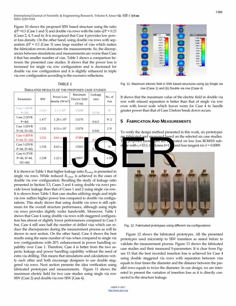
Figure 10 shows the proposed SIW based structure using the ratio d/P =0.5 (Case 1 and 3) and double via rows with the ratio d/P = 0.25 (Cases 2, 4, 5 and 6). It is recognized that Case 4 provides low pow-er loss density. On the other hand, using double via rows with sep-aration d/P = 0.5 (Case 3) uses large number of vias which makes the fabrication errors dominates the measurements. So, the discrep-ancies between simulations and measurements are worse than Case 4 that has smaller number of vias. Table 1 shows a comparison be-tween the presented case studies. It shows that the power loss is increased for single via row configuration and is decreased for double via row configuration and it is slightly enhanced in triple via row configuration according to the excessive reflections.
TABLE 1 SIMULATED RESULTS OF THE PROPOSED CASE STUDIES
Parameters BW Power Loss
density (W/m3)
Maximum Electric field
(V/m)
Leakage ratio
No. of vias
Case 1 (SVR P=2d)
1.513 1.1 x 10⁶ 15298 0.556
N
Case 2 (SVR P=4d)
1.477 1.28 x 10⁶ 13176 0.611
N /2
Case 3 (DVR P=2d, D=2d)
1.535 8.53 x 10⁵ 15378 0.042
2 N
Case 4 (DVR P=4d, D =2d)
1.531 8.61 x 10⁵ 17484 0.142
N
Case 5 (DVR P=4d, D=4d)
1.518 8.63 x 10⁵ 15503 0.178
N
Case 6 (TVR P=4d, D=4d,
D2=4d) 1.538 1.22 x 10⁶ 18897
- 1.5N
It is shown in Table 1 that higher leakage ratio RLeakage is presented in single via rows. While reduced RLeakage is achieved in the cases of double via row configuration. Recalling the study of leakage ratio presented in Section 3.3, Cases 3 and 4 using double via rows pro-vide lower leakage than that of Cases 1 and 2 using single via row. It is shown from Table 1 that case studies utilizing single and triple via row suffers higher power loss compared to double via configu-rations. This study shows that using double via rows is still opti-mum for the overall structure performance, although using triple via rows provides slightly wider bandwidth. Moreover, Table 1 shows that Case 4 using double via rows with staggered configura-tion has almost or slightly lower performances compared to Case 3 but, Case 4 still uses half the number of drilled vias which can re-duce the discrepancies during the measurement process as will be shown in next section. On the other hand, Case 4 shows the best results using the same number of vias when compared to single via row configurations with 20% enhancement in power handling ca-pability over Case 1. Therefore, Case 4 is better from the two as-pects; leakage and power handling capability without the need of extra via drilling. This means that simulations and calculations veri-fy each other and both encourage designers to use double stag-gered via rows. Next section presents the idea verification using fabricated prototypes and measurements. Figure 11 shows the maximum electric field for two case studies using single via row SIW (Case 2) and double via row SIW (Case 4).
Fig. 11. Maximum electric field in SIW based structures using (a) Single via row (Case 1) and (b) Double via row (Case 4)
It shows that the maximum value of the electric field in double via row with relaxed separation is better than that of single via row even with lower scale which leaves room for Case 4 to handle greater power than that of Case 2 before break down occurs.
5 FABRICATION AND MEASUREMENTS To verify the design method presented in this work, six prototypes are fabricated and measured based on the selected six case studies. The proposed prototypes are fabricated on low loss RO6010 sub-strate with ɛr=10.5, thickness h=1.25 and loss tangent tan δ = 0.0009.
Fig. 12. Fabricated prototypes using different via configurations Figure 12 shows the fabricated prototypes. All the presented
prototypes used microstrip to SIW transition as stated before to validate the measurement process. Figure 13 shows the fabricated case studies and their measured S-parameters. It is clear from Fig-ure 13 that the best recorded insertion loss is achieved for Case 4 using double staggered via rows with separation between vias equals to four times the diameter and the distance between the par-allel rows equals to twice the diameter. In our design, we are inter-ested to present the variation of insertion loss as it is directly con-nected to the structure leakage.
1386
IJSER

International Journal of Scientific & Engineering Research, Volume 8, Issue ƗȮɯ,ÈÙÊÏɪƖƔƕƛɯɯɯ ISSN 2229-5518
IJSER © 2017 http://www.ijser.org
Fig. 13. Simulated (Solid-line) versus measured (Dotted-line) S-
Parameters for the proposed case studies (Black line presents S21, Red line shows S11, and Blue line shows S22) (a)Case 1, (b) Case 2, (c) Case 3,
(d) Case 4, (e) Case 5, (f) Case 6. Figure 14 shows a comparison between the measured (S21) in dB for the proposed case studies.
Fig. 14. measured S12 in dB of the six prototypes
From Figure 14, using single via row with via separation P=2d (Case 1) provides medium insertion loss for a limited operational bandwidth. (Case 2) using single via row with P=4d shows the worst distorted IL according to the high leakage loss compared to other case studies as expected. On the other hand, (Case 3) that uses P=2d and D=2d shows low insertion loss but at limited bandwidth as (Case 1) which can be useless. Double via row (Case 4) using P=4d and D=2d shows the best performance of enhanced insertion loss for a broadband operating bandwidth without the need of drilling extra vias compared to the other Case studies. While (Case 5) uses double via rows with P=4d and D=4d provides enhanced
insertion loss, but it suffers from a transmission zero that could be vital in multi band operation. Finally, it is important to mention that using triple via rows with staggered configuration shown in Case 6 provides a lower fluctuating insertion loss compared to all other cases, but at the same time Case 4 presents the lowest insertion loss compared to all other cases including Case 3 which has better simu-lated IL. This is because utilizing double via rows with separation d/P = 0.5 (Case 3) uses large number of vias which makes the fabri-cation errors dominates the measurements. So, the discrepancies between simulations and measurements are worse than Case 4 that has smaller number of vias. As a conclusion, Table 2 summarizes the previous case studies.
TABLE 2 MEASUREMENTS OF PRESENTED CASE STUDIES
Case Studies/Parameters Insertion Loss(dB)
Operating Bandwidth
(GHz)
Calculated Leakage Ratio
Case 1 (SVR P=2d) 3.444 0.933 0.556 Case 2 (SVR P=4d) 3.165 0.803 0.611
Case 3 (DVR P=2d, D=2d) 2.034 2.365 0.042 Case 4 (DVR P=4d, D=2d) 1.945 2.757 0.142 Case 5 (DVR P=4d, D=4d) 2.17471 2.467 0.178 Case 6 (TVR P=4d, D=4d) 2.185 2.557 -
Enhancement (Case4 versus Case1)
43.52 % 66.15 % 74.46 %
From Table 2, SIW based structures utilizing double via rows pre-sented in this work (Case 4) could achieve better performance com-pared to the conventional SIW based structures (Case 1) in terms of both leakage and power handling capability without the need of extra via drilling. Moreover, Table 3 highlights the contribution presented in this paper compared to the conventional SIW based structure.
TABLE 3 COMPARISON BETWEEN SIW STRUCTURES
Case Studies/Parameters Conventional SIW (SVR P=2d, Case 1)
Best case in this Work (Case 4)
Enhancement
Leakage Ratio High Low 74.46 % Insertion Loss High Low 43.52 %
Power Loss density High Low 22.63 %
Number of drilled vias N N No extra via
drilling Operational bandwidth Low High 66.15 % Maximum Electric field High Low 11.82 %
6 CONCLUSION
This paper studies a practical configuration to enhance SIW based structures. The proposed structure is achieved by applying double via rows with staggered configuration instead of single via rows presented in conventional SIW structures. An expression to calcu-
1387
IJSER

International Journal of Scientific & Engineering Research, Volume 8, Issue ƗȮɯ,ÈÙÊÏɪƖƔƕƛɯɯɯ ISSN 2229-5518
IJSER © 2017 http://www.ijser.org
late a leakage ratio for SIW based structures using double via rows is deduced. A parametric study is done to provide relations be-tween the physical design parameters. The objective is to obtain the best structure in terms of both insertion loss and power handling capability. To verify the proposed idea, six prototypes operating at the X-band were fabricated and measured. The proposed structure recorded an enhanced performance compared to the conventional SIW based structures utilizing single via row. It is concluded that the best configurationis Case 4 using double staggered via rows with separation between vias equals to four times the via diameter and the distance between the parallel rows equals to twice the di-ameter. It achieves 43.52% enhancement in insertion loss and 66.15% wider bandwidth and about 74.46 % lower leakage ratio and 20% higher power handling capability when compared to con-ventional SIW structures utilizing single via rows using the same number of drilled vias. Measurements agree well with simulations and calculated results which verify the proposed design method.
REFERENCES [1] M. Bozzi, L. Perregrini, K. Wu, P. Arcioni “Current and future re-
search trends in substrate integrated waveguide technology.” Radio engineering, Vol.18, No.2, June 2009, pp. 201-209
[2] F. Parament, A. Ghiotto, T.-P. Voung, J. Duchamp, K. Wu, “Broad-band transition for dielectric filled to air filled substrate integrated waveguide for low loss and high power handling millimetre wave substrate integrated circuits.” IEEE-MTT-S International Microwave Symposium pp. 1-3,2014
[3] M. D. Sindrev, J. Bonache, F. Martin, T. Itoh, “Novel fully-planar extended composite right/left handed transmission line based on substrate integrated waveguide for multi-band applications.” Pro-ceeding of the 42nd European microwave conference. Pp. 578-581, 30 Oct-1 Nov. Amsterdam, The Netherlands, 2012.
[4] M. Salehi, J. Bornemann, E. Mehrshahi. “Compact folded substrate integrated waveguide Filter with non-resonanting nodes for high se-lectivity bandpass applications.” Proceeding of the 43rd European mi-crowave conference. Pp. 155-158, 7-10 Oct, Nuremburg, Germany, 2013.
[5] L. Huong, I. D. Robertson, N. Yuan. “Substrate integrated waveguide filters with face to face broadside coupled complementary split ring resonator.” Proceeding of the 43rd European microwave conference. Pp. 29-32, 7-10 Oct, Nuremburg, Germany, 2013.
[6] S. A. Shakib, V. Sekar, K. Entesari. “A compact triple band pass filter based on half-mode substrate integrated waveguides.” Proceeding of the 42nd European microwave conference. Pp. 116-119, 30 Oct-1 Nov. Amsterdam, The Netherlands, 2012.
[7] V. A. Labay, J. Bornemann, “Multilayered substrate integrated wave-guide couplers.” Workshop WSI: Substrate integrated circuits, IEEE-MTT-S International Microwave Symposium 2010.
[8] D. Dousset, J. Bornemann, M. Daigle, S. Cloude, K. Wu, “Broad-band 100 GHz substrate integrated waveguide couplers with irregularly shaped via holes for high order mode suppression.” Proceeding of the 42nd European microwave conference. Pp. 277-280, 30 Oct-1 Nov. Am-sterdam, The Netherlands, 2012.
[9] F. Parment, A. Ghiotto, T.- P. Voung, J. M. Dochamp, K. Wu, “Air-filled substrate integrated waveguide for low loss and high power handling millimetre wave substrate waveguide circuits.” IEEE Transactions on Microwave Theory and Techniques, vol. 63, Issue. 4, pp. 1228-1238, 2015
[10] Z. Kordiboujeni, J. Bornemann, “Efficient design of substrate inte-grated waveguide power dividers for antenna feed systems.” Europe-an conference for antenna and propagation (EuCAP), pp. 344-348, 2013.
[11] K. Kim, J. Byun, H. Y. Lee, “Substrate integrated waveguide Wil-kinson power divider with improved isolation performances.” Pro-gress in Electromagnetic Research Letters, Vol. 19, pp. 41-48. 2010.
[12] S. Sirci, J. D. Martinez, M. Tarancher, V. E. Boria, “Analog tuning of com-pact varactor loaded combline filters in substrate integrated waveguide.” Proceeding of the 42nd European microwave conference. Pp. 257-260, 30 Oct-1 Nov. Amsterdam, The Netherlands, 2012.
[13] S. Sirci, J. D. Martinez, V. E. Boria, “Low loss 3 bit tunable SIW filter with PIN diodes and integrated bias network.” Proceeding of the 43rd European microwave conference. Pp. 1211-1214, 7-10 Oct, Nuremburg, Germany, 2013.
[14] D. Deslands and K. Wu, "Accurate Modeling, Wave Mechanisms, and Design Considerations of a Substrate Integrated Waveguide," IEEE Transactions on Microwave Theory and Techniques, Vol. 54, No. 6, June 2006. Pp. 2516-2526.
[15] F. Mira, A.A. San Blasy, V.E. Boriaz and B. Gimenox “Fast and accu-rate analysis and design of SIW filters.” Proceeding of the 37th Europe-an microwave conference. Oct. Munich, Germany, Pp. 170-173. 2007.
[16] F. Xu and K. Wu, "Guided-wave and leakage characteristics of sub-strate integrated waveguide," IEEE Transactions on Microwave Theory and Techniques, vol. 53, pp. 66-73, Jan. 2005.
[17] A. M. Eltager, L. Roy, “Study of Cylindrical Multilayer Resonators with Rectangular Air cavity for Low Phase Noise K/Ka-Band oscilla-tors.” IEEE Transactions on Microwave Theory and Techniques, Vol. 53, No.6, pp.2211-2219, 2005.
[18] A. M. El-Tager and L. Roy, “High-Q LTCC resonators for millimeter- wave applications,” in IEEE MTT-S International Microwave Symposi-um, Digest, Jun. 2003, vol. 33, pp. 2257–2260.
[19] A. M. El-Tager and L. Roy, “Novel cylindrical high-Q LTCC resona-tors for millimeter-wave applications,” in IEEE MTT-S International Microwave Symposium Dig., Jun. 2004, vol. 3, pp. 637–640.
[20] D. Y. Jung, K. C. Eun, and C. S. Park, “High-Q Circular LTCC Reso-nator Using Zigzagged Via Posts and a λ/4 Short Stub for Millime-ter-Wave System-on-Package Applications.” IEEE Transaction on Mi-crowave Advanced packaging, Vol. 32, No. 1, Feb. 2009.
[21] A. El-Akhdar, H. El-Hennawy, A. El-Tager, “A Study on Double Via row Configuration for SIW based structures.” IEEE- International con-ference on Microelectronics ICM2016, Cairo, Egypt.
[22] J.-H. Lee, S. Pinel, J. Papapolymerou, J. Laskar, and M. M. Tentzeris. “Low Loss LTCC Cavity Filters Using System-on-Package Technolo-gy at 60 GHz.” IEEE Transaction on Microwave Theory and Techniques, Vol. 53, Issue 12, Dec. 2005.
[23] J.R. Bray and L. Roy, “Resonant frequencies of post-wall wave-guide,” Proceeding of IEE Microwave Antennas and Propagation, vol. 150, pp. 365–368, Oct. 2003.
[24] David M. Pozar “Microwave Engineering.” 4th Edition, Wiley. 2012. [25] R. E. Collin, “Foundations for Microwave Engineering,” McGraw-
Hill, International Edition, PP.340-351, 1966. [26] R. J. Cameron, Ch. M. Kudsia, R.R. Mansour, “Microwave filters for
Communication Systems.” Wiley-Interscience, 2007. [27] Y. J. Cheng, K. Wu, and W. Hong, “Power Handling Capability of
Substrate Integrated Waveguide Interconnects and Related Trans-mission Line Systems.” IEEE Transactions of Microwave Theory and Techniques, vol. 31, no. 4, pp. 900–909, Nov. 2008.
[28] D. Deslandes and K. Wu, “Integrated transition of coplanar to rec-tangular waveguides,” IEEE MTT-S International Microwave Symposi-um Digest, Feb. 2001, pp. 619–622.
[29] Dominic Deslandes, “Design Equations for Tapered Microstrip-to-Substrate Integrated Waveguide Transitions.” IEEE MTT-S Interna-tional Microwave Symposium Dig., 2010, pp.704–707.
1388
IJSER