
Investigation of a Voltage Probe in Microstrip Technology ...
53
Investigation of a Voltage Probe in Microstrip Technology (Specifically in 7-tesla MRI System) By : Mona ParsaMoghadam Supervisor : Prof. Dr. Ing- Klaus Solbach April 2015
Transcript of Investigation of a Voltage Probe in Microstrip Technology ...
Investigation of a Voltage Probe in Microstrip Technology
(Specifically in 7-tesla MRI System)
By : Mona ParsaMoghadam
Supervisor : Prof. Dr. Ing- Klaus Solbach
April 2015
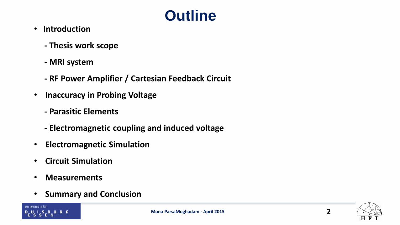
Outline
Mona ParsaMoghadam - April 2015 2
• Introduction
- Thesis work scope
- MRI system
- RF Power Amplifier / Cartesian Feedback Circuit
• Inaccuracy in Probing Voltage
- Parasitic Elements
- Electromagnetic coupling and induced voltage
• Electromagnetic Simulation
• Circuit Simulation
• Measurements
• Summary and Conclusion
Outline
Mona ParsaMoghadam - April 2015 3
• Introduction
- Thesis work scope
- MRI system
- RF Power Amplifier / Cartesian Feedback Circuit
• Inaccuracy in Probing Voltage
- Parasitic Elements
- Electromagnetic coupling and induced voltage
• Electromagnetic Simulation
• Circuit Simulation
• Measurements
• Summary and Conclusion
Thesis work scope
Mona ParsaMoghadam - April 2015 4
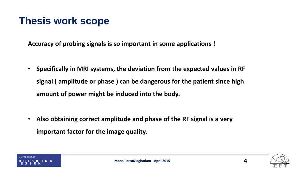
Accuracy of probing signals is so important in some applications !
• Specifically in MRI systems, the deviation from the expected values in RF
signal ( amplitude or phase ) can be dangerous for the patient since high
amount of power might be induced into the body.
• Also obtaining correct amplitude and phase of the RF signal is a very
important factor for the image quality.

Different Part of MRI System
Mona ParsaMoghadam - April 2015 5
• Magnet :
Producing a constant magnetic field (𝑩𝟎)
• Gradient Coil
Producing a ramp signal for 𝑩𝟎 magnetic field
• RF Coil
Generates 𝑩𝟏 field by time varying RF signal
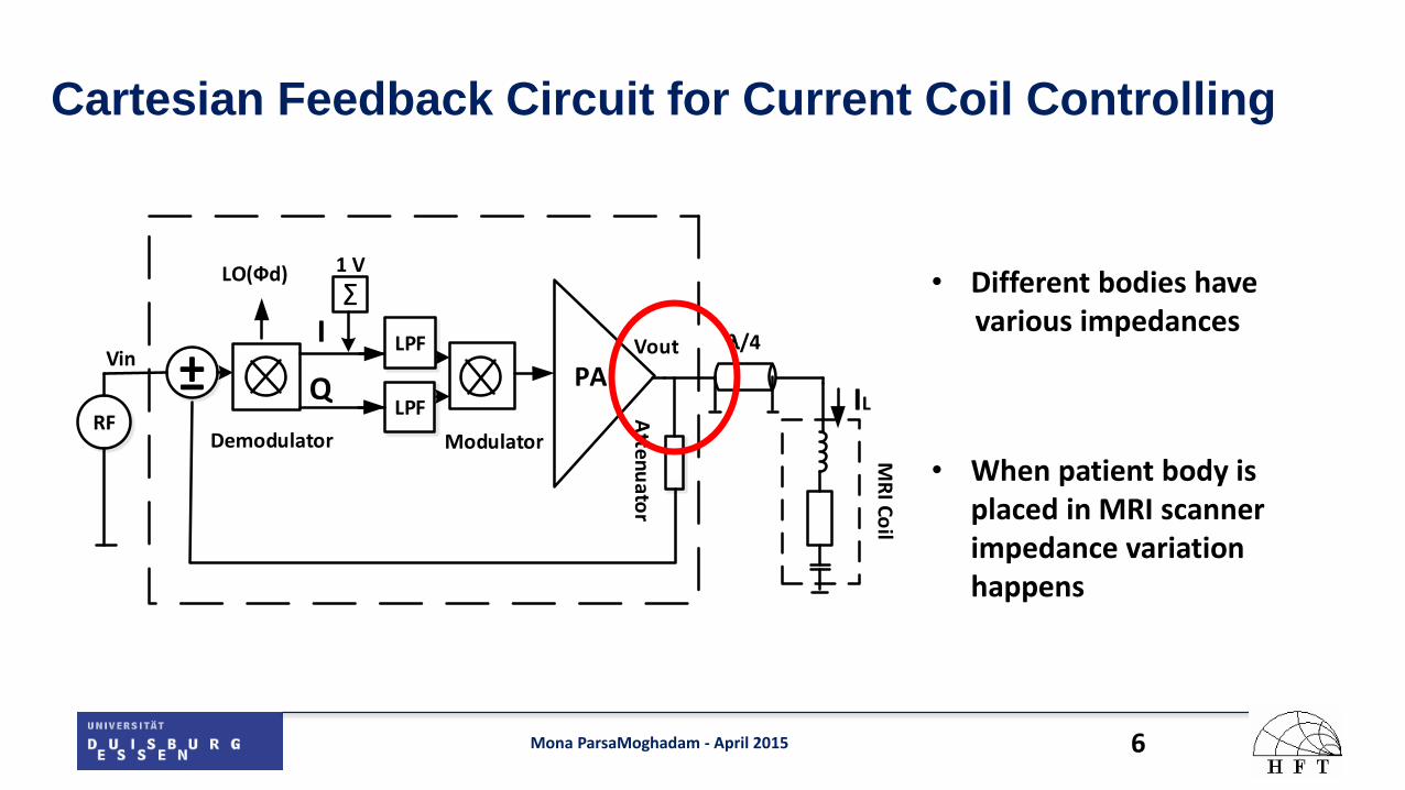
Cartesian Feedback Circuit for Current Coil Controlling
Mona ParsaMoghadam - April 2015 6
± RF
Demodulator Modulator
LO(Фd)
PA
Atte
nua
tor
MR
I Co
il
Q
LPF
LPF
IVin
Vout λ/4
IL
Σ 1 V
• Different bodies have various impedances
• When patient body is placed in MRI scanner impedance variation happens
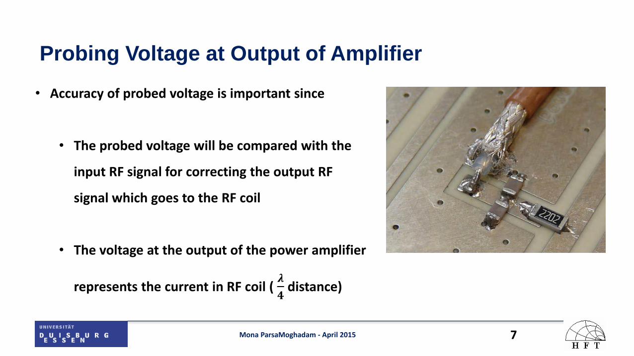
Probing Voltage at Output of Amplifier
Mona ParsaMoghadam - April 2015 7
• Accuracy of probed voltage is important since
• The probed voltage will be compared with the
input RF signal for correcting the output RF
signal which goes to the RF coil
• The voltage at the output of the power amplifier
represents the current in RF coil ( 𝝀
𝟒 distance)
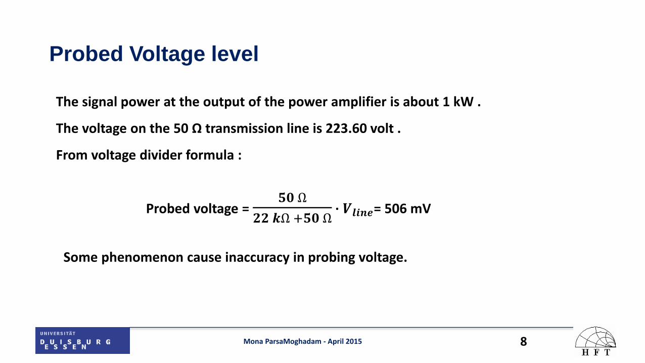
Probed Voltage level
Mona ParsaMoghadam - April 2015 8
The signal power at the output of the power amplifier is about 1 kW .
The voltage on the 50 Ω transmission line is 223.60 volt .
From voltage divider formula :
Probed voltage = 𝟓𝟎 Ω
𝟐𝟐 𝒌Ω +𝟓𝟎 Ω · 𝑽𝒍𝒊𝒏𝒆= 506 mV
Some phenomenon cause inaccuracy in probing voltage.
Outline
Mona ParsaMoghadam - April 2015 9
• Introduction
- Thesis work scope
- MRI system
- RF Power Amplifier / Cartesian Feedback Circuit
• Inaccuracy in Probing Voltage
- Parasitic Elements
- Electromagnetic coupling and induced voltage
• Electromagnetic Simulation
• Circuit Simulation
• Measurements
• Summary and Conclusion
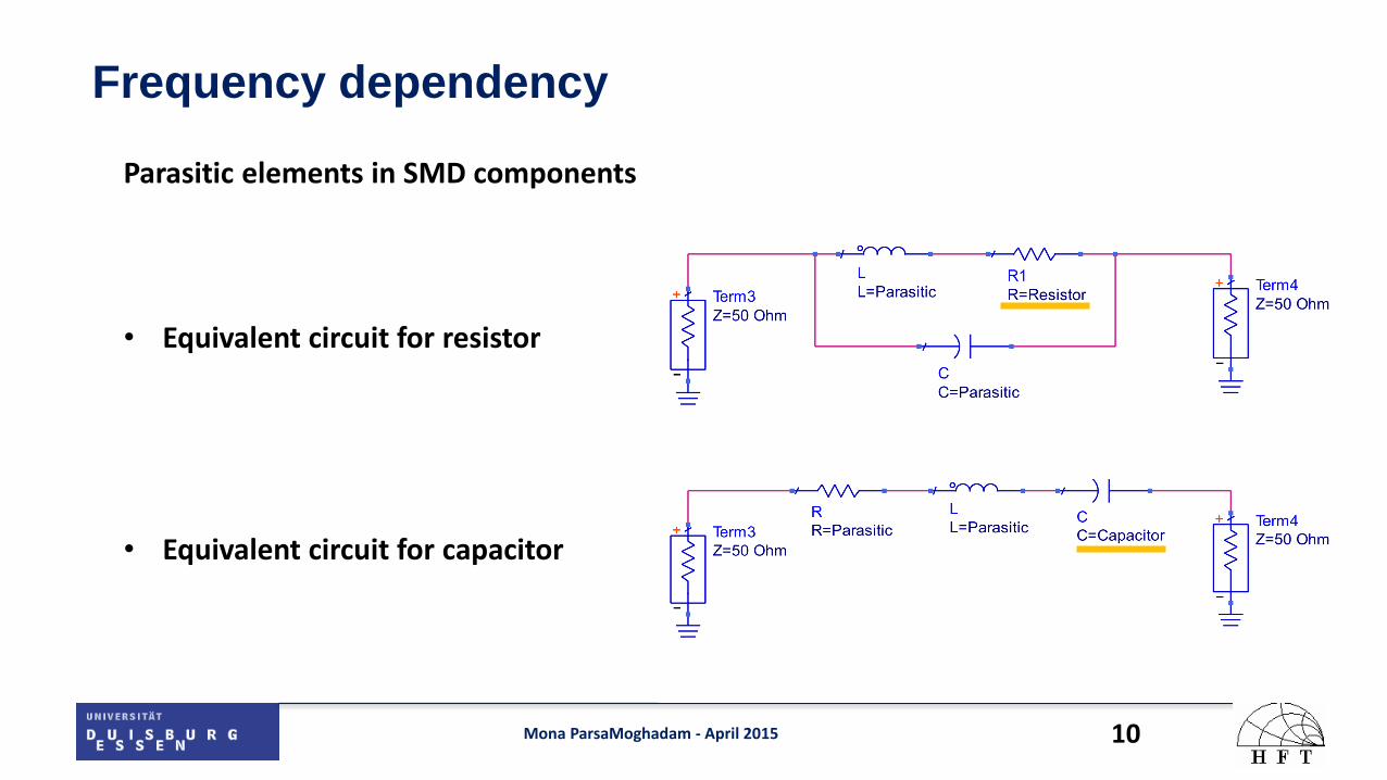
Frequency dependency
Mona ParsaMoghadam - April 2015 10
• Equivalent circuit for resistor
• Equivalent circuit for capacitor
Parasitic elements in SMD components
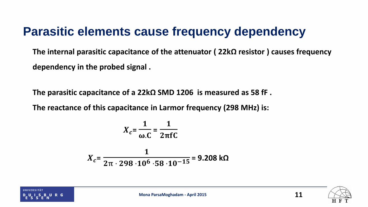
Parasitic elements cause frequency dependency
Mona ParsaMoghadam - April 2015 11
The internal parasitic capacitance of the attenuator ( 22kΩ resistor ) causes frequency
dependency in the probed signal .
𝑿𝒄= 𝟏
𝛚.𝐂 =
𝟏
𝟐𝛑𝐟𝐂
The parasitic capacitance of a 22kΩ SMD 1206 is measured as 58 fF .
The reactance of this capacitance in Larmor frequency (298 MHz) is:
𝑿𝒄= 𝟏
𝟐π · 𝟐𝟗𝟖 ·𝟏𝟎𝟔 ·𝟓𝟖 ·𝟏𝟎−𝟏𝟓 = 9.208 kΩ
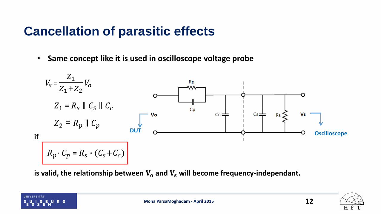
Cancellation of parasitic effects
Mona ParsaMoghadam - April 2015 12
• Same concept like it is used in oscilloscope voltage probe
𝑉𝑠 = 𝑍1
𝑍1+𝑍2 𝑉𝑜
𝑍1 = 𝑅𝑠 ‖ 𝐶𝑆 ‖ 𝐶𝑐
𝑍2 = 𝑅𝑝 ‖ 𝐶𝑝
𝑅𝑝· 𝐶𝑝 = 𝑅𝑠 · (𝐶𝑠+𝐶𝑐)
is valid, the relationship between 𝐕𝐨 and 𝐕𝐬 will become frequency-independant.
if DUT Oscilloscope
Mona ParsaMoghadam - April 2015 13
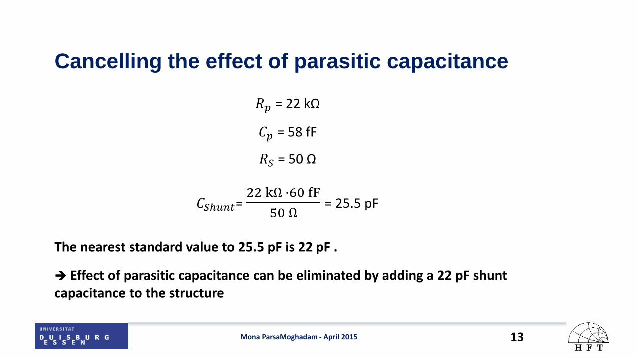
Cancelling the effect of parasitic capacitance
𝑅𝑝 = 22 kΩ
𝐶𝑝 = 58 fF
𝑅𝑆 = 50 Ω
𝐶𝑆ℎ𝑢𝑛𝑡= 22 kΩ ·60 fF
50 Ω = 25.5 pF
The nearest standard value to 25.5 pF is 22 pF .
Effect of parasitic capacitance can be eliminated by adding a 22 pF shunt capacitance to the structure
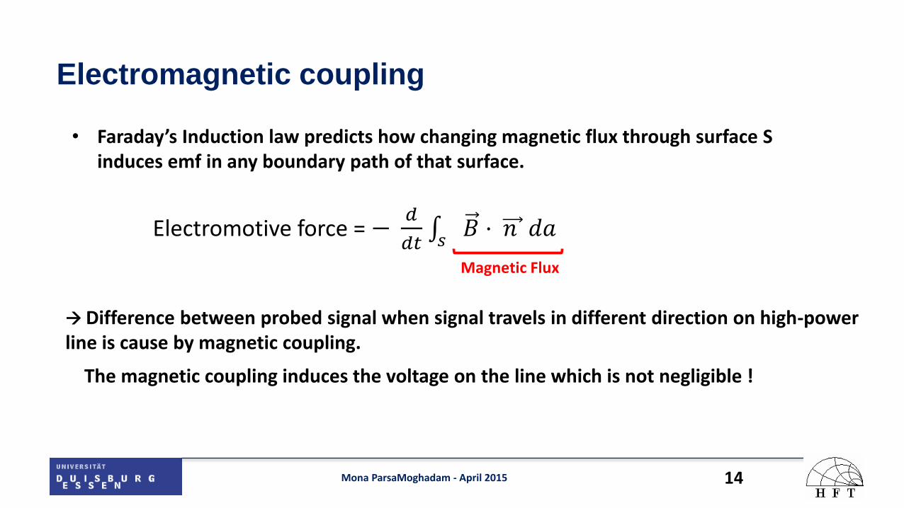
Electromagnetic coupling
Mona ParsaMoghadam - April 2015 14
Difference between probed signal when signal travels in different direction on high-power line is cause by magnetic coupling.
The magnetic coupling induces the voltage on the line which is not negligible !
• Faraday’s Induction law predicts how changing magnetic flux through surface S induces emf in any boundary path of that surface.
Electromotive force = − 𝑑
𝑑𝑡 𝐵𝑠
· 𝑛 𝑑𝑎
Magnetic Flux

Mona ParsaMoghadam - April 2015 15
There are various factors that affect the electromagnetic fields on the structure. Some of them are :
• Relative permittivity of substrate (ɛ𝒓)
• Substrate height
• Size of ground area between lines
Not so easy to predict electromagnetic field behavior in different part of the structure. The best way is to run electromagnetic simulation.
Outline
Mona ParsaMoghadam - April 2015 16
• Introduction
- Thesis work scope
- MRI system
- RF Power Amplifier / Cartesian Feedback Circuit
• Inaccuracy in Probing Voltage
- Parasitic Elements
- Electromagnetic coupling and induced voltage
• Electromagnetic Simulation
• Circuit Simulation
• Measurements
• Summary and Conclusion

Building up the Model in the Simulation Tool (Empire XPU)
Mona ParsaMoghadam - April 2015 17

Mona ParsaMoghadam - April 2015 18
Simulation results with and without shunt
capacitor
Probed signal without 𝐂𝐬𝐡𝐮𝐧𝐭
Probed signal with 𝐂𝐬𝐡𝐮𝐧𝐭
Mona ParsaMoghadam - April 2015 19
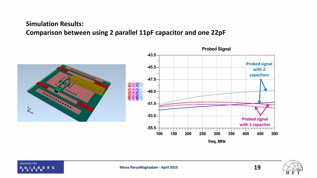
Simulation Results: Comparison between using 2 parallel 11pF capacitor and one 22pF
Probed signal with 2
capacitors
Probed signal with 1 capacitor
Mona ParsaMoghadam - April 2015 20
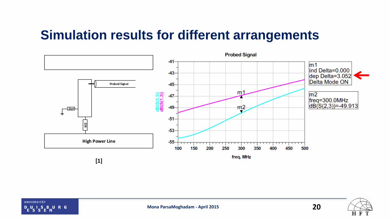
Simulation results for different arrangements
22K
22pF
High Power Line
Probed Signal
[1]
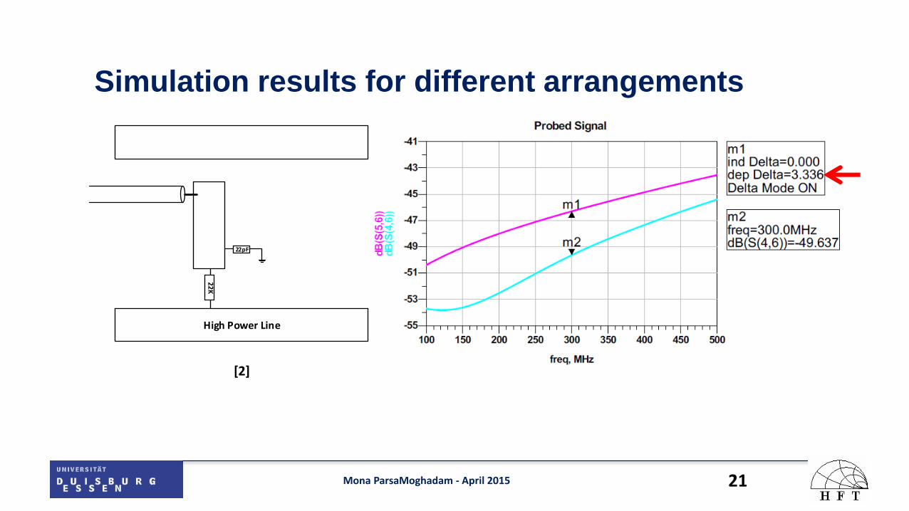
Mona ParsaMoghadam - April 2015 21
22K
22pF
High Power Line
[2]
Simulation results for different arrangements

Mona ParsaMoghadam - April 2015 22
22K
22pF
High Power Line
[3]
Probed Signal
Simulation results for different arrangements

Mona ParsaMoghadam - April 2015 23
22K
22pF
High Power Line
Probed Signal
[4]
Simulation results for different arrangements

Mona ParsaMoghadam - April 2015 24
5700µm
5300µm
4900µm
4500µm
4100µm
3700µm
3300µm
2900µm
2500µm
|S23-S13| dB 2,836 2,4844 2,0507 1,4548 1,0225 0,639 0,5018 0,2273 0,0063
0
0,5
1
1,5
2
2,5
3
Scat
teri
ng
Par
amet
ers
in d
B
|S23-S13| dB
Reducing induced voltage by shifting capacitor
near to coax cable
22K
22pF
High Power Line
Probed Signal
[4]
Mona ParsaMoghadam - April 2015 25
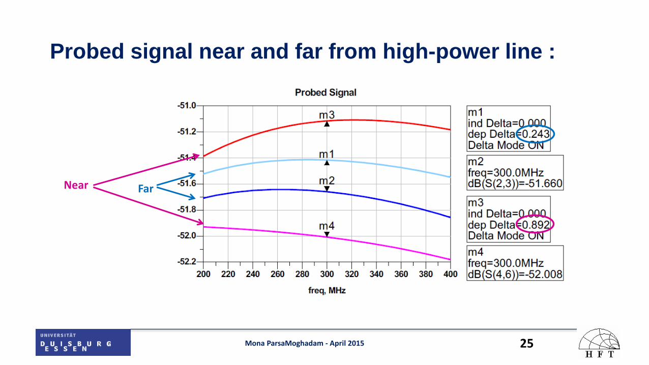
Probed signal near and far from high-power line :
Far
Near

Mona ParsaMoghadam - April 2015 26
Conclusion of EM Simulation
• The loop that is made by shunt capacitor and coax cable is the critical area. The magnetic flux pass through this area, induce emf on the line. • According to Faraday’s induction law the induced emf can be decreased by
- Minimizing the surface area that magnetic flux goes through - Getting far from high-power line for reducing magnetic filed strength

Outline
Mona ParsaMoghadam - April 2015 27
• Introduction
- Thesis work scope
- MRI system
- RF Power Amplifier / Cartesian Feedback Circuit
• Inaccuracy in Probing Voltage
- Parasitic Elements
- Electromagnetic coupling and induced voltage
• Electromagnetic Simulation
• Circuit Simulation
• Measurements
• Summary and Conclusion
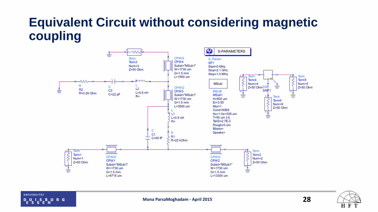
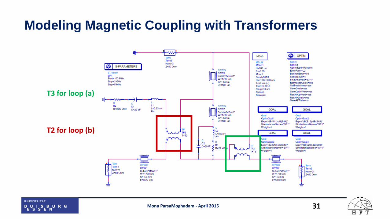
Equivalent Circuit without considering magnetic coupling
Mona ParsaMoghadam - April 2015 28
Mona ParsaMoghadam - April 2015 29
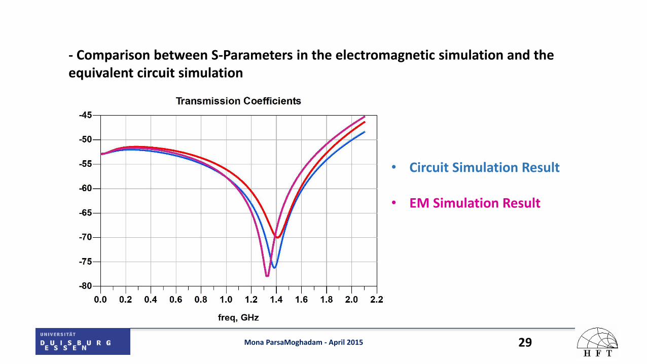
- Comparison between S-Parameters in the electromagnetic simulation and the equivalent circuit simulation
• Circuit Simulation Result • EM Simulation Result
Mona ParsaMoghadam - April 2015 30
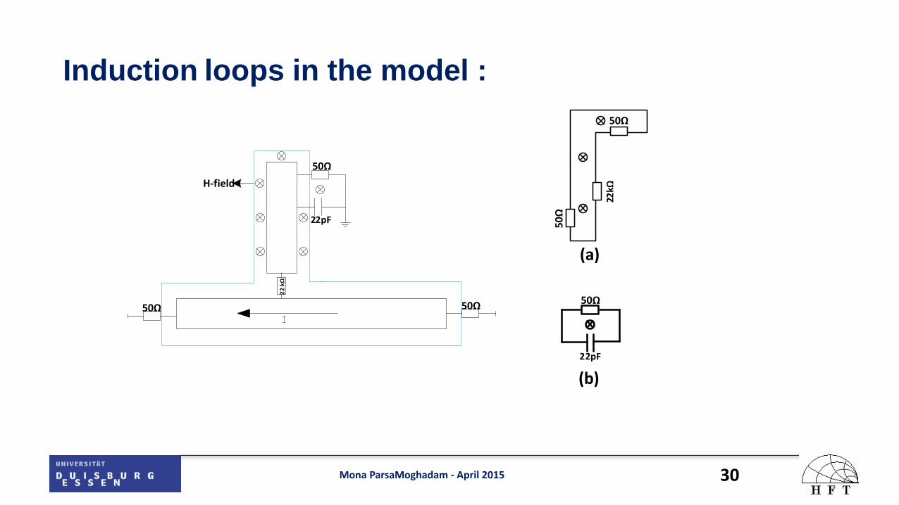
Induction loops in the model :
H-field
50Ω
50Ω
50Ω
22
kΩ
22pF
22kΩ
50Ω
50Ω
(a)
50Ω
22pF
(b)
Mona ParsaMoghadam - April 2015 31
Modeling Magnetic Coupling with Transformers
T3 for loop (a)
T2 for loop (b)
Mona ParsaMoghadam - April 2015 32
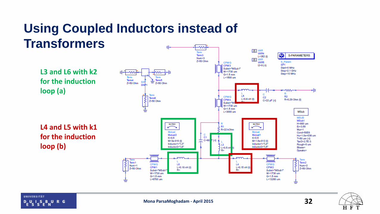
Using Coupled Inductors instead of
Transformers
L3 and L6 with k2 for the induction loop (a)
L4 and L5 with k1 for the induction loop (b)

Mona ParsaMoghadam - April 2015 33
The results after tuning the coupling factor match perfectly to the EM simulation results
Comparison between the Results
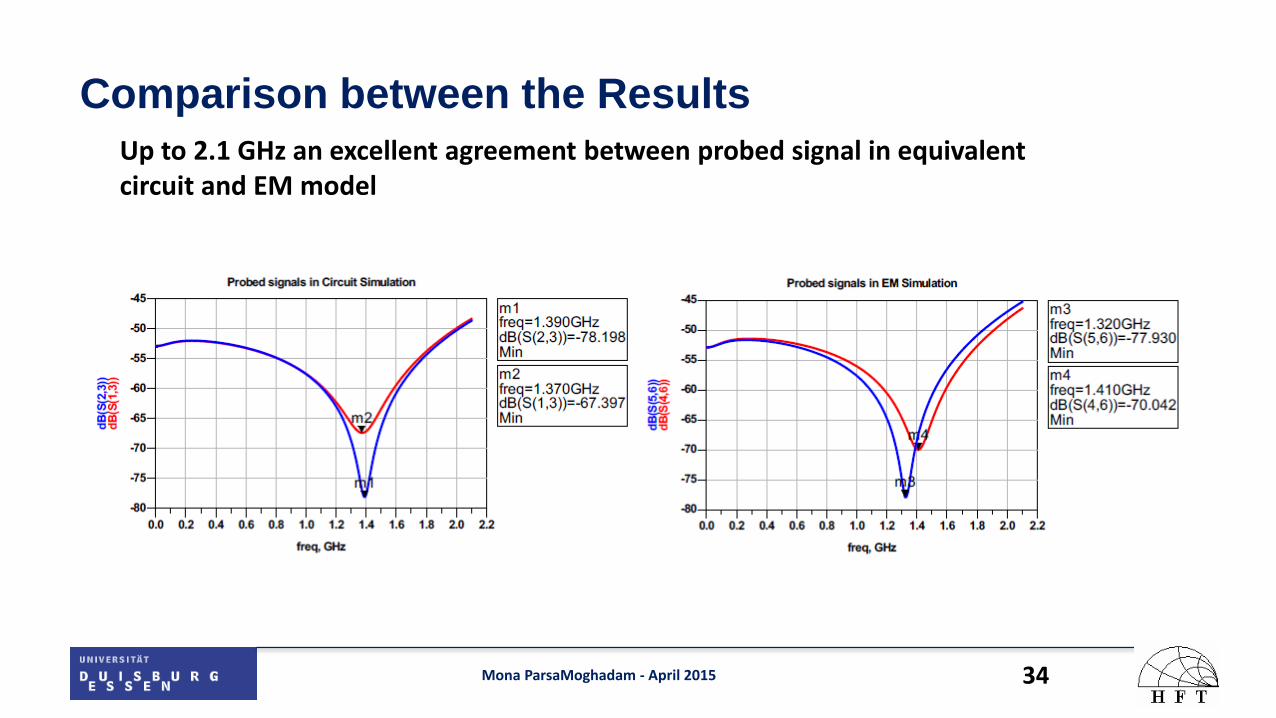
Mona ParsaMoghadam - April 2015 34
Up to 2.1 GHz an excellent agreement between probed signal in equivalent circuit and EM model
Comparison between the Results
Mona ParsaMoghadam - April 2015 35
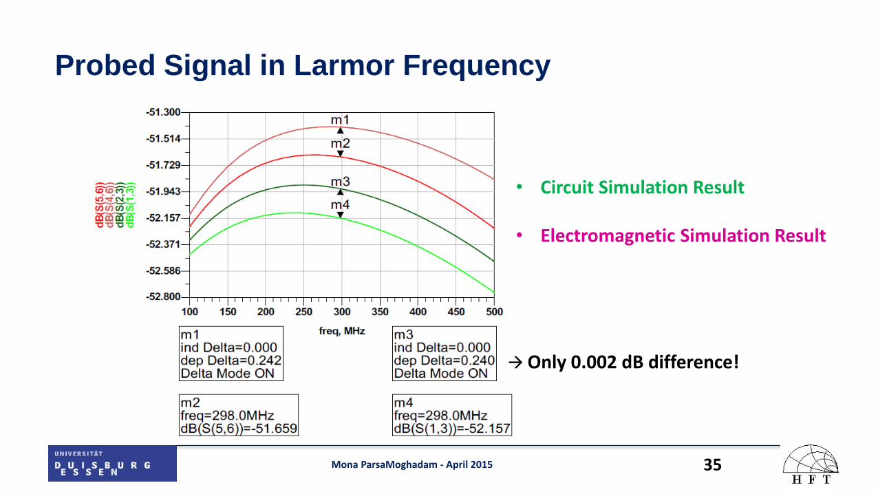
Probed Signal in Larmor Frequency
Only 0.002 dB difference!
• Circuit Simulation Result • Electromagnetic Simulation Result

Investigation of different coupling factors on the probed signal
Mona ParsaMoghadam - April 2015 36
Coupling Factor = k
0 ≤ k ≤ 1
No coupling Full coupling
For finding the dominant induction loop , k1 and k2 are shifted from minimum (k = 0) to maximum (k = 1) and the effects on the probed signal in the time domain is being observed.
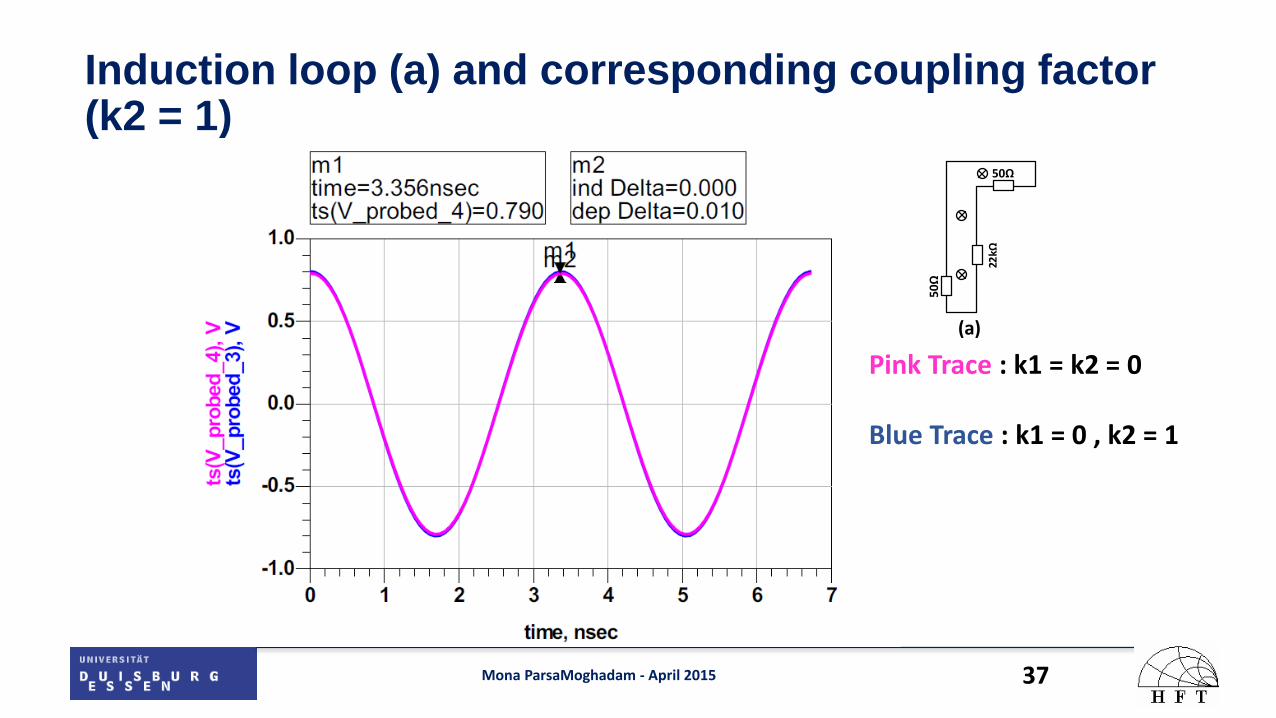
Induction loop (a) and corresponding coupling factor (k2 = 1)
Mona ParsaMoghadam - April 2015 37
Pink Trace : k1 = k2 = 0 Blue Trace : k1 = 0 , k2 = 1
22kΩ
50Ω
50Ω
(a)
Mona ParsaMoghadam - April 2015 38
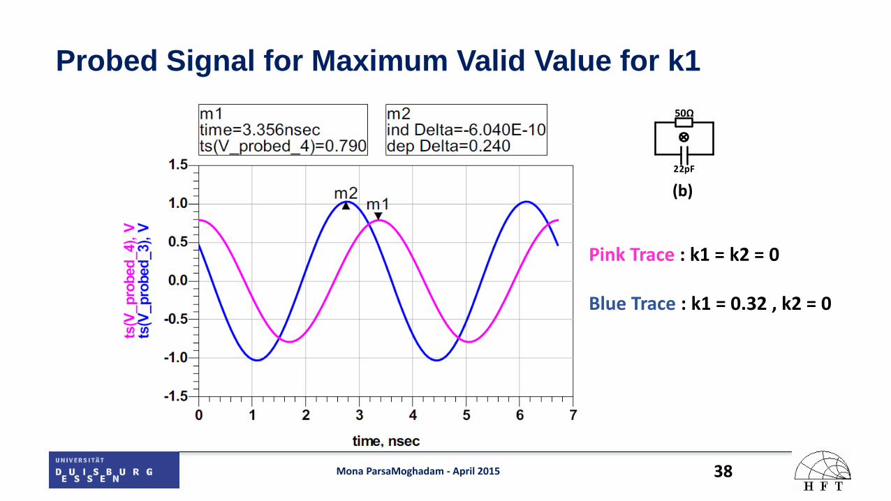
Probed Signal for Maximum Valid Value for k1
Pink Trace : k1 = k2 = 0 Blue Trace : k1 = 0.32 , k2 = 0
50Ω
22pF
(b)
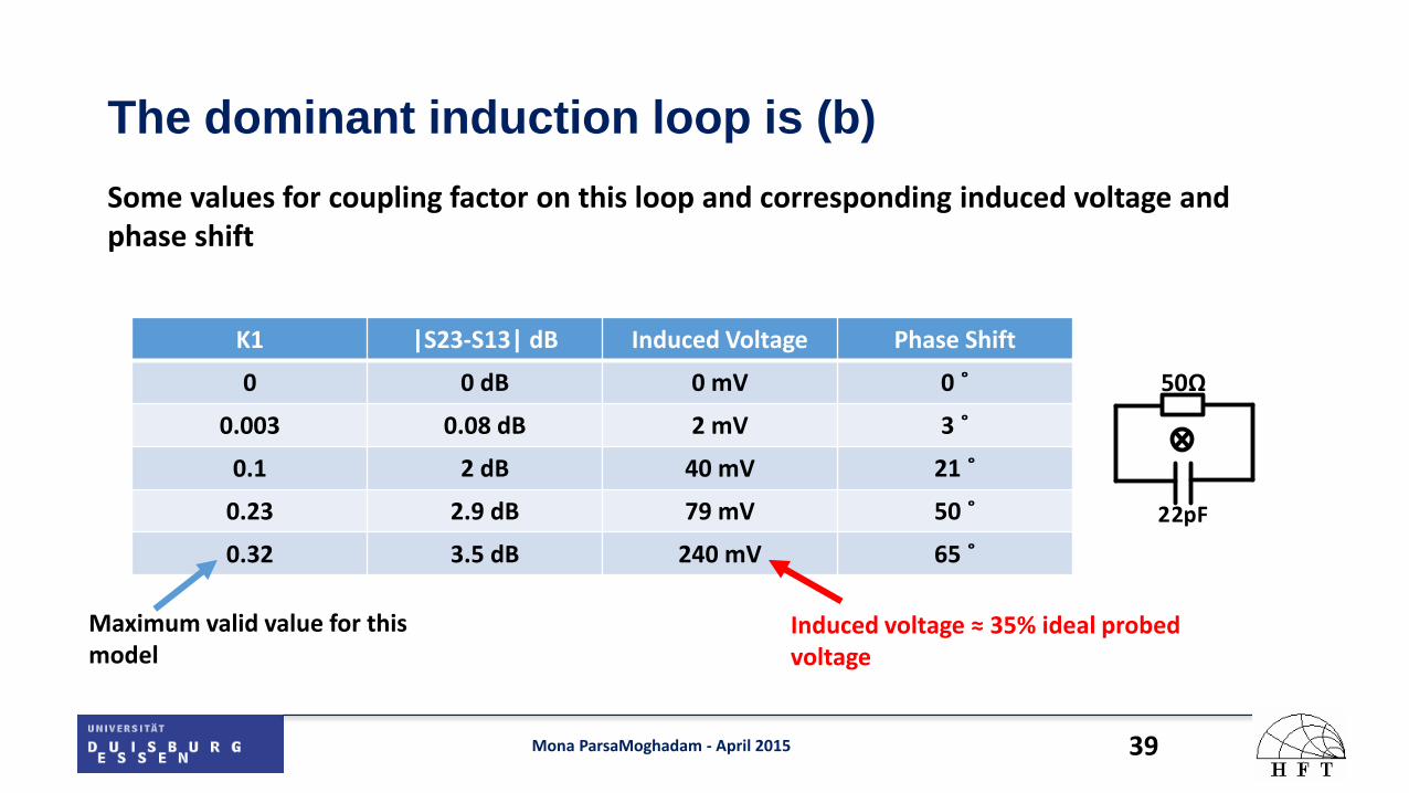
The dominant induction loop is (b)
Mona ParsaMoghadam - April 2015 39
Some values for coupling factor on this loop and corresponding induced voltage and phase shift
K1 |S23-S13| dB Induced Voltage Phase Shift
0 0 dB 0 mV 0 ˚
0.003 0.08 dB 2 mV 3 ˚
0.1 2 dB 40 mV 21 ˚
0.23 2.9 dB 79 mV 50 ˚
0.32 3.5 dB 240 mV 65 ˚
50Ω
22pF
(b)Maximum valid value for this model
Induced voltage ≈ 35% ideal probed voltage

Mona ParsaMoghadam - April 2015 40
Conclusion
Equivalent circuit simulation results also showed that the induction loop which is
created by shunt capacitor and coax cable is the critical area which can induce
voltage up to ≈250 mV.
Outline
Mona ParsaMoghadam - April 2015 41
• Introduction
- Thesis work scope
- MRI system
- RF Power Amplifier / Cartesian Feedback Circuit
• Inaccuracy in Probing Voltage
- Parasitic Elements
- Electromagnetic coupling and induced voltage
• Electromagnetic Simulation
• Circuit Simulation
• Measurements
• Summary and Conclusion

PCB Model for Measurements
Mona ParsaMoghadam - April 2015 42
- Measurements are done on a
PCB which reflects the output
part of the RF power amplifier
where the voltage is probed
- PCB size = 2cm × 3cm !

Measurement results for showing the effect of shunt capacitor
Mona ParsaMoghadam - April 2015 43
Red Trace : with 𝐂𝐬𝐡𝐮𝐧𝐭 Blue Trace : without 𝐂𝐬𝐡𝐮𝐧𝐭
Measurement Results for Extreme Cases
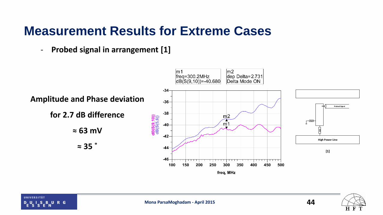
Mona ParsaMoghadam - April 2015 44
- Probed signal in arrangement [1]
Amplitude and Phase deviation
for 2.7 dB difference
≈ 63 mV
≈ 35 ˚
22K
22pF
High Power Line
Probed Signal
[1]

Measurement Results for Extreme Cases
Mona ParsaMoghadam - April 2015 45
- Shunt capacitor far from the coax cable
Amplitude and Phase deviation
for 1.96 dB difference
≈ 35 mV
≈ 19 ˚

Measurement Results for Extreme Cases
Mona ParsaMoghadam - April 2015 46
- Shunt capacitor in the middle of junction and coax cable
Amplitude and Phase deviation
for 1.19 dB difference
≈ 20 mV
≈ 10 ˚

Measurement Results for Extreme Cases
Mona ParsaMoghadam - April 2015 47
- Shunt capacitor near to the coax cable
Amplitude and Phase deviation
for 0.3 dB difference
≈ 10 mV
≈ 4 ˚
Outline
Mona ParsaMoghadam - April 2015 48
• Introduction
- Thesis work scope
- MRI system
- RF Power Amplifier / Cartesian Feedback Circuit
• Inaccuracy in Probing Voltage
- Parasitic Elements
- Electromagnetic coupling and induced voltage
• Electromagnetic Simulation
• Circuit Simulation
• Measurements
• Summary and Conclusion

Summary
Mona ParsaMoghadam - April 2015 49
• In an MRI smart power amplifier, the accuracy of the probed voltage is very important.
• Magnetic coupling can induce a voltage up to ≈ 250 mV. EM simulations were done to find the best arrangement of elements for minimizing the induced voltage
• The critical induction loop which caused the most induced voltage is the loop which is created by the coax cable + a part of the transmission line + shunt capacitor
• An equivalent circuit was given for modeling the voltage probe + magnetic coupling
• Measurements were done to support the simulation results.
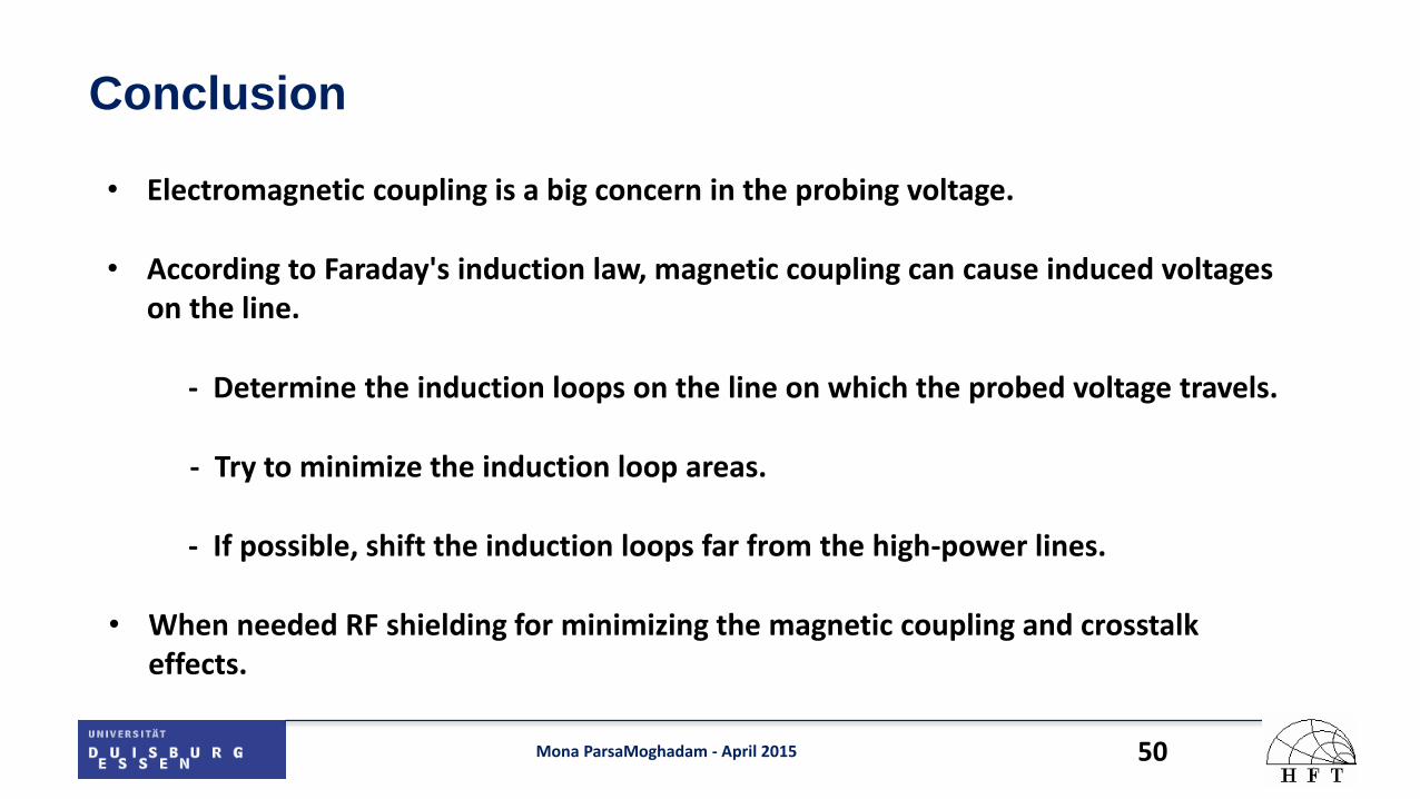
Conclusion
Mona ParsaMoghadam - April 2015 50
• Electromagnetic coupling is a big concern in the probing voltage.
• According to Faraday's induction law, magnetic coupling can cause induced voltages on the line.
- Determine the induction loops on the line on which the probed voltage travels.
- Try to minimize the induction loop areas.
- If possible, shift the induction loops far from the high-power lines.
• When needed RF shielding for minimizing the magnetic coupling and crosstalk effects.

Mona ParsaMoghadam - April 2015 51
Thank you for your attention!
Mona ParsaMoghadam - April 2015 52
Backup slides
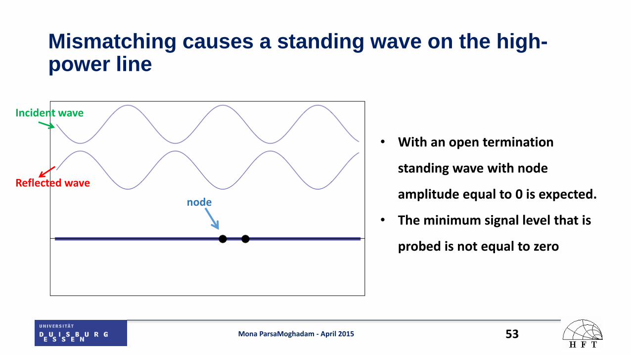
Mismatching causes a standing wave on the high-power line
Mona ParsaMoghadam - April 2015 53
• With an open termination
standing wave with node
amplitude equal to 0 is expected.
• The minimum signal level that is
probed is not equal to zero
node
Incident wave
Reflected wave


![A collection of computer programs for two-probe …...Intheareaofelectricalprofiling,two-probespreadingresistance[4]andcapacitance-voltage [5] are probably the most widely used techniques.Capacitance-voltage](https://static.fdocuments.in/doc/165x107/5e4df5ca0727fc16fc3c44e9/a-collection-of-computer-programs-for-two-probe-intheareaofelectricalprofilingtwo-probespreadingresistance4andcapacitance-voltage.jpg)
